US9150411B2 - Fusing method of substrate layer, manufacturing method of microfluidic chip and fusing apparatus of substrate layer - Google Patents
Fusing method of substrate layer, manufacturing method of microfluidic chip and fusing apparatus of substrate layer Download PDFInfo
- Publication number
- US9150411B2 US9150411B2 US13/663,211 US201213663211A US9150411B2 US 9150411 B2 US9150411 B2 US 9150411B2 US 201213663211 A US201213663211 A US 201213663211A US 9150411 B2 US9150411 B2 US 9150411B2
- Authority
- US
- United States
- Prior art keywords
- substrate layer
- organic solvent
- resin
- temperature
- substrate
- Prior art date
- Legal status (The legal status is an assumption and is not a legal conclusion. Google has not performed a legal analysis and makes no representation as to the accuracy of the status listed.)
- Active, expires
Links
Images


Classifications
-
- B—PERFORMING OPERATIONS; TRANSPORTING
- B81—MICROSTRUCTURAL TECHNOLOGY
- B81C—PROCESSES OR APPARATUS SPECIALLY ADAPTED FOR THE MANUFACTURE OR TREATMENT OF MICROSTRUCTURAL DEVICES OR SYSTEMS
- B81C3/00—Assembling of devices or systems from individually processed components
- B81C3/001—Bonding of two components
-
- B—PERFORMING OPERATIONS; TRANSPORTING
- B29—WORKING OF PLASTICS; WORKING OF SUBSTANCES IN A PLASTIC STATE IN GENERAL
- B29C—SHAPING OR JOINING OF PLASTICS; SHAPING OF MATERIAL IN A PLASTIC STATE, NOT OTHERWISE PROVIDED FOR; AFTER-TREATMENT OF THE SHAPED PRODUCTS, e.g. REPAIRING
- B29C65/00—Joining or sealing of preformed parts, e.g. welding of plastics materials; Apparatus therefor
- B29C65/48—Joining or sealing of preformed parts, e.g. welding of plastics materials; Apparatus therefor using adhesives, i.e. using supplementary joining material; solvent bonding
- B29C65/4895—Solvent bonding, i.e. the surfaces of the parts to be joined being treated with solvents, swelling or softening agents, without adhesives
-
- B—PERFORMING OPERATIONS; TRANSPORTING
- B81—MICROSTRUCTURAL TECHNOLOGY
- B81B—MICROSTRUCTURAL DEVICES OR SYSTEMS, e.g. MICROMECHANICAL DEVICES
- B81B2201/00—Specific applications of microelectromechanical systems
- B81B2201/05—Microfluidics
- B81B2201/058—Microfluidics not provided for in B81B2201/051 - B81B2201/054
-
- B—PERFORMING OPERATIONS; TRANSPORTING
- B81—MICROSTRUCTURAL TECHNOLOGY
- B81C—PROCESSES OR APPARATUS SPECIALLY ADAPTED FOR THE MANUFACTURE OR TREATMENT OF MICROSTRUCTURAL DEVICES OR SYSTEMS
- B81C2201/00—Manufacture or treatment of microstructural devices or systems
- B81C2201/01—Manufacture or treatment of microstructural devices or systems in or on a substrate
- B81C2201/0174—Manufacture or treatment of microstructural devices or systems in or on a substrate for making multi-layered devices, film deposition or growing
- B81C2201/019—Bonding or gluing multiple substrate layers
-
- B—PERFORMING OPERATIONS; TRANSPORTING
- B81—MICROSTRUCTURAL TECHNOLOGY
- B81C—PROCESSES OR APPARATUS SPECIALLY ADAPTED FOR THE MANUFACTURE OR TREATMENT OF MICROSTRUCTURAL DEVICES OR SYSTEMS
- B81C2203/00—Forming microstructural systems
- B81C2203/03—Bonding two components
- B81C2203/033—Thermal bonding
- B81C2203/037—Thermal bonding techniques not provided for in B81C2203/035 - B81C2203/036
Definitions
- the present application relates to a fusing method of a substrate layer, a manufacturing method of a microfluidic chip and a fusing apparatus of a substrate layer, and particularly to a fusing method of a substrate layer capable of performing superimposition of substrate layers by preventing deformation of a region formed on the substrate layer.
- a microchip electrophoresis method of performing capillary electrophoresis using a microfluidic chip on which capillaries are formed by preparing a flow path (fine groove) on a plastic substrate layer and superimposing the substrate layer on an additional sheet of the substrate layer has been disclosed (refer to Japanese Unexamined Patent Application Publication No. 2004-219199 and Japanese Unexamined Patent Application Publication No. 2001-242138).
- the microchip electrophoresis method is used in analyses of chargeable trace substance such as nucleic acids, proteins, viruses, cells, amino acids, sugars, organic acids and ions.
- microfluidic chip on which a sample introduction flow path and a sample separation flow path are formed so as to be at right angles to each other has been used (refer to FIG. 3 of Japanese Unexamined Patent Application Publication No. 2004-219199).
- an electrode is formed in the vicinity of an end point of the sample separation flow path using a printing method, a vapor deposition method, an etching method, a plating method or the like, and conductive path wiring for electrophoresis is performed (refer to Japanese Unexamined Patent Application Publication No. 2001-242138).
- a microfluidic chip having regions such as wells or fluid paths is manufactured by superimposing substrate layers having the regions formed.
- the superimposition may be performed by heating and crimping the heated substrate layer up to the glass transition temperature or the softening point temperature of a resin.
- the regions formed on the substrate layer are deformed due to pressure during crimping.
- the softening of the resin may be insufficient and joining may be not be completed.
- the joining has a tendency not to be complete in the vicinity of the electrode which is convex at the joining surface and a gap may be formed at a joining interface.
- the present disclosure provides a fusing method of a substrate layer including the following (1) and (2).
- a temperature during the crimping may be suppressed to less than a glass transition temperature or a softening point temperature of a resin (hereinafter, both temperatures are referred to as “the glass transition temperature”).
- the fusing method may also include the following (3) and (4). Removing and pressurizing may lead to more complete joining of the substrate layer crimped during the heating and crimping.
- the fusing method is preferably adaptable to a case where a region which becomes a reaction field or an analysis field of a substance is formed on the substrate layer, and is more preferably adaptable to a case where the substrate layer has a minute level difference on the joining surface.
- As the level difference what is present between an electrode formed at the joining surface and the surface may be exemplified.
- the joining surface may be preferably treated using a vaporized form of the organic solvent.
- the opposite side surface to the joining surface of the substrate layer may be preferably pressed via a buffer material.
- the present disclosure provides a manufacturing method of a microfluidic chip including the following (1A) and (2A). According to the manufacturing method, a microfluidic chip in which the regions are not deformed may be obtained.
- the present disclosure provides a manufacturing method of a microfluidic chip including the following (1B) to (4B). According to the manufacturing method, a microfluidic chip where a level difference of the joining surface is sealed with the resin may be obtained.
- the present disclosure also provides a fusing apparatus of a substrate layer including a dissolving unit that treats a joining surface of the substrate formed from a resin using an organic solvent having solubility with respect to the resin, a crimping unit that heats the substrate layer treated using the organic solvent at a temperature less than the glass transition temperature of the resin and crimping the heated substrate layer, and a pressurizing unit that pressurizes the crimped substrate layer after removing the organic solvent while heating at a temperature higher than a heating temperature during the crimping and lower than the glass transition temperature of the resin in the crimping unit.
- the present application provides a fusing method of a substrate layer capable of performing superimposition of substrate layers through preventing a deformation of a region formed.
- FIG. 1 is a flow chart illustrating procedures of a fusing method of a substrate layer according to the present application
- FIGS. 2A and 2B are schematic diagrams illustrating a configuration of a microfluidic chip A to be preferably manufactured using a fusing method of a substrate layer according to the present application;
- FIG. 3 is a schematic diagram illustrating a configuration of a substrate layer of a microfluidic chip
- FIG. 4 is a schematic diagram illustrating a configuration of another substrate layer of the microfluidic chip
- FIGS. 5A and 5B are schematic diagrams illustrating a state ( FIG. 5A ) in which a gap is present at a joining interface of the substrate layers and a state FIG. 5B where the gap is not present;
- FIG. 6 is a block diagram illustrating a configuration of a fusing apparatus of a substrate layer according to the present application
- FIG. 7 is a graph as a substitute for a drawing illustrating an example of a change in a pressurizing force and a change in a molding die temperature of a hot pressing unit used in an embodiment
- FIGS. 8A and 8B are pictures as a substitute for a drawing where peripheral portions of an electrode prior to pressurizing ( FIG. 8A ) and after pressurizing ( FIG. 8B ) of a microfluidic chip manufactured in an embodiment are photographed.
- FIG. 1 is a flow chart illustrating a fusing method of a substrate layer according to the present application.
- FIGS. 2A to 4 are schematic diagrams illustrating an example of a microfluidic chip to be preferably manufactured using a fusing method of a substrate layer according to the present application.
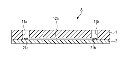
- FIG. 2A , FIG. 3 and FIG. 4 are top view schematic diagrams
- FIG. 2B is a cross sectional schematic diagram corresponding to IIB-IIB cross section in FIG. 2A .
- the microfluidic chip represented by reference numeral A is used in a microchip electrophoresis method and formed by superimposing a substrate layer 1 and a substrate layer 2 .
- the substrate layer 1 has four feed openings 11 a , 11 b , 11 c and 11 d penetrated in order to feed a sample.
- groove shaped flow paths 12 a (sample separation flow path) and 12 b (sample introduction flow path) communicating with the feed openings are formed so as to be at right angles to each other.
- the substrate layer 2 has electrodes 21 a , 21 b , 21 c and 21 d at positions corresponding to the feed openings 11 a , 11 b , 11 c and 11 d of the substrate layer 1 .
- the electrodes 21 a , 21 b , 21 c and 21 d become conducting paths for the electrophoresis of the sample inside the flow paths 12 a and 12 b.
- the microfluidic chip A is manufactured by superimposing a surface on which the electrodes of the substrate layer 2 are formed and a surface on which the flow paths of the substrate layer 1 are arranged in such a manner that the electrodes 21 a , 21 b , 21 c and 21 d arranged on the substrate 2 may be respectively located inside the feed openings 11 a , 11 b , 11 c and 11 d arranged on the substrate layer 1 .
- the materials of the substrate layers 1 and 2 may be a plastic used as a material in the related art, such as polypropylene, polycarbonate, polymethyl methacrylate, cycloolefin polymer or polydimethylsiloxane.
- a plastic used as a material in the related art such as polypropylene, polycarbonate, polymethyl methacrylate, cycloolefin polymer or polydimethylsiloxane.
- the material of the substrate layers 1 and 2 it is preferable to select a material with less optical error in order to have an optical transparency, less auto-fluorescence and less wavelength dispersion.
- polycarbonate which also has an excellent heat resistance property in addition to the optical property is more preferable.
- the materials of the substrate layers 1 and 2 may be either identical or different.
- the substrate layer 1 may be a substrate which is approximately 25 mm in height, 75 mm in width and 1 mm in thickness.
- the substrate layer 2 may be a sheet or film which is approximately 25 mm in height, 75 mm in width and 50 to 200 ⁇ m in thickness.
- the feed openings 11 a , 11 b , 11 c and 11 d and the flow paths 12 a and 12 b may be molded on the substrate layer 1 using nanoimprint lithography, injection molding, cutting work or the like.
- a pillar which is approximately 10 to 500 ⁇ m in width and 10 to 300 ⁇ m in height may be formed in order to function as a filter when necessary.
- the size of the flow paths 12 a and 12 b is especially but not limited, for example, the width may be approximately 10 to 500 ⁇ m and the depth may be approximately 10 to 300 ⁇ m.
- the material of the electrodes 21 a , 21 b , 21 c and 21 d especially but not limited to an electrically conducting material such as carbon, gold and silver, carbon is preferably used.
- the electrode material may not adsorb and deactivate the material introduced into the flow paths 12 a and 12 b , and the reaction product thereof.
- a printing method, a vapor deposition method, an etching method or a plating method in the related art may be performed.
- the thickness may be approximately 2 to 10 ⁇ m.
- obtaining a microfluidic chip A by superimposing substrate layers 1 and 2 is described in order.
- the dissolving S 1 treats a joining surface of the substrate layers 1 and 2 using an organic solvent having solubility with respect to a resin forming the substrate layers 1 and 2 .
- the joining surface of the substrate layer 1 is a surface on which flow paths 12 a and 12 b are formed and the joining surface of the substrate layer 2 is a surface on which electrodes 21 a , 21 b , 21 c and 21 d are formed.
- the joining surface is softened.
- a crimping temperature of the substrate layer in the below described crimping S 2 may be suppressed to less than a glass transition temperature (melting point) of a resin.
- the “glass transition temperature (melting point)” may be replaced with a “softening point temperature (melting point)”.
- the organic solvent As the organic solvent, according to a material of the substrate layers 1 and 2 , a solvent having solubility for the material is appropriately used.
- the organic solvent used may be tetrahydrofuran, ethyl acetate, chloroform, aceton, methyl chloride, 2-propanol, ethanol, cyclohexane, toluene, xylene, octane or the like.
- chloroform is preferably used as the organic solvent.
- the organic solvent may not adsorb and deactivate the material introduced into the flow paths 12 a and 12 b , and the reaction product thereof.
- the treatment using the organic solvent is performed on at least one side of the joining surface of the substrate layer 1 and the joining surface of the substrate layer 2 .
- the treatment of the organic solvent is preferably performed at the joining surface of the substrate layer 1 only.
- the surface opposite the joining surface of the substrate layer may be preferably protected by film or the like such that it is not in contact with the organic solvent.
- the treatment using the organic solvent may be performed by bringing a liquid organic solvent into contact with the joining surface, but may be preferably performed by bringing a vaporized organic solvent into contact with the joining surface.
- the treatment using the organic solvent may be performed by merely lowering the softening temperature of the resin at the joining interface of the substrate layers 1 and 2 .
- the organic solvent permeates through up to a deep position from the surface layer of the joining surface of the substrate layers 1 and 2 and softens the resin. Accordingly, a shape change may be caused in the flow paths 12 a and 12 b formed on the substrate layer 1 and the solvent crack may occur.
- the treatment time using one organic solvent may be appropriately set according to the material of the substrate layer and the organic solvent used. However, if the treatment time is too short, an effect of lowering the crimping temperature in the crimping S 2 may not be obtained. If too long, a deformation of the flow paths 12 a and 12 b may occur in the crimping S 2 .
- the substrate layers 1 and 2 after the organic solvent treatment are superimposed so that the joining surfaces of the substrate layers 1 and 2 are faced each other, placed on a hot pressing unit, pressurized and crimped while being heated using a heater.
- the joining surface is treated using the organic solvent and softened in the dissolving S 1 , in this procedure, the substrate layer may be sufficiently joined by thermal compression at less than a glass transition temperature of the resin.
- the shape change in the flow paths 12 a and 12 b , or the like which was a problem in the related art, may be prevented in thermal compression close to the glass transition temperature.
- twisting and warping do not occur on the substrate layers 1 and 2 after joining and the occurrence of auto-fluorescence of the substrate layers due to thermal cracking of the resin may be also suppressed.
- the heating temperature, pressurizing force and pressurizing time may be appropriately set according to the material of the substrate layer and the organic solvent used in the dissolving S 1 . However, if the temperature, pressure and time are excessively small, the joining of the substrate layer may be insufficient. If excessively large, deformation occurs in the flow paths 12 a and 12 b.
- the surface of the opposite side to the joining surface of the substrate layers 1 and 2 is pressed via a buffer material.
- a buffer material a member having heat resistance and elasticity such as a heat-resistant fluorine rubber may be used.
- FIG. 5A schematically illustrates a gap (refer to reference numeral V) that is formed in the vicinity of the electrode.
- the gap V appears at the joining interface, the sample introduced into the flow paths 12 a and 12 b leaks out from the gap V or without holding electrical insulation properties, the electrophoresis of the sample inside the flow paths 12 a and 12 b may not be possible.
- Such a gap may appear at the periphery of the joining surface even in a case where a minute level difference appears thereon due to the occurrence of a molding failure, a so-called “burr” or “undercutting” during the molding of the substrate layer. It is understood that a burr is likely to appear at the portion in contact with the molding die of thermoplastic resins during the injection molding of the substrate layer. Even a burr having a convex portion of approximately 2 to 10 ⁇ m in height may cause a gap V to appear.
- Using the buffer material may prevent the pressure from being concentrated on the convex portion such as the electrode and the burr during the pressing, eliminate non-uniformity on the side pressurized due to the variation of the thickness of the substrate layers 1 and 2 and thereby the gap V is not likely to appear.
- the joining of the substrate layers 1 and 2 may be preferably further completed.
- the organic solvent remaining on the crimped substrate layers 1 and 2 is completely removed.
- Removing the organic solvent may be performed by natural drying, air-drying or the like. However, removing by placing the crimped substrate layers 1 and 2 inside an oven heated at a higher temperature (approximately 60° C.) than room temperature is preferable.
- the softening temperature of the substrate layer lowered by the organic solvent may return to the original softening temperature of the resin.
- the removing is also necessary for preventing the organic solvent remained inside the microfluidic chip A from causing a solvent crack or whitening.
- the crimped substrate layers 1 and 2 are pressurized while being heated at a temperature which is higher than the heating temperature in the crimping S 2 and lower than the glass transition temperature of the resin.
- pressurization is performed at a higher temperature than the heating temperature in the crimping S 2 . Therefore, the substrate layer may even be joined at the positions of the gap V remaining at the joining interface of the substrate layers 1 and 2 after the crimping S 2 .
- the pressurizing may be performed such that the level difference occurred by the electrode or the burr in the adhering position is completely sealed by the resin (refer to FIG. 5B ).
- the heating temperature, pressurizing force and pressurizing time may be appropriately set according to the material of the substrate layer. However, if the temperature, pressure and time are excessively insufficient, no effect is expected in eliminating the gap. If excessively enough, deformation occurs in the flow paths 12 a and 12 b.
- the organic solvent remained on the substrate layers 1 and 2 is removed and the softening temperature of the substrate layer returns to the original softening temperature of the resin. Accordingly, in the pressurizing, even if the pressurizing is performed at a higher temperature than that of the crimping S 2 , a shape change does not occur in the flow paths 12 a and 12 b.
- the buffer material Even in the pressurizing, via the buffer material, the surface of the opposite side to the joining surface of the substrate layers 1 and 2 is pressed. Using the buffer material may prevent the pressure from being concentrated on the convex portion such that the gap V does not appear.
- thermal compression of the substrate layer may be possible at less than the glass transition temperature of the resin and thereby a microfluidic chip where the shape is not changed in the flow path or the like may be obtained.
- the resin is fitted to the level difference in the pressurizing S 4 and a microfluidic chip where the gap is not present on the level difference portion may be obtained.
- FIG. 6 is a block diagram illustrating a configuration of a fusing apparatus of a substrate layer according to the present application.
- the fusing apparatus represented by reference numeral 3 includes a feed unit 31 , a dissolving unit 32 , a fusing unit 33 , a discharging unit 34 and a mechanism for transporting the substrate layer therebetween.
- the fusing unit 33 is formed of a crimping unit 331 and a pressurizing unit 332 .
- the feed unit 31 holds a plurality of substrate layers on which a region such as the flow path and/or the substrate layers to be superimposed thereto.
- the feed unit 31 sends the held substrate layers to the dissolving unit 32 .
- the dissolving unit 32 includes a surface treatment device which treats the joining surface of the substrate layer fed from the feed unit 31 using an organic solvent having solubility with respect to the resin forming the substrate layer.
- the surface treatment device may be an exposure treatment device using the organic solvent in addition to an immersion device, a spray device or the like. It is preferable that the spray device brings the vaporized organic solvent into contact only with the joining surface of the substrate layer.
- the substrate layer after treatment is sent to the fusing unit 33 .
- the crimping unit 331 of the fusing unit 33 includes a hot pressing device which crimps the substrate layer conveyed from the dissolving unit 32 through heating at less than the glass transition temperature of the resin.
- the pressurizing unit 332 of the fusing unit 33 includes the hot pressing device which pressurizes the substrate layer crimped in the crimping unit 331 while heating at a temperature which is higher than the heating temperature in the crimping unit 331 and lower than the glass transition temperature of the resin.
- the hot pressing device configuring the crimping unit 331 and the pressurizing unit 332 includes a pressurizing mechanism such as a crimping head which superimposes and pressurizes the joining surfaces of the substrate layers so that the joining surfaces of the substrate layers 1 and 2 are opposed each other, and a heating mechanism such as a heater which heats the pressurizing mechanism.
- the substrate layer joined in the fusing unit 33 becomes a microfluidic chip and is sent to the discharging unit 34 .
- the hot pressing devices configuring the crimping unit 331 and the pressurizing unit 332 may be either identical or different.
- a conveying mechanism is provided between the respective devices and a drying mechanism is provided on a conveying route from the hot pressing device of the crimping unit 331 to the hot pressing device of the pressurizing unit 332 in order to remove the organic solvent remained on the substrate layer after crimping in the crimping unit 331 .
- the drying mechanism may be a wind blower, an oven or the like.
- the drying mechanism is provided in the hot pressing device in order to remove the organic solvent remained on the substrate layer during the crimping and the pressurizing.
- the fusing method of the substrate layer according to the present application may be also configured as follows.
- a fusing method of a substrate layer including: dissolving that treats a joining surface of a substrate layer formed from a resin using an organic solvent having solubility with respect to the resin; and crimping that crimps the treated substrate layer through heating at less than a glass transition temperature.
- the microfluidic chip illustrated In FIGS. 2A to 4 is manufactured for trial.
- a substrate layer 1 is molded using injection molding.
- a disk is manufactured in a manner that on, a passage for the flow path is carved out of a nickel plated stainless steel sheet having a sufficient thickness with respect to a depth of flow paths 12 a and 12 b using an end mill and a periphery of the passage is engraved.
- the manufactured disk is mounted on an injection molding machine and the substrate layer 1 is molded from polycarbonate resin.
- a substrate 2 is manufactured by silk screen printing of the electrodes 21 a , 21 b , 21 c and 21 d on the polycarbonate sheet.
- a conductive ink a carbon (Electrodag 423SS, Henkel Japan Ltd.) is used.
- the electrode for capillary electrophoresis it is preferable to have a surface resistivity of less than 5000 ⁇ /sq in order to suppress Joule heat generation. For this reason, a relationship between a printing thickness of the conductive ink (thickness of the electrode) and the surface resistivity is examined.
- the average surface resistivity is 1.39 k ⁇ /sq when the electrode thickness is 4 ⁇ m, is average 2.52 k ⁇ /sq in the electrode thickness 3.5 ⁇ m and is average 4.88 k ⁇ /sq in the electrode thickness 3 ⁇ m.
- the electrode thickness is set to be 3.5 ⁇ m.
- Vaporized ethanol, ethyl acetate, tetrahydrofuran and chloroform are applied to a joining surface of the substrate layer 1 (the surface on which the flow paths 12 a and 12 b are formed).
- the substrate layer 1 on which a surface opposite the joining surface is masked by a protective film is entered into a treatment container having organic solvent tolerance and the container is sealed. Then, the joining surface is exposed to saturated vapors. Examination is performed under the condition that the treatment temperature is 35° C. and the treatment times are respectively 3, 5, 7, 10, 30, 60, 90, and 120 seconds.
- the hot pressing unit 1 has the following configuration.
- Lower molding die (substrate layer 2 side): a buffer material (Kinyo board F200, Kinyosha Co., Ltd.) of 2 mm in thickness is laid on the lapping stainless steel sheet, and another double-sided lapping stainless steel of 0.08 mm in thickness is placed thereon.
- a buffer material Korean F200, Kinyosha Co., Ltd.
- the examination is performed under the respective conditions of 120, 240 and 360 seconds pressurizing time.
- the examination is performed under the respective conditions of 95° C., 100° C., 105° C., 110° C., 115° C., 120° C., 125° C., 130° C., 135° C. and 140° C. molding die temperature.
- the examination is performed under the respective conditions of 4.5 kN, 5.0 kN and 5.2 kN pressurizing force.
- Table 1 indicates the results of detailed examination of the molding die temperature, pressurizing force and pressurizing time, under the condition of a chloroform treatment time of 7 seconds.
- FIG. 7 illustrates a change in the pressurizing force of the hot pressing unit and a change in the molding die temperature in a case where the pressurizing force is set to be 5.2 kN.
- the microfluidic chip is placed on the molding die of a hot pressing unit 2 and pressurized while being heated.
- the hot pressing unit 2 has the following configuration.
- Lower molding die (substrate layer 2 side): on the lapping stainless steel sheet, a buffer material (Kinyo board F200, Kinyosha Co., Ltd.) of 2 mm in thickness is laid and further double-sided lapping stainless steel of 0.2 mm in thickness is placed thereon.
- a buffer material Korean F200, Kinyosha Co., Ltd.
- the heating by the heater is stopped and the interior of the molding die of the hot pressing unit 2 is water-cooled to decrease the molding die temperature.
- the pressurizing is stopped and by opening the molding die, the microfluidic chip is taken out.
- the examination is performed under the respective conditions of 110° C., 115° C., 120° C., 125° C. and 130° C. molding die temperature. In addition, the examination is performed under the respective conditions of 4.5 kN, 5.0 kN and 5.5 kN pressurizing force.
- FIGS. 8A and 8B illustrate photographs of peripheral portions of the electrode prior to pressurizing ( FIG. 8A ) and after pressurizing ( FIG. 8B ).
Landscapes
- Engineering & Computer Science (AREA)
- Microelectronics & Electronic Packaging (AREA)
- Mechanical Engineering (AREA)
- Physical Or Chemical Processes And Apparatus (AREA)
- Micromachines (AREA)
- Lining Or Joining Of Plastics Or The Like (AREA)
- Automatic Analysis And Handling Materials Therefor (AREA)
Abstract
Description
| TABLE 1 | |||||
| Molding die | Pressurizing | Pressurizing | Change | ||
| temperature | force | time | Bonding | in flow | |
| (° C.) | (kN) | (seconds) | | path | |
| 100 | 4.5 | 120 | No bonding | Not present | |
| 100 | 4.5 | 240 | Failure | Not present | |
| 100 | 4.5 | 360 | Good | Not present | |
| 100 | 5.0 | 360 | Good | Not present | |
| 102 | 5.0 | 360 | Good | Not present | |
| 103 | 5.0 | 360 | Good | Present | |
| 103 | 5.0 | 240 | Failure | Not present | |
| 105 | 5.2 | 240 | Good | Not present | |
| 106 | 5.2 | 120 | Good | Not present | |
| 108 | 5.2 | 120 | Good | Not present | |
| 110 | 5.2 | 120 | Good | Present | |
| TABLE 2 | |||||
| Molding die | Pressurizing | Change | |||
| temperature | force | in flow | |||
| (° C.) | (kN) | Gap | path | ||
| 110 | 5 | present | Not present | ||
| 115 | 5 | Present | Not present | ||
| 120 | 4.5 | Present | Not present | ||
| 120 | 5.0 | Not present | Not present | ||
| 120 | 5.5 | Not present | Not present | ||
| 125 | 5.0 | Not present | Not present | ||
| 125 | 5.5 | Not present | Present | ||
| 130 | 5.0 | Not present | Present | ||
Claims (9)
Applications Claiming Priority (2)
| Application Number | Priority Date | Filing Date | Title |
|---|---|---|---|
| JP2011243851A JP2013099867A (en) | 2011-11-07 | 2011-11-07 | Method of fusing substrate layer, method of manufacturing microfluid chip and device for fusing substrate layer |
| JP2011-243851 | 2011-11-07 |
Publications (2)
| Publication Number | Publication Date |
|---|---|
| US20130115728A1 US20130115728A1 (en) | 2013-05-09 |
| US9150411B2 true US9150411B2 (en) | 2015-10-06 |
Family
ID=48199525
Family Applications (1)
| Application Number | Title | Priority Date | Filing Date |
|---|---|---|---|
| US13/663,211 Active 2034-01-01 US9150411B2 (en) | 2011-11-07 | 2012-10-29 | Fusing method of substrate layer, manufacturing method of microfluidic chip and fusing apparatus of substrate layer |
Country Status (3)
| Country | Link |
|---|---|
| US (1) | US9150411B2 (en) |
| JP (1) | JP2013099867A (en) |
| CN (1) | CN103086317B (en) |
Cited By (2)
| Publication number | Priority date | Publication date | Assignee | Title |
|---|---|---|---|---|
| US11513262B2 (en) | 2018-03-09 | 2022-11-29 | Konica Minolta, Inc. | Method for manufacturing structure |
| US12311613B2 (en) | 2021-02-26 | 2025-05-27 | Zeon Corporation | Method of joining resin members |
Families Citing this family (7)
| Publication number | Priority date | Publication date | Assignee | Title |
|---|---|---|---|---|
| US20150140671A1 (en) * | 2013-11-18 | 2015-05-21 | Johnson Electric S.A. | Method and system for assembling a microfluidic sensor |
| JP6372254B2 (en) * | 2014-08-27 | 2018-08-15 | 住友ベークライト株式会社 | Manufacturing method of microchannel chip |
| JP6550911B2 (en) * | 2015-05-11 | 2019-07-31 | 住友ベークライト株式会社 | Method for manufacturing resin microchannel device and microchannel device |
| US11118024B2 (en) * | 2017-09-08 | 2021-09-14 | Tantti Laboratory Inc. | Method for producing three-dimensional ordered porous microstructure and monolithic column produced thereby |
| WO2019115689A1 (en) * | 2017-12-15 | 2019-06-20 | Ams International Ag | Integrated particulate matter sensor systems |
| CN108162413A (en) * | 2017-12-27 | 2018-06-15 | 北京百奥芯科技有限公司 | A kind of method that polymeric micro-fluidic chip is prepared using solvent bonding |
| JP7085753B2 (en) * | 2018-09-26 | 2022-06-17 | 東山フイルム株式会社 | Thermoplastic sheet with antireflection function, its manufacturing method, and image display device using it. |
Citations (3)
| Publication number | Priority date | Publication date | Assignee | Title |
|---|---|---|---|---|
| JP2001242138A (en) | 2000-02-29 | 2001-09-07 | Hitachi Chem Co Ltd | Microchip electrophresis apparatus |
| US20020195196A1 (en) * | 2001-06-23 | 2002-12-26 | Steag Microparts Gmbh | Process for the flush connection of bodies |
| JP2004219199A (en) | 2003-01-14 | 2004-08-05 | Teruo Fujii | Chemical micro-device |
Family Cites Families (6)
| Publication number | Priority date | Publication date | Assignee | Title |
|---|---|---|---|---|
| US6844030B2 (en) * | 2001-12-14 | 2005-01-18 | 3M Innovative Properties Company | Process for modifying a polymeric surface |
| US6752894B2 (en) * | 2001-12-14 | 2004-06-22 | 3M Innovative Properties Company | Process for modifying a polymeric surface |
| US20060272716A1 (en) * | 2005-05-12 | 2006-12-07 | University Of Washington | Method of adhesiveless lamination of polymer films into microfluidic networks with high dimensional fidelity |
| JP5666294B2 (en) * | 2007-04-24 | 2015-02-12 | ダウ グローバル テクノロジーズ エルエルシー | General primer composition and method |
| FR2927631B1 (en) * | 2008-02-15 | 2010-03-05 | Arkema France | USE OF A ADHESION PROMOTER IN A SOLUTION FOR CLEANING THE SURFACE OF A TPE AND / OR PA SUBSTRATE TO INCREASE THE ADHESION OF THE SUBSTRATE WITH AQUEOUS GLUE JOINTS. |
| CN102020940A (en) * | 2009-09-14 | 2011-04-20 | 晟铭电子科技股份有限公司 | Metal and plastic bonding structure and manufacturing method thereof |
-
2011
- 2011-11-07 JP JP2011243851A patent/JP2013099867A/en active Pending
-
2012
- 2012-10-29 US US13/663,211 patent/US9150411B2/en active Active
- 2012-10-31 CN CN201210429745.0A patent/CN103086317B/en not_active Expired - Fee Related
Patent Citations (3)
| Publication number | Priority date | Publication date | Assignee | Title |
|---|---|---|---|---|
| JP2001242138A (en) | 2000-02-29 | 2001-09-07 | Hitachi Chem Co Ltd | Microchip electrophresis apparatus |
| US20020195196A1 (en) * | 2001-06-23 | 2002-12-26 | Steag Microparts Gmbh | Process for the flush connection of bodies |
| JP2004219199A (en) | 2003-01-14 | 2004-08-05 | Teruo Fujii | Chemical micro-device |
Non-Patent Citations (1)
| Title |
|---|
| "Solvent assisted bonding of polymethylmethacrylate: Characterization using the response surface methodology" Umbrecht et al. pp. 121-128 2009. * |
Cited By (2)
| Publication number | Priority date | Publication date | Assignee | Title |
|---|---|---|---|---|
| US11513262B2 (en) | 2018-03-09 | 2022-11-29 | Konica Minolta, Inc. | Method for manufacturing structure |
| US12311613B2 (en) | 2021-02-26 | 2025-05-27 | Zeon Corporation | Method of joining resin members |
Also Published As
| Publication number | Publication date |
|---|---|
| JP2013099867A (en) | 2013-05-23 |
| CN103086317A (en) | 2013-05-08 |
| US20130115728A1 (en) | 2013-05-09 |
| CN103086317B (en) | 2016-04-06 |
Similar Documents
| Publication | Publication Date | Title |
|---|---|---|
| US9150411B2 (en) | Fusing method of substrate layer, manufacturing method of microfluidic chip and fusing apparatus of substrate layer | |
| KR101985639B1 (en) | Method of attaching substrate and manufacturing method of microchip | |
| KR101787240B1 (en) | Display device | |
| US20080233011A1 (en) | Microfluidic devices | |
| US20160279639A1 (en) | Pcr heating block having pattern heater repeatedly arranged thereon and pcr device having the same | |
| CN109823005B (en) | Solid optical adhesive full-lamination method | |
| WO2008004476A1 (en) | Device for cellular electrophysiology sensor, cellular electrophysiology sensor using the device, and method for manufacturing the cellular electrophysiology sensor device | |
| CN110494974B (en) | Electronic module and manufacturing method thereof | |
| KR20180049855A (en) | Electrostatic chuck and electrostatic adsorption apparatus | |
| CN109699131B (en) | Method for manufacturing multilayer substrate | |
| KR101574217B1 (en) | Thermal Transfer Device and Thermal Transfer Method for Forming Printed Layer | |
| JP2019156651A (en) | Glass substrate cutting device and production method of liquid crystal panel using the same | |
| US20210129515A1 (en) | Residual layer removal method, residual layer removal device, and display module | |
| EP3670186B1 (en) | Method for producing liquid crystal orientation film | |
| KR102012237B1 (en) | Method of trasferring micro-device array | |
| TWI360681B (en) | Manufacturing method of liquid crystal display dev | |
| CN101003191A (en) | Composite sheet | |
| JP4384724B2 (en) | Probe card manufacturing method | |
| JP6372254B2 (en) | Manufacturing method of microchannel chip | |
| WO2011108333A1 (en) | Microfluidic detection chip manufacturing method | |
| JP2014006049A (en) | Method for manufacturing micro flow channel chip | |
| JP6478526B2 (en) | Manufacturing method of liquid crystal display element | |
| JP4811251B2 (en) | Cell electrophysiological sensor | |
| TW201000898A (en) | Method for manufacturing microchip and microchip | |
| WO2009081521A1 (en) | Process for producing cell electrophysiological sensor and apparatus for producing the cell electrophysiological sensor |
Legal Events
| Date | Code | Title | Description |
|---|---|---|---|
| AS | Assignment |
Owner name: SONY CORPORATION, JAPAN Free format text: ASSIGNMENT OF ASSIGNORS INTEREST;ASSIGNOR:OKAWA, NAOKI;REEL/FRAME:029373/0610 Effective date: 20121116 |
|
| AS | Assignment |
Owner name: SONY DADC CORPORATION, JAPAN Free format text: ASSIGNMENT OF ASSIGNORS INTEREST;ASSIGNOR:SUZUKI, YUKIE;REEL/FRAME:029502/0354 Effective date: 20121209 Owner name: SONY CORPORATION, JAPAN Free format text: ASSIGNMENT OF ASSIGNORS INTEREST;ASSIGNOR:SUZUKI, YUKIE;REEL/FRAME:029502/0354 Effective date: 20121209 |
|
| FEPP | Fee payment procedure |
Free format text: PAYOR NUMBER ASSIGNED (ORIGINAL EVENT CODE: ASPN); ENTITY STATUS OF PATENT OWNER: LARGE ENTITY |
|
| AS | Assignment |
Owner name: SONY CORPORATION, JAPAN Free format text: CORRECTIVE ASSIGNMENT TO ADD THE SECOND ASSIGNEE'S DATA PREVIOUSLY RECORDED AT REEL: 029373 FRAME: 0610. ASSIGNOR(S) HEREBY CONFIRMS THE ASSIGNMENT;ASSIGNOR:OKAWA, NAOKI;REEL/FRAME:036477/0004 Effective date: 20121116 Owner name: SONY DADC CORPORATION, JAPAN Free format text: CORRECTIVE ASSIGNMENT TO ADD THE SECOND ASSIGNEE'S DATA PREVIOUSLY RECORDED AT REEL: 029373 FRAME: 0610. ASSIGNOR(S) HEREBY CONFIRMS THE ASSIGNMENT;ASSIGNOR:OKAWA, NAOKI;REEL/FRAME:036477/0004 Effective date: 20121116 |
|
| STCF | Information on status: patent grant |
Free format text: PATENTED CASE |
|
| AS | Assignment |
Owner name: SONY CORPORATION, JAPAN Free format text: ASSIGNMENT OF ASSIGNORS INTEREST;ASSIGNOR:SONY DADC JAPAN INC.;REEL/FRAME:045300/0459 Effective date: 20150531 Owner name: SONY DADC BIOSCIENCES GMBH, AUSTRIA Free format text: ASSIGNMENT OF ASSIGNORS INTEREST;ASSIGNOR:SONY CORPORATION;REEL/FRAME:045667/0699 Effective date: 20160620 Owner name: STRATEC CONSUMABLES GMBH, AUSTRIA Free format text: CHANGE OF NAME;ASSIGNOR:SONY DADC BIOSCIENCES GMBH;REEL/FRAME:045667/0796 Effective date: 20160723 |
|
| FEPP | Fee payment procedure |
Free format text: SURCHARGE FOR LATE PAYMENT, LARGE ENTITY (ORIGINAL EVENT CODE: M1554); ENTITY STATUS OF PATENT OWNER: LARGE ENTITY |
|
| MAFP | Maintenance fee payment |
Free format text: PAYMENT OF MAINTENANCE FEE, 4TH YEAR, LARGE ENTITY (ORIGINAL EVENT CODE: M1551); ENTITY STATUS OF PATENT OWNER: LARGE ENTITY Year of fee payment: 4 |
|
| MAFP | Maintenance fee payment |
Free format text: PAYMENT OF MAINTENANCE FEE, 8TH YEAR, LARGE ENTITY (ORIGINAL EVENT CODE: M1552); ENTITY STATUS OF PATENT OWNER: LARGE ENTITY Year of fee payment: 8 |