US9117586B2 - Trimmable transformer arrangement - Google Patents
Trimmable transformer arrangement Download PDFInfo
- Publication number
- US9117586B2 US9117586B2 US12/400,141 US40014109A US9117586B2 US 9117586 B2 US9117586 B2 US 9117586B2 US 40014109 A US40014109 A US 40014109A US 9117586 B2 US9117586 B2 US 9117586B2
- Authority
- US
- United States
- Prior art keywords
- circuit
- adjustable
- mef
- inductance
- mif
- Prior art date
- Legal status (The legal status is an assumption and is not a legal conclusion. Google has not performed a legal analysis and makes no representation as to the accuracy of the status listed.)
- Expired - Fee Related, expires
Links
Images


Classifications
-
- H—ELECTRICITY
- H01—ELECTRIC ELEMENTS
- H01F—MAGNETS; INDUCTANCES; TRANSFORMERS; SELECTION OF MATERIALS FOR THEIR MAGNETIC PROPERTIES
- H01F27/00—Details of transformers or inductances, in general
- H01F27/42—Circuits specially adapted for the purpose of modifying, or compensating for, electric characteristics of transformers, reactors, or choke coils
-
- H—ELECTRICITY
- H01—ELECTRIC ELEMENTS
- H01F—MAGNETS; INDUCTANCES; TRANSFORMERS; SELECTION OF MATERIALS FOR THEIR MAGNETIC PROPERTIES
- H01F30/00—Fixed transformers not covered by group H01F19/00
- H01F30/06—Fixed transformers not covered by group H01F19/00 characterised by the structure
- H01F30/08—Fixed transformers not covered by group H01F19/00 characterised by the structure without magnetic core
Definitions
- Coreless transformers are transformers that do not have a transformer core. Such coreless transformers can be integrated in or on a semiconductor chip or on a printed circuit board (PCB). These transformers can, therefore, be realized in a space-saving manner. Such transformers can be used in circuit applications in which data or electrical energy is to be transmitted across a potential barrier between two circuits that have different reference potentials.
- a circuit is, for example, a gate drive circuit of a high-side power semiconductor switch, like a MOSFET or an IGBT.
- Coreless transformers have a maximum impedance frequency (MIF), which is the frequency for which the transformer has its highest input impedance, and have a maximum efficiency frequency (MEF), which is the frequency for which the transformer has its lowest transmission losses.
- MIF maximum impedance frequency
- MEF maximum efficiency frequency
- MEF and MIF are different from each other, with a difference between MEF and MIF becoming larger with increasing load current.
- Transmission properties of a coreless transformer and, therefore, MEF and MIF depend on a number of electrical parameters which, inter alia, include: inductivities of the transformer's primary and secondary windings; ohmic resistances of the transformer's primary and secondary windings; input and output capacitances of the transformer; and an inductive coupling between the transformer's primary and secondary windings. These parameters, due to process variations, may vary even for those transformers that are produced using identical process steps.
- One aspect of the present disclosure relates to a circuit arrangement that includes: a transformer having a first winding and a second winding.
- a trimming device is connected to one of the first and second windings and includes at least one of a variable capacitive component and a variable inductive component.
- a further aspect relates to a method for signal or power transmission through a circuit arrangement that includes: input terminals and a coreless transformer having a first winding and a second winding.
- a trimming device is connected to one of the first and second windings and includes at least one of a variable capacitive component and/or a variable inductive component.
- the circuit arrangement has a maximum efficiency frequency (MEF) and a maximum impedance frequency (MIF) that is dependent on one of capacitance or inductance.
- MEF maximum efficiency frequency
- MIF maximum impedance frequency
- an input signal that has an input frequency is applied to the input terminals.
- One of the MEF and MIF of the circuit arrangement is adjusted to be equal to the input frequency or differ from the input frequency for less than a given frequency difference by adjusting at least one of the adjustable capacity and the variable inductivity.
- FIG. 1 illustrates a circuit diagram of a transformer arrangement that has a coreless transformer and a trimming circuit connected to a primary winding of the coreless transformer;
- FIG. 2 illustrates a circuit diagram of a transformer arrangement that has a coreless transformer and a trimming circuit connected to a secondary winding of the coreless transformer;
- FIG. 3 illustrates an equivalent circuit diagram of a coreless transformer
- FIG. 4 illustrates a first example of the trimming circuit
- FIG. 5 illustrates a method for an MEF trimming procedure
- FIG. 6 illustrates a third example of the trimming circuit
- FIG. 7 illustrates a control circuit of the trimming circuit for measuring the load condition and generating trimming signals
- FIG. 8 illustrates a circuit diagram of a transformer arrangement that is capable of being adapted during its operation
- FIG. 9 illustrates a circuit diagram of a transformer arrangement that has an adjustable oscillator.
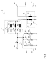
- FIG. 1 illustrates a first example of a transformer arrangement by way of a circuit diagram.
- the transformer arrangement includes a coreless transformer 2 having a primary winding 21 and a secondary winding 22 that are inductively coupled to each other.
- Primary winding 21 has a parasitic capacitance 23 that lies parallel to primary winding 21 .
- parasitic capacitance 23 is shown in dashed lines in FIG. 1 and has reference number 23 .
- Coreless transformer 2 may be any kind of coreless transformer, including a coreless transformer having its primary and secondary windings disposed on a printed circuit board (PCB), or a coreless transformer having its primary and secondary windings integrated in or disposed on a semiconductor chip.
- the transformer arrangement further comprises input terminals 11 , 12 for applying an input voltage Vin, and output terminals 13 , 14 for providing an output voltage Vout.
- One of the input terminals e.g., second input terminal 12 in the example according to FIG. 1
- One of the output terminals e.g., the second output terminal 14 in the example according to FIG. 1
- is connected to a terminal for a second reference potential which will be referred to as secondary-side reference potential in the following.
- the transformer arrangement further comprises a trimming circuit 3 that is connected between input terminals 11 , 12 and primary winding 21 .
- Trimming circuit 3 includes at least one of: an adjustable inductance unit 4 that has an adjustable inductivity and that is connected in series to primary winding 21 ; and an adjustable capacitance unit 5 that has an adjustable capacity and that is connected in parallel to primary winding 21 .
- Adjustable capacitance unit 5 may be connected (as shown) in parallel to a series circuit comprising adjustable inductance unit 4 and primary winding 21 .
- adjustable capacitance unit 5 may also be connected parallel to primary winding 21 , even in those cases in which the transformer arrangement includes adjustable inductance unit 4 .
- the transformer arrangement may include both, adjustable inductance unit 4 and adjustable capacitance unit 5 , or only one of these adjustable units 4 , 5 .
- trimming circuit 3 may also be connected between secondary winding 22 and output terminals 13 , 14 .
- Reference number 24 in FIG. 2 denotes a parasitic capacitance of secondary winding 22 .
- Adjustable inductance unit 4 is in this case connected in series to secondary winding 22
- adjustable capacitance unit 5 is (as shown) connected parallel to the series circuit with secondary winding 22 and adjustable inductance unit 4 .
- adjustable capacitance unit 5 may be connected only in parallel to secondary winding 22 , even in those cases in which the transformer arrangement comprises an adjustable inductance unit 4 .
- the transformer arrangement is adapted to have a driver circuit 10 (shown in dashed lines) connected to its input terminals 11 , 12 , and to have a load circuit 20 connected to its output terminals 13 , 14 .
- driver circuit 10 generates an input voltage Vin at the input terminals 11 , 12 of the transformer arrangement from which the transformer arrangement generates an output voltage Vout at its output terminals 13 , 14 .
- the input voltage Vin is an oscillating or alternating voltage.
- the output voltage Vout is an oscillating or alternating voltage.
- coreless transformer 2 may be described by way of an equivalent circuit diagram.
- Vin′ is a voltage applied to the primary winding 21
- Vout′ is a voltage resulting from input voltage Vin′ across secondary winding 22 .
- FIG. 3 shows the equivalent circuit diagram for the specific case in which a primary reference potential corresponds to a secondary reference potential.
- Reference numbers 25 and 26 in FIG. 3 denote input and output terminals of the coreless transformers. These terminals are also shown in FIG. 1 .
- electrical characteristics of the coreless transformers 2 depend on the following: an input capacitance C p that is connected parallel to the input terminals of coreless transformers 2 ; an output capacitance C S that is connected between the output terminals of coreless transformer 2 ; a coupling capacitance C ps that is connected between one of the input terminals and one of the output terminals of coreless transformer 2 ; ohmic resistance R p of primary winding 21 ; a primary leakage inductance L p ; a secondary leakage inductance L s ; an ohmic resistance R s of secondary winding; and a primary mutual inductance L ps .
- These electrical parameters define the electrical characteristics of coreless transformer 2 .
- These electrical characteristics for example, are: an input impedance Zin′, with:
- a further important electrical characteristic of coreless transformer 2 is its power efficiency ⁇ that is given by:
- coreless transformer 2 Further electrical characteristics of coreless transformer 2 are its maximum impedance frequency (MIF) and its maximum efficiency frequency (MEF).
- MIF maximum impedance frequency
- MEF maximum efficiency frequency
- the maximum impedance frequency is the frequency of input voltage Vin′ for which input impedance Zin′ of coreless transformer 2 reaches its maximum.
- the maximum efficiency frequency is the frequency of the input voltage Vin′ of coreless transformer 2 for which power transfer efficiency l reaches its maximum.
- MIF and MEF depend on the load that is connected to the output terminals of coreless transformer 2 .
- Trimming circuit 3 that, referring to FIGS. 1 and 2 , is either connected to primary winding 21 or to secondary winding 22 serves to compensate for such variations in the electrical characteristics of the coreless transformer 2 .
- Zin Vin Iin , ⁇ and ( 6 )
- Zout Vout Iout , ( 7 )
- the transformer arrangement as a whole like the coreless transformer 2 , has a maximum impedance frequency (MIF) and a maximum efficiency frequency (MEF).
- MIF maximum impedance frequency
- MEF maximum efficiency frequency
- trimming circuit 3 serves to compensate for variations in the electrical characteristics of coreless transformer 2 in order to set the MIF or the MEF of the transformer arrangement to a given frequency value or at least close to a given frequency value.
- This given frequency value is, for example, the frequency of the input voltage Vin provided by driver stage 10 .
- Setting MEF or MIF “close to a given frequency” means that MEF or MIF differs less than a given frequency difference from the given frequency. This difference is, for example, less than about 10% or less than about 5% of the given frequency.
- Trimming circuit 3 is adapted to adjust the electrical characteristic of the transformer arrangement having a coreless transformer 2 .
- Transformer arrangements that have coreless transformers 2 with different electrical characteristics can, using the trimming circuit 3 , be adjusted to have identical or almost identical electrical characteristics and can therefore be driven using identical driver stages 10 .
- trimming circuit 3 trims the transformer arrangement to have either its MIF or to have its MEF at the given frequency is dependent on a specific application of the transformer arrangement. In applications in which the transformer arrangement serves to transfer power, trimming circuit 3 may adjust the MEF to the given frequency; and in applications in which the transformer arrangement is used to transmit information as well as in applications in which the input impedance should be as high as possible, trimming circuit 3 adjusts the MIF of the transformer arrangement to the given frequency value.
- FIG. 4 illustrates examples of adjustable inductance and adjustable capacitance circuits 4 , 5 that are suitable for setting electrical characteristics of the transformer arrangement during manufacturing or at the end of manufacturing.
- the adjustable inductance circuit 4 includes a number of series circuits each of which comprising an inductance 42 1 , 42 2 , 42 n and a fuse 41 1 , 41 2 , 41 n , A further fuse 41 0 directly connects input terminal 11 and primary winding 21 .
- the adjustable inductance circuit 4 has its lowest inductance in case further fuse 41 0 is conducting.
- the fuses 41 0 - 41 n may be any kind of fuses, in particular, fuses that can be manufactured with processes that are used for producing semiconductor components.
- the overall inductance of adjustable inductance circuit 4 can be set by selectively melting the fuses during manufacturing or at the end of manufacturing of the transformer arrangement.
- Adjustable capacitance circuit 5 has a number of series circuits each of which comprising a capacitance 52 1 , 52 2 , 52 n that is connected in series to a fuse 51 1 , 51 2 , 51 n , the series circuits being connected in parallel to each other.
- the overall capacitance of adjustable capacitance circuit 5 is set by selectively melting the fuses 51 1 , 51 2 , 51 n during manufacturing or at the end of manufacturing the transformer arrangement.
- the overall inductance of adjustable inductance circuit 4 and/or the overall capacitance of adjustable capacitance circuit 5 influence the electrical characteristics of the transformer arrangement.
- the electrical characteristics of coreless transformer 2 are measured at the end of the manufacturing process. For example, the MEF and the MIF of coreless transformer 2 is evaluated.
- a difference between the measured MIF or MEF of coreless transformer 2 and a desired MEF or MIF of the transformer arrangement is determined and the inductance value of adjustable inductance 4 and/or the capacitance value of adjustable capacitance value 5 are selected so as to compensate for this difference, wherein MEF or MIF of the transformer arrangement corresponds to MEF or MIF of coreless transformer 2 , if fuse 41 0 of inductance circuit 4 is conducting, and if all fuses 51 1 - 51 n of capacitance circuit 5 have been melted or blown.
- MEF and MIF of coreless transformer 2 due to process variations may vary.
- a maximum variation of this MEF or MIF is defined, where coreless transformers 2 having a MEF or MIF being outside this defined range will be discarded.
- settings for inductance circuit 4 and/or capacitance circuit 5 that are required to set MIF or MEF of the transformer arrangement to a given value can be obtained by simulations or tests. Using such simulations or tests a look-up table can be generated that to each MIF or MEF value, that is within the given range, assigns setting parameters for inductance circuit 4 and/or capacitance circuit 5 .
- MEF 2 , MIF 2 denote measured MEF/MIF values of coreless transformer 2 .
- P 4 , P 5 are setting parameters of inductance circuit 4 and capacitance circuit 5 that considering the measured MEF/MIF values are used for setting MEF/MIF of the transformer arrangement to the desired value MEF D /MIF D .
- MEF 2L /MIF 2L and MEF 2H /MIF 2H denote lower and upper borders of the MEF/MIF range of coreless transformer 2 . For a number of MEF/MIF values of this range setting parameters P 4 , P 5 have been obtained by simulations or tests.
- FIG. 6 illustrates an example of a transformer arrangement in which instead of fuses, switches 43 1 , 43 2 , 43 m are connected in series to inductances 42 1 - 42 n of inductance circuit 4 . Further, a switch 43 0 is connected between input terminal 11 and primary winding 21 . Similarly, instead of fuses, switches 53 1 , 53 2 , 53 n are connected in series to capacitance 52 1 , 52 2 , 52 n of capacitance circuit 5 . Each of these switches receives a control signal S 43 0 -S 43 m , S 53 1 -S 53 n .
- control signals have one of either an on-level or off-level, an on-level of a control signal switching on the respective switch that receives the control signal, and an off-level of the control signal switches the respective switch off.
- a control circuit 6 generates these control signals S 43 0 -S 43 m , S 53 1 -S 53 n .
- the signal levels of control signals S 43 0 -S 43 m form a set of parameters P 4 for adjusting the inductivity of inductance circuit 4
- the signal levels of control signals S 53 1 -S 53 n form a set of parameters P 5 for adjusting the capacity of capacitance circuit 5 .
- the functionality of inductance and capacitance circuits 4 , 5 of FIG. 6 correspond to the functionality of inductance and capacitance circuits 4 , 5 of FIG. 5 with the difference that the inductivity and the capacity of inductance and capacitance circuit 4 , 5 are set electrically using the control signals.
- the different inductances 42 1 , 42 2 , 42 n and the different capacities 52 1 , 52 2 , 52 n may have the same inductivities and capacities.
- the overall inductivity of inductance circuit 4 and the overall capacity of capacitance circuit 5 is set by the number of inductances and capacitances that are connected in parallel.
- the inductances and capacitances have different inductivities and capacities.
- the overall inductivity of inductance circuit 4 and the overall capacity of capacitance circuit 5 can be set by either activating only one of these inductances/capacitances or by activating two or more inductances/capacitances.
- control circuit 6 may comprise a programmable circuit 61 , like an EPROM, or an EEPROM.
- Control circuit 6 further comprises a driver circuit 62 that is connected to programmable circuit 61 and that is adapted to read parameters stored in the programmable circuit 61 and to generate the control signals for inductance and capacitance circuits 4 , 5 dependent on these parameters.
- S 43 , S 53 in FIG. 7 denote the group of control signals provided to inductance circuit 4 , and the group of control signals provided to capacitance circuit 5 .
- Programmable circuit 61 can be programmed at the end of the manufacturing process and after MEF/MIF of coreless transformer 2 has been measured. Programmable circuit 61 after programming holds a set of parameters. These parameters determine the overall inductivity/capacity of inductance circuit 4 and capacitance circuit 5 and correspond to the parameters P 4 , P 5 of FIG. 5 . These parameters set the overall inductivity/capacity of inductance circuit 4 /capacitance circuit 5 such that, considering the measured MEF, MIF of coreless transformer 2 , MEF/MIF of the transformer arrangement corresponds to the desired value MEF D /MIF D .
- MEF and MIF of the transformer arrangement depends on the load connected to output terminals 13 , 14 during operation of the transformer arrangement.
- several sets of parameters are stored in programmable circuit 61 , with each of these different sets of parameters being assigned to one particular load characteristic.
- Each of these parameter sets considers the measured MEF/MIF of coreless transformer 2 and is adapted to adjust the inductivity/capacity of inductance circuit 4 /capacitance circuit 5 such that MEF/MIF of the transformer arrangement corresponds to a given value for a given load characteristic.
- Driver circuit 62 selects one of these parameter sets for generating the control signals S 43 , S 53 dependent on a load signal S LOAD , this load signal S LOAD including an information of the load characteristic of a load to be connected to output terminals 13 , 14 .
- Load signal S LOAD may be generated by any suitable circuit, in particular, by a passive circuit component (not shown) connected to the input terminal of control circuit 6 .
- control signal S LOAD a user may adapt transformer arrangement to be used in connection with different loads having different load characteristics.
- FIG. 8 illustrates another example of a method for trimming the transformer arrangement.
- load characteristic signal S LOAD is generated during operation of the transformer arrangement. This allows to adapt the transfer characteristic of the transformer arrangement to variations in the load.
- An evaluation circuit 7 provides load characteristic signal S LOAD .
- Evaluation circuit 7 which is only shown schematically in FIG. 8 is adapted to evaluate the output impedance Z OUT or the output power of the transformer arrangement, and is adapted to generate load characteristic signal S LOAD dependent on these measured output impedance or output power values.
- the evaluation circuit 7 For determining the output power Pout the evaluation circuit 7 measures the output voltage Vout and one of the following: output current lout, i.e., the current through secondary winding 22 ; or the input current Iin.
- MEF of the transformer arrangement or MIF of the transformer arrangement are measured, a measurement value indicating a current MEF/MIF value is provided to control circuit 6 , control circuit 6 being adapted to adjust inductance circuit 4 and capacitance circuit 5 to set MEF/MIF to a given value.
- the circuit arrangement may comprise a trimmable oscillator circuit 10 that receives a trimming signal S T for trimming an oscillator frequency to a frequency that corresponds to MEF/MIF of the transformer arrangement.
- the function of trimming signal S T corresponds to the function of setting signals P 4 , P 5 that set the characteristic of adjustable inductance and capacitance circuits 4 , 5 . Trimming signal S T may therefore be generated in an equivalent manner as these setting parameters.
- Oscillator circuit 10 further receives an input signal Sin that, for example, serves to activate or deactivate oscillator circuit 10 .
- Input signal Sin may be a pulsewidth-modulated signal that is modulated in accordance with an information signal in order to transmit information via coreless transformer 2 .
Landscapes
- Engineering & Computer Science (AREA)
- Power Engineering (AREA)
- Coils Or Transformers For Communication (AREA)
Abstract
Description
wherein Vin′ is an input voltage and Iin′ is an input current resulting from the input voltage Vin′; input power Pin′ with:
Pin′=Vin′·Iin′ (2),
wherein Vout′ is an output voltage and lout′ is an output current; or output power Pout′ with:
Pout′=Vout′·Iout′ (4).
and input and output power Pin, Pout with:
Pin=Vin·Iin (8),
Pout=Vout·Iout (9),
may be defined for the transformer arrangement. Further, the transformer arrangement as a whole, like the
Claims (15)
Priority Applications (2)
| Application Number | Priority Date | Filing Date | Title |
|---|---|---|---|
| US12/400,141 US9117586B2 (en) | 2009-03-09 | 2009-03-09 | Trimmable transformer arrangement |
| DE201010002711 DE102010002711A1 (en) | 2009-03-09 | 2010-03-09 | Adjustable transformer arrangement |
Applications Claiming Priority (1)
| Application Number | Priority Date | Filing Date | Title |
|---|---|---|---|
| US12/400,141 US9117586B2 (en) | 2009-03-09 | 2009-03-09 | Trimmable transformer arrangement |
Publications (2)
| Publication Number | Publication Date |
|---|---|
| US20100226064A1 US20100226064A1 (en) | 2010-09-09 |
| US9117586B2 true US9117586B2 (en) | 2015-08-25 |
Family
ID=42678082
Family Applications (1)
| Application Number | Title | Priority Date | Filing Date |
|---|---|---|---|
| US12/400,141 Expired - Fee Related US9117586B2 (en) | 2009-03-09 | 2009-03-09 | Trimmable transformer arrangement |
Country Status (2)
| Country | Link |
|---|---|
| US (1) | US9117586B2 (en) |
| DE (1) | DE102010002711A1 (en) |
Families Citing this family (3)
| Publication number | Priority date | Publication date | Assignee | Title |
|---|---|---|---|---|
| US8787999B2 (en) * | 2011-04-15 | 2014-07-22 | Varian Semiconductor Equipment Associates, Inc. | Fault current limited system with current splitting device |
| DE102012113043A1 (en) * | 2012-12-21 | 2014-06-26 | Endress + Hauser Conducta Gesellschaft für Mess- und Regeltechnik mbH + Co. KG | System for contact-less energy and data transfer between primary winding and secondary winding, has resonant circuit whose resonant frequency is changed by directly switching-on and/or switching-off of individual branches by switching unit |
| US10437304B2 (en) * | 2016-03-15 | 2019-10-08 | Roku, Inc. | Brown out condition detection and device calibration |
Citations (8)
| Publication number | Priority date | Publication date | Assignee | Title |
|---|---|---|---|---|
| DE4438287C1 (en) | 1994-10-26 | 1996-05-09 | Siemens Ag | System for contactless energy and data transmission |
| US5953642A (en) * | 1994-10-26 | 1999-09-14 | Siemens Aktiengesellschaft | System for contactless power and data transmission |
| EP0935263B1 (en) | 1998-02-05 | 2004-05-26 | City University of Hong Kong | Method of operating a coreless printed-circuit-board (PCB) transformer |
| US20040130916A1 (en) * | 1999-06-21 | 2004-07-08 | Baarman David W. | Adaptive inductive power supply |
| US20050156699A1 (en) | 1998-02-05 | 2005-07-21 | City University Of Hong Kong | Coreless printed-circuit-board (PCB) transformers and operating techniques therefor |
| US20080231211A1 (en) | 2007-03-20 | 2008-09-25 | Access Business Group International Llc | Power supply |
| US20090033440A1 (en) * | 2007-07-30 | 2009-02-05 | Renesas Technology Corp. | Active resonant circuit with resonant-frequency tunability |
| US8218810B1 (en) * | 2006-07-19 | 2012-07-10 | Stanley Security Solutions, Inc. | Signaling device |
-
2009
- 2009-03-09 US US12/400,141 patent/US9117586B2/en not_active Expired - Fee Related
-
2010
- 2010-03-09 DE DE201010002711 patent/DE102010002711A1/en not_active Withdrawn
Patent Citations (10)
| Publication number | Priority date | Publication date | Assignee | Title |
|---|---|---|---|---|
| DE4438287C1 (en) | 1994-10-26 | 1996-05-09 | Siemens Ag | System for contactless energy and data transmission |
| US5953642A (en) * | 1994-10-26 | 1999-09-14 | Siemens Aktiengesellschaft | System for contactless power and data transmission |
| EP0935263B1 (en) | 1998-02-05 | 2004-05-26 | City University of Hong Kong | Method of operating a coreless printed-circuit-board (PCB) transformer |
| US20050156699A1 (en) | 1998-02-05 | 2005-07-21 | City University Of Hong Kong | Coreless printed-circuit-board (PCB) transformers and operating techniques therefor |
| US7768371B2 (en) * | 1998-02-05 | 2010-08-03 | City University Of Hong Kong | Coreless printed-circuit-board (PCB) transformers and operating techniques therefor |
| US20040130916A1 (en) * | 1999-06-21 | 2004-07-08 | Baarman David W. | Adaptive inductive power supply |
| US8218810B1 (en) * | 2006-07-19 | 2012-07-10 | Stanley Security Solutions, Inc. | Signaling device |
| US20080231211A1 (en) | 2007-03-20 | 2008-09-25 | Access Business Group International Llc | Power supply |
| US8223508B2 (en) * | 2007-03-20 | 2012-07-17 | Access Business Group International Llc | Power supply |
| US20090033440A1 (en) * | 2007-07-30 | 2009-02-05 | Renesas Technology Corp. | Active resonant circuit with resonant-frequency tunability |
Non-Patent Citations (2)
| Title |
|---|
| Qingxin Yang, Jiangui Li, Haiyan Chen and Junhua Wang; "Design and Analysis of New Detachable Coreless Transformer Used for Contact-less Electrical Energy Transmission System"; IEEE Vehicle Power and Propulsion Confrence; Sep. 3-5, 2008; pp. 1-4. * |
| Uno, T., et al., A New Digital TCXO Circuit Using a Capacitor-Switch Array, Musashino Electrical Communication Laboratory, Nippon Telegraph and Telephone Public Corporation,1983, pp. 434-441, IEEE. |
Also Published As
| Publication number | Publication date |
|---|---|
| DE102010002711A1 (en) | 2010-11-25 |
| US20100226064A1 (en) | 2010-09-09 |
Similar Documents
| Publication | Publication Date | Title |
|---|---|---|
| EP2651032B1 (en) | Tunable capacitor | |
| EP2547000B1 (en) | Signal transmitting apparatus | |
| US7460604B2 (en) | RF isolator for isolating voltage sensing and gate drivers | |
| US9711436B2 (en) | Multi chip module, method for operating the same and DC/DC converter | |
| TWI539464B (en) | Method and apparatus for reading a programmable anti-fuse element in a high-voltage integrated circuit | |
| US20060197642A1 (en) | Variable inductor technique | |
| WO2005122423A2 (en) | Spread spectrum isolator | |
| CN104054229A (en) | Wireless power receiver system | |
| CN101854126A (en) | Compensation method and circuit | |
| US9117586B2 (en) | Trimmable transformer arrangement | |
| US20150263184A1 (en) | Photocoupler | |
| US8547132B2 (en) | Circuit board and method for testing component built in the circuit board | |
| US6646450B2 (en) | Method and apparatus for near losslessly measuring inductor current | |
| US10608628B2 (en) | Drive circuit for a transistor component | |
| US8599580B2 (en) | Buck converter | |
| WO2015104769A1 (en) | Circuit constant variable circuit | |
| KR101629964B1 (en) | Power semiconductor module with control functionality and integrated transformer | |
| AU2016278682A1 (en) | Switch apparatus, test apparatus and method for operating a switch apparatus for a measuring device for a transformer | |
| US10014810B1 (en) | Reduced-impedance active current measurement | |
| US20070103187A1 (en) | Impedance circuit, power supply device | |
| Bergogne et al. | Integrated coreless transformer for high temperatures design and evaluation | |
| CN112014616B (en) | Current detection apparatus and method | |
| US10666149B2 (en) | Control circuit for switching power supply | |
| US20060164869A1 (en) | Inverter | |
| EP2335315B1 (en) | Antenna with a controllable switching element connecting two antenna portions |
Legal Events
| Date | Code | Title | Description |
|---|---|---|---|
| AS | Assignment |
Owner name: INFINEON TECHNOLOGIES AUSTRIA AG, AUSTRIA Free format text: ASSIGNMENT OF ASSIGNORS INTEREST;ASSIGNORS:MCCONNELL, RODERICK;STRZALKOWSKI, BERNHARD;SIGNING DATES FROM 20090320 TO 20090403;REEL/FRAME:022515/0661 |
|
| STCF | Information on status: patent grant |
Free format text: PATENTED CASE |
|
| FEPP | Fee payment procedure |
Free format text: PAYOR NUMBER ASSIGNED (ORIGINAL EVENT CODE: ASPN); ENTITY STATUS OF PATENT OWNER: LARGE ENTITY |
|
| FEPP | Fee payment procedure |
Free format text: MAINTENANCE FEE REMINDER MAILED (ORIGINAL EVENT CODE: REM.); ENTITY STATUS OF PATENT OWNER: LARGE ENTITY |
|
| LAPS | Lapse for failure to pay maintenance fees |
Free format text: PATENT EXPIRED FOR FAILURE TO PAY MAINTENANCE FEES (ORIGINAL EVENT CODE: EXP.); ENTITY STATUS OF PATENT OWNER: LARGE ENTITY |
|
| STCH | Information on status: patent discontinuation |
Free format text: PATENT EXPIRED DUE TO NONPAYMENT OF MAINTENANCE FEES UNDER 37 CFR 1.362 |
|
| FP | Lapsed due to failure to pay maintenance fee |
Effective date: 20190825 |