EP2651032B1 - Tunable capacitor - Google Patents
Tunable capacitor Download PDFInfo
- Publication number
- EP2651032B1 EP2651032B1 EP13161526.2A EP13161526A EP2651032B1 EP 2651032 B1 EP2651032 B1 EP 2651032B1 EP 13161526 A EP13161526 A EP 13161526A EP 2651032 B1 EP2651032 B1 EP 2651032B1
- Authority
- EP
- European Patent Office
- Prior art keywords
- terminal
- capacitor
- variable capacitor
- switching transistor
- tunable
- Prior art date
- Legal status (The legal status is an assumption and is not a legal conclusion. Google has not performed a legal analysis and makes no representation as to the accuracy of the status listed.)
- Active
Links
- 239000003990 capacitor Substances 0.000 title claims description 281
- 239000004065 semiconductor Substances 0.000 claims description 16
- 238000010586 diagram Methods 0.000 description 14
- 238000000034 method Methods 0.000 description 5
- 230000000694 effects Effects 0.000 description 4
- 238000004519 manufacturing process Methods 0.000 description 3
- 230000015556 catabolic process Effects 0.000 description 2
- 239000004020 conductor Substances 0.000 description 1
- 238000006731 degradation reaction Methods 0.000 description 1
- 238000013461 design Methods 0.000 description 1
- 230000002708 enhancing effect Effects 0.000 description 1
- 230000001939 inductive effect Effects 0.000 description 1
- 238000012986 modification Methods 0.000 description 1
- 230000004048 modification Effects 0.000 description 1
- 238000012545 processing Methods 0.000 description 1
- 230000035945 sensitivity Effects 0.000 description 1
- 230000008054 signal transmission Effects 0.000 description 1
- 230000002311 subsequent effect Effects 0.000 description 1
- 238000012360 testing method Methods 0.000 description 1
- 238000012546 transfer Methods 0.000 description 1
Images


Classifications
-
- H—ELECTRICITY
- H03—ELECTRONIC CIRCUITRY
- H03K—PULSE TECHNIQUE
- H03K17/00—Electronic switching or gating, i.e. not by contact-making and –breaking
- H03K17/51—Electronic switching or gating, i.e. not by contact-making and –breaking characterised by the components used
- H03K17/56—Electronic switching or gating, i.e. not by contact-making and –breaking characterised by the components used by the use, as active elements, of semiconductor devices
- H03K17/687—Electronic switching or gating, i.e. not by contact-making and –breaking characterised by the components used by the use, as active elements, of semiconductor devices the devices being field-effect transistors
-
- H—ELECTRICITY
- H03—ELECTRONIC CIRCUITRY
- H03H—IMPEDANCE NETWORKS, e.g. RESONANT CIRCUITS; RESONATORS
- H03H7/00—Multiple-port networks comprising only passive electrical elements as network components
- H03H7/38—Impedance-matching networks
-
- H—ELECTRICITY
- H01—ELECTRIC ELEMENTS
- H01G—CAPACITORS; CAPACITORS, RECTIFIERS, DETECTORS, SWITCHING DEVICES OR LIGHT-SENSITIVE DEVICES, OF THE ELECTROLYTIC TYPE
- H01G7/00—Capacitors in which the capacitance is varied by non-mechanical means; Processes of their manufacture
-
- H—ELECTRICITY
- H01—ELECTRIC ELEMENTS
- H01L—SEMICONDUCTOR DEVICES NOT COVERED BY CLASS H10
- H01L23/00—Details of semiconductor or other solid state devices
- H01L23/58—Structural electrical arrangements for semiconductor devices not otherwise provided for, e.g. in combination with batteries
- H01L23/64—Impedance arrangements
- H01L23/642—Capacitive arrangements
-
- H—ELECTRICITY
- H01—ELECTRIC ELEMENTS
- H01L—SEMICONDUCTOR DEVICES NOT COVERED BY CLASS H10
- H01L23/00—Details of semiconductor or other solid state devices
- H01L23/58—Structural electrical arrangements for semiconductor devices not otherwise provided for, e.g. in combination with batteries
- H01L23/64—Impedance arrangements
- H01L23/66—High-frequency adaptations
-
- H—ELECTRICITY
- H01—ELECTRIC ELEMENTS
- H01L—SEMICONDUCTOR DEVICES NOT COVERED BY CLASS H10
- H01L27/00—Devices consisting of a plurality of semiconductor or other solid-state components formed in or on a common substrate
- H01L27/02—Devices consisting of a plurality of semiconductor or other solid-state components formed in or on a common substrate including semiconductor components specially adapted for rectifying, oscillating, amplifying or switching and having at least one potential-jump barrier or surface barrier; including integrated passive circuit elements with at least one potential-jump barrier or surface barrier
- H01L27/0203—Particular design considerations for integrated circuits
- H01L27/0248—Particular design considerations for integrated circuits for electrical or thermal protection, e.g. electrostatic discharge [ESD] protection
- H01L27/0251—Particular design considerations for integrated circuits for electrical or thermal protection, e.g. electrostatic discharge [ESD] protection for MOS devices
-
- H—ELECTRICITY
- H01—ELECTRIC ELEMENTS
- H01L—SEMICONDUCTOR DEVICES NOT COVERED BY CLASS H10
- H01L29/00—Semiconductor devices adapted for rectifying, amplifying, oscillating or switching, or capacitors or resistors with at least one potential-jump barrier or surface barrier, e.g. PN junction depletion layer or carrier concentration layer; Details of semiconductor bodies or of electrodes thereof ; Multistep manufacturing processes therefor
- H01L29/66—Types of semiconductor device ; Multistep manufacturing processes therefor
- H01L29/86—Types of semiconductor device ; Multistep manufacturing processes therefor controllable only by variation of the electric current supplied, or only the electric potential applied, to one or more of the electrodes carrying the current to be rectified, amplified, oscillated or switched
- H01L29/92—Capacitors with potential-jump barrier or surface barrier
- H01L29/93—Variable capacitance diodes, e.g. varactors
-
- H—ELECTRICITY
- H03—ELECTRONIC CIRCUITRY
- H03H—IMPEDANCE NETWORKS, e.g. RESONANT CIRCUITS; RESONATORS
- H03H11/00—Networks using active elements
- H03H11/02—Multiple-port networks
- H03H11/28—Impedance matching networks
-
- H—ELECTRICITY
- H01—ELECTRIC ELEMENTS
- H01L—SEMICONDUCTOR DEVICES NOT COVERED BY CLASS H10
- H01L2223/00—Details relating to semiconductor or other solid state devices covered by the group H01L23/00
- H01L2223/58—Structural electrical arrangements for semiconductor devices not otherwise provided for
- H01L2223/64—Impedance arrangements
- H01L2223/66—High-frequency adaptations
- H01L2223/6644—Packaging aspects of high-frequency amplifiers
- H01L2223/6655—Matching arrangements, e.g. arrangement of inductive and capacitive components
-
- H—ELECTRICITY
- H01—ELECTRIC ELEMENTS
- H01L—SEMICONDUCTOR DEVICES NOT COVERED BY CLASS H10
- H01L2924/00—Indexing scheme for arrangements or methods for connecting or disconnecting semiconductor or solid-state bodies as covered by H01L24/00
- H01L2924/0001—Technical content checked by a classifier
- H01L2924/0002—Not covered by any one of groups H01L24/00, H01L24/00 and H01L2224/00
Definitions
- the present invention relates to a tunable capacitor capable of tuning a capacitance, and more particularly to a tunable capacitor which is integrated on one semiconductor die.
- a radio frequency integrated circuit may use an impedance matching circuit for interfacing mutually different sections within an RFIC network.
- the impedance matching circuit improves power transfer among the sections or reduces signal reflections occurring among respective sections.
- a tuning matching network is employed for the purpose of enhancing such an impedance matching performance. This is a significant issue in a circuit design.
- EP 1 365 507 A1 discloses a universal tuning and matching device for high frequency or radio frequency signal transmission systems and/or applications where within one IC package at least two capacitors and two inductors, at least one signal path with at least one input and output port and controllable switching means for individually connecting and disconnecting at least one of the capacitors and/or at least one of the conductors into the signal path or from the signal path are provided.
- One of the capacitors is a varactor, i.e., is tunable, and one of the inductors is a variometer, i.e., is also tunable.
- the other capacitors and inductors are fixed.
- One embodiment is a tunable capacitor including a tuning switch which on/off controls a connection between a variable capacitor unit and an impedance tuner connected in parallel to at least one of both terminals of the variable capacitor unit.
- the impedance tuner is connected between at least one of both terminals of the variable capacitor unit and ground; and the tuning switch on/off controls the connection between the variable capacitor unit and said impedance tuner or between said impedance tuner and ground.
- the variable capacitor unit and the tuning switch are integrated on one semiconductor die.
- the impedance tuner is separate from the semiconductor die, i.e., is not integrated on said semiconductor die.
- the tunable capacitor may further include a bypass switch which on/off controls a bypass connection between the first terminal and the second terminal.
- the variable capacitor unit, the bypass switch and the tuning switch may be integrated on one semiconductor die.
- the variable capacitor unit may include at least one of a variable capacitor of which the capacitance is controlled by current or voltage and a MEMS variable capacitor.
- the variable capacitor unit may include a first capacitor; and a switching transistor which switches on/off the connection of the first capacitor between the first terminal and the second terminal.
- a high signal H may be applied to a gate terminal G, and a low signal L may be applied to a body terminal B, a drain terminal D and a source terminal S.
- the low signal L may be applied to the gate terminal G and the body terminal B, and the high signal H may be applied to the drain terminal D and the source terminal S.
- the switching transistor may be a stacked transistor formed by connecting in series a plurality of transistors.
- the gate terminal G and the body terminal B of the switching transistor may be connected in series to a resistance respectively.
- the first capacitor may be formed by connecting in series or in parallel a plurality of the capacitors.
- An on/off operation of the switching transistor may be performed by a high signal H and a low signal L.
- the tunable capacitor may include a plurality of the variable capacitor units.
- the plurality of the variable capacitor units may be connected in parallel to each other.
- Each of the plurality of the variable capacitor units may include the first capacitor and the switching transistor which switches on/off the connection of the first capacitor between the first terminal and the second terminal.
- An equivalent capacitance of the plurality of the variable capacitor units may be 2 m-1 ⁇ C1 (here, m is a natural number less than n).
- Width-to-length ratios W/L of the switching transistors of the plurality of the variable capacitor units may be 2 m-1 ⁇ W1 (here, m is a natural number less than n) respectively.
- the n may be a number of the variable capacitor units.
- the C1 may be an equivalent capacitance of a particular variable capacitor unit.
- the W1 may be a channel width-to-length ratio W/L of the switching transistor.
- the tunable capacitor may further include a fixed capacitor which is connected in parallel to a plurality of the variable capacitor units.
- the tunable capacitor may further include a controller which receives a digital control signal and controls on/off of the switching transistor.
- An on/off operation of the switching transistor may be performed by a high signal H and a low signal L.
- a positive voltage applied to a transistor is VDD in a case where the transistor is an on-state with regard to a voltage signal applied to the transistor
- a high signal H has a voltage of about VDD/2 to VDD
- a low signal L has a voltage of 0V (i.e., a ground signal) to about VDD/2.
- a standard for dividing the voltage signal applied to the transistor into the high signal H and the low signal L is not necessarily fixed. The standard may be changed according to an implementation environment of the tunable capacitor according to the embodiment of the present invention, for example, a magnitude of the applied positive voltage VDD or the characteristics of the transistor and the like.
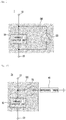
- Fig. 1 is a view showing a tunable capacitor 1 according to a first example.
- the tunable capacitor 1 may include a variable capacitor unit 30 placed between a first terminal 10 and a second terminal 20, and a bypass switch BS which bypasses between the first terminal 10 and the second terminal 20.
- variable capacitor unit 30 of the tunable capacitor 1 are connected to the first terminal 10 and the second terminal 20 respectively.
- the bypass switch BS is connected in parallel to the variable capacitor unit 30 between the first and the second terminals 10 and 20.
- the first terminal 10 may be a load line unit connected to a load.
- the second terminal 20 may be a ground terminal connected to the ground.
- the first terminal 10 may be an RF+ terminal connected to an RF input port.
- the second terminal 20 may be an RF- terminal connected to an RF output port.
- the first and the second terminals 10 and 20 may be used as a terminal having another form by a person having ordinary skill in the art.
- the tunable capacitor 1 has a normal mode and a bypass mode.
- the bypass switch BS receives a control signal and on/off controls the bypass connection between the first terminal 10 and the second terminal 20. That is, when the bypass switch BS becomes in an on-state, the tunable capacitor 1 operates in the bypass mode.
- the first terminal 10 and the second terminal 20 are bypass-connected to each other, so that a signal between the first terminal 10 and the second terminal 20 flows along a bypass path.
- the bypass switch BS becomes in an off-state, the tunable capacitor 1 operates in the normal mode. That is, the bypass path between the first terminal 10 and the second terminal 20 is blocked, so that the signal between the first terminal 10 and the second terminal 20 flows through the variable capacitor unit 30.
- the tunable capacitor 1 since the tunable capacitor 1 according to the first example includes the bypass switch BS between the first terminal 10 and the second terminal 20, it is easy to perform calibration for a circuit, a device or the like which can be connected to the both terminals 10 and 20 of the tunable capacitor 1. In other words, even after the tunable capacitor 1 is integrated on a semiconductor die, etc., it is easy to test or measure in the bypass mode for the purpose of the calibration for circuits, devices and the like other than the variable capacitor unit 30.
- variable capacitor unit 30 is able to control capacitance in accordance with an external control signal.
- the variable capacitor unit 30 according to the embodiment of the present invention may include at least one capacitor which is connected in series or in parallel thereto, and then a corresponding capacitor is selected according to the external control signal.
- the variable capacitor unit 30 according to the embodiment of the present invention is not necessarily limited to this. Any structure capable of controlling the capacitance can be included in the variable capacitor unit 30 of the present invention. A concrete implementation example of the variable capacitor unit 30 will be described later in detail.
- the capacitor unit 30 and the bypass switch BS are integrated on one semiconductor die.
- the tunable capacitor 1 can be implemented as one chip or one module by integrating the capacitor unit 30 and the bypass switch BS on one semiconductor die. By doing this, the number of chips or modules required for implementing the tunable capacitor 1 is reduced. Accordingly, the entire size of the tunable capacitor 1 is reduced. Also, since the tunable capacitor 1 is implemented as one module, the operating speed and reliability of the tunable capacitor 1 are increased. That is, the tunable capacitor 1 is advantageous in space utilization and has a shortened production process. Thus, manufacturing time and manufacturing cost can be reduced. Additionally, the tunable capacitor 1 requires less wiring and becomes smaller, and thus reduces power consumption.
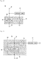
- Figs. 2a and 2b are brief views showing structures of tunable capacitors 2a and 2b accordance with a first embodiment of the present invention.
- the tunable capacitors 2a and 2b may include a variable capacitor unit 30 placed between a first terminal 10 and a second terminal 20, and a tuning switch TS which on/off controls the connection between the variable capacitor unit 30 and an impedance tuner 40 connected in parallel to at least one of both terminals of the variable capacitor unit 30.
- variable capacitor unit 30 is the same as the variable capacitor unit 30 according to the first example shown in Fig. 1 . Therefore, a detailed description thereof will be omitted.
- the tuning switch TS on/off controls the connection between the variable capacitor unit 30 and the impedance tuner 40.
- the impedance tuner 40 can tune the impedance in such a manner as to impedance match a capacitance determined by the variable capacitor unit 30. Therefore, the impedance tuner 40 may include an inductor which is an inductive element and impedance matches the capacitor, i.e., a capacitive element.
- the tuning switch TS on/off controls the connection between the impedance tuner 40 and the tunable capacitors 2a and 2b according to the embodiment of the present invention, so that the impedance matching can be accomplished between the first terminal 10 and the second terminal 20.
- variable capacitor unit 30 and the tuning switch TS are integrated on one semiconductor die or on one module.
- the tunable capacitors 2a and 2b can be implemented as one chip or one module by integrating the capacitor unit 30 and the tuning switch TS on one semiconductor die.
- the effects of the tunable capacitor integrated on one semiconductor die or on one module are the same as those of the first embodiment shown in Fig. 1 . Therefore, a detailed description thereof will be omitted.
- Figs. 2a and 2b show that the impedance tuner 40 is connected between the first terminal 10 and the ground terminal, the impedance tuner 40 is not necessarily limited to this.
- the impedance tuner 40 may be also connected between the second terminal 20 and the ground terminal.
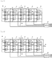
- Figs. 3a and 3b are block diagrams showing tunable capacitors according to the second embodiment of the present invention.
- tunable capacitors 3a and 3b according to the second embodiment may include the bypass switch (BS) described in the first embodiment and the tuning switch TS described in the second embodiment.
- the calibration for circuits, devices or the like connected to the first terminal 10 or the second terminal 20 can be performed by the bypass connection between the first terminal 10 and the second terminal 20.
- the connection between the variable capacitor unit 30 and the impedance tuner 40 can be controlled according to the on/off control of the tuning switch TS.
- Figs. 3a and 3b show that the impedance tuner 40 is connected between the first terminal 10 and the ground terminal, the impedance tuner 40 is not necessarily limited to this.
- the impedance tuner 40 may be also connected between the second terminal 20 and the ground terminal.
- the tunable capacitors 3a and 3b according to the third embodiment are integrated on one semiconductor die. Since subsequent effects to this have been already described in the foregoing first and the second embodiments, detailed descriptions thereof will be omitted.
- variable capacitor unit 30 a concrete implementation example of the variable capacitor unit 30 will be described.
- Fig. 4 shows a variable capacitor unit according to an embodiment of the present invention.
- variable capacitor unit 30 includes a first capacitor 100 placed between the first terminal 10 and the second terminal 20, and a switching transistor 300 which switches on/off the connection of the first capacitor 100 between the first terminal 10 and the second terminal 20.
- first capacitor 100 of the variable capacitor unit 30 are connected to the first terminal 10 and the switching transistor 300 respectively.
- One and the other end of the switching transistor 300 are connected to the first capacitor 100 and the second terminal 20 respectively.
- the switching transistor 300 receives a control signal and controls the on/off of the variable capacitor unit 30 corresponding to the control signal.
- the corresponding variable capacitor unit 30 may or may not be selected between the first terminal 10 and the second terminal 20.
- a variety of semiconductor devices may be used as the switching transistor 300.
- variable capacitor unit may include a variable capacitor of which the capacitance is controlled by current or voltage, or a MEMS variable capacitor manufactured in a micro electro mechanical system (MEMS) manner or may include any combination of them.
- MEMS micro electro mechanical system
- Fig. 5a shows the operation of the variable capacitor unit 30 using a negative voltage.
- a gate-source voltage (VGS) and a gate-drain voltage (VGD) are positive voltages VDD
- a body-source voltage (VBS) and a body-drain voltage (VBD) are 0V
- the gate-source voltage (VGS) and the gate-drain voltage (VGD) are negative voltages -VDD
- the body-source voltage (VBS) and the body-drain voltage (VBD) are also negative voltages -VDD. This intends to improve high power handling capability and linearity of the variable capacitor unit 30.
- a signal of 0V (GND) is applied to a drain terminal D, a source terminal S and a body terminal B of the switching transistor, and a signal of the positive voltage VDD is applied to a gate terminal G.
- the signal of 0V (GND) is applied to the drain terminal D and the source terminal S
- a signal of the negative voltage -VDD is applied to the gate terminal G and the body terminal B. That is, the gate-source voltage (VGS) and the gate-drain voltage (VGD) have a negative value. Therefore, the signal of the negative voltage -VDD is transmitted for the purpose of the on/off operation of the switching transistor 300.
- Fig. 5 shows the on/off state of the switching transistor of the variable capacitor unit which does not use the negative voltage.
- the drain terminal D may be connected to the first capacitor 100, and the source terminal S may be connected to the second terminal 20.
- the switching transistor 300 functions to switch on/off the first capacitor 100. Due to the characteristics of the transistor, the switching transistor 300 may be reversely connected between the first terminal 10 and the second terminal 20. That is, the source terminal S of the switching transistor 300 may be connected to the first capacitor 100, and the drain terminal D may be connected to the second terminal 20.
- the drain terminal D of the switching transistor 300 is connected to the first capacitor 100 will be taken as an example for description.
- the switching transistor 300 when the switching transistor 300 is in the on-state, the high signal H is applied to the gate terminal G, and the low signal L is applied to the drain terminal D, the source terminal S and the body terminal B.
- the low signal L is applied to the gate terminal G and the body terminal B of the switching transistor 300, and the high signal H is applied to the drain terminal D and the source terminal S.
- the operation of the switching transistor 300 according to the embodiment of the present invention is determined by the gate-drain voltage (VGD) of an electric potential difference between the gate terminal G and the drain terminal D, the gate-source voltage (VGS) of an electric potential difference between the gate terminal G and the source terminal S, the body-drain voltage (VBD) of an electric potential difference between the body terminal B and the drain terminal D, and the body-source voltage (VBS) of an electric potential difference between the body terminal B and the source terminal S.
- variable capacitor unit 30 of the tunable capacitor 1 despite the fact that the voltages applied to the respective terminals of the switching transistor 300 which does not use the negative voltage are different from the voltages applied to the respective terminals of the switching transistor which uses the negative voltage, the electric potential differences between the respective terminals are the same as each other, so that the two switching transistors perform the same operation. Accordingly, the tunable capacitor 1 according to the embodiment of the present invention shown in Fig. 5b does not use the negative voltage and is able to maintain the same power handling capability and linearity as those of the tunable capacitor using the negative voltage.
- the tunable capacitor 1 may include the variable capacitor unit using the negative voltage.
- the tunable capacitor 1 should include the variable capacitor unit 30 which has excellent power handling capability and linearity and does not use the negative voltage.
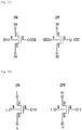
- Fig. 6 shows a variable capacitor unit according to another embodiment of the present invention.
- a switching transistor 300' of the variable capacitor unit 30a may be formed to have a structure in which the plurality of transistors are in series connected.
- a stacked transistor formed by connecting in series the plurality of the transistors instead of a single transistor is advantageous in improving the power handling capability and linearity of the tunable capacitor.
- Control signals applied to the respective transistors are the same as each other and the on/off operations of the respective transistors are performed in the same manner. Since the stacked transistor is a publicly known art, a detailed description thereof will be omitted.
- Fig. 7 shows the variable capacitor unit according to further another embodiment of the present invention.
- a gate terminal G and a body terminal B of the switching transistor 300 may be connected to a first resistance 401 and a second resistance 402 respectively.
- the gate terminal G of the switching transistor 300 of a variable capacitor unit 30b may be connected to the first resistance (R1) 401 and the body terminal B may be connected to the second resistance (R2) 402.
- the first resistance (R1) 401 connected to the gate terminal G and the second resistance (R2) 402 intend to cause the switching transistor 300 to be always in the on-state without being turned off. That is, it is possible to prevent the switching transistor 300 from being in the off-state during the process of swinging an inputted on-signal. Similarly, when an off-signal is inputted, the switching transistor 300 can be prevented from being in the on-state.
- Fig. 8 shows a variable capacitor unit according to yet another embodiment of the present invention.
- a first capacitor 100a has a stacked structure formed by connecting in series the plurality of capacitors.
- a first capacitor 100a of a variable capacitor unit 30c may be a stacked capacitor obtained by connecting in series the capacitors. This intends to enhance an effective breakdown voltage of the capacitor.
- the variable capacitor unit 30c according to the embodiment of the present invention may be used in a smaller and lighter electronic device and the like. Also, the variable capacitor unit 30c is advantageous for processing a radio frequency signal.
- Fig. 9 shows a variable capacitor unit according to still another embodiment of the present invention.
- a first capacitor 100b of a variable capacitor unit 30d has a structure formed by connecting in parallel the plurality of capacitors
- the first capacitor 100b can be implemented by connecting in parallel the plurality of the capacitors. Since the capacitance of the first capacitor 100b is increased due to the parallel connection of the capacitors, a tunable capacitor having a large capacitance can be created.
- variable capacitor unit 30 includes the first capacitor 100 and the switching transistor 300.
- the variable capacitor units 30a and 30b can be implemented by using the stacked transistor as the switching transistor 300 of the variable capacitor unit 30 or by connecting resistances to the gate terminal G and the body terminal B.
- the variable capacitor units 30c and 30d can be implemented by stacking the first capacitors 100 or by connecting in parallel a plurality of the first capacitors 100.
- Fig. 10a is a brief view showing the variable capacitor unit 30 according to the embodiment of the present invention.
- Fig. 10b is a circuit diagram showing the concretely implemented variable capacitor unit 30.
- variable capacitor unit 30 includes the first capacitor 100 placed between the first terminal 10 and the second terminal 20, and the switching transistor 300 which switches on/off the connection of the first capacitor 100 between the first terminal 10 and the second terminal 20.
- the on/off operation of the switching transistor 300 of the variable capacitor unit 30 according to the embodiment of the present invention is performed by the low signal L and the high signal H without using the negative voltage.
- the signal applied to the gate terminal G of the switching transistor 300 is converted, and then the converted signal is applied to the drain terminal D and the source terminal S of the switching transistor 300.
- first capacitor 100 of the variable capacitor unit 30 are connected to the first terminal 10 and the switching transistor 300 respectively.
- One and the other end of the switching transistor 300 are connected to the first capacitor 100 and the second terminal 20 respectively.
- variable capacitor unit 30 may further include a converter 500 which generates a control signal applied to the drain terminal D and the source terminal S of the switching transistor 300.
- the converter 500 converts an input signal applied to the gate terminal G of the switching transistor 300 and applies the converted signal to the drain terminal D and the source terminal S of the switching transistor 300.
- a resistance may be connected in series to the body terminal B and the gate terminal G of the switching transistor 300.
- a third resistance (R3) 403 and a fourth resistance (R4) 404 may be inserted between the converter 500 and both of the drain terminal D and the source terminal S.
- the third resistance (R3) 403 and the fourth resistance (R4) 404 are able to prevent signal loss of the converter.
- the converter 500 converts the voltage respectively applied to the drain terminal D and the source terminal S of the switching transistor 300 and causes the voltage to be opposite to the voltage applied to the gate terminal G.
- An inverter, etc., capable of converting the inputted control signal may be used as the converter 500.
- variable capacitor unit 30 of the tunable capacitor 1 a method for controlling the on/off operation of the first capacitor 100 by the voltage applied to the switching transistor 300 by the converter 500 will be described.
- An external control signal is applied to the respective gate terminals G of the switching transistor 300.
- the control signal is converted by the converter 500 and may be applied to the drain terminal D and the source terminal S of the switching transistor 300.
- the high signal H is applied to the gate terminal G of the switching transistor 300 and the low signal L is applied to the drain terminal D and the source terminal S. Therefore, the gate-source voltage (VGS) and the gate-drain voltage (VGD) have a positive value, so that the switching transistor 300 becomes in the on-state. Accordingly, the first capacitor 100 is selected between the first terminal 10 and the second terminal 20.
- the low signal L is applied to the body terminal B in an on/off state of the on/off switching transistor 300.
- Fig. 10b is a circuit diagram showing the actually implemented variable capacitor unit of Fig. 10a.
- Fig. 10b also shows an example in which the switching transistor 300 is implemented by the stacked transistor.
- variable capacitor unit formed by connecting in parallel a plurality of the variable capacitors.
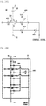
- Fig. 11 is a circuit diagram showing the variable capacitor unit 30 according to an embodiment of the present invention.
- variable capacitor unit 30 may include a plurality of variable capacitors 31, 32, 33, 34 and 35 which are connected in parallel to each other and are placed between the first terminal 10 and the second terminal 20.
- the variable capacitor unit 30 may further include a controller 50 controlling the variable capacitor unit 30.
- variable capacitor unit including five variable capacitors will be described for convenience of description, the number of the variable capacitors connected in parallel may be changed according to the variation range to be implemented of the variable capacitor unit.
- the first terminal 10 may function as an RF+ terminal and the second terminal 20 may function as an RF- terminal.
- variable capacitors 31, 32, 33, 34 and 35 include first capacitors 110, 120, 130, 140 and 150 and switching transistors 310, 320, 330, 340 and 350 respectively.
- capacitances of the first capacitors 110, 120, 130, 140 and 150 of the variable capacitors 31, 32, 33, 34 and 35, channel width-to-length ratios W/L of the switching transistors 310, 320, 330, 340 and 350, gate resistances and body resistances may be set as mutually different values.
- a weight may be applied to the capacitances of the first capacitors 110, 120, 130, 140 and 150, the channel width-to-length ratios W/L of the switching transistors 310, 320, 330, 340 and 350, the gate resistances and the body resistances.
- the weight of the next variable capacitor 32 may be set twice as much as that of the least significant capacitor (LSC) 31.
- LSC least significant capacitor
- the weight becomes twice the capacitance of the first capacitor 120, and the channel width-to-length ratios W/L of the switching transistor 320 become twice as much as the capacitance of the first capacitor 110 of the least significant capacitor (LSC) 31, and the channel width-to-length ratios W/L of the switching transistor 310 respectively.
- the weight of the next variable capacitor 33 may be set four times as much as that of the least significant capacitor (LSC) 31.
- the fifth variable capacitor 35 i.e., the last variable capacitor corresponds to a most significant capacitor (MSC) having the maximum weight.
- the switching transistor 310 of the least significant capacitor (LSC) 31 becomes in the on-state.
- the switching transistors 320, 330, 340 and 350 of the other variable capacitors 32, 33, 34 and 35 become in the off-state. Therefore, the capacitance between the first terminal 10 and the second terminal 20 is varied to the capacitance of the first capacitor 110.
- the capacitance of the least significant capacitor (LSC) 31 is 1pF
- the capacitance of the variable capacitor unit 30 may be variable from minimally 1pF to maximally 31 pF.
- variable capacitor unit 30 when the variable capacitor unit 30 is controlled by the controller 50, digital control signals b0, b1, b2, b3 and b4 are applied to the controller 50, and then the controller 50 may output a control signal corresponding to the digital control signals.
- the variable capacitor unit 30 is able to perform a 5-bit digital control.
- the digital control signals b0, b1, b2, b3 and b4 are changed into the low signal or the high signal, the respective switching transistors 310, 320, 330, 340 and 350 are on/off controlled, so that the tuning may be digitally performed. Therefore, when the number of the variable capacitors is n, the variable capacitor unit 30 is capable of performing n-bit digital tuning operation.
- Fig. 12 shows a variable capacitor unit 30' unit according to another embodiment of the present invention.
- variable capacitor unit 30' may further include a fixed capacitor (Cfixed) 160 added in parallel to the tunable capacitors 31, 32, 33, 34 and 35 which are connected in parallel to each other.
- Cfixed fixed capacitor
- the capacitor between the first terminal 10 and the second terminal 20 may correspond to the fixed capacitor (Cfixed) 160.
- the tunable capacitor includes the variable capacitor unit capable of tuning the capacitance between the first terminal 10 and the second terminal 20 and includes the bypass switch which bypasses between the first terminal 10 and the second terminal 20, so that it is easy to perform calibration for circuits or devices which are connected to the first terminal 10 or the second terminal 20.
- the tunable capacitor includes the variable capacitor unit capable of tuning the capacitance between the first terminal 10 and the second terminal 20 and includes the tuning switch which controls the connection between the variable capacitor unit and the impedance tuner 40 placed between the ground terminal and either the first terminal 10 or the second terminal 20, so that it is possible to efficiently accomplish the impedance matching between the first terminal 10 and the second terminal 20.
- the voltage applied to the gate terminal G of the switching transistor is converted and then is applied to the source terminal S and the drain terminal D, so that it is possible to control the on/off of the switching transistor without generating a separate negative voltage.
- a response becomes faster and more accurate and the negative voltage is not used, and thus a negative voltage generator is not required. Accordingly, it is possible to overcome problems caused by the negative voltage generator, for example, sensitivity degradation, power consumption, space utilization and the like.
Description
- The present invention relates to a tunable capacitor capable of tuning a capacitance, and more particularly to a tunable capacitor which is integrated on one semiconductor die.
- In general, a radio frequency integrated circuit (RFIC) may use an impedance matching circuit for interfacing mutually different sections within an RFIC network. The impedance matching circuit improves power transfer among the sections or reduces signal reflections occurring among respective sections. For the purpose of enhancing such an impedance matching performance, a tuning matching network is employed. This is a significant issue in a circuit design.
- Since parameters of various circuit elements (e.g., inductor, capacitor and the like) depend on many factors, it is difficult to accurately predict the performance of the impedance matching circuit. Therefore, a method has been used, which initially predicts the performance of the impedance matching circuit by using an on-chip circuit element for the purpose of detailed impedance matching, and then determines the validity of the circuit by measuring the result from the initial prediction. However, when the measured result is not satisfied, a new circuit element must be substituted for the circuit element. Therefore, the method is complicated and much process time-consuming. Also, there is a problem that it is difficult to physically replace a circuit element of an integrated circuit placed on a die.
- Accordingly, there is a requirement for a tuning circuit capable of performs calibration or impedance matching without replacing the integrated circuit on the die. Meanwhile, in terms of noise or space, it is urgently required to develop a tunable capacitor which is implemented by a capacitor instead of an inductor and is capable of performing the calibration or impedance matching.
-
EP 1 365 507 A1 - One embodiment is a tunable capacitor including a tuning switch which on/off controls a connection between a variable capacitor unit and an impedance tuner connected in parallel to at least one of both terminals of the variable capacitor unit. I.e., the impedance tuner is connected between at least one of both terminals of the variable capacitor unit and ground; and the tuning switch on/off controls the connection between the variable capacitor unit and said impedance tuner or between said impedance tuner and ground. The variable capacitor unit and the tuning switch are integrated on one semiconductor die. The impedance tuner is separate from the semiconductor die, i.e., is not integrated on said semiconductor die.
- The tunable capacitor may further include a bypass switch which on/off controls a bypass connection between the first terminal and the second terminal. The variable capacitor unit, the bypass switch and the tuning switch may be integrated on one semiconductor die.
- The variable capacitor unit may include at least one of a variable capacitor of which the capacitance is controlled by current or voltage and a MEMS variable capacitor.
- The variable capacitor unit may include a first capacitor; and a switching transistor which switches on/off the connection of the first capacitor between the first terminal and the second terminal.
- When the switching transistor is in the on-state, a high signal H may be applied to a gate terminal G, and a low signal L may be applied to a body terminal B, a drain terminal D and a source terminal S. When the switching transistor is in the off-state, the low signal L may be applied to the gate terminal G and the body terminal B, and the high signal H may be applied to the drain terminal D and the source terminal S.
- The switching transistor may be a stacked transistor formed by connecting in series a plurality of transistors.
- The gate terminal G and the body terminal B of the switching transistor may be connected in series to a resistance respectively.
- The first capacitor may be formed by connecting in series or in parallel a plurality of the capacitors.
- An on/off operation of the switching transistor may be performed by a high signal H and a low signal L.
- The tunable capacitor may include a plurality of the variable capacitor units. The plurality of the variable capacitor units may be connected in parallel to each other. Each of the plurality of the variable capacitor units may include the first capacitor and the switching transistor which switches on/off the connection of the first capacitor between the first terminal and the second terminal.
- An equivalent capacitance of the plurality of the variable capacitor units may be 2m-1×C1 (here, m is a natural number less than n). Width-to-length ratios W/L of the switching transistors of the plurality of the variable capacitor units may be 2m-1×W1 (here, m is a natural number less than n) respectively. The n may be a number of the variable capacitor units. The C1 may be an equivalent capacitance of a particular variable capacitor unit. The W1 may be a channel width-to-length ratio W/L of the switching transistor.
- The tunable capacitor may further include a fixed capacitor which is connected in parallel to a plurality of the variable capacitor units.
- The tunable capacitor may further include a controller which receives a digital control signal and controls on/off of the switching transistor.
- An on/off operation of the switching transistor may be performed by a high signal H and a low signal L.
-
-
Fig. 1 is a brief view showing a structure of a tunable capacitor including a bypass switch in accordance with a first example, not covered by the scope of the present invention; -
Figs. 2a and2b are brief views showing structures of tunable capacitors including an impedance tuner accordance with a first embodiment of the present invention; -
Figs. 3a and3b are block diagrams showing structures of tunable capacitors including a bypass switch and an impedance tuner according to a second embodiment of the present invention; -
Fig. 4 is a circuit diagram showing a tunable capacitor according to an embodiment of the present invention; -
Fig. 5a is a brief view showing a variable capacitor unit which uses a negative voltage, andFig. 5b is a brief view showing a variable capacitor unit which does not use the negative voltage; -
Fig. 6 is a circuit diagram showing a variable capacitor unit according to another embodiment of the present invention; -
Fig. 7 is a circuit diagram showing a variable capacitor unit according to further another embodiment of the present invention; -
Fig. 8 is a circuit diagram showing a variable capacitor unit according to yet another embodiment of the present invention; -
Fig. 9 is a circuit diagram showing a variable capacitor unit according to still another embodiment of the present invention; -
Fig. 10a is a circuit diagram showing the variable capacitor unit according to an embodiment of the present invention, andFig. 10b is a circuit diagram showing the implemented variable capacitor unit; -
Fig. 11 is a circuit diagram showing a variable capacitor unit according to an embodiment of the present invention; and -
Fig. 12 is a circuit diagram showing a variable capacitor unit according to another embodiment of the present invention. - The following detailed description of the present invention shows a specified embodiment of the present invention and will be provided with reference to the accompanying drawings. The embodiment will be described in enough detail that those skilled in the art are able to embody the present invention. It should be understood that various embodiments of the present invention are different from each other and need not be mutually exclusive. For example, a specific shape, structure and properties, which are described in this disclosure, may be implemented in other embodiments without departing from the spirit and scope of the present invention with respect to one embodiment. Also, it should be noted that positions or placements of individual components within each disclosed embodiment may be changed without departing from the spirit and scope of the present invention. Therefore, the following detailed description is not intended to be limited. If adequately described, the scope of the present invention is limited only by the appended claims of the present invention as well as all equivalents thereto. Similar reference numerals in the drawings designate the same or similar functions in many aspects.
- Prior to the description of a tunable capacitor according to an embodiment of the present invention, when it is assumed that a positive voltage applied to a transistor is VDD in a case where the transistor is an on-state with regard to a voltage signal applied to the transistor, it means that a high signal H has a voltage of about VDD/2 to VDD and a low signal L has a voltage of 0V (i.e., a ground signal) to about VDD/2. A standard for dividing the voltage signal applied to the transistor into the high signal H and the low signal L is not necessarily fixed. The standard may be changed according to an implementation environment of the tunable capacitor according to the embodiment of the present invention, for example, a magnitude of the applied positive voltage VDD or the characteristics of the transistor and the like.
- Hereafter, a tunable capacitor according to a first example outside the scope of the present invention will be described with reference to the accompanying drawings.
-
Fig. 1 is a view showing atunable capacitor 1 according to a first example. - Referring to
Fig. 1 , thetunable capacitor 1 according to the first example may include avariable capacitor unit 30 placed between afirst terminal 10 and asecond terminal 20, and a bypass switch BS which bypasses between thefirst terminal 10 and thesecond terminal 20. - Specifically, one and the other ends of the
variable capacitor unit 30 of thetunable capacitor 1 according to the example are connected to thefirst terminal 10 and thesecond terminal 20 respectively. The bypass switch BS is connected in parallel to thevariable capacitor unit 30 between the first and thesecond terminals - The
first terminal 10 may be a load line unit connected to a load. Thesecond terminal 20 may be a ground terminal connected to the ground. For another example, thefirst terminal 10 may be an RF+ terminal connected to an RF input port. Thesecond terminal 20 may be an RF- terminal connected to an RF output port. Besides, the first and thesecond terminals - The
tunable capacitor 1 according to the first example has a normal mode and a bypass mode. The bypass switch BS receives a control signal and on/off controls the bypass connection between thefirst terminal 10 and thesecond terminal 20. That is, when the bypass switch BS becomes in an on-state, thetunable capacitor 1 operates in the bypass mode. Thefirst terminal 10 and thesecond terminal 20 are bypass-connected to each other, so that a signal between thefirst terminal 10 and thesecond terminal 20 flows along a bypass path. Contrary to this, when the bypass switch BS becomes in an off-state, thetunable capacitor 1 operates in the normal mode. That is, the bypass path between thefirst terminal 10 and thesecond terminal 20 is blocked, so that the signal between thefirst terminal 10 and thesecond terminal 20 flows through thevariable capacitor unit 30. - Since the
tunable capacitor 1 according to the first example includes the bypass switch BS between thefirst terminal 10 and thesecond terminal 20, it is easy to perform calibration for a circuit, a device or the like which can be connected to the bothterminals tunable capacitor 1. In other words, even after thetunable capacitor 1 is integrated on a semiconductor die, etc., it is easy to test or measure in the bypass mode for the purpose of the calibration for circuits, devices and the like other than thevariable capacitor unit 30. - The
variable capacitor unit 30 is able to control capacitance in accordance with an external control signal. For example, thevariable capacitor unit 30 according to the embodiment of the present invention may include at least one capacitor which is connected in series or in parallel thereto, and then a corresponding capacitor is selected according to the external control signal. However, thevariable capacitor unit 30 according to the embodiment of the present invention is not necessarily limited to this. Any structure capable of controlling the capacitance can be included in thevariable capacitor unit 30 of the present invention. A concrete implementation example of thevariable capacitor unit 30 will be described later in detail. - Meanwhile, according to the embodiment of the present invention, the
capacitor unit 30 and the bypass switch BS are integrated on one semiconductor die. Specifically, thetunable capacitor 1 can be implemented as one chip or one module by integrating thecapacitor unit 30 and the bypass switch BS on one semiconductor die. By doing this, the number of chips or modules required for implementing thetunable capacitor 1 is reduced. Accordingly, the entire size of thetunable capacitor 1 is reduced. Also, since thetunable capacitor 1 is implemented as one module, the operating speed and reliability of thetunable capacitor 1 are increased. That is, thetunable capacitor 1 is advantageous in space utilization and has a shortened production process. Thus, manufacturing time and manufacturing cost can be reduced. Additionally, thetunable capacitor 1 requires less wiring and becomes smaller, and thus reduces power consumption. - Next, a tunable capacitor according to a first embodiment of the present invention will be described.
-
Figs. 2a and2b are brief views showing structures oftunable capacitors - Referring to
Figs. 2a and2b , thetunable capacitors variable capacitor unit 30 placed between afirst terminal 10 and asecond terminal 20, and a tuning switch TS which on/off controls the connection between thevariable capacitor unit 30 and animpedance tuner 40 connected in parallel to at least one of both terminals of thevariable capacitor unit 30. - The
variable capacitor unit 30 is the same as thevariable capacitor unit 30 according to the first example shown inFig. 1 . Therefore, a detailed description thereof will be omitted. - As shown in
Figs. 2a and2b , the tuning switch TS on/off controls the connection between thevariable capacitor unit 30 and theimpedance tuner 40. Theimpedance tuner 40 can tune the impedance in such a manner as to impedance match a capacitance determined by thevariable capacitor unit 30. Therefore, theimpedance tuner 40 may include an inductor which is an inductive element and impedance matches the capacitor, i.e., a capacitive element. - Accordingly, the tuning switch TS on/off controls the connection between the
impedance tuner 40 and thetunable capacitors first terminal 10 and thesecond terminal 20. - Meanwhile, according to the embodiment of the present invention, the
variable capacitor unit 30 and the tuning switch TS are integrated on one semiconductor die or on one module. Specifically, thetunable capacitors capacitor unit 30 and the tuning switch TS on one semiconductor die. The effects of the tunable capacitor integrated on one semiconductor die or on one module are the same as those of the first embodiment shown inFig. 1 . Therefore, a detailed description thereof will be omitted. - While
Figs. 2a and2b show that theimpedance tuner 40 is connected between thefirst terminal 10 and the ground terminal, theimpedance tuner 40 is not necessarily limited to this. Theimpedance tuner 40 may be also connected between thesecond terminal 20 and the ground terminal. - Next, a tunable capacitor according to a second embodiment of the present invention will be described.
-
Figs. 3a and3b are block diagrams showing tunable capacitors according to the second embodiment of the present invention. - Referring to
Figs. 3a and3b ,tunable capacitors - As shown in
Figs. 3a and3b , since the configurations of the switches according to the embodiments have been already described in the first example and in the first embodiment respectively, detailed descriptions will be omitted. - According to the embodiment, in the bypass mode where the bypass switch BS is in the on-state, the calibration for circuits, devices or the like connected to the
first terminal 10 or thesecond terminal 20 can be performed by the bypass connection between thefirst terminal 10 and thesecond terminal 20. Also, in the normal mode where the bypass switch BS is in the off-state, the connection between thevariable capacitor unit 30 and theimpedance tuner 40 can be controlled according to the on/off control of the tuning switch TS. - Meanwhile, though
Figs. 3a and3b show that theimpedance tuner 40 is connected between thefirst terminal 10 and the ground terminal, theimpedance tuner 40 is not necessarily limited to this. Theimpedance tuner 40 may be also connected between thesecond terminal 20 and the ground terminal. - Besides, the
tunable capacitors - Hereafter, a concrete implementation example of the
variable capacitor unit 30 will be described. -
Fig. 4 shows a variable capacitor unit according to an embodiment of the present invention. - Referring to
Fig. 4 , thevariable capacitor unit 30 according to the embodiment of the present invention includes afirst capacitor 100 placed between thefirst terminal 10 and thesecond terminal 20, and a switchingtransistor 300 which switches on/off the connection of thefirst capacitor 100 between thefirst terminal 10 and thesecond terminal 20. - Specifically, one and the other ends of the
first capacitor 100 of thevariable capacitor unit 30 according to the embodiment of the present invention are connected to thefirst terminal 10 and the switchingtransistor 300 respectively. One and the other end of the switchingtransistor 300 are connected to thefirst capacitor 100 and thesecond terminal 20 respectively. - The switching
transistor 300 receives a control signal and controls the on/off of thevariable capacitor unit 30 corresponding to the control signal. In other words, the correspondingvariable capacitor unit 30 may or may not be selected between thefirst terminal 10 and thesecond terminal 20. A variety of semiconductor devices may be used as the switchingtransistor 300. - In the meantime, though
Fig. 4 shows the variable capacitor unit according to the switching control, the variable capacitor unit according to the embodiment of the present invention is not necessarily limited to this. For instance, the variable capacitor unit may include a variable capacitor of which the capacitance is controlled by current or voltage, or a MEMS variable capacitor manufactured in a micro electro mechanical system (MEMS) manner or may include any combination of them. -
Fig. 5a shows the operation of thevariable capacitor unit 30 using a negative voltage. - As shown in
Fig. 5a , for the purpose of the on/off operation of the switching transistor, when the switching transistor is in the on-state, a gate-source voltage (VGS) and a gate-drain voltage (VGD) are positive voltages VDD, and a body-source voltage (VBS) and a body-drain voltage (VBD) are 0V Contrary to this, when the switching transistor is in the off-state, the gate-source voltage (VGS) and the gate-drain voltage (VGD) are negative voltages -VDD, and the body-source voltage (VBS) and the body-drain voltage (VBD) are also negative voltages -VDD. This intends to improve high power handling capability and linearity of thevariable capacitor unit 30. - Specifically, when the switching transistor is in the on-state, a signal of 0V (GND) is applied to a drain terminal D, a source terminal S and a body terminal B of the switching transistor, and a signal of the positive voltage VDD is applied to a gate terminal G. Contrary to this, when the switching transistor is in the off-state, the signal of 0V (GND) is applied to the drain terminal D and the source terminal S, and a signal of the negative voltage -VDD is applied to the gate terminal G and the body terminal B. That is, the gate-source voltage (VGS) and the gate-drain voltage (VGD) have a negative value. Therefore, the signal of the negative voltage -VDD is transmitted for the purpose of the on/off operation of the switching
transistor 300. - Hereafter, the operation of the switching
transistor 300 of thevariable capacitor unit 30 according to the embodiment of the present invention will be described in detail. -
Fig. 5 shows the on/off state of the switching transistor of the variable capacitor unit which does not use the negative voltage. - Referring to
Fig. 5b , in the switchingtransistor 300 of thevariable capacitor unit 30 according to the embodiment of the present invention, the drain terminal D may be connected to thefirst capacitor 100, and the source terminal S may be connected to thesecond terminal 20. The switchingtransistor 300 functions to switch on/off thefirst capacitor 100. Due to the characteristics of the transistor, the switchingtransistor 300 may be reversely connected between thefirst terminal 10 and thesecond terminal 20. That is, the source terminal S of the switchingtransistor 300 may be connected to thefirst capacitor 100, and the drain terminal D may be connected to thesecond terminal 20. For convenience of description in the embodiment of the present invention, a case where the drain terminal D of the switchingtransistor 300 is connected to thefirst capacitor 100 will be taken as an example for description. - First, when the switching
transistor 300 is in the on-state, the high signal H is applied to the gate terminal G, and the low signal L is applied to the drain terminal D, the source terminal S and the body terminal B. However, when the switchingtransistor 300 is in the off-state, the low signal L is applied to the gate terminal G and the body terminal B of the switchingtransistor 300, and the high signal H is applied to the drain terminal D and the source terminal S. - The operation of the switching
transistor 300 according to the embodiment of the present invention is determined by the gate-drain voltage (VGD) of an electric potential difference between the gate terminal G and the drain terminal D, the gate-source voltage (VGS) of an electric potential difference between the gate terminal G and the source terminal S, the body-drain voltage (VBD) of an electric potential difference between the body terminal B and the drain terminal D, and the body-source voltage (VBS) of an electric potential difference between the body terminal B and the source terminal S. - Referring to
Figs. 4 to 5b , when the switching transistor which uses the negative voltage and the switchingtransistor 300 which does not use the negative voltage are in the on-state, voltages applied to the respective terminals are the same as each other, and thus the operations of them are also the same as each other. On the contrary to this, when they are in the off-state, voltages applied to the respective terminals are different from each other. However, when they are in the off-state, the gate-drain voltage (VGD) and the gate-source voltage (VGS) are the same as the negative value of -VDD, and the body-drain voltage (VBD) and the body-source voltage (VBS) are the same as the negative value of -VDD. Consequently, the operations of the two switching transistors are the same as each other. - In other words, regarding the
variable capacitor unit 30 of thetunable capacitor 1, despite the fact that the voltages applied to the respective terminals of the switchingtransistor 300 which does not use the negative voltage are different from the voltages applied to the respective terminals of the switching transistor which uses the negative voltage, the electric potential differences between the respective terminals are the same as each other, so that the two switching transistors perform the same operation. Accordingly, thetunable capacitor 1 according to the embodiment of the present invention shown inFig. 5b does not use the negative voltage and is able to maintain the same power handling capability and linearity as those of the tunable capacitor using the negative voltage. - Therefore, the
tunable capacitor 1 according to the embodiment of the present invention may include the variable capacitor unit using the negative voltage. However, it is recommended that thetunable capacitor 1 should include thevariable capacitor unit 30 which has excellent power handling capability and linearity and does not use the negative voltage. -
Fig. 6 shows a variable capacitor unit according to another embodiment of the present invention. - Referring to
Fig. 6 , a switching transistor 300' of thevariable capacitor unit 30a may be formed to have a structure in which the plurality of transistors are in series connected. To use a stacked transistor formed by connecting in series the plurality of the transistors instead of a single transistor is advantageous in improving the power handling capability and linearity of the tunable capacitor. Control signals applied to the respective transistors are the same as each other and the on/off operations of the respective transistors are performed in the same manner. Since the stacked transistor is a publicly known art, a detailed description thereof will be omitted. -
Fig. 7 shows the variable capacitor unit according to further another embodiment of the present invention. - Referring to
Fig. 7 , a gate terminal G and a body terminal B of the switchingtransistor 300 may be connected to afirst resistance 401 and asecond resistance 402 respectively. - As shown in
Fig. 7 , the gate terminal G of the switchingtransistor 300 of avariable capacitor unit 30b may be connected to the first resistance (R1) 401 and the body terminal B may be connected to the second resistance (R2) 402. Even though a signal having a large amplitude is applied to the drain terminal and the source terminal when the switchingtransistor 300 becomes in the on-state, the first resistance (R1) 401 connected to the gate terminal G and the second resistance (R2) 402 intend to cause the switchingtransistor 300 to be always in the on-state without being turned off. That is, it is possible to prevent the switchingtransistor 300 from being in the off-state during the process of swinging an inputted on-signal. Similarly, when an off-signal is inputted, the switchingtransistor 300 can be prevented from being in the on-state. -
Fig. 8 shows a variable capacitor unit according to yet another embodiment of the present invention. - Referring to
Fig. 8 , afirst capacitor 100a has a stacked structure formed by connecting in series the plurality of capacitors. - As shown in
Fig. 8 , afirst capacitor 100a of avariable capacitor unit 30c may be a stacked capacitor obtained by connecting in series the capacitors. This intends to enhance an effective breakdown voltage of the capacitor. Thevariable capacitor unit 30c according to the embodiment of the present invention may be used in a smaller and lighter electronic device and the like. Also, thevariable capacitor unit 30c is advantageous for processing a radio frequency signal. -
Fig. 9 shows a variable capacitor unit according to still another embodiment of the present invention. - Referring to
Fig. 9 , afirst capacitor 100b of avariable capacitor unit 30d has a structure formed by connecting in parallel the plurality of capacitors - As shown in
Fig. 9 , thefirst capacitor 100b can be implemented by connecting in parallel the plurality of the capacitors. Since the capacitance of thefirst capacitor 100b is increased due to the parallel connection of the capacitors, a tunable capacitor having a large capacitance can be created. - As such, the
variable capacitor unit 30 according to the embodiment of the present invention includes thefirst capacitor 100 and the switchingtransistor 300. Thevariable capacitor units transistor 300 of thevariable capacitor unit 30 or by connecting resistances to the gate terminal G and the body terminal B. Thevariable capacitor units first capacitors 100 or by connecting in parallel a plurality of thefirst capacitors 100. -
Fig. 10a is a brief view showing thevariable capacitor unit 30 according to the embodiment of the present invention.Fig. 10b is a circuit diagram showing the concretely implementedvariable capacitor unit 30. - Referring to
Fig. 10a , thevariable capacitor unit 30 according to the embodiment of the present invention includes thefirst capacitor 100 placed between thefirst terminal 10 and thesecond terminal 20, and the switchingtransistor 300 which switches on/off the connection of thefirst capacitor 100 between thefirst terminal 10 and thesecond terminal 20. - The on/off operation of the switching
transistor 300 of thevariable capacitor unit 30 according to the embodiment of the present invention is performed by the low signal L and the high signal H without using the negative voltage. The signal applied to the gate terminal G of the switchingtransistor 300 is converted, and then the converted signal is applied to the drain terminal D and the source terminal S of the switchingtransistor 300. - Specifically, one and the other ends of the
first capacitor 100 of thevariable capacitor unit 30 according to the embodiment of the present invention are connected to thefirst terminal 10 and the switchingtransistor 300 respectively. One and the other end of the switchingtransistor 300 are connected to thefirst capacitor 100 and thesecond terminal 20 respectively. - The on/off operation of the switching
transistor 300 of thevariable capacitor unit 30 according to the embodiment of the present invention is performed by the ground signal and a positive voltage signal. For this, thevariable capacitor unit 30 may further include aconverter 500 which generates a control signal applied to the drain terminal D and the source terminal S of the switchingtransistor 300. Theconverter 500 converts an input signal applied to the gate terminal G of the switchingtransistor 300 and applies the converted signal to the drain terminal D and the source terminal S of the switchingtransistor 300. A resistance may be connected in series to the body terminal B and the gate terminal G of the switchingtransistor 300. A third resistance (R3) 403 and a fourth resistance (R4) 404 may be inserted between theconverter 500 and both of the drain terminal D and the source terminal S. The third resistance (R3) 403 and the fourth resistance (R4) 404 are able to prevent signal loss of the converter. - As shown in
Fig. 10a , theconverter 500 converts the voltage respectively applied to the drain terminal D and the source terminal S of the switchingtransistor 300 and causes the voltage to be opposite to the voltage applied to the gate terminal G. An inverter, etc., capable of converting the inputted control signal may be used as theconverter 500. - Hereafter, in the
variable capacitor unit 30 of thetunable capacitor 1, a method for controlling the on/off operation of thefirst capacitor 100 by the voltage applied to the switchingtransistor 300 by theconverter 500 will be described. - First, the operation in the on-state will be described. An external control signal is applied to the respective gate terminals G of the switching
transistor 300. Also, the control signal is converted by theconverter 500 and may be applied to the drain terminal D and the source terminal S of the switchingtransistor 300. In other words, when the control signal is in the on-state, the high signal H is applied to the gate terminal G of the switchingtransistor 300 and the low signal L is applied to the drain terminal D and the source terminal S. Therefore, the gate-source voltage (VGS) and the gate-drain voltage (VGD) have a positive value, so that the switchingtransistor 300 becomes in the on-state. Accordingly, thefirst capacitor 100 is selected between thefirst terminal 10 and thesecond terminal 20. - Next, the operation in the off-state will be described. An off-signal is applied as a control signal from the outside, the low signal L is applied to the gate terminal G of the switching
transistor 300 and the high signal H is applied to the drain terminal D and the source terminal S. Here, since the gate-source voltage (VGS) and the gate-drain voltage (VGD) have a negative value, the switchingtransistor 300 becomes in the off-state and performs an open operation between thefirst terminal 10 and thesecond terminal 20, so that the corresponding variable capacitor unit is not selected. - According to the embodiment of the present invention, the low signal L is applied to the body terminal B in an on/off state of the on/off switching
transistor 300. -
Fig. 10b is a circuit diagram showing the actually implemented variable capacitor unit ofFig. 10a. Fig. 10b also shows an example in which the switchingtransistor 300 is implemented by the stacked transistor. - As such, according to the embodiment of the present invention, it is possible to on/off control the switching
transistor 300 only by the positive voltage signal VDD and the negative voltage signal is not required. Therefore, there is an effect that a negative voltage generating circuit which has cost and efficiency disadvantages is not necessarily implemented. - Next, the variable capacitor unit formed by connecting in parallel a plurality of the variable capacitors will be described.
-
Fig. 11 is a circuit diagram showing thevariable capacitor unit 30 according to an embodiment of the present invention. - Referring to
Fig. 11 , thevariable capacitor unit 30 according to the embodiment of the present invention may include a plurality ofvariable capacitors first terminal 10 and thesecond terminal 20. Thevariable capacitor unit 30 may further include acontroller 50 controlling thevariable capacitor unit 30. - In the embodiment of the present invention, although the variable capacitor unit including five variable capacitors will be described for convenience of description, the number of the variable capacitors connected in parallel may be changed according to the variation range to be implemented of the variable capacitor unit. In the embodiment, the
first terminal 10 may function as an RF+ terminal and thesecond terminal 20 may function as an RF- terminal. - The
variable capacitors first capacitors transistors - As shown in
Fig. 11 , capacitances of thefirst capacitors variable capacitors transistors - For this purpose, a weight may be applied to the capacitances of the
first capacitors transistors - For example, when the first
variable capacitor 31 shown inFig. 11 is a least significant capacitor (LSC) having the minimum weight, the weight of the nextvariable capacitor 32 may be set twice as much as that of the least significant capacitor (LSC) 31. When the weight becomes twice, the capacitance of thefirst capacitor 120, and the channel width-to-length ratios W/L of the switchingtransistor 320 become twice as much as the capacitance of thefirst capacitor 110 of the least significant capacitor (LSC) 31, and the channel width-to-length ratios W/L of the switchingtransistor 310 respectively. - Similarly, the weight of the next
variable capacitor 33 may be set four times as much as that of the least significant capacitor (LSC) 31. In this manner, the fifthvariable capacitor 35, i.e., the last variable capacitor corresponds to a most significant capacitor (MSC) having the maximum weight. The weight becomes 16 times (=2(5-1)). Therefore, if the number of the variable capacitors is n, the weights of the respectivevariable capacitors - For example, among output signals of the
controller 50, when only the control signal inputted to the least significant capacitor (LSC) 31 is the high signal H and the control signals transmitted to the othervariable capacitors transistor 310 of the least significant capacitor (LSC) 31, and the high signal H of thecontroller 50 is converted into the low signal L by aconverter 510 and is applied to the drain terminal D and the source terminal S. Accordingly, the switchingtransistor 310 of the least significant capacitor (LSC) 31 becomes in the on-state. However, the switchingtransistors variable capacitors first terminal 10 and thesecond terminal 20 is varied to the capacitance of thefirst capacitor 110. - Therefore, if the capacitance of the least significant capacitor (LSC) 31 is 1pF, the capacitance of the
variable capacitor unit 30 may be variable from minimally 1pF to maximally 31 pF. - Meanwhile, when the
variable capacitor unit 30 is controlled by thecontroller 50, digital control signals b0, b1, b2, b3 and b4 are applied to thecontroller 50, and then thecontroller 50 may output a control signal corresponding to the digital control signals. Here, thevariable capacitor unit 30 is able to perform a 5-bit digital control. In other words, as the digital control signals b0, b1, b2, b3 and b4 are changed into the low signal or the high signal, therespective switching transistors variable capacitor unit 30 is capable of performing n-bit digital tuning operation. -
Fig. 12 shows a variable capacitor unit 30' unit according to another embodiment of the present invention. - Referring to
Fig. 12 , the variable capacitor unit 30' according to the embodiment of the present invention may further include a fixed capacitor (Cfixed) 160 added in parallel to thetunable capacitors - As shown in
Fig. 12 , even if none of thetunable capacitors transistors first terminal 10 and thesecond terminal 20 may correspond to the fixed capacitor (Cfixed) 160. - As described above, according to the embodiment of the present invention, it is possible to easily implement the tunable capacitor capable of operating or tuning in the bypass mode. That is, the tunable capacitor includes the variable capacitor unit capable of tuning the capacitance between the
first terminal 10 and thesecond terminal 20 and includes the bypass switch which bypasses between thefirst terminal 10 and thesecond terminal 20, so that it is easy to perform calibration for circuits or devices which are connected to thefirst terminal 10 or thesecond terminal 20. Also, the tunable capacitor includes the variable capacitor unit capable of tuning the capacitance between thefirst terminal 10 and thesecond terminal 20 and includes the tuning switch which controls the connection between the variable capacitor unit and theimpedance tuner 40 placed between the ground terminal and either thefirst terminal 10 or thesecond terminal 20, so that it is possible to efficiently accomplish the impedance matching between thefirst terminal 10 and thesecond terminal 20. - Meanwhile, as described above, the voltage applied to the gate terminal G of the switching transistor is converted and then is applied to the source terminal S and the drain terminal D, so that it is possible to control the on/off of the switching transistor without generating a separate negative voltage. In other words, a response becomes faster and more accurate and the negative voltage is not used, and thus a negative voltage generator is not required. Accordingly, it is possible to overcome problems caused by the negative voltage generator, for example, sensitivity degradation, power consumption, space utilization and the like.
- The features, structures and effects and the like described in the embodiments are included in at least one embodiment of the present invention and are not necessarily limited to one embodiment. Furthermore, the features, structures, effects and the like provided in each embodiment can be combined or modified in other embodiments by those skilled in the art to which the embodiments belong. Therefore, contents related to the combination and modification should be construed to be included in the scope of the present invention.
- Although embodiments of the present invention were described above, these are just examples and do not limit the present invention.
Claims (14)
- A tunable capacitor (2a; 2b; 3a; 3b) comprising:a variable capacitor unit (30) placed between a first terminal (10) and a second terminal (20);an impedance tuner (40) connected between at least one of both terminals of the variable capacitor unit (30) and ground; anda tuning switch (TS) which on/off controls the connection between the variable capacitor unit (30) and said impedance tuner (40) or between said impedance tuner (40) and ground,whereinthe variable capacitor unit (30) and the tuning switch (TS) are integrated on one semiconductor die (DIE) while said impedance tuner (40) is not integrated on said semiconductor die (DIE).
- The tunable capacitor (2a; 2b; 3a; 3b) of claim 1, further comprising a bypass switch (BS) which on/off controls a bypass connection between the first terminal (10) and the second terminal (20), wherein the variable capacitor unit (30), the bypass switch (BS) and the tuning switch (TS) are integrated on one semiconductor die (DIE).
- The tunable capacitor (2a; 2b; 3a; 3b) of any one of claims 1 or 2, wherein the variable capacitor unit (30) comprises at least one of a variable capacitor of which the capacitance is controlled by current or voltage and a MEMS variable capacitor.
- The tunable capacitor (2a; 2b; 3a; 3b) of any one of claims 1 or 2, wherein the variable capacitor unit (30) comprises:a first capacitor (100; 100a; 100b); anda switching transistor (300; 300'; 310-350) which switches on/off the connection of the first capacitor (100; 100a; 100b) between the first terminal (10) and the second terminal (20).
- The tunable capacitor (2a; 2b; 3a; 3b) of claim 4, wherein when the switching transistor (300; 300'; 310-350) is in an on-state, a high signal H is applied to a gate terminal G, and a low signal L is applied to a body terminal B, a drain terminal D and a source terminal S, and wherein when the switching transistor (300; 300'; 310-350) is in an off-state, the low signal L is applied to the gate terminal G and the body terminal B, and the high signal H is applied to the drain terminal D and the source terminal S.
- The tunable capacitor (2a; 2b; 3a; 3b) of claim 4, wherein the switching transistor (300'; 310-350) is a stacked transistor formed by connecting in series a plurality of transistors.
- The tunable capacitor (2a; 2b; 3a; 3b) of claim 4, wherein a gate terminal G and a body terminal B of the switching transistor (300; 300'; 310-350) are connected in series to a resistance (401, 402) respectively.
- The tunable capacitor (2a; 2b; 3a; 3b) of claim 4, wherein the first capacitor (100a; 100b) is formed by connecting in series or in parallel a plurality of capacitors.
- The tunable capacitor (2a; 2b; 3a; 3b) of claim 4, wherein an on/off operation of the switching transistor (300; 300'; 310-350) is performed by a high signal H and a low signal L.
- The tunable capacitor (2a; 2b; 3a; 3b) of any one of claims 1 or 2, comprising a plurality of the variable capacitor units (31-35), wherein the plurality of the variable capacitor units (31-35) are connected in parallel to each other, wherein each of the plurality of the variable capacitor units (31-35) comprises a first capacitor (110-150) and a switching transistor (310-350) which switches on/off the connection of the first capacitor (110-150) between the first terminal (10) and the second terminal (20).
- The tunable capacitor (2a; 2b; 3a; 3b) of claim 10, wherein an equivalent capacitance of the plurality of the variable capacitor units (31-35) is 2m-1×C1 (here, m is a natural number less than n), wherein width-to-length ratios W/L of the switching transistors (310-350) of the plurality of the variable capacitor units (31-35) are 2m-1×W1 (here, m is a natural number less than n) respectively, and wherein the n is a number of the variable capacitor units (31-35), wherein the C1 is an equivalent capacitance of a particular variable capacitor unit (31-35), and wherein the W1 is a channel width-to-length ratio W/L of the switching transistor (310-350).
- The tunable capacitor (2a; 2b; 3a; 3b) of claim 10, further comprising a fixed capacitor (180) which is connected in parallel to a plurality of the variable capacitor units (31-35).
- The tunable capacitor (2a; 2b; 3a; 3b) of claim 10, further comprising a controller which receives a digital control signal and controls on/off of the switching transistor (300; 300'; 310-350).
- The tunable capacitor (2a; 2b; 3a; 3b) of claim 10, wherein an on/off operation of the switching transistor (300; 300'; 310-350) is performed by a high signal H and a low signal L.
Applications Claiming Priority (1)
| Application Number | Priority Date | Filing Date | Title |
|---|---|---|---|
| KR1020120034574A KR101350461B1 (en) | 2012-04-03 | 2012-04-03 | Tunable capacitor |
Publications (3)
| Publication Number | Publication Date |
|---|---|
| EP2651032A2 EP2651032A2 (en) | 2013-10-16 |
| EP2651032A3 EP2651032A3 (en) | 2014-05-21 |
| EP2651032B1 true EP2651032B1 (en) | 2018-11-21 |
Family
ID=47997221
Family Applications (1)
| Application Number | Title | Priority Date | Filing Date |
|---|---|---|---|
| EP13161526.2A Active EP2651032B1 (en) | 2012-04-03 | 2013-03-28 | Tunable capacitor |
Country Status (4)
| Country | Link |
|---|---|
| US (2) | US9712132B2 (en) |
| EP (1) | EP2651032B1 (en) |
| JP (1) | JP5674842B2 (en) |
| KR (1) | KR101350461B1 (en) |
Families Citing this family (26)
| Publication number | Priority date | Publication date | Assignee | Title |
|---|---|---|---|---|
| KR101338286B1 (en) * | 2012-04-03 | 2013-12-06 | 주식회사 하이딥 | Tunable capacitor |
| US9324490B2 (en) | 2013-05-28 | 2016-04-26 | Tdk Corporation | Apparatus and methods for vector inductors |
| US9570222B2 (en) | 2013-05-28 | 2017-02-14 | Tdk Corporation | Vector inductor having multiple mutually coupled metalization layers providing high quality factor |
| CN103337717B (en) | 2013-06-25 | 2015-07-08 | 华为技术有限公司 | Antenna impedance matching device, semi-conductor chip and antenna impedance matching method |
| JP6295863B2 (en) * | 2014-07-16 | 2018-03-20 | 富士通株式会社 | Electronic component, electronic device, and method of manufacturing electronic device |
| KR102249909B1 (en) * | 2014-08-19 | 2021-05-11 | 엘지전자 주식회사 | Tunable capacitor and energy harvester by using the same |
| US9735752B2 (en) * | 2014-12-03 | 2017-08-15 | Tdk Corporation | Apparatus and methods for tunable filters |
| US20160235610A1 (en) * | 2015-02-18 | 2016-08-18 | Allen Medical Systems, Inc. | Using patient monitoring data to control a person support apparatus |
| US9680442B2 (en) | 2015-03-11 | 2017-06-13 | Nxp B.V. | Impedance tuning circuit |
| CN108352823B (en) * | 2015-10-19 | 2021-09-10 | 株式会社村田制作所 | Variable frequency filter, RF front-end circuit, and communication device |
| US10129837B2 (en) * | 2015-12-14 | 2018-11-13 | Skyworks Solutions, Inc. | Variable capacitor |
| CN109075614B (en) | 2016-02-08 | 2021-11-02 | 韦特里西提公司 | Variable capacitance device, impedance matching system, transmission system, and impedance matching network |
| US11894622B2 (en) | 2016-08-29 | 2024-02-06 | Silicon Laboratories Inc. | Antenna structure with double-slotted loop and associated methods |
| US11764749B2 (en) | 2016-08-29 | 2023-09-19 | Silicon Laboratories Inc. | Apparatus with partitioned radio frequency antenna and matching network and associated methods |
| US11749893B2 (en) | 2016-08-29 | 2023-09-05 | Silicon Laboratories Inc. | Apparatus for antenna impedance-matching and associated methods |
| US11769949B2 (en) | 2016-08-29 | 2023-09-26 | Silicon Laboratories Inc. | Apparatus with partitioned radio frequency antenna and matching network and associated methods |
| US11764473B2 (en) | 2016-08-29 | 2023-09-19 | Silicon Laboratories Inc. | Apparatus with partitioned radio frequency antenna and matching network and associated methods |
| WO2019066952A1 (en) * | 2017-09-29 | 2019-04-04 | Intel Corporation | Tunable passive semiconductor elements |
| US11894826B2 (en) | 2017-12-18 | 2024-02-06 | Silicon Laboratories Inc. | Radio-frequency apparatus with multi-band balun and associated methods |
| US11894621B2 (en) | 2017-12-18 | 2024-02-06 | Silicon Laboratories Inc. | Radio-frequency apparatus with multi-band balun with improved performance and associated methods |
| US11750167B2 (en) | 2017-11-27 | 2023-09-05 | Silicon Laboratories Inc. | Apparatus for radio-frequency matching networks and associated methods |
| US11916514B2 (en) | 2017-11-27 | 2024-02-27 | Silicon Laboratories Inc. | Radio-frequency apparatus with multi-band wideband balun and associated methods |
| JP7261544B2 (en) * | 2018-06-15 | 2023-04-20 | 株式会社ワコム | electronic pen |
| EP4027526A1 (en) * | 2021-01-08 | 2022-07-13 | Infineon Technologies AG | Capacitive tuner module and method of manufacturing the same |
| US11862872B2 (en) | 2021-09-30 | 2024-01-02 | Silicon Laboratories Inc. | Apparatus for antenna optimization and associated methods |
| FR3135368A1 (en) * | 2022-05-03 | 2023-11-10 | Commissariat à l'énergie atomique et aux énergies alternatives | Electrical energy converter and associated electrical energy conversion system |
Family Cites Families (15)
| Publication number | Priority date | Publication date | Assignee | Title |
|---|---|---|---|---|
| DE3922977A1 (en) * | 1989-07-12 | 1991-01-24 | Texas Instruments Deutschland | TRIMMING AND USE OF SUCH TRIMMING EXECUTIBLE MATCHING METHOD |
| US6013958A (en) * | 1998-07-23 | 2000-01-11 | Lucent Technologies Inc. | Integrated circuit with variable capacitor |
| JP2003068571A (en) * | 2001-08-27 | 2003-03-07 | Nec Corp | Variable capacitor, variable inductor, and high frequency circuit module provided therewith |
| EP1365507A1 (en) * | 2002-05-22 | 2003-11-26 | Lucent Technologies Inc. | Universal tuning and matching device |
| KR100581073B1 (en) * | 2002-06-04 | 2006-05-16 | 인피니언 테크놀로지스 아게 | Variable capacitances for memory cells within a cell group |
| US7671693B2 (en) * | 2006-02-17 | 2010-03-02 | Samsung Electronics Co., Ltd. | System and method for a tunable impedance matching network |
| US7646236B2 (en) * | 2006-04-07 | 2010-01-12 | Qualcomm Incorporated | Method and apparatus for tuning resistors and capacitors |
| KR100821126B1 (en) * | 2006-07-31 | 2008-04-11 | 한국전자통신연구원 | An apparatus having a variable capacitor circuit with a linear capacitance variation |
| US8405467B2 (en) * | 2007-11-27 | 2013-03-26 | Qualcomm Incorporated | Methods and apparatuses for inductor tuning in radio frequency integrated circuits |
| JP2009147204A (en) * | 2007-12-17 | 2009-07-02 | Taiyo Yuden Co Ltd | Variable capacitor |
| EP2255443B1 (en) * | 2008-02-28 | 2012-11-28 | Peregrine Semiconductor Corporation | Method and apparatus for use in digitally tuning a capacitor in an integrated circuit device |
| US8279566B2 (en) | 2008-04-30 | 2012-10-02 | Freescale Semiconductor, Inc. | Multi-voltage electrostatic discharge protection |
| US8288895B2 (en) * | 2009-11-27 | 2012-10-16 | Samsung Electro-Mechanics | High-power tunable capacitor |
| US8803631B2 (en) * | 2010-03-22 | 2014-08-12 | Blackberry Limited | Method and apparatus for adapting a variable impedance network |
| JP5343904B2 (en) | 2010-03-23 | 2013-11-13 | 住友電気工業株式会社 | Semiconductor device |
-
2012
- 2012-04-03 KR KR1020120034574A patent/KR101350461B1/en active IP Right Grant
-
2013
- 2013-03-18 JP JP2013054592A patent/JP5674842B2/en active Active
- 2013-03-28 EP EP13161526.2A patent/EP2651032B1/en active Active
- 2013-03-29 US US13/853,499 patent/US9712132B2/en active Active
- 2013-08-29 US US14/013,235 patent/US9520854B2/en active Active
Non-Patent Citations (1)
| Title |
|---|
| None * |
Also Published As
| Publication number | Publication date |
|---|---|
| US9520854B2 (en) | 2016-12-13 |
| JP5674842B2 (en) | 2015-02-25 |
| US20140002208A1 (en) | 2014-01-02 |
| US20130257558A1 (en) | 2013-10-03 |
| EP2651032A2 (en) | 2013-10-16 |
| KR20130112307A (en) | 2013-10-14 |
| KR101350461B1 (en) | 2014-01-09 |
| US9712132B2 (en) | 2017-07-18 |
| JP2013214740A (en) | 2013-10-17 |
| EP2651032A3 (en) | 2014-05-21 |
Similar Documents
| Publication | Publication Date | Title |
|---|---|---|
| EP2651032B1 (en) | Tunable capacitor | |
| JP6533251B2 (en) | Method and apparatus for use in digitally tuning a capacitor in an integrated circuit device | |
| US20210258009A1 (en) | Tuning Capacitance to Enhance FET Stack Voltage Withstand | |
| KR101866103B1 (en) | System and method for a switchable capacitance | |
| KR101663899B1 (en) | System and method for a switchable capacitance | |
| KR101659651B1 (en) | System and method for a switchable capacitance | |
| US9923594B2 (en) | Voltage swing uniformity in radio-frequency switches | |
| US20140055191A1 (en) | Low power rf switch | |
| EP2650919B1 (en) | Tunable capacitor | |
| JP5787926B2 (en) | Semiconductor switch circuit | |
| CN109150149B (en) | Radio frequency switching device with improved harmonic attenuation characteristics | |
| KR101074616B1 (en) | Impedance matching circuit | |
| KR101422539B1 (en) | Digital programmalble switchplexer | |
| CN109104173B (en) | Radio frequency switch ESD system | |
| KR101338284B1 (en) | Tuning capacitor and tuning capacitor array | |
| KR20140102401A (en) | Tuning capacitor array | |
| CN104868892A (en) | Integrated circuit and reset circuit thereof |
Legal Events
| Date | Code | Title | Description |
|---|---|---|---|
| PUAI | Public reference made under article 153(3) epc to a published international application that has entered the european phase |
Free format text: ORIGINAL CODE: 0009012 |
|
| 17P | Request for examination filed |
Effective date: 20130328 |
|
| AK | Designated contracting states |
Kind code of ref document: A2 Designated state(s): AL AT BE BG CH CY CZ DE DK EE ES FI FR GB GR HR HU IE IS IT LI LT LU LV MC MK MT NL NO PL PT RO RS SE SI SK SM TR |
|
| AX | Request for extension of the european patent |
Extension state: BA ME |
|
| RIN1 | Information on inventor provided before grant (corrected) |
Inventor name: IM, DONGGU Inventor name: CHO, YOUNGHO Inventor name: KIM, BONKEE Inventor name: KIM, BUMKYUM |
|
| RIN1 | Information on inventor provided before grant (corrected) |
Inventor name: KIM, BONKEE Inventor name: CHO, YOUNGHO Inventor name: KIM, BUMKYUM Inventor name: IM, DONGGU |
|
| PUAL | Search report despatched |
Free format text: ORIGINAL CODE: 0009013 |
|
| AK | Designated contracting states |
Kind code of ref document: A3 Designated state(s): AL AT BE BG CH CY CZ DE DK EE ES FI FR GB GR HR HU IE IS IT LI LT LU LV MC MK MT NL NO PL PT RO RS SE SI SK SM TR |
|
| AX | Request for extension of the european patent |
Extension state: BA ME |
|
| RIC1 | Information provided on ipc code assigned before grant |
Ipc: H03H 7/38 20060101AFI20140415BHEP Ipc: H01L 23/64 20060101ALI20140415BHEP Ipc: H01L 49/02 20060101ALI20140415BHEP Ipc: H01L 27/02 20060101ALI20140415BHEP |
|
| RBV | Designated contracting states (corrected) |
Designated state(s): AL AT BE BG CH CY CZ DE DK EE ES FI FR GB GR HR HU IE IS IT LI LT LU LV MC MK MT NL NO PL PT RO RS SE SI SK SM TR |
|
| STAA | Information on the status of an ep patent application or granted ep patent |
Free format text: STATUS: EXAMINATION IS IN PROGRESS |
|
| 17Q | First examination report despatched |
Effective date: 20170912 |
|
| GRAP | Despatch of communication of intention to grant a patent |
Free format text: ORIGINAL CODE: EPIDOSNIGR1 |
|
| STAA | Information on the status of an ep patent application or granted ep patent |
Free format text: STATUS: GRANT OF PATENT IS INTENDED |
|
| RIC1 | Information provided on ipc code assigned before grant |
Ipc: H01L 23/66 20060101ALI20180518BHEP Ipc: H01L 27/02 20060101ALI20180518BHEP Ipc: H01L 23/64 20060101ALI20180518BHEP Ipc: H01L 49/02 20060101ALI20180518BHEP Ipc: H03H 7/38 20060101AFI20180518BHEP |
|
| INTG | Intention to grant announced |
Effective date: 20180614 |
|
| GRAS | Grant fee paid |
Free format text: ORIGINAL CODE: EPIDOSNIGR3 |
|
| GRAA | (expected) grant |
Free format text: ORIGINAL CODE: 0009210 |
|
| STAA | Information on the status of an ep patent application or granted ep patent |
Free format text: STATUS: THE PATENT HAS BEEN GRANTED |
|
| AK | Designated contracting states |
Kind code of ref document: B1 Designated state(s): AL AT BE BG CH CY CZ DE DK EE ES FI FR GB GR HR HU IE IS IT LI LT LU LV MC MK MT NL NO PL PT RO RS SE SI SK SM TR |
|
| REG | Reference to a national code |
Ref country code: CH Ref legal event code: EP |
|
| REG | Reference to a national code |
Ref country code: IE Ref legal event code: FG4D |
|
| REG | Reference to a national code |
Ref country code: DE Ref legal event code: R096 Ref document number: 602013046979 Country of ref document: DE |
|
| REG | Reference to a national code |
Ref country code: AT Ref legal event code: REF Ref document number: 1068734 Country of ref document: AT Kind code of ref document: T Effective date: 20181215 |
|
| REG | Reference to a national code |
Ref country code: DE Ref legal event code: R082 Ref document number: 602013046979 Country of ref document: DE Representative=s name: HGF EUROPE LLP, DE Ref country code: DE Ref legal event code: R082 Ref document number: 602013046979 Country of ref document: DE Representative=s name: HGF EUROPE LP, DE |
|
| REG | Reference to a national code |
Ref country code: NL Ref legal event code: MP Effective date: 20181121 |
|
| REG | Reference to a national code |
Ref country code: AT Ref legal event code: MK05 Ref document number: 1068734 Country of ref document: AT Kind code of ref document: T Effective date: 20181121 |
|
| PG25 | Lapsed in a contracting state [announced via postgrant information from national office to epo] |
Ref country code: IS Free format text: LAPSE BECAUSE OF FAILURE TO SUBMIT A TRANSLATION OF THE DESCRIPTION OR TO PAY THE FEE WITHIN THE PRESCRIBED TIME-LIMIT Effective date: 20190321 Ref country code: FI Free format text: LAPSE BECAUSE OF FAILURE TO SUBMIT A TRANSLATION OF THE DESCRIPTION OR TO PAY THE FEE WITHIN THE PRESCRIBED TIME-LIMIT Effective date: 20181121 Ref country code: AT Free format text: LAPSE BECAUSE OF FAILURE TO SUBMIT A TRANSLATION OF THE DESCRIPTION OR TO PAY THE FEE WITHIN THE PRESCRIBED TIME-LIMIT Effective date: 20181121 Ref country code: HR Free format text: LAPSE BECAUSE OF FAILURE TO SUBMIT A TRANSLATION OF THE DESCRIPTION OR TO PAY THE FEE WITHIN THE PRESCRIBED TIME-LIMIT Effective date: 20181121 Ref country code: NO Free format text: LAPSE BECAUSE OF FAILURE TO SUBMIT A TRANSLATION OF THE DESCRIPTION OR TO PAY THE FEE WITHIN THE PRESCRIBED TIME-LIMIT Effective date: 20190221 Ref country code: LV Free format text: LAPSE BECAUSE OF FAILURE TO SUBMIT A TRANSLATION OF THE DESCRIPTION OR TO PAY THE FEE WITHIN THE PRESCRIBED TIME-LIMIT Effective date: 20181121 Ref country code: BG Free format text: LAPSE BECAUSE OF FAILURE TO SUBMIT A TRANSLATION OF THE DESCRIPTION OR TO PAY THE FEE WITHIN THE PRESCRIBED TIME-LIMIT Effective date: 20190221 Ref country code: LT Free format text: LAPSE BECAUSE OF FAILURE TO SUBMIT A TRANSLATION OF THE DESCRIPTION OR TO PAY THE FEE WITHIN THE PRESCRIBED TIME-LIMIT Effective date: 20181121 Ref country code: ES Free format text: LAPSE BECAUSE OF FAILURE TO SUBMIT A TRANSLATION OF THE DESCRIPTION OR TO PAY THE FEE WITHIN THE PRESCRIBED TIME-LIMIT Effective date: 20181121 |
|
| PG25 | Lapsed in a contracting state [announced via postgrant information from national office to epo] |
Ref country code: PT Free format text: LAPSE BECAUSE OF FAILURE TO SUBMIT A TRANSLATION OF THE DESCRIPTION OR TO PAY THE FEE WITHIN THE PRESCRIBED TIME-LIMIT Effective date: 20190321 Ref country code: AL Free format text: LAPSE BECAUSE OF FAILURE TO SUBMIT A TRANSLATION OF THE DESCRIPTION OR TO PAY THE FEE WITHIN THE PRESCRIBED TIME-LIMIT Effective date: 20181121 Ref country code: NL Free format text: LAPSE BECAUSE OF FAILURE TO SUBMIT A TRANSLATION OF THE DESCRIPTION OR TO PAY THE FEE WITHIN THE PRESCRIBED TIME-LIMIT Effective date: 20181121 Ref country code: GR Free format text: LAPSE BECAUSE OF FAILURE TO SUBMIT A TRANSLATION OF THE DESCRIPTION OR TO PAY THE FEE WITHIN THE PRESCRIBED TIME-LIMIT Effective date: 20190222 Ref country code: SE Free format text: LAPSE BECAUSE OF FAILURE TO SUBMIT A TRANSLATION OF THE DESCRIPTION OR TO PAY THE FEE WITHIN THE PRESCRIBED TIME-LIMIT Effective date: 20181121 Ref country code: RS Free format text: LAPSE BECAUSE OF FAILURE TO SUBMIT A TRANSLATION OF THE DESCRIPTION OR TO PAY THE FEE WITHIN THE PRESCRIBED TIME-LIMIT Effective date: 20181121 |
|
| PG25 | Lapsed in a contracting state [announced via postgrant information from national office to epo] |
Ref country code: IT Free format text: LAPSE BECAUSE OF FAILURE TO SUBMIT A TRANSLATION OF THE DESCRIPTION OR TO PAY THE FEE WITHIN THE PRESCRIBED TIME-LIMIT Effective date: 20181121 Ref country code: CZ Free format text: LAPSE BECAUSE OF FAILURE TO SUBMIT A TRANSLATION OF THE DESCRIPTION OR TO PAY THE FEE WITHIN THE PRESCRIBED TIME-LIMIT Effective date: 20181121 Ref country code: PL Free format text: LAPSE BECAUSE OF FAILURE TO SUBMIT A TRANSLATION OF THE DESCRIPTION OR TO PAY THE FEE WITHIN THE PRESCRIBED TIME-LIMIT Effective date: 20181121 Ref country code: DK Free format text: LAPSE BECAUSE OF FAILURE TO SUBMIT A TRANSLATION OF THE DESCRIPTION OR TO PAY THE FEE WITHIN THE PRESCRIBED TIME-LIMIT Effective date: 20181121 |
|
| REG | Reference to a national code |
Ref country code: DE Ref legal event code: R097 Ref document number: 602013046979 Country of ref document: DE |
|
| PG25 | Lapsed in a contracting state [announced via postgrant information from national office to epo] |
Ref country code: EE Free format text: LAPSE BECAUSE OF FAILURE TO SUBMIT A TRANSLATION OF THE DESCRIPTION OR TO PAY THE FEE WITHIN THE PRESCRIBED TIME-LIMIT Effective date: 20181121 Ref country code: SM Free format text: LAPSE BECAUSE OF FAILURE TO SUBMIT A TRANSLATION OF THE DESCRIPTION OR TO PAY THE FEE WITHIN THE PRESCRIBED TIME-LIMIT Effective date: 20181121 Ref country code: RO Free format text: LAPSE BECAUSE OF FAILURE TO SUBMIT A TRANSLATION OF THE DESCRIPTION OR TO PAY THE FEE WITHIN THE PRESCRIBED TIME-LIMIT Effective date: 20181121 Ref country code: SK Free format text: LAPSE BECAUSE OF FAILURE TO SUBMIT A TRANSLATION OF THE DESCRIPTION OR TO PAY THE FEE WITHIN THE PRESCRIBED TIME-LIMIT Effective date: 20181121 |
|
| PLBE | No opposition filed within time limit |
Free format text: ORIGINAL CODE: 0009261 |
|
| STAA | Information on the status of an ep patent application or granted ep patent |
Free format text: STATUS: NO OPPOSITION FILED WITHIN TIME LIMIT |
|
| 26N | No opposition filed |
Effective date: 20190822 |
|
| PG25 | Lapsed in a contracting state [announced via postgrant information from national office to epo] |
Ref country code: MC Free format text: LAPSE BECAUSE OF FAILURE TO SUBMIT A TRANSLATION OF THE DESCRIPTION OR TO PAY THE FEE WITHIN THE PRESCRIBED TIME-LIMIT Effective date: 20181121 Ref country code: SI Free format text: LAPSE BECAUSE OF FAILURE TO SUBMIT A TRANSLATION OF THE DESCRIPTION OR TO PAY THE FEE WITHIN THE PRESCRIBED TIME-LIMIT Effective date: 20181121 |
|
| REG | Reference to a national code |
Ref country code: CH Ref legal event code: PL |
|
| PG25 | Lapsed in a contracting state [announced via postgrant information from national office to epo] |
Ref country code: LU Free format text: LAPSE BECAUSE OF NON-PAYMENT OF DUE FEES Effective date: 20190328 |
|
| REG | Reference to a national code |
Ref country code: BE Ref legal event code: MM Effective date: 20190331 |
|
| PG25 | Lapsed in a contracting state [announced via postgrant information from national office to epo] |
Ref country code: IE Free format text: LAPSE BECAUSE OF NON-PAYMENT OF DUE FEES Effective date: 20190328 Ref country code: LI Free format text: LAPSE BECAUSE OF NON-PAYMENT OF DUE FEES Effective date: 20190331 Ref country code: CH Free format text: LAPSE BECAUSE OF NON-PAYMENT OF DUE FEES Effective date: 20190331 |
|
| PG25 | Lapsed in a contracting state [announced via postgrant information from national office to epo] |
Ref country code: BE Free format text: LAPSE BECAUSE OF NON-PAYMENT OF DUE FEES Effective date: 20190331 |
|
| PG25 | Lapsed in a contracting state [announced via postgrant information from national office to epo] |
Ref country code: TR Free format text: LAPSE BECAUSE OF FAILURE TO SUBMIT A TRANSLATION OF THE DESCRIPTION OR TO PAY THE FEE WITHIN THE PRESCRIBED TIME-LIMIT Effective date: 20181121 |
|
| PG25 | Lapsed in a contracting state [announced via postgrant information from national office to epo] |
Ref country code: MT Free format text: LAPSE BECAUSE OF NON-PAYMENT OF DUE FEES Effective date: 20190328 |
|
| PG25 | Lapsed in a contracting state [announced via postgrant information from national office to epo] |
Ref country code: CY Free format text: LAPSE BECAUSE OF FAILURE TO SUBMIT A TRANSLATION OF THE DESCRIPTION OR TO PAY THE FEE WITHIN THE PRESCRIBED TIME-LIMIT Effective date: 20181121 |
|
| PG25 | Lapsed in a contracting state [announced via postgrant information from national office to epo] |
Ref country code: HU Free format text: LAPSE BECAUSE OF FAILURE TO SUBMIT A TRANSLATION OF THE DESCRIPTION OR TO PAY THE FEE WITHIN THE PRESCRIBED TIME-LIMIT; INVALID AB INITIO Effective date: 20130328 |
|
| PG25 | Lapsed in a contracting state [announced via postgrant information from national office to epo] |
Ref country code: MK Free format text: LAPSE BECAUSE OF FAILURE TO SUBMIT A TRANSLATION OF THE DESCRIPTION OR TO PAY THE FEE WITHIN THE PRESCRIBED TIME-LIMIT Effective date: 20181121 |
|
| PGFP | Annual fee paid to national office [announced via postgrant information from national office to epo] |
Ref country code: GB Payment date: 20230330 Year of fee payment: 11 Ref country code: DE Payment date: 20230330 Year of fee payment: 11 |
|
| PGFP | Annual fee paid to national office [announced via postgrant information from national office to epo] |
Ref country code: FR Payment date: 20230406 Year of fee payment: 11 |