US9117383B1 - Vibrating display panels for disguising seams in multi-panel displays - Google Patents
Vibrating display panels for disguising seams in multi-panel displays Download PDFInfo
- Publication number
- US9117383B1 US9117383B1 US13/732,611 US201313732611A US9117383B1 US 9117383 B1 US9117383 B1 US 9117383B1 US 201313732611 A US201313732611 A US 201313732611A US 9117383 B1 US9117383 B1 US 9117383B1
- Authority
- US
- United States
- Prior art keywords
- display
- display panels
- positions
- image
- pixel regions
- Prior art date
- Legal status (The legal status is an assumption and is not a legal conclusion. Google has not performed a legal analysis and makes no representation as to the accuracy of the status listed.)
- Active, expires
Links
Images


Classifications
-
- G—PHYSICS
- G09—EDUCATION; CRYPTOGRAPHY; DISPLAY; ADVERTISING; SEALS
- G09G—ARRANGEMENTS OR CIRCUITS FOR CONTROL OF INDICATING DEVICES USING STATIC MEANS TO PRESENT VARIABLE INFORMATION
- G09G3/00—Control arrangements or circuits, of interest only in connection with visual indicators other than cathode-ray tubes
- G09G3/20—Control arrangements or circuits, of interest only in connection with visual indicators other than cathode-ray tubes for presentation of an assembly of a number of characters, e.g. a page, by composing the assembly by combination of individual elements arranged in a matrix no fixed position being assigned to or needed to be assigned to the individual characters or partial characters
- G09G3/22—Control arrangements or circuits, of interest only in connection with visual indicators other than cathode-ray tubes for presentation of an assembly of a number of characters, e.g. a page, by composing the assembly by combination of individual elements arranged in a matrix no fixed position being assigned to or needed to be assigned to the individual characters or partial characters using controlled light sources
-
- G—PHYSICS
- G09—EDUCATION; CRYPTOGRAPHY; DISPLAY; ADVERTISING; SEALS
- G09G—ARRANGEMENTS OR CIRCUITS FOR CONTROL OF INDICATING DEVICES USING STATIC MEANS TO PRESENT VARIABLE INFORMATION
- G09G5/00—Control arrangements or circuits for visual indicators common to cathode-ray tube indicators and other visual indicators
-
- G—PHYSICS
- G09—EDUCATION; CRYPTOGRAPHY; DISPLAY; ADVERTISING; SEALS
- G09F—DISPLAYING; ADVERTISING; SIGNS; LABELS OR NAME-PLATES; SEALS
- G09F9/00—Indicating arrangements for variable information in which the information is built-up on a support by selection or combination of individual elements
- G09F9/30—Indicating arrangements for variable information in which the information is built-up on a support by selection or combination of individual elements in which the desired character or characters are formed by combining individual elements
- G09F9/302—Indicating arrangements for variable information in which the information is built-up on a support by selection or combination of individual elements in which the desired character or characters are formed by combining individual elements characterised by the form or geometrical disposition of the individual elements
- G09F9/3026—Video wall, i.e. stackable semiconductor matrix display modules
-
- G—PHYSICS
- G02—OPTICS
- G02B—OPTICAL ELEMENTS, SYSTEMS OR APPARATUS
- G02B27/00—Optical systems or apparatus not provided for by any of the groups G02B1/00 - G02B26/00, G02B30/00
- G02B27/02—Viewing or reading apparatus
- G02B27/022—Viewing apparatus
-
- G—PHYSICS
- G02—OPTICS
- G02B—OPTICAL ELEMENTS, SYSTEMS OR APPARATUS
- G02B27/00—Optical systems or apparatus not provided for by any of the groups G02B1/00 - G02B26/00, G02B30/00
- G02B27/02—Viewing or reading apparatus
- G02B27/022—Viewing apparatus
- G02B27/027—Viewing apparatus comprising magnifying means
-
- G—PHYSICS
- G02—OPTICS
- G02B—OPTICAL ELEMENTS, SYSTEMS OR APPARATUS
- G02B27/00—Optical systems or apparatus not provided for by any of the groups G02B1/00 - G02B26/00, G02B30/00
- G02B27/10—Beam splitting or combining systems
- G02B27/1066—Beam splitting or combining systems for enhancing image performance, like resolution, pixel numbers, dual magnifications or dynamic range, by tiling, slicing or overlapping fields of view
-
- G—PHYSICS
- G02—OPTICS
- G02B—OPTICAL ELEMENTS, SYSTEMS OR APPARATUS
- G02B3/00—Simple or compound lenses
- G02B3/0006—Arrays
- G02B3/0037—Arrays characterized by the distribution or form of lenses
-
- G—PHYSICS
- G02—OPTICS
- G02B—OPTICAL ELEMENTS, SYSTEMS OR APPARATUS
- G02B3/00—Simple or compound lenses
- G02B3/0006—Arrays
- G02B3/0037—Arrays characterized by the distribution or form of lenses
- G02B3/0043—Inhomogeneous or irregular arrays, e.g. varying shape, size, height
-
- G—PHYSICS
- G02—OPTICS
- G02B—OPTICAL ELEMENTS, SYSTEMS OR APPARATUS
- G02B3/00—Simple or compound lenses
- G02B3/0006—Arrays
- G02B3/0037—Arrays characterized by the distribution or form of lenses
- G02B3/0056—Arrays characterized by the distribution or form of lenses arranged along two different directions in a plane, e.g. honeycomb arrangement of lenses
-
- G—PHYSICS
- G02—OPTICS
- G02B—OPTICAL ELEMENTS, SYSTEMS OR APPARATUS
- G02B6/00—Light guides; Structural details of arrangements comprising light guides and other optical elements, e.g. couplings
- G02B6/04—Light guides; Structural details of arrangements comprising light guides and other optical elements, e.g. couplings formed by bundles of fibres
- G02B6/06—Light guides; Structural details of arrangements comprising light guides and other optical elements, e.g. couplings formed by bundles of fibres the relative position of the fibres being the same at both ends, e.g. for transporting images
-
- G—PHYSICS
- G06—COMPUTING; CALCULATING OR COUNTING
- G06F—ELECTRIC DIGITAL DATA PROCESSING
- G06F3/00—Input arrangements for transferring data to be processed into a form capable of being handled by the computer; Output arrangements for transferring data from processing unit to output unit, e.g. interface arrangements
- G06F3/14—Digital output to display device ; Cooperation and interconnection of the display device with other functional units
- G06F3/1423—Digital output to display device ; Cooperation and interconnection of the display device with other functional units controlling a plurality of local displays, e.g. CRT and flat panel display
- G06F3/1446—Digital output to display device ; Cooperation and interconnection of the display device with other functional units controlling a plurality of local displays, e.g. CRT and flat panel display display composed of modules, e.g. video walls
-
- G—PHYSICS
- G09—EDUCATION; CRYPTOGRAPHY; DISPLAY; ADVERTISING; SEALS
- G09F—DISPLAYING; ADVERTISING; SIGNS; LABELS OR NAME-PLATES; SEALS
- G09F13/00—Illuminated signs; Luminous advertising
- G09F13/04—Signs, boards or panels, illuminated from behind the insignia
-
- H—ELECTRICITY
- H05—ELECTRIC TECHNIQUES NOT OTHERWISE PROVIDED FOR
- H05K—PRINTED CIRCUITS; CASINGS OR CONSTRUCTIONAL DETAILS OF ELECTRIC APPARATUS; MANUFACTURE OF ASSEMBLAGES OF ELECTRICAL COMPONENTS
- H05K13/00—Apparatus or processes specially adapted for manufacturing or adjusting assemblages of electric components
-
- G—PHYSICS
- G09—EDUCATION; CRYPTOGRAPHY; DISPLAY; ADVERTISING; SEALS
- G09G—ARRANGEMENTS OR CIRCUITS FOR CONTROL OF INDICATING DEVICES USING STATIC MEANS TO PRESENT VARIABLE INFORMATION
- G09G2356/00—Detection of the display position w.r.t. other display screens
Definitions
- This disclosure relates generally to optics, and in particular but not exclusively, relates to display panels.
- FIGS. 1A and 1B illustrate how tiling multiple smaller, less expensive display panels 100 together can achieve a large multi-panel display 105 , which may be used as a large wall display.
- the individual images displayed by each display panel 100 may constitute a sub-portion of the larger overall-image collectively displayed by multi-panel display 105 .
- multi-panel display 105 can reduce costs, visually it has a major drawback.
- Each display panel 100 includes a bezel 110 around its periphery.
- Bezel 110 is a mechanical structure that houses pixel region 115 in which the display pixels are disposed. In recent years, manufactures have reduced the thickness of bezel 110 considerably to less than 2 mm. However, even these thin bezel trims are still very noticeable to the naked eye, distract the viewer, and otherwise detract from the overall visual experience.
- Various other approaches for obtaining seamless displays include display lensing, blended projection, stackable display cubes, and LED tiles.
- Display lensing places a single contiguous lens in front of each display panel 100 to present a fused borderless image in a particular “sweet spot.”
- the viewing angle is relative narrow and image distortion along continuous lines still occurs.
- Blended projection uses software stitching and mechanical mounting of traditional projection screens.
- blended projection uses relatively low cost hardware and is a good option for non-planar surfaces.
- FIGS. 1A and 1B illustrate conventional display panel tiling.
- FIGS. 2A-2D illustrate different vibration axes that may be used to disguise bezel seams between display panels in multi-panel displays, in accordance with an embodiment of the disclosure.
- FIGS. 3A and 3B illustrate example multi-panel displays with display panels coupled to vibration mechanisms driven by control logic that also drives the display panels to display images corresponding with positions of the vibration mechanisms, in accordance with an embodiment of the disclosure.
- FIGS. 4A and 4B illustrate example multi-panel displays that include offset display panels coupled to vibration mechanisms, in accordance with an embodiment of the disclosure.
- FIGS. 5A-5C illustrate two displays being shifted on a vibration axis and displaying images associated with positions on the vibration axis to form a perceived image that disguises bezel seams of the two displays, in accordance with an embodiment of the disclosure.
- FIGS. 6A-6D illustrate an example display panel being shifted to disguise portions of different sides of a bezel, in accordance with an embodiment of the disclosure.
- FIGS. 7A-7D illustrate an example display panel being shifted to four different positions on two axes to display images that disguise portions of a bezel, in accordance with an embodiment of the disclosure.
- FIG. 8 illustrates a flow chart illustrating an example process 800 of disguising seams in multi-panel displays, in accordance with an embodiment of the disclosure.
- Embodiments of a system and method for disguising seams in multi-paneled display are described herein.
- numerous specific details are set forth to provide a thorough understanding of the embodiments.
- One skilled in the relevant art will recognize, however, that the techniques described herein can be practiced without one or more of the specific details, or with other methods, components, materials, etc.
- well-known structures, materials, or operations are not shown or described in detail to avoid obscuring certain aspects.
- FIGS. 2A-2D illustrate different vibration axes that may be used to disguise bezel seams between display panels in multi-panel displays, in accordance with an embodiment of the disclosure.
- FIG. 2A includes a multi-panel display 201 having two display panels 200 that are tiled side-by-side. Display panel 200 may be substantially rectangular. Each display panel 200 has a bezel 210 surrounding a pixel region 215 . Seam 213 is the portion of the bezels 210 that are between the pixel regions 215 of the display panels 200 .
- Pixel region 215 could be implemented a display panel of light-emitting-diodes (“LEDs”), an organic LED (“OLED”) panel, a liquid crystal display (“LCD”), a quantum dot array, a liquid crystal on silicon (“LCoS”) panel, or otherwise.
- LEDs light-emitting-diodes
- OLED organic LED
- LCD liquid crystal display
- QLED quantum dot array
- LCD liquid crystal on silicon
- FIG. 2B illustrates a single axis tiled display 202 .
- the two display panels 200 can be vibrated or shifted back and forth along vibration axis 233 .
- pixel regions 215 can be positioned where the bezels 210 in seam 213 were previously positioned.
- the image light displayed from pixel region 215 (while pixel region 215 is positioned where the bezels 210 were previously positioned) can disguise or even conceal seam 213 as a viewer perceives the image light from pixel region 215 , rather than perceiving bezel seam 213 .
- the lateral translation of the two display panels 210 may be the width of seam 213 , which may be twice the thickness of the bezels of the display panels.
- the vibration frequency of the display panels 200 along vibration axis 233 must be fast enough so that a viewer cannot easily see the portion of bezels 210 in seam 213 .
- the vibration frequency may have to meet a minimum frequency to prevent a viewer from perceiving bezel 210 . In one embodiment, the vibration frequency is 120 Hz.
- FIG. 2C illustrates a multi-axis tiled display 203 .
- four display panels 200 can be vibrated or shifted back and forth along dual vibration axis 234 , having two vibration axes.
- the two vibration axes are each substantially parallel to edges or sides of display panels 200 .
- Display panels may be moved along both axes 234 at the same time. In other words, a display panel 200 may be moved up on one axis and to the left on another axis, as an example.
- FIG. 2D illustrates diagonal dual vibration axis 235 .
- four display panels 200 can be vibrated or shifted back and forth along diagonal dual vibration axis 235 , having two vibration axes.
- the two vibration axes span diagonally across each display panel 200 .
- a first vibration axis may spans diagonally from a first corner of each of the display panels to a second corner of each of the display panels.
- a second vibration axis spans diagonally from a third corner of each of the display panels to a fourth corner of each of the display panels.
- FIGS. 2C and 2D show each display panel 200 having its own vibration axes (e.g.
- each of the display panels 200 are fixed (i.e. locked) together and are moved/vibrated together as one unit. It is appreciated that FIG. 2B-2D are simply examples and that more display panels 200 than are illustrated could be added to the multi-panel displays to create a larger overall display area.
- the images may be counter-shifted (horizontally and/or vertically) to different portions of pixel regions 215 so each image pixel of the image is maintained in terms of absolute space.
- the display panel 200 including pixel region 215
- the image displayed by the display panel is shifted to the left 1 mm to compensate and preserve the spatial positions of the image pixels.
- pixels near the right border of pixel region 215 may display new (border) image pixels to complete the outer boundaries of the displayed image for that point in space. Since the bezel widths may be relatively small (e.g. less than 5 mm), majority portions of the images may be displayed (although counter-shifted to different pixels) throughout one vibration cycle, even if the boundaries of the images change. Without coordinating the displayed image with the shifting/vibration of the display panels, a viewer may see an unacceptably blurred image.
- FIGS. 3A and 3B illustrate example multi-panel displays with display panels coupled to vibration mechanisms driven by control logic that also drives the display panels to display images corresponding with positions of the vibration mechanisms, in accordance with an embodiment of the disclosure.
- FIG. 3A shows a cross-sectional top view of display panels 301 , 302 , and 303 arranged side-by-side.
- Display panels 301 , 302 , and 303 have a pixel region 215 surrounded by bezel 210 .
- Displays 301 , 302 , and 303 may be substantially rectangular.
- FIG. 3A includes an anchoring platform 320 that may be configured to be secured to a fixed surface.
- Anchoring platform 320 may be a metal plate with holes for screws or bolts to secure it to a wall of a room.
- Anchoring platform 320 may include more than one piece.
- anchoring platform 320 may be broken up into multiple plates.
- vibration mechanisms 315 are coupled to anchoring platform 320 and configured to vibrate display panels 301 , 302 , and 303 along at least one vibration axis. Vibration mechanisms 315 may include piezoelectric crystal actuators, micro-electro-mechanical-system (“MEMS”) actuators, magnetic actuators, voice coil actuators, or otherwise.
- MEMS micro-electro-mechanical-system
- FIG. 3B includes display panels 301 , 302 , and 303 and the vibration mechanisms 315 coupled to the display panels.
- control logic 355 is coupled to drive the vibration mechanisms and configured to drive the display panels to display images corresponding with positioned along the vibration axis to disguise seams between the display panels.
- Vibration mechanisms 315 may be coupled to shift the display panels along more than one vibration axis, as illustrated in FIGS. 2C and 2D .
- Control logic 355 may be coupled to the display panels and the vibration mechanisms via bus 353 .
- Control logic 355 may include an image engine 365 to generate images or video to drive the display panels to display images corresponding with positions along the vibration axis.
- Vibration driver 375 may be configured to drive vibration mechanisms 315 to vibrate along a vibration axis. Vibration driver 375 and image engine 365 may be communicatively coupled to coordinate the images displayed by the display panels with the vibration position of the display panels.
- Control logic 355 may include a processor, a Field Programmable Gate Array (“FPGA”), and other logic for driving images to the display panels. Control logic 355 may include memory for storing images and/or instructions.
- FPGA Field Programmable Gate Array
- FIGS. 4A and 4B illustrate example multi-panel displays that include offset display panels coupled to vibration mechanisms, in accordance with an embodiment of the disclosure.
- FIG. 4A shows a cross-sectional top view of display panels 301 , 302 , and 303 aligned to form a multi-panel display.
- a display surface 436 of display panel 301 and display panel 303 is offset behind display surface 437 of display panel 302 by Z offset 451 .
- display surfaces 436 of display panels 301 and 303 are offset from display surface 437 of display panel 302 by at least a depth of display panel 302 .
- An offset of at least the depth of the display panel allows display panel 302 to move side to side or back and forth along a vibration axis without interfering with the shifting or vibration of display panels 301 and 303 .
- the offset display panel embodiment of FIG. 4A may have a potential advantage over the side-by-side embodiment of FIG. 3A in that it may not be necessary to synchronize or coordinate the vibration of each display panel with the other display panels to avoid mechanical interference—the display panels may shift/vibrate asynchronously from each other. This may reduce the size of vibration mechanisms 315 because it may take a more powerful vibration mechanism 315 to effect a coordinated vibration/shifting of every display panel in a multi-panel display, at the same time.
- display panel 302 may be shifted along two vibration axes without regard for the position that display panels 301 and 303 are being driven to along the vibration axis or axes.
- Vibration mechanisms 415 are illustrated as taller than vibration mechanisms 315 to show the offset of display panel 302 .
- vibration mechanisms 415 may be the same as vibration mechanisms 315 if Z offset 451 is accomplished by physically offsetting vibration mechanisms 315 from anchoring platform 420 or display panel 302 , or otherwise.
- FIG. 4B illustrates an example offset or level pattern for a multi-panel display with nine display panels.
- FIG. 4A shows that display panels 301 and 303 are on level 1 and display panel 302 is on level 2 in order to avoid interfering with each other's vibration shifts.
- the multi-panel display may need to have vibration mechanisms 315 vibrate along multiple vibration axes to disguise or conceal the seams between the display panels.
- Level pattern 460 shows an example level pattern for a nine panel multi-panel display that prevents display panels from interfering with one another when the display panels are vibrated (asynchronously) along multiple vibration axes.
- Sub-pattern 461 shows that in any given 2 ⁇ 2 display panel matrix in level pattern 460 , each display panel is offset at a different level (Level 1 “L1,” Level 2 “L2,” Level 3 “L3,” and Level 4 “L4”). Each display panel in a 2 ⁇ 2 matrix may be required to be at a different offset level to avoid mechanical interference, especially at the intersection of the four display panels in a given 2 ⁇ 2 matrix.
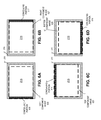
- FIGS. 5A-5C illustrate two displays being shifted on a vibration axis and displaying images associated with positions on the vibration axis to form a perceived image that disguises bezel seams of the two display, in accordance with an embodiment of the disclosure.
- FIG. 5A shows a cross-sectional top view of two display panels 500 , each including pixel region 515 surrounded by bezel 210 . When the display panels are at center position 531 , pixel regions 515 emit image light in viewing regions 543 - 545 , and 548 - 550 .
- Center position 531 may be the position the display panels 500 are in when vibration mechanisms 315 or 415 are not actuated or not being driven, although display panels 500 may be in a different position (other than center position 531 ) when the vibration mechanisms 315 or 415 are not being driven (turned off).
- Display panels 500 A and 500 B may both be shifted to the left to a first shift position 532 at a first time.
- pixel region 515 A may display a component image 511 .
- Component image 511 displays image light in viewing region 542 (as well as 543 and 544 ), where bezel 210 was previously positioned.
- pixel region 515 B may display a component image 521 .
- Component image 521 displays image light in viewing region 547 , where bezel 210 was previously positioned.
- Display panels 500 may both be shifted to the right to a second shift position 533 at a second time.
- pixel region 515 A may display a component image 512 .
- Component image 512 displays image light in viewing region 546 , where bezel 210 was previously positioned.
- pixel region 515 B may display a component image 522 .
- Component image 522 displays image light in viewing region 551 , where bezel 210 was previously positioned.
- the lateral translation from first shift position 532 to second shift position 533 may be twice bezel width 563 .
- Image light from component image 511 (viewing regions 542 - 544 ) and component image 512 (viewing region 544 - 546 ) may form compound image 515 (viewing region 542 - 546 ).
- Image light from component image 521 (viewing regions 547 - 549 ) and component image 522 (viewing regions 549 - 551 ) may form compound image 525 .
- Compound images 515 and 525 form perceived image 560 .
- Perceived image 560 spans from viewing region 542 - 551 .
- Perceived image 560 may be an integral image that includes image light from component images 511 , 512 , 521 , and 522 .
- pixel regions 515 A and 515 B emit image light in viewing regions 542 - 551 , a viewer may not perceive a seam created by bezels 210 , if the display panels 500 A and 500 B are vibrated at a fast enough frequency.
- the vibration frequency is 120 Hz. It is appreciated that each display panel in a multi-panel may have different vibration frequencies and the vibration frequencies may not be synchronized, in the embodiments illustrated in FIGS. 4A and 4B where the display panels are offset in the z dimension to prevent physical interference.
- FIG. 5B is a top view of display panels 500 A and 500 B and FIG. 5C is a corresponding front view of display panels 500 A and 500 B, as a viewer would see.
- pixel regions 515 A and 515 B display image light in viewing regions 542 , 543 , 545 - 548 , 550 , and 551 at either first shift position 532 and second shift position 533 .
- pixel regions 515 A and 515 B display image light in viewing regions 544 and viewing regions 549 in both first shift position 532 and second shift position 533 , which may contribute to viewing regions 544 and 549 having brighter image light in perceived image 560 .
- Pixel brightness of pixels in pixel regions 515 A and 515 B may be adjusted to compensate for uneven brightness in sections of compound images 515 and 525 . If viewing regions 544 and 549 have brighter image light, common image sections 574 and 579 of compound images 515 and 525 have brighter image light. Optionally, the light output of compound images 515 and 525 may be normalized so that image light brightness in the compound images is more even. If display panels 500 A and 500 B are organic light-emitting-diode (“OLED”) displays, OLED pixels in the display may be selectably driven to create the desired image brightness across compound images 515 and 525 .
- OLED organic light-emitting-diode
- component image 511 includes first end section 572 (corresponding to viewing regions 542 - 543 ) and common image section 574 (corresponding to viewing region 544 ). OLED pixels in pixel region 515 A that generate first end section 572 of component image 511 may be driven to be brighter than the pixels that generate common image section 574 of component image 511 , in order to even image brightness in compound image 515 .
- component image 512 includes second end section 576 (corresponding to viewing regions 545 - 546 ) and common image section 574 .
- OLED pixels in pixel region 515 A that generate second end section 576 of component image 512 may be driven to be brighter than the OLED pixels that generate common image section 574 of component image 512 , in order to even image brightness in compound image 515 .
- component image 521 includes first end section 577 (corresponding to viewing regions 547 - 548 ) and common image section 579 (corresponding to viewing region 549 ). OLED pixels in pixel region 515 B that generate first end section 577 may be driven to be brighter than pixels that generate common image section 579 of component image 521 , in order to even image brightness in compound image 525 .
- component image 522 includes second end section 587 (corresponding to viewing regions 550 - 551 ) and common image section 579 .
- OLED pixels in pixel region 515 B that generate second end section 5781 of component image 521 may be driven to be brighter than the OLED pixels that generate common image section 574 of component image 522 , in order to even image brightness in compound image 525 .
- the OLED pixels generating image light for common image sections 574 and 579 may be driven to emit less light to even out image brightness in compound images 515 and 525 .
- these techniques for evening image light in compound images that are described in connection with FIGS. 5A-5C could be applied to a multi-panel display with more than one vibration axis.
- the embodiment shown in FIG. 5A is only one example of creating a perceived image 560 that disguises or conceals bezel seams.
- more than two images are displayed to generate a compound image.
- four images are generated corresponding with four positions along a vibration axis (e.g. vibration axis 233 ) to generate a compound image or images.
- the display panel may need to be capable of an increased refresh rate when more images are displayed corresponding with positions along a vibration axis. It is appreciated that any number of images could be generated corresponding with different positions of the display panel. It is also appreciated that images could be generated with corresponding images along vibration axes that would be perceived as motion-picture media.
- a randomized pixel pattern is displayed in the end sections.
- Pixel randomization operates to reduce regular patterns (e.g. the straight edge of bezel 210 ) which the eye tends to easily identify, with irregular patterns.
- regular patterns e.g. the straight edge of bezel 210
- light from a randomized pixel pattern may be effective in disguising a bezel seam from a viewer when compared with viewing a stationary bezel.
- FIGS. 6A-6D illustrate an example display panel being shifted to disguise portions of different sides of a bezel, in accordance with an embodiment of the disclosure.
- FIGS. 6A-6B show how an example display panel could be shifted to disguise or conceal display panel bezels from side to side.
- pixel region 215 is shifted to the left (with the rest of display panel 200 ) to display left component image 626 .
- Pixels in concealing portion 616 of pixel region 215 display image light to disguise or conceal where bezel 210 was previously positioned.
- FIG. 6B pixel region 215 is shifted to the right to display right component image 627 .
- Pixels in concealing portion 617 of pixel region 215 display image light to disguise or conceal where bezel 210 was previously positioned.
- Left component image 626 and right component image 627 may combine to form a compound image that is part of an overall perceived image(s).
- FIGS. 6C-6D show how an example display panel would be shifted to disguise or conceal display panel bezels from top to bottom.
- pixel region 215 is shifted up to display top component image 628 .
- Pixels in concealing portion 618 of pixel region 215 display image light to disguise or conceal where bezel 210 was previously positioned.
- pixel region 215 is shifted down to display bottom component image 629 .
- Pixels in concealing portion 619 of pixel region 215 display image light to disguise or conceal where bezel 210 was previously positioned.
- Top component image 628 and bottom component image 629 may combine to form a compound image that is part of an overall perceived image(s).
- FIGS. 6A-6D may not adequately disguise or conceal the corners of the bezels of the display panels where the display panels intersect in the middle of the 2 ⁇ 2 matrix. This is because pixel region 215 in FIGS. 6A-6D does not shift to cover the far corners of the bezel 210 . Therefore, it may be advantageous to shift pixel region 215 to display image light where the corner of the bezel was previously positioned. Referring back to FIG. 2C , shifting pixel region 215 to the corners of the bezel could be achieved by shifting pixel region 215 on both of the axes in dual vibration axis 234 .
- vibration mechanism 315 / 415 may be configured as shown in FIG. 2D , where the two axes in diagonal dual vibration axis 235 run diagonally between the corners of the display panels. This may be advantageous in comparison to FIG. 2C because vibration mechanism 315 / 415 may only need to be driven to shift a display panel on one axis so that pixel region 215 can reach the locations shown in FIG. 7A-7D .
- FIGS. 7A-7D illustrate an example display panel being shifted to four different positions on two axes to display images that disguise portions of a bezel, in accordance with an embodiment of the disclosure.
- pixel region 215 is shifted up and to the left (with the rest of display panel 200 ) to display Northwest (“NW”) position image 726 .
- Pixels in concealing portion 716 of pixel region 215 display image light to disguise or conceal where portions of the top side and left side of bezel 210 were previously positioned.
- FIG. 7B pixel region 215 is shifted up and to the right to display Northeast (“NE”) position image 727 .
- NE Northeast
- Pixels in concealing portion 717 of pixel region 215 display image light to disguise or conceal where portions of the top side and right side of bezel 210 were previously positioned.
- pixel region 215 is shifted down and to the left to display Southwest (“SW”) position image 728 .
- Pixels in concealing portion 718 of pixel region 215 display image light to disguise or conceal where portions of the bottom side and left side of bezel 210 were previously positioned.
- FIG. 7D pixel region 215 is shifted down and to the right to display Southeast (“SE”) position image 729 .
- Pixels in concealing portion 719 of pixel region 215 display image light to disguise or conceal where portions of the bottom side and right side of bezel 210 were previously positioned.
- NW position image 726 , NE position image 727 , SW position image 728 , and SE position image 729 may be component images that combine to form a compound image that is part of an overall perceived image(s).
- FIG. 8 illustrates a flow chart illustrating an example process 800 of disguising seams in multi-panel displays, in accordance with an embodiment of the disclosure.
- the order in which some or all of the process blocks appear in process 800 should not be deemed limiting. Rather, one of ordinary skill in the art having the benefit of the present disclosure will understand that some of the process blocks may be executed in a variety of orders not illustrated, or even in parallel.
- display panels are shifted in first directions (e.g. to the left along a vibration axis) to first positions (e.g. first shift position 532 ), where first sides of bezels (e.g. FIG. 6 A's left side of bezel 210 or FIG. 7 A's left and top sides of bezel 210 ) were previously positioned.
- Pixel regions of the display panels e.g. pixel regions 515 A and 515 B
- first component-images e.g. component-images 511 and 521
- the display panels are shifted in second directions (e.g. right along a vibration axis) to second positions (e.g.
- second shift position 533 where second sides of bezels (e.g. FIG. 6 B's right side of bezel 210 or FIG. 7 B's right and bottom side of bezel 210 ) were previously positioned. Pixel regions of the display panels may then display second component-images (e.g. component images 512 and 522 ), in process block 820 . It is appreciated that all the display panels in a multi-panel display may not be shifted to their first position at the same time (synchronously) as the other display panels. In some embodiments, each display panel is shifted to its first position (via vibration mechanism 315 , for example) independently, or asynchronously, even if a vibration frequency of all the vibration mechanisms in the multi-panel display are vibrated at the same numerical frequency.
- vibration mechanism 315 for example
- a tangible non-transitory machine-readable storage medium includes any mechanism that provides (i.e., stores) information in a form accessible by a machine (e.g., a computer, network device, personal digital assistant, manufacturing tool, any device with a set of one or more processors, etc.).
- a machine-readable storage medium includes recordable/non-recordable media (e.g., read only memory (ROM), random access memory (RAM), magnetic disk storage media, optical storage media, flash memory devices, etc.).
Abstract
Description
Claims (20)
Priority Applications (1)
| Application Number | Priority Date | Filing Date | Title |
|---|---|---|---|
| US13/732,611 US9117383B1 (en) | 2012-04-20 | 2013-01-02 | Vibrating display panels for disguising seams in multi-panel displays |
Applications Claiming Priority (2)
| Application Number | Priority Date | Filing Date | Title |
|---|---|---|---|
| US201261636458P | 2012-04-20 | 2012-04-20 | |
| US13/732,611 US9117383B1 (en) | 2012-04-20 | 2013-01-02 | Vibrating display panels for disguising seams in multi-panel displays |
Publications (1)
| Publication Number | Publication Date |
|---|---|
| US9117383B1 true US9117383B1 (en) | 2015-08-25 |
Family
ID=49379814
Family Applications (8)
| Application Number | Title | Priority Date | Filing Date |
|---|---|---|---|
| US13/599,444 Active 2033-05-07 US9025111B2 (en) | 2012-04-20 | 2012-08-30 | Seamless display panel using fiber optic carpet |
| US13/657,667 Abandoned US20170206830A1 (en) | 2012-04-20 | 2012-10-22 | System and method of generating images from backside of photoactive layer |
| US13/657,691 Active 2034-02-07 US9646562B1 (en) | 2012-04-20 | 2012-10-22 | System and method of generating images on photoactive surfaces |
| US13/732,654 Abandoned US20150194123A1 (en) | 2012-04-20 | 2013-01-02 | Interconnecting display tiles for multi-panel displays |
| US13/732,611 Active 2033-06-01 US9117383B1 (en) | 2012-04-20 | 2013-01-02 | Vibrating display panels for disguising seams in multi-panel displays |
| US13/754,743 Active 2033-11-15 US9146400B1 (en) | 2012-04-20 | 2013-01-30 | Display panel tiling using seam-concealing optics |
| US13/754,750 Active 2033-07-18 US9053648B1 (en) | 2012-04-20 | 2013-01-30 | Tiled displays using multiple display panels over monolithic backlight modules |
| US13/754,732 Abandoned US20130279012A1 (en) | 2012-04-20 | 2013-01-30 | Seamless display panel tiling using an optical expansion layer |
Family Applications Before (4)
| Application Number | Title | Priority Date | Filing Date |
|---|---|---|---|
| US13/599,444 Active 2033-05-07 US9025111B2 (en) | 2012-04-20 | 2012-08-30 | Seamless display panel using fiber optic carpet |
| US13/657,667 Abandoned US20170206830A1 (en) | 2012-04-20 | 2012-10-22 | System and method of generating images from backside of photoactive layer |
| US13/657,691 Active 2034-02-07 US9646562B1 (en) | 2012-04-20 | 2012-10-22 | System and method of generating images on photoactive surfaces |
| US13/732,654 Abandoned US20150194123A1 (en) | 2012-04-20 | 2013-01-02 | Interconnecting display tiles for multi-panel displays |
Family Applications After (3)
| Application Number | Title | Priority Date | Filing Date |
|---|---|---|---|
| US13/754,743 Active 2033-11-15 US9146400B1 (en) | 2012-04-20 | 2013-01-30 | Display panel tiling using seam-concealing optics |
| US13/754,750 Active 2033-07-18 US9053648B1 (en) | 2012-04-20 | 2013-01-30 | Tiled displays using multiple display panels over monolithic backlight modules |
| US13/754,732 Abandoned US20130279012A1 (en) | 2012-04-20 | 2013-01-30 | Seamless display panel tiling using an optical expansion layer |
Country Status (4)
| Country | Link |
|---|---|
| US (8) | US9025111B2 (en) |
| CN (1) | CN104221071A (en) |
| TW (2) | TWI492199B (en) |
| WO (2) | WO2013158244A2 (en) |
Families Citing this family (76)
| Publication number | Priority date | Publication date | Assignee | Title |
|---|---|---|---|---|
| US9435939B2 (en) * | 2012-08-02 | 2016-09-06 | Apple Inc. | Displays with coherent fiber bundles |
| JP2015228536A (en) * | 2012-09-25 | 2015-12-17 | シャープ株式会社 | Display device and display method |
| US9274369B1 (en) * | 2012-10-30 | 2016-03-01 | Google Inc. | Seamless display with tapered fused fiber bundle overlay |
| US9123266B2 (en) * | 2013-11-19 | 2015-09-01 | Google Inc. | Seamless tileable display with peripheral magnification |
| CN104658436B (en) * | 2013-11-25 | 2018-09-28 | 丁炜慷 | A method of the point-to-point display input video on mosaic display screen |
| US9803833B2 (en) * | 2013-12-03 | 2017-10-31 | X Development Llc | Multi-aperture illumination layer for tileable display |
| US9349160B1 (en) | 2013-12-20 | 2016-05-24 | Google Inc. | Method, apparatus and system for enhancing a display of video data |
| KR102198783B1 (en) * | 2014-04-11 | 2021-01-05 | 삼성전자주식회사 | Method for displaying image using a plurality of display apparatus and Electronic apparatus thereof |
| CN105405360B (en) * | 2014-09-03 | 2018-03-20 | 深圳富泰宏精密工业有限公司 | Seamless spliced display device |
| US9529563B2 (en) * | 2014-09-30 | 2016-12-27 | X Development Llc | Masking mechanical separations between tiled display panels |
| US20160103263A1 (en) * | 2014-10-13 | 2016-04-14 | Google Inc. | Light transmission device with integration structures |
| CN104464536A (en) * | 2014-12-11 | 2015-03-25 | 广东威创视讯科技股份有限公司 | Display device |
| US10317687B2 (en) * | 2014-12-16 | 2019-06-11 | Samsung Electronics Co., Ltd. | Light path adjuster and display device including the same |
| CN105759432B (en) * | 2014-12-16 | 2019-08-09 | 北京三星通信技术研究有限公司 | Naked eye three-dimensional image display |
| US9557954B2 (en) * | 2014-12-23 | 2017-01-31 | X Development Llc | Display panel using direct emission pixel arrays |
| TWI570445B (en) * | 2015-02-06 | 2017-02-11 | 佳世達科技股份有限公司 | Display device with enlarged visible region |
| CN107405499A (en) * | 2015-02-26 | 2017-11-28 | 夏普株式会社 | Light irradiation substrate and light irradiation device |
| US10463875B2 (en) * | 2015-02-26 | 2019-11-05 | Sharp Kabushiki Kaisha | Light irradiation substrate |
| CN106297572A (en) * | 2015-05-29 | 2017-01-04 | 鸿富锦精密工业(深圳)有限公司 | Frame-free displaying device |
| US11143794B2 (en) | 2015-07-08 | 2021-10-12 | Shine Optoelectronics (Kunshan) Co., Ltd | Optical film |
| CN106338786B (en) * | 2015-07-08 | 2018-08-24 | 昇印光电(昆山)股份有限公司 | A kind of micro-optics imaging film |
| TWI557699B (en) * | 2015-08-06 | 2016-11-11 | 友達光電股份有限公司 | Display device |
| CN105206487B (en) * | 2015-10-08 | 2017-12-19 | 清华大学 | A kind of liquid metal plasma color display device and preparation method |
| KR102507472B1 (en) * | 2016-02-26 | 2023-03-09 | 삼성전자주식회사 | Antenna in Electronic Device with Display |
| US10310645B2 (en) * | 2016-03-15 | 2019-06-04 | Microsoft Technology Licensing, Llc | Display window with light steering |
| KR102517336B1 (en) | 2016-03-29 | 2023-04-04 | 삼성전자주식회사 | Display panel and multi-vision apparatus |
| CN105842907B (en) * | 2016-05-31 | 2022-07-01 | 京东方科技集团股份有限公司 | Display device and driving method thereof |
| ITUA20164519A1 (en) * | 2016-06-20 | 2017-12-20 | Fondazione St Italiano Tecnologia | VISUALIZER INCLUDING A PLURALITY OF LIGHT SOURCES AND A PLURALITY OF WAVE GUIDES |
| US10146090B2 (en) | 2016-08-01 | 2018-12-04 | Microsoft Technology Licensing, Llc | Minimizing border of a display device |
| US10126489B2 (en) | 2016-08-09 | 2018-11-13 | Microsoft Technology Licensing, Llc | Liquid crystal display module |
| KR102208872B1 (en) * | 2016-08-26 | 2021-01-28 | 삼성전자주식회사 | Display apparatus and driving method thereof |
| CN106199974A (en) * | 2016-09-28 | 2016-12-07 | 京东方科技集团股份有限公司 | A kind of nearly eye display device |
| US20180108330A1 (en) * | 2016-10-18 | 2018-04-19 | Lenovo (Singapore) Pte. Ltd. | Electronic device with flexible display having multiple viewing regions |
| US10223952B2 (en) * | 2016-10-26 | 2019-03-05 | Microsoft Technology Licensing, Llc | Curved edge display with controlled distortion |
| US10185064B2 (en) | 2016-10-26 | 2019-01-22 | Microsoft Technology Licensing, Llc | Curved edge display with controlled luminance |
| US10628111B2 (en) * | 2016-11-08 | 2020-04-21 | Frank Michael Weyer | Method and apparatus for optically concealing video wall seams |
| KR20180051976A (en) * | 2016-11-09 | 2018-05-17 | 엘지전자 주식회사 | Display apparatus |
| WO2018139996A1 (en) * | 2017-01-25 | 2018-08-02 | Hewlett-Packard Development Company, L.P. | Curved modular display |
| CN108630111A (en) * | 2017-03-17 | 2018-10-09 | 诚屏科技股份有限公司 | Display device and display equipment |
| US10716223B2 (en) | 2017-04-17 | 2020-07-14 | Google Llc | Frame assembly for an electronic device display |
| US20180301484A1 (en) * | 2017-04-17 | 2018-10-18 | Semiconductor Components Industries, Llc | Image sensors with high dynamic range and autofocusing hexagonal pixels |
| WO2018211603A1 (en) * | 2017-05-16 | 2018-11-22 | オリンパス株式会社 | Image capture device |
| RU2648563C1 (en) * | 2017-07-03 | 2018-03-26 | Алексей Викторович Шторм | Method for determining the position of video modules within the group |
| RU177479U1 (en) * | 2017-07-07 | 2018-02-26 | Анастасия Сергеевна Чепрасова | MULTI-LAYERED VOLUME ADVERTISING LED MODULE |
| CN110914751B (en) | 2017-07-11 | 2023-12-26 | 康宁股份有限公司 | Tiled display and method of manufacturing the same |
| US11296176B2 (en) | 2017-07-27 | 2022-04-05 | Semiconductor Energy Laboratory Co., Ltd. | Display panel, display device, input/output device, and data processing device |
| US10636352B2 (en) * | 2017-08-25 | 2020-04-28 | Wuhan China Star Optoelectronics Semiconductor Display Technology Co., Ltd. | Display panel of active matrix organic light emitting diode, and display device |
| CN109521976B (en) * | 2017-09-19 | 2020-08-07 | 京东方科技集团股份有限公司 | Display panel frame, display terminal, splicing display device and control method |
| KR102407475B1 (en) * | 2017-12-08 | 2022-06-13 | 삼성전자주식회사 | Display apparatus and controlling method thereof |
| WO2019145782A2 (en) | 2018-01-23 | 2019-08-01 | Clear and Dark Ltd. | Systems, methods, and apparatus for forming optical articles, and optical articles formed by the same |
| US10838250B2 (en) * | 2018-02-07 | 2020-11-17 | Lockheed Martin Corporation | Display assemblies with electronically emulated transparency |
| CN108335636B (en) * | 2018-03-19 | 2023-12-08 | 蒋翔东 | Optical frameless spliced display device |
| TWI676064B (en) * | 2018-03-29 | 2019-11-01 | 友達光電股份有限公司 | Display device |
| TWI669816B (en) * | 2018-04-18 | 2019-08-21 | 友達光電股份有限公司 | Tiling display panel and manufacturing method thereof |
| WO2019240986A1 (en) * | 2018-06-12 | 2019-12-19 | Corning Incorporated | Display tile support structure |
| CN111028697A (en) * | 2018-10-09 | 2020-04-17 | 财团法人工业技术研究院 | Tiled display device |
| US11810484B2 (en) | 2018-10-09 | 2023-11-07 | Industrial Technology Research Institute | Spliced display |
| CN109448564B (en) * | 2019-01-04 | 2021-01-29 | 京东方科技集团股份有限公司 | Display panel, manufacturing method thereof and display device |
| CN110010025A (en) * | 2019-03-31 | 2019-07-12 | 湖南凯星电子科技有限公司 | A kind of constructive method of module lamp box |
| CN110047407A (en) * | 2019-04-01 | 2019-07-23 | 方迪勇 | A kind of constructive method of assembling-type modular lamp box |
| TWI682530B (en) * | 2019-05-29 | 2020-01-11 | 友達光電股份有限公司 | Light emitting diode panel and tiling display apparatus |
| KR20210019895A (en) | 2019-08-13 | 2021-02-23 | 삼성전자주식회사 | Electronic apparatus and controlling method thereof |
| US11513554B1 (en) | 2019-08-23 | 2022-11-29 | Apple Inc. | Electronic devices having displays with borders of image transport material |
| US11774644B1 (en) | 2019-08-29 | 2023-10-03 | Apple Inc. | Electronic devices with image transport layers having light absorbing material |
| KR20210049383A (en) * | 2019-10-25 | 2021-05-06 | 삼성전자주식회사 | Display apparatus and control method thereof |
| CN112863326B (en) * | 2019-11-12 | 2022-12-09 | Oppo广东移动通信有限公司 | Transparent screen, manufacturing method of transparent screen and mobile terminal |
| CN111048000A (en) * | 2019-12-26 | 2020-04-21 | 深圳市华星光电半导体显示技术有限公司 | Splicing display panel and splicing display device |
| CN111290154A (en) * | 2020-02-24 | 2020-06-16 | 京东方科技集团股份有限公司 | Display device and spliced screen |
| CN111192526B (en) * | 2020-03-18 | 2022-02-22 | 深圳市华星光电半导体显示技术有限公司 | Display device and tiled display device |
| CN114008700B (en) * | 2020-05-28 | 2023-10-24 | 京东方科技集团股份有限公司 | Display device and method for manufacturing the same |
| US11573450B1 (en) * | 2020-09-23 | 2023-02-07 | Apple Inc. | Electronic devices with chemically strengthened coherent fiber bundles |
| WO2022085824A1 (en) * | 2020-10-22 | 2022-04-28 | 엘지전자 주식회사 | Cover glass, method for manufacturing cover glass, and mobile terminal |
| JP2022104258A (en) * | 2020-12-28 | 2022-07-08 | 三菱電機株式会社 | Display unit, display device, and manufacturing method of display unit |
| CN112770098B (en) * | 2020-12-31 | 2023-05-30 | Oppo广东移动通信有限公司 | Color temperature detection assembly, image processing terminal, method and device |
| US11778858B1 (en) | 2021-01-04 | 2023-10-03 | Apple Inc. | Electronic device displays having microlenses |
| KR20220100759A (en) * | 2021-01-08 | 2022-07-18 | 삼성디스플레이 주식회사 | Tiled display device having a plurality of display panels |
Citations (11)
| Publication number | Priority date | Publication date | Assignee | Title |
|---|---|---|---|---|
| US20020167459A1 (en) * | 2001-05-11 | 2002-11-14 | Xerox Corporation | Methods of using mixed resolution displays |
| US20040001166A1 (en) | 2002-04-17 | 2004-01-01 | Shigeaki Nimura | Optical path deflecting element, optical path deflecting apparatus, image displaying apparatus, optical element and manufacturing method thereof |
| US20040208394A1 (en) * | 2003-04-16 | 2004-10-21 | Sony Corporation | Image display device and method for preventing image Blurring |
| US20050052376A1 (en) * | 2003-08-19 | 2005-03-10 | Shivji Shiraz M. | Method and apparatus for light emitting devices based display |
| US20060114172A1 (en) * | 2004-11-26 | 2006-06-01 | Giotti, Inc. | Method and apparatus for LED based modular display |
| US7145611B2 (en) | 2000-12-22 | 2006-12-05 | Honeywell International, Inc. | Seamless tiled display system |
| US20060279702A1 (en) | 2005-06-09 | 2006-12-14 | Kettle Wiatt E | Projection assembly |
| US20070097323A1 (en) | 2005-10-31 | 2007-05-03 | Charles Otis | Electro-optical wobulator |
| US20080143969A1 (en) | 2006-12-15 | 2008-06-19 | Richard Aufranc | Dynamic superposition system and method for multi-projection display |
| US20090079681A1 (en) * | 2004-06-30 | 2009-03-26 | Youn Gyoung Chang | Liquid crystal display device and luminance difference compensating method thereof |
| US7688506B2 (en) | 2006-01-25 | 2010-03-30 | Sony Corporation | Screen and image projection apparatus |
Family Cites Families (119)
| Publication number | Priority date | Publication date | Assignee | Title |
|---|---|---|---|---|
| US3357770A (en) * | 1961-10-02 | 1967-12-12 | Intermountain Res And Engineer | Stereoscopic viewing apparatus which includes a curved lenticular screen in front ofa curved picture supporting surface |
| JPS5464494A (en) * | 1977-10-31 | 1979-05-24 | Sharp Corp | Liquid crystal display unit |
| DE69032645T2 (en) | 1990-04-02 | 1999-04-08 | Koninkl Philips Electronics Nv | Data processing system with input data based on gestures |
| JPH06102509A (en) * | 1992-06-17 | 1994-04-15 | Xerox Corp | Full-color display device having optical coupling lens array |
| JP3133228B2 (en) | 1995-03-31 | 2001-02-05 | シャープ株式会社 | Display device |
| JP3079969B2 (en) * | 1995-09-14 | 2000-08-21 | 日本電気株式会社 | Complete contact image sensor and method of manufacturing the same |
| JPH09159985A (en) * | 1995-12-08 | 1997-06-20 | Mitsubishi Electric Corp | Picture display system |
| US6124974A (en) * | 1996-01-26 | 2000-09-26 | Proxemics | Lenslet array systems and methods |
| US5661531A (en) | 1996-01-29 | 1997-08-26 | Rainbow Displays Inc. | Tiled, flat-panel display having invisible seams |
| US5867236A (en) | 1996-05-21 | 1999-02-02 | Rainbow Displays, Inc. | Construction and sealing of tiled, flat-panel displays |
| GB9618720D0 (en) * | 1996-09-07 | 1996-10-16 | Philips Electronics Nv | Electrical device comprising an array of pixels |
| US5719395A (en) | 1996-09-12 | 1998-02-17 | Stress Photonics Inc. | Coating tolerant thermography |
| JP4013286B2 (en) * | 1997-01-22 | 2007-11-28 | 松下電器産業株式会社 | Image encoding device and image decoding device |
| JP3968477B2 (en) | 1997-07-07 | 2007-08-29 | ソニー株式会社 | Information input device and information input method |
| US6072494A (en) | 1997-10-15 | 2000-06-06 | Electric Planet, Inc. | Method and apparatus for real-time gesture recognition |
| JPH11126029A (en) * | 1997-10-22 | 1999-05-11 | Yazaki Corp | Display unit |
| US8479122B2 (en) | 2004-07-30 | 2013-07-02 | Apple Inc. | Gestures for touch sensitive input devices |
| GB9809731D0 (en) * | 1998-05-08 | 1998-07-08 | Koninkl Philips Electronics Nv | CRT Display systems |
| JP3730436B2 (en) * | 1999-03-30 | 2006-01-05 | 株式会社ニデック | Corneal shape inspection device |
| JP4912520B2 (en) | 1999-05-31 | 2012-04-11 | 三星モバイルディスプレイ株式會社 | Multi display device |
| GB9916286D0 (en) * | 1999-07-12 | 1999-09-15 | Koninkl Philips Electronics Nv | Display systems using flat matrix display panels |
| US6195016B1 (en) * | 1999-08-27 | 2001-02-27 | Advance Display Technologies, Inc. | Fiber optic display system with enhanced light efficiency |
| US6495833B1 (en) | 2000-01-20 | 2002-12-17 | Research Foundation Of Cuny | Sub-surface imaging under paints and coatings using early light spectroscopy |
| JP3983953B2 (en) * | 2000-03-10 | 2007-09-26 | パイオニア株式会社 | Stereoscopic two-dimensional image display apparatus and image display method |
| CA2403094C (en) * | 2000-03-17 | 2011-07-12 | Zograph, Llc | High acuity lens system |
| AU2000254964A1 (en) | 2000-06-16 | 2002-01-08 | Gl Displays, Inc. | Seamless tiled active matrix liquid crystal display |
| GB0028890D0 (en) | 2000-11-27 | 2001-01-10 | Isis Innovation | Visual display screen arrangement |
| JP2002214405A (en) * | 2001-01-22 | 2002-07-31 | Omron Corp | Lens array substrate and image display device |
| JP2002250895A (en) * | 2001-02-23 | 2002-09-06 | Mixed Reality Systems Laboratory Inc | Stereoscopic image display method and stereoscopic image display device using the same |
| GB0107076D0 (en) * | 2001-03-21 | 2001-05-09 | Screen Technology Ltd | Liquid-crystal display using emissive elements |
| EP1666964B1 (en) * | 2001-04-02 | 2018-12-19 | E Ink Corporation | Electrophoretic medium with improved image stability |
| US7259747B2 (en) | 2001-06-05 | 2007-08-21 | Reactrix Systems, Inc. | Interactive video display system |
| GB2377110A (en) * | 2001-06-30 | 2002-12-31 | Hewlett Packard Co | Movable image projection from portable data storage media |
| US6937742B2 (en) | 2001-09-28 | 2005-08-30 | Bellsouth Intellectual Property Corporation | Gesture activated home appliance |
| US6822389B2 (en) | 2001-10-11 | 2004-11-23 | Intel Corporation | Array display including resilient material in the seam |
| GB0210568D0 (en) * | 2002-05-08 | 2002-06-19 | Screen Technology Ltd | Display |
| US6881946B2 (en) | 2002-06-19 | 2005-04-19 | Eastman Kodak Company | Tiled electro-optic imaging device |
| JP3969252B2 (en) * | 2002-08-27 | 2007-09-05 | 日本電気株式会社 | Stereoscopic image plane image switching display device and portable terminal device |
| JP4230187B2 (en) * | 2002-09-25 | 2009-02-25 | シャープ株式会社 | Microlens array manufacturing method and microlens array manufacturing apparatus |
| GB0223883D0 (en) | 2002-10-15 | 2002-11-20 | Seamless Display Ltd | Visual display screen arrangement |
| US7186004B2 (en) * | 2002-12-31 | 2007-03-06 | Karlton David Powell | Homogenizing optical sheet, method of manufacture, and illumination system |
| US6840627B2 (en) | 2003-01-21 | 2005-01-11 | Hewlett-Packard Development Company, L.P. | Interactive display device |
| US7070278B2 (en) * | 2003-01-29 | 2006-07-04 | Mems Optical, Inc. | Autostereoscopic 3-D display |
| JP3970784B2 (en) * | 2003-02-10 | 2007-09-05 | シャープ株式会社 | Microlens substrate, liquid crystal display element including the same, and projection type liquid crystal display device |
| JP2004251981A (en) * | 2003-02-18 | 2004-09-09 | Seiko Epson Corp | Combined display device |
| US20040205394A1 (en) | 2003-03-17 | 2004-10-14 | Plutowski Mark Earl | Method and apparatus to implement an errands engine |
| US7202602B2 (en) | 2003-04-08 | 2007-04-10 | Organic Lighting Technologies Llc | Metal seal packaging for organic light emitting diode device |
| US7071614B2 (en) | 2003-06-30 | 2006-07-04 | Organic Lighting Technologies Llc | Electron and hole modulating electrodes in organic light emitting diodes |
| US20060176269A1 (en) | 2003-07-24 | 2006-08-10 | Koninklijke Philips Electronics N.V. | Activation of electronic paint with registration codes |
| US7667815B2 (en) | 2003-08-27 | 2010-02-23 | Ming Su | Multi-panel monitor displaying systems |
| GB2405519A (en) * | 2003-08-30 | 2005-03-02 | Sharp Kk | A multiple-view directional display |
| CA2542793A1 (en) | 2003-11-03 | 2005-05-12 | Super-Imaging, Inc. | Light emitting material integrated into a substantially transparent substrate |
| US7155305B2 (en) | 2003-11-04 | 2006-12-26 | Universal Electronics Inc. | System and methods for home appliance identification and control in a networked environment |
| US6885010B1 (en) | 2003-11-12 | 2005-04-26 | Thermo Electron Corporation | Carbon nanotube electron ionization sources |
| US7205526B2 (en) * | 2003-12-22 | 2007-04-17 | Micron Technology, Inc. | Methods of fabricating layered lens structures |
| US8723779B2 (en) | 2004-01-26 | 2014-05-13 | Mcmaster University | Tiled optical fiber display |
| WO2005079376A2 (en) * | 2004-02-19 | 2005-09-01 | New York University | Method and apparatus for an autostereoscopic display having a lenticular lenslet array |
| SI21767A (en) | 2004-04-28 | 2005-10-31 | Iskra Mehanizmi, Industrija Mehanizmov, Aparatov In Sistemov D.D. | Illumination of the electromagnetic display panels |
| US7421647B2 (en) | 2004-07-09 | 2008-09-02 | Bruce Reiner | Gesture-based reporting method and system |
| US20060044215A1 (en) * | 2004-08-24 | 2006-03-02 | Brody Thomas P | Scalable tiled display assembly for forming a large-area flat-panel display by using modular display tiles |
| US7498743B2 (en) | 2004-12-14 | 2009-03-03 | Munisamy Anandan | Large area plasma display with increased discharge path |
| KR20060096228A (en) * | 2005-03-03 | 2006-09-11 | 삼성전자주식회사 | 2d and 3d image switching display system |
| US7474286B2 (en) * | 2005-04-01 | 2009-01-06 | Spudnik, Inc. | Laser displays using UV-excitable phosphors emitting visible colored light |
| US20060227147A1 (en) * | 2005-04-07 | 2006-10-12 | Toon Diels | Method and apparatus for an image presentation device with illumination control for black image processing |
| US20070001927A1 (en) * | 2005-07-01 | 2007-01-04 | Eastman Kodak Company | Tiled display for electronic signage |
| US8661540B2 (en) | 2005-10-07 | 2014-02-25 | Imation Corp. | Method and apparatus for secure credential entry without physical entry |
| US20070139367A1 (en) | 2005-12-21 | 2007-06-21 | Goffin Glen P | Apparatus and method for providing non-tactile text entry |
| US7509402B2 (en) | 2006-03-16 | 2009-03-24 | Exceptional Innovation, Llc | Automation control system having a configuration tool and two-way ethernet communication for web service messaging, discovery, description, and eventing that is controllable with a touch-screen display |
| WO2007114918A2 (en) * | 2006-04-04 | 2007-10-11 | Microvision, Inc. | Electronic display with photoluminescent wavelength conversion |
| US7768525B2 (en) | 2006-05-18 | 2010-08-03 | Microsoft Corporation | Dynamic paint pickup |
| KR20090013196A (en) * | 2006-05-24 | 2009-02-04 | 코닌클리케 필립스 일렉트로닉스 엔.브이. | Method and apparatus for auto-commissioning of led based display configurations |
| US7661068B2 (en) | 2006-06-12 | 2010-02-09 | Microsoft Corporation | Extended eraser functions |
| US20080004953A1 (en) | 2006-06-30 | 2008-01-03 | Microsoft Corporation | Public Display Network For Online Advertising |
| US7663312B2 (en) | 2006-07-24 | 2010-02-16 | Munisamy Anandan | Flexible OLED light source |
| DE102006043947A1 (en) * | 2006-09-14 | 2008-04-03 | Schott Ag | Display device with fiber optic arrangement |
| US8080926B2 (en) * | 2006-09-25 | 2011-12-20 | Samsung Electronics Co., Ltd. | Multi-display apparatus and method of manufacturing the same |
| US8243127B2 (en) * | 2006-10-27 | 2012-08-14 | Zecotek Display Systems Pte. Ltd. | Switchable optical imaging system and related 3D/2D image switchable apparatus |
| CN200990174Y (en) * | 2006-12-31 | 2007-12-12 | 杭州安瑞科技有限公司 | Slitless split large screen |
| US7611396B2 (en) | 2007-02-27 | 2009-11-03 | Disney Enterprises, Inc. | Illuminated balloon with an externally mounted, rear projector |
| JP2008309963A (en) | 2007-06-13 | 2008-12-25 | Hitachi Displays Ltd | Liquid crystal display device equipped with microlens array |
| US7905618B2 (en) * | 2007-07-19 | 2011-03-15 | Samsung Led Co., Ltd. | Backlight unit |
| US7934862B2 (en) | 2007-09-24 | 2011-05-03 | Munisamy Anandan | UV based color pixel backlight for liquid crystal display |
| JP2009098239A (en) | 2007-10-15 | 2009-05-07 | Idec Corp | Optical fiber image apparatus |
| WO2009066436A1 (en) * | 2007-11-22 | 2009-05-28 | Sharp Kabushiki Kaisha | Display device |
| KR101079598B1 (en) | 2007-12-18 | 2011-11-03 | 삼성전자주식회사 | Display apparatus and control method thereof |
| US8007110B2 (en) | 2007-12-28 | 2011-08-30 | Motorola Mobility, Inc. | Projector system employing depth perception to detect speaker position and gestures |
| US7729055B2 (en) * | 2008-03-20 | 2010-06-01 | Aptina Imaging Corporation | Method and apparatus providing concave microlenses for semiconductor imaging devices |
| EP2269123A4 (en) * | 2008-03-20 | 2016-09-07 | Cooper Technologies Co | Energy management system |
| US8692737B2 (en) * | 2008-06-25 | 2014-04-08 | Sharp Kabushiki Kaisha | Display device including light-transmitting cover with a lens portion |
| CN102067197A (en) | 2008-06-26 | 2011-05-18 | 夏普株式会社 | Display device and electronic device |
| US8863038B2 (en) | 2008-09-08 | 2014-10-14 | Qualcomm Incorporated | Multi-panel electronic device |
| US8933874B2 (en) | 2008-09-08 | 2015-01-13 | Patrik N. Lundqvist | Multi-panel electronic device |
| TWI387355B (en) * | 2008-09-09 | 2013-02-21 | Novatek Microelectronics Corp | Method and apparatus for color adjustment in a display device |
| US8591039B2 (en) * | 2008-10-28 | 2013-11-26 | Smart Technologies Ulc | Image projection methods and interactive input/projection systems employing the same |
| US7935963B2 (en) | 2008-11-18 | 2011-05-03 | Munisamy Anandan | Hybrid organic light emitting diode |
| US8884870B2 (en) | 2008-12-19 | 2014-11-11 | Immersion Corporation | Interactive painting game and associated controller |
| US20120050687A1 (en) | 2008-12-24 | 2012-03-01 | Elizabeth Berry | Creating a lighting effect |
| JP2010169976A (en) | 2009-01-23 | 2010-08-05 | Sony Corp | Spatial image display |
| JP4725654B2 (en) * | 2009-01-30 | 2011-07-13 | ソニー株式会社 | Lens array device and image display device |
| US20100284089A1 (en) * | 2009-05-07 | 2010-11-11 | San-Woei Shyu | Stacked optical glass lens array, stacked lens module and manufacturing method thereof |
| KR20110008486A (en) | 2009-07-20 | 2011-01-27 | 장윤석 | Lens plate, display device including lens plate, and fabrication of lens plate and display device |
| KR100954476B1 (en) | 2009-08-12 | 2010-04-22 | 도레이새한 주식회사 | Optical sheet for controlling the direction of ray of light |
| US8730183B2 (en) | 2009-09-03 | 2014-05-20 | Obscura Digital | Large scale multi-user, multi-touch system |
| US20110080665A1 (en) | 2009-10-05 | 2011-04-07 | Delphi Technologies, Inc. | Visual gap mitigation apparatus for a segmented display panel |
| US8589968B2 (en) | 2009-12-31 | 2013-11-19 | Motorola Mobility Llc | Systems and methods providing content on a display based upon facial recognition of a viewer |
| CN102741730A (en) * | 2010-02-10 | 2012-10-17 | 皇家飞利浦电子股份有限公司 | Lighting apparatus |
| WO2011112633A1 (en) | 2010-03-09 | 2011-09-15 | Flir Systems, Inc. | Imager with multiple sensor arrays |
| US8619367B2 (en) * | 2010-03-16 | 2013-12-31 | Olympus Corporation | Display apparatus, display unit, electronic equipment, mobile electronic equipment, mobile telephone, and image pickup apparatus |
| KR101173744B1 (en) * | 2010-04-05 | 2012-08-13 | 엘지이노텍 주식회사 | Polarization conversion apparatus |
| WO2012003233A1 (en) * | 2010-06-30 | 2012-01-05 | Thomas Zerega | Display with anti-moire optical system and method |
| US8682030B2 (en) * | 2010-09-24 | 2014-03-25 | Microsoft Corporation | Interactive display |
| JP5494415B2 (en) * | 2010-10-27 | 2014-05-14 | セイコーエプソン株式会社 | Projection type display device and control method thereof |
| US20120154511A1 (en) | 2010-12-20 | 2012-06-21 | Shi-Ping Hsu | Systems and methods for providing geographically distributed creative design |
| US8603723B2 (en) | 2011-01-26 | 2013-12-10 | Taiwan Textile Research Institute | Image transfer process |
| US20120218417A1 (en) | 2011-02-28 | 2012-08-30 | Ford Global Technologies, Llc | Short throw ratio fluorescent color video display device |
| TWI444088B (en) * | 2011-03-11 | 2014-07-01 | Nat Univ Tsing Hua | Color led display device without color separation |
| US9342610B2 (en) | 2011-08-25 | 2016-05-17 | Microsoft Technology Licensing, Llc | Portals: registered objects as virtualized, personalized displays |
| US9164596B1 (en) | 2012-10-22 | 2015-10-20 | Google Inc. | Method and apparatus for gesture interaction with a photo-active painted surface |
| US9014417B1 (en) | 2012-10-22 | 2015-04-21 | Google Inc. | Method and apparatus for themes using photo-active surface paint |
-
2012
- 2012-08-30 US US13/599,444 patent/US9025111B2/en active Active
- 2012-10-22 US US13/657,667 patent/US20170206830A1/en not_active Abandoned
- 2012-10-22 US US13/657,691 patent/US9646562B1/en active Active
-
2013
- 2013-01-02 US US13/732,654 patent/US20150194123A1/en not_active Abandoned
- 2013-01-02 US US13/732,611 patent/US9117383B1/en active Active
- 2013-01-30 US US13/754,743 patent/US9146400B1/en active Active
- 2013-01-30 US US13/754,750 patent/US9053648B1/en active Active
- 2013-01-30 US US13/754,732 patent/US20130279012A1/en not_active Abandoned
- 2013-03-08 WO PCT/US2013/030026 patent/WO2013158244A2/en active Application Filing
- 2013-03-11 CN CN201380019714.0A patent/CN104221071A/en active Pending
- 2013-03-11 WO PCT/US2013/030256 patent/WO2013158248A1/en active Application Filing
- 2013-03-28 TW TW102111248A patent/TWI492199B/en not_active IP Right Cessation
- 2013-03-28 TW TW102111247A patent/TWI474298B/en not_active IP Right Cessation
Patent Citations (11)
| Publication number | Priority date | Publication date | Assignee | Title |
|---|---|---|---|---|
| US7145611B2 (en) | 2000-12-22 | 2006-12-05 | Honeywell International, Inc. | Seamless tiled display system |
| US20020167459A1 (en) * | 2001-05-11 | 2002-11-14 | Xerox Corporation | Methods of using mixed resolution displays |
| US20040001166A1 (en) | 2002-04-17 | 2004-01-01 | Shigeaki Nimura | Optical path deflecting element, optical path deflecting apparatus, image displaying apparatus, optical element and manufacturing method thereof |
| US20040208394A1 (en) * | 2003-04-16 | 2004-10-21 | Sony Corporation | Image display device and method for preventing image Blurring |
| US20050052376A1 (en) * | 2003-08-19 | 2005-03-10 | Shivji Shiraz M. | Method and apparatus for light emitting devices based display |
| US20090079681A1 (en) * | 2004-06-30 | 2009-03-26 | Youn Gyoung Chang | Liquid crystal display device and luminance difference compensating method thereof |
| US20060114172A1 (en) * | 2004-11-26 | 2006-06-01 | Giotti, Inc. | Method and apparatus for LED based modular display |
| US20060279702A1 (en) | 2005-06-09 | 2006-12-14 | Kettle Wiatt E | Projection assembly |
| US20070097323A1 (en) | 2005-10-31 | 2007-05-03 | Charles Otis | Electro-optical wobulator |
| US7688506B2 (en) | 2006-01-25 | 2010-03-30 | Sony Corporation | Screen and image projection apparatus |
| US20080143969A1 (en) | 2006-12-15 | 2008-06-19 | Richard Aufranc | Dynamic superposition system and method for multi-projection display |
Also Published As
| Publication number | Publication date |
|---|---|
| US9053648B1 (en) | 2015-06-09 |
| US9646562B1 (en) | 2017-05-09 |
| US20130278872A1 (en) | 2013-10-24 |
| US9146400B1 (en) | 2015-09-29 |
| WO2013158244A3 (en) | 2014-03-13 |
| US20170206830A1 (en) | 2017-07-20 |
| WO2013158248A1 (en) | 2013-10-24 |
| CN104221071A (en) | 2014-12-17 |
| TWI492199B (en) | 2015-07-11 |
| TWI474298B (en) | 2015-02-21 |
| TW201346856A (en) | 2013-11-16 |
| WO2013158244A2 (en) | 2013-10-24 |
| US9025111B2 (en) | 2015-05-05 |
| US20150194123A1 (en) | 2015-07-09 |
| TW201346857A (en) | 2013-11-16 |
| US20130279012A1 (en) | 2013-10-24 |
Similar Documents
| Publication | Publication Date | Title |
|---|---|---|
| US9117383B1 (en) | Vibrating display panels for disguising seams in multi-panel displays | |
| TWI549117B (en) | Configurations for tileable display apparatus with multiple pixel arrays | |
| TWI576803B (en) | Masking mechanical separations between tiled display panels | |
| EP3306376B1 (en) | 2d/3d switchable display panel, and display method and display device therefor | |
| KR100679504B1 (en) | Spatial image type display | |
| EP3357058B1 (en) | Method and system for performing color filter offsets in order to reduce moiré interference in a display system including multiple displays | |
| JP4823571B2 (en) | 3D display device | |
| EP3368943B1 (en) | Method and system for performing panel vibration and selective backlight control to reduce moiré interference in a display system including multiple displays | |
| US20130093646A1 (en) | Electronic display tiling apparatus and propagation based method thereof | |
| US20150022727A1 (en) | Tileable display apparatus | |
| KR101157425B1 (en) | Large size display device of tiled method | |
| WO2017117928A1 (en) | Display module, display device, and drive method thereof | |
| JP3605572B2 (en) | Three-dimensional image display device, point light emitting member and point light transmitting member | |
| WO2015133488A1 (en) | Video display device | |
| JP6411257B2 (en) | Display device and control method thereof | |
| WO2017024742A1 (en) | 3d display panel, 3d display method and display device | |
| JP2007041218A (en) | Image display device | |
| JP2007139865A (en) | Three-dimensional image display device | |
| US9709816B2 (en) | Image display apparatus using transflective electro-optic device | |
| JP2006098775A (en) | Three-dimensional image display system | |
| KR102320630B1 (en) | Curved cover for curved display and curved type display appartus comprising the same | |
| WO2016117326A1 (en) | Display device | |
| US20120105497A1 (en) | Auto-stereoscopic 3d display and display method thereof | |
| JP2010271730A (en) | Method for driving display device | |
| JP2012242430A (en) | Display device |
Legal Events
| Date | Code | Title | Description |
|---|---|---|---|
| AS | Assignment |
Owner name: GOOGLE INC., CALIFORNIA Free format text: ASSIGNMENT OF ASSIGNORS INTEREST;ASSIGNORS:LEE, JOHNNY;TELLER, ERIC;SIGNING DATES FROM 20121204 TO 20121216;REEL/FRAME:029556/0547 |
|
| STCF | Information on status: patent grant |
Free format text: PATENTED CASE |
|
| AS | Assignment |
Owner name: X DEVELOPMENT LLC, CALIFORNIA Free format text: ASSIGNMENT OF ASSIGNORS INTEREST;ASSIGNOR:GOOGLE INC.;REEL/FRAME:039900/0610 Effective date: 20160901 |
|
| AS | Assignment |
Owner name: GOOGLE LLC, CALIFORNIA Free format text: CHANGE OF NAME;ASSIGNOR:GOOGLE INC.;REEL/FRAME:044144/0001 Effective date: 20170929 |
|
| AS | Assignment |
Owner name: GOOGLE LLC, CALIFORNIA Free format text: CORRECTIVE ASSIGNMENT TO CORRECT THE CORRECTIVE BY NULLIFICATION TO CORRECT INCORRECTLY RECORDED APPGE OF NAME;ASSIGNOR:GOOGLE INC.;REEL/FRAME:047894/0508 LICATION NUMBERS PREVIOUSLY RECORDED ON REEL 044144 FRAME 0001. ASSIGNOR(S) HEREBY CONFIRMS THE CHAN Effective date: 20170929 Owner name: GOOGLE LLC, CALIFORNIA Free format text: CORRECTIVE ASSIGNMENT TO CORRECT THE CORRECTIVE BY NULLIFICATION TO CORRECT INCORRECTLY RECORDED APPLICATION NUMBERS PREVIOUSLY RECORDED ON REEL 044144 FRAME 0001. ASSIGNOR(S) HEREBY CONFIRMS THE CHANGE OF NAME;ASSIGNOR:GOOGLE INC.;REEL/FRAME:047894/0508 Effective date: 20170929 |
|
| MAFP | Maintenance fee payment |
Free format text: PAYMENT OF MAINTENANCE FEE, 4TH YEAR, LARGE ENTITY (ORIGINAL EVENT CODE: M1551); ENTITY STATUS OF PATENT OWNER: LARGE ENTITY Year of fee payment: 4 |
|
| MAFP | Maintenance fee payment |
Free format text: PAYMENT OF MAINTENANCE FEE, 8TH YEAR, LARGE ENTITY (ORIGINAL EVENT CODE: M1552); ENTITY STATUS OF PATENT OWNER: LARGE ENTITY Year of fee payment: 8 |