JP2007139865A - Three-dimensional image display device - Google Patents
Three-dimensional image display device Download PDFInfo
- Publication number
- JP2007139865A JP2007139865A JP2005330048A JP2005330048A JP2007139865A JP 2007139865 A JP2007139865 A JP 2007139865A JP 2005330048 A JP2005330048 A JP 2005330048A JP 2005330048 A JP2005330048 A JP 2005330048A JP 2007139865 A JP2007139865 A JP 2007139865A
- Authority
- JP
- Japan
- Prior art keywords
- liquid crystal
- crystal display
- display
- dimensional image
- display panel
- Prior art date
- Legal status (The legal status is an assumption and is not a legal conclusion. Google has not performed a legal analysis and makes no representation as to the accuracy of the status listed.)
- Pending
Links
Images

Abstract
Description
本発明は、表示装置に係り、特に前後に配置した二枚の液晶表示パネルに表示される画像を重ね合わせることで、立体的に見える画像を表示する三次元画像表示装置に関する。 The present invention relates to a display device, and more particularly to a three-dimensional image display device that displays a stereoscopically visible image by superimposing images displayed on two liquid crystal display panels arranged in front and rear.
特殊な眼鏡等を使用することなく表示画面に三次元的立体画像を表示させようとする技術について特許文献1を挙げることができる。特許文献1では、観察者から見て異なった奥行き位置にある複数の表示面に対して、表示対象物体を前記観察者の視線方向から射影した二次元像を生成する。生成された二次元像を観察者から見て異なった奥行き位置にある複数の表示面にそれぞれ表示し、表示される二次元像の輝度を前記各表示面毎にそれぞれ独立に変化させて、三次元的立体画像を生成する。
そして、特許文献1には、この三次元表示方法において、各表示面に表示される二次元画像の透過度を各表示面毎にそれぞれ独立に変化させて、各表示面に表示される二次元画像の輝度をそれぞれ独立に変化させることについて記載されている。
And in
また、液晶表示パネルを用いて三次元の画像表示を行う液晶表示装置が種々提案されている。その一つに、二枚の液晶表示パネルを所定の間隔で前後に離して重ね合わせ、前側液晶表示パネルと後側液晶表示パネルとに供給する画像データに間の視差の違い、あるいは動きの違いで三次元の画像表示を実現するものが特許文献2に開示されている。特許文献2では、後側液晶表示パネルに表示される背景データの動きが前側液晶表示パネルに表示される前景データに比べて少ないことで三次元の画像表示がなされる。なお、前側液晶表示パネルと後側液晶表示パネルとの配置、あるいは背景データと前景データの各動きの違いもしくは両者が、三次元表示として観察されるための奥行き情報となる。
現在、主流となっている液晶表示パネルは3色のカラーフィルタを有するカラー液晶表示パネルである。このカラー液晶表示パネルは、そのカラーフィルタを構成する各色間を格子状の遮光膜(ブラックマトリクス)で区画してコントラストを向上させている。なお、ここでは、このようなカラー液晶表示パネルを単に液晶表示パネルと称する。 Currently, the liquid crystal display panel which has become mainstream is a color liquid crystal display panel having three color filters. In this color liquid crystal display panel, the contrast between the colors constituting the color filter is improved by partitioning with a lattice-shaped light shielding film (black matrix). Here, such a color liquid crystal display panel is simply referred to as a liquid crystal display panel.
ブラックマトリクスは遮光格子で形成されるパターンであり、周期性を有しているため、二枚の液晶表示パネルを前後に重ねて両者に画像を表示した場合、互いのブラックマトリクスの格子パターン間の干渉でモアレが生じる。 Since the black matrix is a pattern formed by a light-shielding grid and has periodicity, when two liquid crystal display panels are overlapped on the front and back and an image is displayed on both, the black matrix between the grid patterns of each other black matrix Moire occurs due to interference.
このようなモアレは、一般に二つのブラックマトリクスの格子パターンの配列が近似している場合に生じる光学的な干渉縞として定義される。二枚の液晶表示パネルの各ブラックマトリクスの格子パターンが互いに平行で重ね合わされた場合は二つの格子パターン間の干渉で起こるモアレは元の格子とは濃度とピッチの異なるを格子状となる。また、格子間に角度を持って重ね合わされた場合は、そのモアレは不定形で多重に描画される濃淡を伴う曲線として現れる。なお、液晶表示パネルにはドレイン線とゲート線とが直角に交差して配置された電極の格子パターンも有しているため、重ね合わされた二枚の液晶表示パネルのこのような電極の格子パターン同士、あるいは一方の電極の格子パターンと他方のブラックマトリクスパターンとの干渉でも同様のモアレが生じる。 Such moire is generally defined as an optical interference fringe generated when the arrangement of two black matrix lattice patterns is approximate. When the lattice patterns of the black matrixes of the two liquid crystal display panels are overlapped in parallel with each other, the moire caused by the interference between the two lattice patterns becomes a lattice shape having a density and pitch different from those of the original lattice. In addition, when the lattices are overlapped with an angle, the moire appears as a curve with shades that are drawn indefinitely in multiple layers. Since the liquid crystal display panel also has an electrode lattice pattern in which drain lines and gate lines intersect at right angles, the electrode lattice pattern of two superimposed liquid crystal display panels is provided. Similar moiré is generated by interference between the lattice pattern of one electrode or the other and the other black matrix pattern.
特許文献1、2には、重ね合わされた二枚の液晶表示パネルに対してこのようなモアレ対策についての考慮はなされていない。
本発明の目的は、重ね合わせた前側液晶表示パネルと後側液晶表示パネルに有するブラックマトリクスや電極等の格子パターン間の干渉によるモアレを抑制して、高品質の三次元画像を得ることのできる三次元画像表示装置を提供することにある。 An object of the present invention is to suppress moire due to interference between lattice patterns such as black matrixes and electrodes included in the superimposed front and rear liquid crystal display panels and to obtain a high-quality three-dimensional image. The object is to provide a three-dimensional image display device.
本発明の表示装置は、前後に所定の間隔で重ね合わせた二枚の液晶表示パネルと、外部から入力する表示データを前記二枚の液晶表示装置の表示部のそれぞれに表示させる表示信号に変換して供給する表示制御装置とを有し、前記二枚の液晶表示パネルの前側液晶表示パネルの表示部に表示される二次元画像と後側液晶表示パネルの表示部に表示される二次元画像とを重ね合わせで三次元画像を生成する三次元画像表示装置である。 The display device of the present invention converts two liquid crystal display panels superimposed at a predetermined interval in front and back, and display data input from the outside into display signals to be displayed on the display units of the two liquid crystal display devices, respectively. A two-dimensional image displayed on the display unit of the front liquid crystal display panel of the two liquid crystal display panels and a two-dimensional image displayed on the display unit of the rear liquid crystal display panel Is a three-dimensional image display device that generates a three-dimensional image by superimposing and.
そして、本発明は、前記前側液晶表示パネルの表示部に表示される画像の精細度と前記後側液晶表示パネルの表示部に表示される画像の精細度とを異ならせたことを特徴とする。 The present invention is characterized in that the definition of the image displayed on the display unit of the front liquid crystal display panel is different from the definition of the image displayed on the display unit of the rear liquid crystal display panel. .
また、本発明は、前記前側液晶表示パネルの画素ピッチと前記後側液晶表示パネルの画素ピッチとを異ならせたことを特徴とする。画素ピッチは、隣接する画素間を区画するブラックマトリクス、あるいは走査線電極とデータ線電極のピッチとも言い換えられる。本発明での画素ピッチは、ブラックマトリクスの格子パターンのピッチ、あるいは走査線電極とデータ線電極パネルのピッチと同じことを意味する。 Further, the present invention is characterized in that a pixel pitch of the front side liquid crystal display panel is different from a pixel pitch of the rear side liquid crystal display panel. The pixel pitch is also referred to as a black matrix that partitions adjacent pixels, or the pitch between the scanning line electrode and the data line electrode. The pixel pitch in the present invention means the same as the pitch of the black matrix lattice pattern or the pitch of the scanning line electrode and the data line electrode panel.
また、本発明は、前記前側液晶表示パネルの画素ピッチが、前記後側液晶表示パネルの画素ピッチよりも小であることを特徴とする。 Further, the invention is characterized in that a pixel pitch of the front liquid crystal display panel is smaller than a pixel pitch of the rear liquid crystal display panel.
また、本発明は、前記前側液晶表示パネルの画素ピッチが、前記後側液晶表示パネルの画素ピッチよりも大であることを特徴とする。 Further, the invention is characterized in that the pixel pitch of the front liquid crystal display panel is larger than the pixel pitch of the rear liquid crystal display panel.
また、本発明は、前記表示制御装置に精細度変換回路を有し、前記前側液晶表示パネルの表示部と前記後側液晶表示パネルの表示部に精細度が異なる表示信号として供給することを特徴とする。 Further, the present invention is characterized in that the display control device has a definition conversion circuit and supplies the display unit of the front liquid crystal display panel and the display unit of the rear liquid crystal display panel as display signals having different definition. And
また、本発明は、前記前側液晶表示パネルに供給する表示信号の精細度が、前記後側液晶表示パネルに供給する表示信号の精細度よりも高いことを特徴とする。 Further, the present invention is characterized in that the definition of the display signal supplied to the front liquid crystal display panel is higher than the definition of the display signal supplied to the rear liquid crystal display panel.
また、本発明は、前記前側液晶表示パネルに供給する表示信号の精細度が、前記後側液晶表示パネルに供給する表示信号の精細度よりも低いことを特徴とする。 Further, the present invention is characterized in that the definition of the display signal supplied to the front liquid crystal display panel is lower than the definition of the display signal supplied to the rear liquid crystal display panel.
さらに、本発明は、前記外部から入力する表示データは、赤、緑、青3色の各階調信号と深さ情報とから構成され、
前記表示制御装置に、前記3色の各階調信号と深さ情報とから前記前側液晶表示パネルの表示部に表示するための赤、緑、青3色の表示信号と、前記後側液晶表示パネルの表示部に表示するための赤、緑、青3色の表示信号とに展開する二画面表示信号生成回路と、
前記後側液晶表示パネルの表示部に表示するための赤、緑、青3色の表示信号の解像度を変換する精細度変換回路と、
前記前側液晶表示パネルの表示部と、前記後側液晶表示パネルの表示部の表示タイミングを生成するタイミングコントローラと、を備えたことを特徴とする。
Further, according to the present invention, the display data input from the outside is composed of each gradation signal of red, green, and blue and depth information,
In the display control device, display signals of three colors of red, green, and blue for displaying on the display unit of the front liquid crystal display panel from the gradation signals and depth information of the three colors, and the rear liquid crystal display panel A two-screen display signal generation circuit that develops red, green, and blue three-color display signals for display on the display unit;
A definition conversion circuit that converts the resolution of display signals of three colors red, green, and blue for display on the display unit of the rear liquid crystal display panel;
A display unit of the front liquid crystal display panel and a timing controller for generating display timing of the display unit of the rear liquid crystal display panel are provided.
また、本発明は、前記前側液晶表示パネルの精細度が、前記外部から入力する表示データの精細度と同じであることを特徴とする。 Further, the present invention is characterized in that the definition of the front liquid crystal display panel is the same as the definition of the display data input from the outside.
また、本発明は、前記後側液晶表示パネルの精細度が、前記外部から入力する表示データの精細度と同じであることを特徴とする。 Further, the present invention is characterized in that the definition of the rear liquid crystal display panel is the same as the definition of display data input from the outside.
本発明によれば、前後に配置する液晶表示パネルに表示される画像の精細度を互いに異ならせることで、各液晶表示パネルのブラックマトリクスの格子パターン(以下、ブラックマトリクスパターンとも称する)、あるいは電極パターン間の干渉縞(モアレ)の発生が抑制される。 According to the present invention, the black matrix lattice pattern (hereinafter also referred to as a black matrix pattern) of each liquid crystal display panel, or electrodes can be obtained by differentiating the definition of images displayed on the liquid crystal display panels arranged on the front and back sides. Generation of interference fringes (moire) between patterns is suppressed.
また、本発明によれば、精細度の異なる液晶表示パネルを前後に二枚重ねて用いることにより、例えば、車載用のナビゲーションシステムの表示装置とした場合、後側液晶表示パネルを画素ピッチを小さい(細かい)ものとしてその表示部に詳細な地図情報を表示し、前側液晶表示パネルには画素ピッチが後側パネルよりも大きい(粗い)ものを用い、その表示部にはメニュー画面や現在位置情報等の比較的画素ピッチの粗い情報を表示するような使い方ができる。また、前側液晶表示パネルと後側液晶表示パネルの精細度を上記と逆にすることもできることは言うまでもない。 In addition, according to the present invention, by using two liquid crystal display panels having different resolutions in front and back, for example, when a display device of an in-vehicle navigation system is used, the rear liquid crystal display panel has a small pixel pitch (fine ) Display detailed map information on the display unit, and use a front liquid crystal display panel with a larger (rougher) pixel pitch than the rear panel, and display the menu screen, current position information, etc. It can be used to display information with a relatively coarse pixel pitch. Needless to say, the definition of the front liquid crystal display panel and the rear liquid crystal display panel can be reversed.
以下、本発明の実施の形態につき、実施例の図面を参照して詳細に説明する。本発明の実施例では、二枚の液晶表示パネルを重ねた構造で観測者に立体的な表示を見せることができる画像表示装置について説明する。ここでは、前側液晶表示パネルを9形VGA(水平640画素×垂直480画素、以下640×480画素と表記する)、後側液晶表示パネルPNL2は9形XGA(1024×768画素)としたものについて説明するが、前後の液晶表示パネルを上記と逆にしたものについても、信号の精細度を逆に読み替えればよい。 Hereinafter, embodiments of the present invention will be described in detail with reference to the drawings of the examples. In an embodiment of the present invention, an image display device capable of showing a stereoscopic display to an observer with a structure in which two liquid crystal display panels are stacked will be described. Here, the front liquid crystal display panel is a 9-type VGA (horizontal 640 pixels × vertical 480 pixels, hereinafter referred to as 640 × 480 pixels), and the rear-side liquid crystal display panel PNL2 is a 9-type XGA (1024 × 768 pixels). As will be described, the definition of the signal may be read in reverse for the liquid crystal display panels of the front and rear that are reversed.
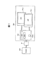
図1は、二枚の液晶パネルを用いた本発明の三次元画像表示装置の実施例1の構成を説明する図である。図1において、この三次元画像表示装置は、前側液晶表示パネルPNL1と後側液晶表示パネルPNL2とを所定の間隔で重ねて配置する。前側液晶表示パネルPNL1は表示部ARFを有し、後側液晶表示パネルPNL2には表示部ARRを有する。 FIG. 1 is a diagram for explaining a configuration of a first embodiment of a three-dimensional image display apparatus according to the present invention using two liquid crystal panels. In FIG. 1, the three-dimensional image display device includes a front side liquid crystal display panel PNL1 and a rear side liquid crystal display panel PNL2 that are stacked at a predetermined interval. The front liquid crystal display panel PNL1 has a display unit ARF, and the rear liquid crystal display panel PNL2 has a display unit ARR.
前側液晶表示パネルPNL1と後側液晶表示パネルPNL2には表示制御装置DSCが接続されており、二枚の液晶表示パネルとこの表示制御装置DSCとで表示モジュールMDLを構成している。 A display controller DSC is connected to the front liquid crystal display panel PNL1 and the rear liquid crystal display panel PNL2, and the two liquid crystal display panels and the display controller DSC constitute a display module MDL.
外部信号源SOCから入力する表示データは、赤、緑、青3色の各階調信号R,G,Bと深さ情報Zとから構成される。この表示データはインターフェース回路IFを介して表示モジュールMDLの表示制御装置DSCに入力する。表示モジュールMDLには、3色の各階調信号R,G,Bと深さ情報Zとから前側液晶表示パネルPNL1の表示部ARFに表示するための赤、緑、青3色の表示信号と後側液晶表示パネルの表示部に表示するための赤、緑、青3色の表示信号との二系統に展開する二画面表示信号生成回路CC1と、後側液晶表示パネルPNL2の表示部ARRに表示するための赤、緑、青3色の表示信号の解像度を変換する精細度変換回路CC2と、R,G,B信号を液晶表示パネルの画素回路を駆動する信号(TFT信号)に変換するTFT信号変換回路CC3、前側液晶表示パネルPNL1の表示部ARFと後側液晶表示パネルPNL2の表示部ARRの表示タイミングを生成するタイミングコントローラTCONとを有する。 Display data input from the external signal source SOC is composed of gradation signals R, G, B of three colors of red, green, and blue and depth information Z. This display data is input to the display controller DSC of the display module MDL via the interface circuit IF. In the display module MDL, display signals of three colors of red, green, and blue for display on the display portion ARF of the front liquid crystal display panel PNL1 from the three color gradation signals R, G, B and the depth information Z and the rear Displayed on the two-screen display signal generation circuit CC1 developed in two systems of red, green, and blue three-color display signals for display on the display section of the side liquid crystal display panel, and the display section ARR of the rear liquid crystal display panel PNL2. Definition conversion circuit CC2 that converts the resolution of the display signals of three colors red, green, and blue, and a TFT that converts the R, G, and B signals into signals (TFT signals) that drive the pixel circuits of the liquid crystal display panel The signal conversion circuit CC3, the display unit ARF of the front liquid crystal display panel PNL1, and the timing controller TCON that generates the display timing of the display unit ARR of the rear liquid crystal display panel PNL2.
実施例1では、外部信号源SOCから入力する各表示信号(階調信号)R,G,Bと深さ情報Zは、典型的には各6ビットであり、表示制御装置DSCでは入力したR,G,B及びZに基づいて前側液晶表示パネルPNL1と後側液晶表示パネルPNL2のそれぞれに与える表示信号R,G,Bを演算して振り分ける。また、精細度の高い後側液晶表示パネルPNL2への表示データは精細度変換回路CC2(スケーラ)で精細度を変換する。精細度の変換は、例えばバイリニア方式で行う。 In the first embodiment, the display signals (gradation signals) R, G, B and the depth information Z input from the external signal source SOC are typically 6 bits each, and the display controller DSC inputs R. , G, B, and Z are used to calculate and distribute display signals R, G, B applied to the front liquid crystal display panel PNL1 and the rear liquid crystal display panel PNL2, respectively. In addition, the display data on the rear liquid crystal display panel PNL2 having a high definition is converted by the definition conversion circuit CC2 (scaler). The definition conversion is performed by, for example, a bilinear method.
外部信号源SOCから入力する表示データはVGAであり、前側液晶表示パネルPNL1と同じである。したがって、精細度変換回路CC2は後側液晶表示パネルPNL2への表示信号をVGA→XGA変換する。 The display data input from the external signal source SOC is VGA, which is the same as that of the front liquid crystal display panel PNL1. Therefore, the definition conversion circuit CC2 converts the display signal to the rear liquid crystal display panel PNL2 from VGA to XGA.
図2は、液晶表示パネルの画素ピッチとモアレ波長の関係を説明する図である。モアレ(干渉縞)は二枚の液晶表示パネルの画素ピッチの比が1に近い場合に目立つ。一般的に、前側液晶表示パネルPNL1の画素ピッチをP1、後側液晶表示パネルPNL2の画素ピッチをP2、モアレ波長をPとすると、
1/P=?1/P1−1/P0?
の関係がある。
FIG. 2 is a diagram for explaining the relationship between the pixel pitch of the liquid crystal display panel and the moire wavelength. Moire (interference fringes) is conspicuous when the ratio of the pixel pitch of two liquid crystal display panels is close to 1. Generally, when the pixel pitch of the front liquid crystal display panel PNL1 is P1, the pixel pitch of the rear liquid crystal display panel PNL2 is P2, and the moire wavelength is P,
1 / P =? 1 / P1-1 / P0?
There is a relationship.
図2の横軸はP1/P0、縦軸はP/P0である。すなわち、横軸に二枚の液晶表示パネルPNL1とPNL2の画素ピッチの比を取り、縦軸にモアレ波長と後側液晶表示パネルPNL2の画素ピッチの比を取って、両比の関係を示した。 The horizontal axis in FIG. 2 is P1 / P0, and the vertical axis is P / P0. That is, the ratio of the pixel pitch of the two liquid crystal display panels PNL1 and PNL2 is taken on the horizontal axis, and the ratio of the moire wavelength and the pixel pitch of the rear liquid crystal display panel PNL2 is taken on the vertical axis to show the relationship between the two ratios. .
一般に、液晶表示パネルの画素ピッチは1mm以下で、例えばVGA精細度(460×640画素)のものでは0.33mmである。縦軸(P/P0)が5程度以下であれば、モアレピッチは1.65mm程度と小さく、モアレは気にならない。 In general, the pixel pitch of the liquid crystal display panel is 1 mm or less, for example, 0.33 mm for a VGA definition (460 × 640 pixels). If the vertical axis (P / P0) is about 5 or less, the moire pitch is as small as about 1.65 mm, and the moire is not a concern.
後側液晶表示パネルPNL2の精細度をQVGA(240×320画素)で、前側液晶表示パネルPNL1の精細度をVGA(460×640画素)とすると、P1/P0は1/2で、P/P0は1となり、モアレは目立たない。 When the definition of the rear liquid crystal display panel PNL2 is QVGA (240 × 320 pixels) and the definition of the front liquid crystal display panel PNL1 is VGA (460 × 640 pixels), P1 / P0 is 1/2 and P / P0 Becomes 1 and moire is not noticeable.
後側液晶表示パネルPNL2の精細度をVGA(460×640画素)で、前側液晶表示パネルPNL1の精細度をQVGA(240×320画素)とすると、P1/P0は2/1で、P/P0は2となり、モアレは目立たない。 When the definition of the rear liquid crystal display panel PNL2 is VGA (460 × 640 pixels) and the definition of the front liquid crystal display panel PNL1 is QVGA (240 × 320 pixels), P1 / P0 is 2/1 and P / P0 Becomes 2, and the moire is inconspicuous.
後側液晶表示パネルPNL2の精細度をVGA(460×640画素)で、前側液晶表示パネルPNL1の精細度をXGA(768×1024画素)とすると、P1/P0は1.6で、P/P0は2.7となり、モアレは目立たない。 If the definition of the rear liquid crystal display panel PNL2 is VGA (460 × 640 pixels) and the definition of the front liquid crystal display panel PNL1 is XGA (768 × 1024 pixels), P1 / P0 is 1.6 and P / P0 Becomes 2.7, and moire is inconspicuous.
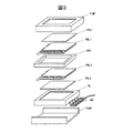
図3は、二枚の液晶表示パネルを観察側からみて垂直方向の前後に重ね合わせて立体画像表示を行うようにした三次元画像表示装置の構成例を説明する展開斜視図である。この三次元画像表示装置は、前側液晶表示パネルPNL1と後側液晶表示パネルPNL2をスペーサSPCを介して所定の間隔をもって重ね合わされている。前側液晶表示パネルPNL1の表面には偏光フィルムPOL1が貼付され、後側液晶表示パネルPNL2の背面には偏光フィルムPOL2が貼付されている。 FIG. 3 is an exploded perspective view illustrating a configuration example of a three-dimensional image display device in which two liquid crystal display panels are superimposed in front and rear in the vertical direction when viewed from the observation side to perform stereoscopic image display. In this three-dimensional image display device, the front side liquid crystal display panel PNL1 and the rear side liquid crystal display panel PNL2 are overlapped at a predetermined interval via a spacer SPC. A polarizing film POL1 is attached to the surface of the front liquid crystal display panel PNL1, and a polarizing film POL2 is attached to the back surface of the rear liquid crystal display panel PNL2.
後側液晶表示パネルPNL2の背面には照明装置(バックライト)BLが設置され、下側フレームFLM2と上側フレームFLM1とで表示装置を包み込んで一体化する筐体を構成する。また、この三次元画像表示装置では、その照明装置すなわちバックライトBLに1又は複数本の冷陰極蛍光灯を用いており、これに駆動電流を供給するインバータINVが設けられている。なお、このようなバックライトとしては、他に発光ダイオードを用いたものなどもある。 An illuminating device (backlight) BL is installed on the rear surface of the rear liquid crystal display panel PNL2, and the lower frame FLM2 and the upper frame FLM1 constitute a casing that wraps and integrates the display device. Further, in this three-dimensional image display device, one or a plurality of cold cathode fluorescent lamps are used for the illumination device, that is, the backlight BL, and an inverter INV for supplying a drive current thereto is provided. In addition, as such a backlight, there exist other things using a light emitting diode.
なお、上記の実施例では、表示装置として液晶表示パネルを二枚用いたもので説明したが、本発明はこれに限らず、一方の表示画像を他方の表示画像に重ねて一つの表示画像を生成できるもので、それらの表示領域に規則性を有する構造をもつものに対しても同様に適用できる。 In the above-described embodiment, the liquid crystal display panel is used as a display device. However, the present invention is not limited to this, and one display image is superimposed on the other display image. The present invention can be similarly applied to those having a structure having regularity in their display areas.
PNL1・・・前側液晶表示パネル、PNL2・・・後側液晶表示パネル、DSC・・・表示制御装置、MDL・・・表示モジュール、SOC・・・外部信号源、IF・・・インターフェース回路、CC1・・・二画面表示信号生成回路、CC2・・・精細度変換回路、TCON・・・タイミングコントローラ。
PNL1: front liquid crystal display panel, PNL2: rear liquid crystal display panel, DSC: display control device, MDL: display module, SOC: external signal source, IF: interface circuit, CC1 ... two-screen display signal generation circuit, CC2 ... definition conversion circuit, TCON ... timing controller.
Claims (10)
前記前側液晶表示パネルの表示部に表示される画像の精細度と前記後側液晶表示パネルの表示部に表示される画像の精細度とを異ならせたことを特徴とする三次元画像表示装置。 Two liquid crystal display panels superposed on each other at a predetermined interval, and a display control device for converting display data input from the outside into display signals to be displayed on the display units of the two liquid crystal display devices and supplying the display signals The two-dimensional image displayed on the display unit of the front liquid crystal display panel of the two liquid crystal display panels and the two-dimensional image displayed on the display unit of the rear liquid crystal display panel are superimposed to form a three-dimensional image. A three-dimensional image display device for generating an image,
3. A three-dimensional image display device, wherein the definition of an image displayed on the display unit of the front liquid crystal display panel is different from the definition of an image displayed on the display unit of the rear liquid crystal display panel.
前記前側液晶表示パネルの画素ピッチと前記後側液晶表示パネルの画素ピッチとが異なることを特徴とする三次元画像表示装置。 The three-dimensional image display device according to claim 1,
A three-dimensional image display device, wherein a pixel pitch of the front liquid crystal display panel and a pixel pitch of the rear liquid crystal display panel are different.
前記前側液晶表示パネルの画素ピッチの画素ピッチが、前記後側液晶表示パネルの画素ピッチよりも小であることを特徴とする三次元画像表示装置。 The three-dimensional image display device according to claim 2,
A three-dimensional image display device, wherein a pixel pitch of a pixel pitch of the front liquid crystal display panel is smaller than a pixel pitch of the rear liquid crystal display panel.
前記前側液晶表示パネルの画素ピッチの画素ピッチが、前記後側液晶表示パネルの画素ピッチよりも大であることを特徴とする三次元画像表示装置。 The three-dimensional image display device according to claim 2,
A three-dimensional image display device, wherein a pixel pitch of a pixel pitch of the front liquid crystal display panel is larger than a pixel pitch of the rear liquid crystal display panel.
前記表示制御装置に精細度変換回路を有し、前記前側液晶表示パネルの表示部と前記後側液晶表示パネルの表示部に精細度が異なる表示信号として供給することを特徴とする三次元画像表示装置。 The three-dimensional image display device according to claim 1,
A three-dimensional image display characterized by having a definition conversion circuit in the display control device and supplying the display unit of the front liquid crystal display panel and the display unit of the rear liquid crystal display panel as display signals having different definition. apparatus.
前記前側液晶表示パネルに供給する表示信号の精細度が、前記後側液晶表示パネルに供給する表示信号の精細度よりも高いことを特徴とする三次元画像表示装置。 The three-dimensional image display device according to claim 5,
A three-dimensional image display device, wherein a definition of a display signal supplied to the front liquid crystal display panel is higher than a definition of a display signal supplied to the rear liquid crystal display panel.
前記前側液晶表示パネルに供給する表示信号の精細度が、前記後側液晶表示パネルに供給する表示信号の精細度よりも低いことを特徴とする三次元画像表示装置。 The three-dimensional image display device according to claim 5,
A three-dimensional image display device, wherein a definition of a display signal supplied to the front liquid crystal display panel is lower than a definition of a display signal supplied to the rear liquid crystal display panel.
前記外部から入力する表示データは、赤、緑、青3色の各階調信号と深さ情報とから構成され、
前記表示制御装置に、前記3色の各階調信号と深さ情報とから前記前側液晶表示パネルの表示部に表示するための赤、緑、青3色の表示信号と、前記後側液晶表示パネルの表示部に表示するための赤、緑、青3色の表示信号とに展開する二画面表示信号生成回路と、
前記後側液晶表示パネルの表示部に表示するための赤、緑、青3色の表示信号の解像度を変換する精細度変換回路と、
前記前側液晶表示パネルの表示部と、前記後側液晶表示パネルの表示部の表示タイミングを生成するタイミングコントローラと、を備えたことを特徴とする三次元画像表示装置。 The three-dimensional image display device according to claim 1,
The display data input from the outside is composed of each gradation signal of red, green, and blue and depth information,
In the display control device, display signals of three colors of red, green, and blue for displaying on the display unit of the front liquid crystal display panel from the gradation signals and depth information of the three colors, and the rear liquid crystal display panel A two-screen display signal generation circuit that develops red, green, and blue three-color display signals for display on the display unit;
A definition conversion circuit that converts the resolution of display signals of three colors red, green, and blue for display on the display unit of the rear liquid crystal display panel;
A three-dimensional image display device comprising: a display unit of the front liquid crystal display panel; and a timing controller that generates display timing of the display unit of the rear liquid crystal display panel.
前記前側液晶表示パネルの解像度が、前記外部から入力する表示データの解像度と同じであることを特徴とする三次元画像表示装置。 The three-dimensional image display device according to claim 8,
3. The three-dimensional image display device according to claim 1, wherein a resolution of the front liquid crystal display panel is the same as a resolution of display data input from the outside.
3. A three-dimensional image display device, wherein the definition of the rear liquid crystal display panel is the same as the definition of display data input from the outside.
Priority Applications (1)
| Application Number | Priority Date | Filing Date | Title |
|---|---|---|---|
| JP2005330048A JP2007139865A (en) | 2005-11-15 | 2005-11-15 | Three-dimensional image display device |
Applications Claiming Priority (1)
| Application Number | Priority Date | Filing Date | Title |
|---|---|---|---|
| JP2005330048A JP2007139865A (en) | 2005-11-15 | 2005-11-15 | Three-dimensional image display device |
Publications (2)
| Publication Number | Publication Date |
|---|---|
| JP2007139865A true JP2007139865A (en) | 2007-06-07 |
| JP2007139865A5 JP2007139865A5 (en) | 2008-09-25 |
Family
ID=38202849
Family Applications (1)
| Application Number | Title | Priority Date | Filing Date |
|---|---|---|---|
| JP2005330048A Pending JP2007139865A (en) | 2005-11-15 | 2005-11-15 | Three-dimensional image display device |
Country Status (1)
| Country | Link |
|---|---|
| JP (1) | JP2007139865A (en) |
Cited By (6)
| Publication number | Priority date | Publication date | Assignee | Title |
|---|---|---|---|---|
| JP2007155780A (en) * | 2005-11-30 | 2007-06-21 | Fujitsu Ten Ltd | Display device |
| JP2009103866A (en) * | 2007-10-23 | 2009-05-14 | Seiko Epson Corp | Display device and electronic apparatus |
| JP4910076B1 (en) * | 2011-10-31 | 2012-04-04 | 健稔 岡本 | Information device, program for executing step of displaying display object and verification result of electronic signature of display object, and display method |
| WO2013054669A1 (en) * | 2011-10-13 | 2013-04-18 | 三洋電機株式会社 | Display device |
| CN103487980A (en) * | 2013-06-28 | 2014-01-01 | 友达光电股份有限公司 | Display device |
| US11579500B2 (en) | 2019-12-26 | 2023-02-14 | Shanghai Tianma Micro-electronics Co., Ltd. | Liquid crystal display device |
Citations (14)
| Publication number | Priority date | Publication date | Assignee | Title |
|---|---|---|---|---|
| JPS63100898A (en) * | 1986-10-17 | 1988-05-02 | Hitachi Ltd | Stereoscopic television set |
| JPS63144620A (en) * | 1986-12-08 | 1988-06-16 | Nippon Denso Co Ltd | Analog multiplexer circuit |
| JPH0588197A (en) * | 1991-09-30 | 1993-04-09 | Fuji Electric Co Ltd | Composite liquid crystal display panel device |
| JP2000206529A (en) * | 1999-01-19 | 2000-07-28 | Matsushita Electric Ind Co Ltd | Method to decrease moire fringe and liquid crystal display device |
| JP2002214566A (en) * | 2001-01-22 | 2002-07-31 | Nippon Telegr & Teleph Corp <Ntt> | Three-dimensional display method and apparatus |
| JP2003043449A (en) * | 2001-07-31 | 2003-02-13 | Optrex Corp | Liquid crystal display element |
| JP2003075774A (en) * | 2001-06-20 | 2003-03-12 | Nippon Telegr & Teleph Corp <Ntt> | Portable device |
| JP2004139056A (en) * | 2002-09-26 | 2004-05-13 | Sharp Corp | Transflective liquid crystal display panel, liquid crystal display panel and liquid crystal display |
| JP2004227978A (en) * | 2003-01-24 | 2004-08-12 | Pioneer Electronic Corp | Stereoscopic image display device |
| JP2004226796A (en) * | 2003-01-24 | 2004-08-12 | Pioneer Electronic Corp | Stereoscopic image display device |
| JP2004333869A (en) * | 2003-05-08 | 2004-11-25 | Nippon Telegr & Teleph Corp <Ntt> | Three-dimensional display device |
| JP2005017943A (en) * | 2003-06-27 | 2005-01-20 | Optrex Corp | Image display device |
| JP2005533275A (en) * | 2002-07-15 | 2005-11-04 | ピュアー デプス リミテッド | Improved multi-layer video screen |
| JP2007155780A (en) * | 2005-11-30 | 2007-06-21 | Fujitsu Ten Ltd | Display device |
-
2005
- 2005-11-15 JP JP2005330048A patent/JP2007139865A/en active Pending
Patent Citations (14)
| Publication number | Priority date | Publication date | Assignee | Title |
|---|---|---|---|---|
| JPS63100898A (en) * | 1986-10-17 | 1988-05-02 | Hitachi Ltd | Stereoscopic television set |
| JPS63144620A (en) * | 1986-12-08 | 1988-06-16 | Nippon Denso Co Ltd | Analog multiplexer circuit |
| JPH0588197A (en) * | 1991-09-30 | 1993-04-09 | Fuji Electric Co Ltd | Composite liquid crystal display panel device |
| JP2000206529A (en) * | 1999-01-19 | 2000-07-28 | Matsushita Electric Ind Co Ltd | Method to decrease moire fringe and liquid crystal display device |
| JP2002214566A (en) * | 2001-01-22 | 2002-07-31 | Nippon Telegr & Teleph Corp <Ntt> | Three-dimensional display method and apparatus |
| JP2003075774A (en) * | 2001-06-20 | 2003-03-12 | Nippon Telegr & Teleph Corp <Ntt> | Portable device |
| JP2003043449A (en) * | 2001-07-31 | 2003-02-13 | Optrex Corp | Liquid crystal display element |
| JP2005533275A (en) * | 2002-07-15 | 2005-11-04 | ピュアー デプス リミテッド | Improved multi-layer video screen |
| JP2004139056A (en) * | 2002-09-26 | 2004-05-13 | Sharp Corp | Transflective liquid crystal display panel, liquid crystal display panel and liquid crystal display |
| JP2004227978A (en) * | 2003-01-24 | 2004-08-12 | Pioneer Electronic Corp | Stereoscopic image display device |
| JP2004226796A (en) * | 2003-01-24 | 2004-08-12 | Pioneer Electronic Corp | Stereoscopic image display device |
| JP2004333869A (en) * | 2003-05-08 | 2004-11-25 | Nippon Telegr & Teleph Corp <Ntt> | Three-dimensional display device |
| JP2005017943A (en) * | 2003-06-27 | 2005-01-20 | Optrex Corp | Image display device |
| JP2007155780A (en) * | 2005-11-30 | 2007-06-21 | Fujitsu Ten Ltd | Display device |
Cited By (9)
| Publication number | Priority date | Publication date | Assignee | Title |
|---|---|---|---|---|
| JP2007155780A (en) * | 2005-11-30 | 2007-06-21 | Fujitsu Ten Ltd | Display device |
| JP2009103866A (en) * | 2007-10-23 | 2009-05-14 | Seiko Epson Corp | Display device and electronic apparatus |
| WO2013054669A1 (en) * | 2011-10-13 | 2013-04-18 | 三洋電機株式会社 | Display device |
| JP2013088465A (en) * | 2011-10-13 | 2013-05-13 | Sanyo Electric Co Ltd | Display device |
| JP4910076B1 (en) * | 2011-10-31 | 2012-04-04 | 健稔 岡本 | Information device, program for executing step of displaying display object and verification result of electronic signature of display object, and display method |
| CN103487980A (en) * | 2013-06-28 | 2014-01-01 | 友达光电股份有限公司 | Display device |
| JP2015011339A (en) * | 2013-06-28 | 2015-01-19 | 友達光電股▲ふん▼有限公司AU Optronics Corporation | Display device |
| TWI499838B (en) * | 2013-06-28 | 2015-09-11 | Au Optronics Corp | Display device |
| US11579500B2 (en) | 2019-12-26 | 2023-02-14 | Shanghai Tianma Micro-electronics Co., Ltd. | Liquid crystal display device |
Similar Documents
| Publication | Publication Date | Title |
|---|---|---|
| JP4823571B2 (en) | 3D display device | |
| JP5215261B2 (en) | Video display device | |
| JP4301565B2 (en) | Multiple view display | |
| CN102572478B (en) | Image display device | |
| JP4469930B2 (en) | Parallax barrier 3D image display device | |
| EP2682805A2 (en) | Multiple viewpoint image display device | |
| CN102340683B (en) | Image display device and driving method thereof | |
| JP2005134663A (en) | Multifunctional display device and switching liquid crystal panel for forming slit mask used for the device | |
| US8836775B2 (en) | Stereoscopic image display device and driving method thereof | |
| WO2009119279A1 (en) | Three-dimensional image display method and apparatus | |
| JP2007017768A (en) | Display device | |
| JP2008067092A (en) | Stereoscopic image display device and stereoscopic image display method | |
| JP2007163709A (en) | Stereoscopic image display apparatus | |
| CN102967940A (en) | Display device and electronic unit | |
| JP2007139865A (en) | Three-dimensional image display device | |
| KR100843097B1 (en) | Transparent display device and operation method for the same | |
| US20140146143A1 (en) | Stereoscopic image display device and method for driving the same | |
| KR102126532B1 (en) | Method of multi-view image formation and stereoscopic image display device using the same | |
| WO2020006847A1 (en) | Full-parallax switchable naked-eye 3d display device and display method thereof | |
| JP2005110022A (en) | Stereoscopic color image display device and color filter substrate | |
| CN201281790Y (en) | Liquid crystal display device and liquid crystal display panel | |
| JP2008299040A (en) | Image display device | |
| JP2009192897A (en) | Display device and stereoscopic display method | |
| US9137520B2 (en) | Stereoscopic image display device and method of displaying stereoscopic image | |
| KR20160021650A (en) | Lenticular lens type stereoscopic 3d display device |
Legal Events
| Date | Code | Title | Description |
|---|---|---|---|
| A521 | Written amendment |
Free format text: JAPANESE INTERMEDIATE CODE: A523 Effective date: 20080807 |
|
| A621 | Written request for application examination |
Free format text: JAPANESE INTERMEDIATE CODE: A621 Effective date: 20080807 |
|
| A711 | Notification of change in applicant |
Free format text: JAPANESE INTERMEDIATE CODE: A712 Effective date: 20110218 |
|
| RD03 | Notification of appointment of power of attorney |
Free format text: JAPANESE INTERMEDIATE CODE: A7423 Effective date: 20110218 |
|
| A977 | Report on retrieval |
Free format text: JAPANESE INTERMEDIATE CODE: A971007 Effective date: 20110506 |
|
| A131 | Notification of reasons for refusal |
Free format text: JAPANESE INTERMEDIATE CODE: A131 Effective date: 20110823 |
|
| A02 | Decision of refusal |
Free format text: JAPANESE INTERMEDIATE CODE: A02 Effective date: 20120117 |
|
| RD02 | Notification of acceptance of power of attorney |
Free format text: JAPANESE INTERMEDIATE CODE: A7422 Effective date: 20120330 |