US9107311B2 - Method for manufacturing printed circuit board - Google Patents
Method for manufacturing printed circuit board Download PDFInfo
- Publication number
- US9107311B2 US9107311B2 US13/858,102 US201313858102A US9107311B2 US 9107311 B2 US9107311 B2 US 9107311B2 US 201313858102 A US201313858102 A US 201313858102A US 9107311 B2 US9107311 B2 US 9107311B2
- Authority
- US
- United States
- Prior art keywords
- electrically conductive
- layer
- opening
- copper foil
- conductive circuit
- Prior art date
- Legal status (The legal status is an assumption and is not a legal conclusion. Google has not performed a legal analysis and makes no representation as to the accuracy of the status listed.)
- Active, expires
Links
Images


Classifications
-
- H—ELECTRICITY
- H05—ELECTRIC TECHNIQUES NOT OTHERWISE PROVIDED FOR
- H05K—PRINTED CIRCUITS; CASINGS OR CONSTRUCTIONAL DETAILS OF ELECTRIC APPARATUS; MANUFACTURE OF ASSEMBLAGES OF ELECTRICAL COMPONENTS
- H05K1/00—Printed circuits
- H05K1/02—Details
- H05K1/09—Use of materials for the conductive, e.g. metallic pattern
- H05K1/092—Dispersed materials, e.g. conductive pastes or inks
-
- H—ELECTRICITY
- H05—ELECTRIC TECHNIQUES NOT OTHERWISE PROVIDED FOR
- H05K—PRINTED CIRCUITS; CASINGS OR CONSTRUCTIONAL DETAILS OF ELECTRIC APPARATUS; MANUFACTURE OF ASSEMBLAGES OF ELECTRICAL COMPONENTS
- H05K3/00—Apparatus or processes for manufacturing printed circuits
- H05K3/10—Apparatus or processes for manufacturing printed circuits in which conductive material is applied to the insulating support in such a manner as to form the desired conductive pattern
-
- H—ELECTRICITY
- H05—ELECTRIC TECHNIQUES NOT OTHERWISE PROVIDED FOR
- H05K—PRINTED CIRCUITS; CASINGS OR CONSTRUCTIONAL DETAILS OF ELECTRIC APPARATUS; MANUFACTURE OF ASSEMBLAGES OF ELECTRICAL COMPONENTS
- H05K3/00—Apparatus or processes for manufacturing printed circuits
- H05K3/40—Forming printed elements for providing electric connections to or between printed circuits
- H05K3/42—Plated through-holes or plated via connections
- H05K3/425—Plated through-holes or plated via connections characterised by the sequence of steps for plating the through-holes or via connections in relation to the conductive pattern
- H05K3/427—Plated through-holes or plated via connections characterised by the sequence of steps for plating the through-holes or via connections in relation to the conductive pattern initial plating of through-holes in metal-clad substrates
-
- H—ELECTRICITY
- H05—ELECTRIC TECHNIQUES NOT OTHERWISE PROVIDED FOR
- H05K—PRINTED CIRCUITS; CASINGS OR CONSTRUCTIONAL DETAILS OF ELECTRIC APPARATUS; MANUFACTURE OF ASSEMBLAGES OF ELECTRICAL COMPONENTS
- H05K2201/00—Indexing scheme relating to printed circuits covered by H05K1/00
- H05K2201/01—Dielectrics
- H05K2201/0183—Dielectric layers
- H05K2201/0195—Dielectric or adhesive layers comprising a plurality of layers, e.g. in a multilayer structure
-
- H—ELECTRICITY
- H05—ELECTRIC TECHNIQUES NOT OTHERWISE PROVIDED FOR
- H05K—PRINTED CIRCUITS; CASINGS OR CONSTRUCTIONAL DETAILS OF ELECTRIC APPARATUS; MANUFACTURE OF ASSEMBLAGES OF ELECTRICAL COMPONENTS
- H05K2201/00—Indexing scheme relating to printed circuits covered by H05K1/00
- H05K2201/09—Shape and layout
- H05K2201/09009—Substrate related
- H05K2201/09036—Recesses or grooves in insulating substrate
-
- H—ELECTRICITY
- H05—ELECTRIC TECHNIQUES NOT OTHERWISE PROVIDED FOR
- H05K—PRINTED CIRCUITS; CASINGS OR CONSTRUCTIONAL DETAILS OF ELECTRIC APPARATUS; MANUFACTURE OF ASSEMBLAGES OF ELECTRICAL COMPONENTS
- H05K2201/00—Indexing scheme relating to printed circuits covered by H05K1/00
- H05K2201/09—Shape and layout
- H05K2201/09145—Edge details
-
- H—ELECTRICITY
- H05—ELECTRIC TECHNIQUES NOT OTHERWISE PROVIDED FOR
- H05K—PRINTED CIRCUITS; CASINGS OR CONSTRUCTIONAL DETAILS OF ELECTRIC APPARATUS; MANUFACTURE OF ASSEMBLAGES OF ELECTRICAL COMPONENTS
- H05K3/00—Apparatus or processes for manufacturing printed circuits
- H05K3/0011—Working of insulating substrates or insulating layers
- H05K3/0044—Mechanical working of the substrate, e.g. drilling or punching
- H05K3/005—Punching of holes
-
- H—ELECTRICITY
- H05—ELECTRIC TECHNIQUES NOT OTHERWISE PROVIDED FOR
- H05K—PRINTED CIRCUITS; CASINGS OR CONSTRUCTIONAL DETAILS OF ELECTRIC APPARATUS; MANUFACTURE OF ASSEMBLAGES OF ELECTRICAL COMPONENTS
- H05K3/00—Apparatus or processes for manufacturing printed circuits
- H05K3/22—Secondary treatment of printed circuits
- H05K3/28—Applying non-metallic protective coatings
- H05K3/281—Applying non-metallic protective coatings by means of a preformed insulating foil
-
- Y—GENERAL TAGGING OF NEW TECHNOLOGICAL DEVELOPMENTS; GENERAL TAGGING OF CROSS-SECTIONAL TECHNOLOGIES SPANNING OVER SEVERAL SECTIONS OF THE IPC; TECHNICAL SUBJECTS COVERED BY FORMER USPC CROSS-REFERENCE ART COLLECTIONS [XRACs] AND DIGESTS
- Y10—TECHNICAL SUBJECTS COVERED BY FORMER USPC
- Y10T—TECHNICAL SUBJECTS COVERED BY FORMER US CLASSIFICATION
- Y10T29/00—Metal working
- Y10T29/49—Method of mechanical manufacture
- Y10T29/49002—Electrical device making
- Y10T29/49117—Conductor or circuit manufacturing
- Y10T29/49124—On flat or curved insulated base, e.g., printed circuit, etc.
- Y10T29/49155—Manufacturing circuit on or in base
Definitions
- the present disclosure generally relates to printed circuit boards (PCBs), and particularly, relates to a printed circuit board and a method for manufacturing the printed circuit board.
- PCBs printed circuit boards
- a portion of the PCB may be a single layer circuit area.
- the single layer circuit area there is only one electrically conductive circuit layer.
- a substrate is obtained by laminating a single side copper clad laminate, an adhesive sheet, and a copper foil sheet. Before laminating, an opening spatially corresponding to the single layer circuit area is defined in the copper foil sheet and the adhesive sheet. Then, in an electroplating process, an electroplating copper layer may be formed on a surface of the single side copper clad laminate exposed from the single layer circuit area.
- a bonding force between the single side copper clad laminate and the electroplating copper layer is poor, and the electroplating copper layer damages easily.
- the damaged electroplating copper layer has liquid medicine, for example, copper plating liquid medicine, etching liquid medicine, but there is a slow drying process. Therefore, electrically conductive circuit traces adjacent to the single layer circuit area is easily oxidized, and a productivity of the PCB is lower
- FIG. 1 shows a copper foil substrate, an adhesive sheet, and a copper foil sheet according to an exemplary embodiment.
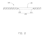
- FIG. 2 shows a first opening defined in the adhesive sheet in FIG. 1 .
- FIG. 3 is a top view of the adhesive sheet having the first opening.
- FIG. 4 shows a multilayer substrate including the copper foil substrate of FIG. 1 , the copper foil sheet of FIG. 1 and the adhesive sheet of FIG. 2 .
- FIG. 5 shows a through hole defined in the multilayer substrate of FIG. 4 .
- FIG. 6 shows an electrically conductive layer formed in the inner wall of the through hole of FIG. 5 .
- FIG. 7 shows a photoresist layer formed on the multilayer substrate of FIG. 6 .
- FIG. 8 shows an electrically conductive hole defined in the multilayer substrate of FIG. 7 .
- FIG. 9 shows electrically conductive circuit traces converted by the copper foil layer of copper foil substrate and the copper foil sheet of FIG. 8 .
- FIG. 10 is a cross-sectional view of a first printed circuit board, the printed circuit board comprises a first inner sidewall and a second inner sidewall.
- FIG. 11 shows a position relationship of a orthogonal projection of the first inner sidewall on the substrate layer and a orthogonal projection of the second inner sidewall on the substrate layer of FIG. 10 .
- FIG. 12 is a cross-section view of a second printed circuit board.
- FIG. 13 shows a position relationship of a orthogonal projection of the first inner sidewall on the substrate layer and a orthogonal projection of the second inner sidewall on the substrate layer of FIG. 12 .
- FIG. 14 is a cross-section view of a third printed circuit board.
- FIG. 15 shows a position relationship of a orthogonal projection of the first inner sidewall on the substrate layer and a orthogonal projection of the second inner sidewall on the substrate layer of FIG. 14 .
- a method for manufacturing a printed circuit board 100 includes the following steps.
- FIG. 1 shows step 1 , in which a single copper foil substrate 110 , an adhesive sheet 120 and a copper foil sheet 130 are provided.
- the single copper foil substrate 110 includes a copper foil layer 111 and a substrate layer 112 .
- a material of the substrate layer 112 may be polyimide.
- the adhesive sheet 120 may be a prepreg.
- the copper foil sheet 130 includes a removable area 131 and a circuit area 132 .
- the removable area 131 will be entirely removed in the following step.
- a shape of the removable area 131 is identical to a shaped of a single layer circuit area 100 b of the printed circuit board 100
- a size of the removable area 131 is identical to a size of the single layer circuit area 100 b of the printed circuit board 100 .
- the circuit area 132 surrounds the removable area 131 , and the circuit area 132 is configured for manufacturing electrically conductive layer.
- FIGS. 2 and 3 show step 2 , in which a first opening 121 is defined.
- the first opening 121 may be formed by a stamping method.
- a shape of the first opening 121 is similar to the shaped of the single layer circuit area of the printed circuit board, and a size of the first opening 121 is similar to a size of the single layer circuit area 100 b of the printed circuit board 100 .
- the shape of the first opening 121 is square.
- the shape of the first opening 12 may be polygonal, or round, for example.
- the adhesive sheet 120 includes a first inner sidewall 125 surrounding the first opening 121 .
- the first inner sidewall 125 includes a first side surface 122 , a second side surface (not shown), a third side surface 123 , and a fourth side surface (not shown), which are connected end to end.
- FIG. 4 shows step 3 , in which the adhesive sheet 120 is adhered between the substrate layer 112 and the copper foil sheet 130 , thereby obtaining a multilayer substrate 100 a.
- the first opening 121 spatially corresponds to the removable area 131 , and a portion of the substrate layer 112 , which is in the removable area 131 , is covered by the removable area 131 of the copper foil sheet 130 .
- FIGS. 5 to 8 show step 4 , in which at least one electrically conductive hole 104 is formed in the multilayer substrate 100 a .
- a through hole 101 is defined in the multilayer substrate 100 a .
- the through hole 101 passes through the multilayer substrate 100 a .
- the through hole 101 is defined in the circuit area 132 of the copper foil sheet 130 , and is separated from the first opening 121 . That is, the through hole 101 is not in the single layer circuit area 100 b of the printed circuit board 100 .
- the through hole 101 passes through the copper foil substrate 110 , the adhesive sheet 120 , and the copper foil sheet 130 .
- an electrically conductive layer 102 is formed on a portion of the substrate layer 112 and a portion of the adhesive sheet 120 , which are exposed in the through hole 101 .
- the electrically conductive layer 102 is formed by a black oxide treatment or a discolor hole method.
- a material of the electrically conductive layer 102 may be powdered carbon.
- a first photoresist pattern 141 is formed on the surface of the copper foil layer 111
- a second photoresist pattern 142 is formed on the surface of the copper foil sheet 130 .
- the first photoresist pattern 141 and the second photoresist pattern 142 may be formed by arranging a dry photoresist film on the surface of the copper foil layer 111 , exposing the dry photoresist film, and developing the dry photoresist film. A portion of the copper foil layer 111 surrounding the through hole 101 is exposed from the first photoresist pattern 141 , and the other portion of the copper foil layer 111 is covered by the first photoresist pattern 141 . A portion of the copper foil sheet 130 , which surrounds the through hole 101 , is exposed from the second photoresist pattern 142 , and the other portion of the copper foil sheet 130 , which is further from the through hole 101 , is covered by the second photoresist pattern 142 .
- an electroplating copper layer 103 is formed on the inner sidewall of the through hole 101 , the surface of the copper foil layer 111 , which is exposed from the first photoresist pattern 141 , and the surface of the copper foil sheet 130 , which is exposed from the second photoresist pattern 142 , thereby obtaining the electrically conductive hole 104 .
- the electroplating copper layer 103 is formed by an electroplating process.
- a portion of the electroplating copper layer 103 which is formed on the surface of the copper foil layer 111 exposed from the first photoresist pattern 141 , is a first annular ring 1041 .
- the first photoresist pattern 141 and the second photoresist pattern 142 are removed from the multilayer layer 100 a .
- the first photoresist pattern 141 and the second photoresist pattern 142 are removed by using a stripping solution.
- FIG. 9 shows step 5 , in which the copper foil layer 111 is converted into a first electrically conductive circuit pattern 113 by selectively etching, and the removal area 131 is removed by etching to form a second opening 133 .
- the copper foil sheet 130 is converted into a second electrically conductive circuit pattern 134 by selectively etching.
- a portion of the substrate layer 121 and a portion of the first electrically conductive circuit pattern 113 , both of which spatially correspond the first opening 121 cooperatively constitute the single layer circuit area 100 b.
- the first electrically conductive circuit pattern 113 , the second electrically conductive circuit pattern 134 , and the second opening 133 are formed by an image transfer process and an etching process.
- a shape of the second opening 133 substantially corresponds to the shape of the first opening 121
- a size of the second opening 133 is substantially corresponds to the size of the first opening 121 . Because the first opening 121 is formed by a stamping method, and the second opening 133 is formed by an image transfer process and an etching process, the first opening 121 and the second opening 133 are not parallel and level.
- an orthogonal projection of the first opening 121 on the substrate layer 112 at least partially overlaps but not completely overlap an orthogonal projection of the second opening 133 on the substrate layer 112 .
- the orthogonal projection of the first opening 121 on the substrate layer 112 may be within the orthogonal projection of the second opening 133 on the substrate layer 112 ; or the orthogonal projection of the second opening 133 on the substrate layer 112 may be within the orthogonal projection of the first opening 121 on the substrate layer 112 ; or the orthogonal projection of the first opening 121 on the substrate layer 112 may intersect the orthogonal projection of the second opening 133 on the substrate layer 112 .
- the shape of the first opening 121 may be identical to the shape of the second opening 133 ; the size of the first opening 121 may be slightly smaller or larger than the size of the second opening 133 , or the size of the first opening 121 may be identical to the size of the second opening 133 ; but the first opening 121 deviates from the second opening 133 .
- the second electrically conductive circuit pattern 134 in the position of the second opening 133 , includes a second inner sidewall 137 surrounding the second opening 133 .
- the second inner sidewall 137 includes a fifth side surface 135 , a sixth side surface (not shown), a seventh side surface 136 , and a eighth side surface (not shown), which are connected end to end.
- the fifth side surface 135 corresponds to the first side surface 122 ;
- the sixth side surface corresponds to the second side surface;
- the seventh side surface 136 corresponds to the third side surface 123 ;
- the eighth side surface corresponds to the fourth side surface.
- at least one group of the corresponding side surfaces are not in a same plane.
- first inner sidewall 125 and the second inner sidewall 137 are generally but not completely coplanar with each other. That is, an orthogonal projection of the first inner sidewall 125 on the substrate layer 112 at lease partially overlaps but not completely overlap an orthogonal projection of the second inner sidewall 137 on the substrate layer 112 .
- FIG. 10 shows step 6 , in which a first cover layer 151 is formed on a surface of a portion of the first electrically conductive circuit pattern 113 ; a second cover layer 152 is formed on a surface of the second electrically conductive circuit pattern 134 and a surface of the adhesive sheet 120 exposed from the second electrically conductive circuit pattern 134 .
- a cover layer film 1512 with an adhesive layer 1511 is adhered to the surface of a portion of the first electrically conductive circuit pattern 113 and a surface of the substrate layer 112 exposed from the first electrically conductive circuit pattern 113 , thereby obtaining the first cover layer 151 .
- a cover layer film 1522 with the adhesive layer 1521 is adhered to the surface of the second electrically conductive circuit pattern 134 and the surface of the adhesive sheet 120 exposed from the second electrically conductive circuit pattern 134 , thereby obtaining the second cover layer 152 .
- Step 7 in which a surface treatment is processed on the surface of the portion of the first electrically conductive circuit pattern 113 exposed from the first cover layer 151 .
- a nickel gold layer 114 (see FIG. 10 ) is formed on the surface of the portion of the first electrically conductive circuit pattern 113 exposed from the first cover layer 151 .
- the nickel gold layer 114 is configured for protecting the portion of the first electrically conductive circuit pattern 113 , and includes a nickel layer contacting with the first electrically conductive circuit pattern 113 and a gold layer formed on the nickel layer.
- the circuit board 100 includes the first electrically conductive circuit pattern 113 , the substrate layer 112 , the adhesive sheet 120 , and the second electrically conductive circuit pattern 134 , which are arranged in the above described order.
- the circuit board 100 includes a single layer circuit area 100 b and a double layer circuit area 100 c surrounding the single layer circuit area 100 b . In the single layer circuit area 100 b , there is only one electrically conductive circuit pattern. In the double layer electrically conductive circuit area 100 c , there are two electrically conductive circuit patterns.
- the first opening 121 spatially corresponding to the single layer circuit area 100 b is defined in the adhesive sheet 120 .
- the second opening 133 spatially corresponding to the single layer circuit area 100 b is defined in the second electrically conductive circuit pattern 134 .
- the orthogonal projection of the first opening 121 on the substrate layer 112 intersects the orthogonal projection of the second opening 133 on the substrate layer 112 . That is, the size of the first opening 121 may be slightly smaller or larger than the size of the second opening 133 , or the size of the first opening 121 may be identical to the size of the second opening 133 ; but the first opening 121 deviates from the second opening 133 .
- the adhesive sheet 120 includes the first inner sidewall 125 surrounding the first opening 121 .
- the first inner sidewall 125 includes the first side surface 122 , the second side surface, the third side surface 123 , and the fourth side surface (not shown).
- the second electrically conductive circuit pattern 134 includes the second inner sidewall 137 .
- the second inner sidewall 137 includes the fifth side surface 135 , the sixth side surface, the seventh side surface 136 , and the eighth side surface, which are connected end to end.
- the fifth side surface 135 corresponds to the first side surface 122 ; the sixth side surface corresponds to the second side surface; the seventh side surface 136 corresponds to the third side surface 123 ; the eighth side surface corresponds to the fourth side surface.
- at least one group of the corresponding side surfaces are not in a same plane. That is, an orthogonal projection of the first inner sidewall 125 on the substrate layer 112 at least partially overlaps but not completely overlap a orthogonal projection of the second inner sidewall 137 on the substrate layer 112 .
- FIGS. 10 and 11 show, when a cross section of the first opening 121 is smaller than a cross section of the second opening 133 , the orthogonal projection of the first opening 121 on the substrate layer 112 is in the orthogonal projection of the second opening 133 on the substrate layer 112 .
- the orthogonal projection of the second inner sidewall 137 on the substrate layer 112 surrounds the orthogonal projection of the first inner sidewall 125 on the substrate layer 112 .
- FIGS. 12 and 13 show, when the cross section of the first opening 121 is larger than the cross section of the second opening 133 , the orthogonal projection of the second inner sidewall 137 on the substrate layer 112 is within the orthogonal projection of the first inner sidewall 125 on the substrate layer 112 .
- FIGS. 14 and 15 show, when the cross section of the first opening 121 is equal to the cross section of the second opening 133 , the second opening 133 deviates from the first opening 121 .
- the orthogonal projection of the first opening 121 on the substrate layer 112 partially overlaps but not completely overlaps the orthogonal projection of the second opening 133 on the substrate 112 . That is, the orthogonal projection of the first opening 121 on the substrate layer 112 intersects the orthogonal projection of the second opening 137 .
- the electrically conductive hole 104 is formed.
- the electrically conductive hole 104 is configured for electrically connecting the first electrically conductive circuit pattern 113 and the second electrically conductive circuit pattern 134 .
- the printed circuit board 100 also includes the first cover layer 151 and the second cover layer 152 .
- the first cover layer 151 is formed on the surface of the portion of the electrically conductive circuit pattern 113 .
- the second cover layer 152 is formed on the second electrically conductive circuit pattern 134 and the surface of the adhesive sheet 120 exposed from the second electrically conductive circuit pattern 134 .
- the printed circuit board 100 also includes the nickel gold layer 114 .
- the nickel gold layer 114 is formed on the surface of the first electrically conductive circuit pattern 113 exposed from the first cover layer 151 .
- the nickel gold layer 114 is configured for protecting the portion of the first electrically conductive circuit pattern 113 , and includes a nickel layer contacting with the first electrically conductive circuit pattern 113 and a gold layer formed on the nickel layer.
- the copper foil layer can cover the substrate layer, such that the substrate layer cannot absorb electrically material, and the electroplating copper layer cannot be formed on the substrate layer in an electroplating process. Accordingly, the damage to the electroplating copper layer can be avoided, and the substrate layer can be easily dried. Therefore, electrically conductive circuit traces adjacent to the single layer circuit area is hardly oxidized, and a productivity of the PCB is higher.
Landscapes
- Engineering & Computer Science (AREA)
- Microelectronics & Electronic Packaging (AREA)
- Manufacturing & Machinery (AREA)
- Chemical & Material Sciences (AREA)
- Dispersion Chemistry (AREA)
- Production Of Multi-Layered Print Wiring Board (AREA)
- Printing Elements For Providing Electric Connections Between Printed Circuits (AREA)
Abstract
Description
Claims (4)
Applications Claiming Priority (2)
| Application Number | Priority Date | Filing Date | Title |
|---|---|---|---|
| CN2012103021087 | 2012-08-23 | ||
| CN201210302108.7A CN103635006B (en) | 2012-08-23 | 2012-08-23 | Circuit board and preparation method thereof |
Publications (2)
| Publication Number | Publication Date |
|---|---|
| US20140054074A1 US20140054074A1 (en) | 2014-02-27 |
| US9107311B2 true US9107311B2 (en) | 2015-08-11 |
Family
ID=50147008
Family Applications (1)
| Application Number | Title | Priority Date | Filing Date |
|---|---|---|---|
| US13/858,102 Active 2033-11-01 US9107311B2 (en) | 2012-08-23 | 2013-04-08 | Method for manufacturing printed circuit board |
Country Status (3)
| Country | Link |
|---|---|
| US (1) | US9107311B2 (en) |
| CN (1) | CN103635006B (en) |
| TW (1) | TWI462660B (en) |
Cited By (1)
| Publication number | Priority date | Publication date | Assignee | Title |
|---|---|---|---|---|
| US20230160764A1 (en) * | 2021-06-21 | 2023-05-25 | Avary Holding (Shenzhen) Co., Limited. | Pressure sensing circuit board and method for manufacturing the same |
Families Citing this family (3)
| Publication number | Priority date | Publication date | Assignee | Title |
|---|---|---|---|---|
| KR20160099381A (en) * | 2015-02-12 | 2016-08-22 | 삼성전기주식회사 | Printed circuit board and method of mamufacturing the same |
| TWI626872B (en) * | 2017-01-13 | 2018-06-11 | 元鼎音訊股份有限公司 | Printed circuit board manufacturing method and printed circuit board thereof |
| CN113966096A (en) * | 2021-09-26 | 2022-01-21 | 东莞康源电子有限公司 | Machining method of miniature flip-chip welding type cavity carrier plate |
Citations (7)
| Publication number | Priority date | Publication date | Assignee | Title |
|---|---|---|---|---|
| TW456162B (en) | 1998-06-05 | 2001-09-21 | Parlex Corp | Rigid/flex printed circuit board and manufacturing method therefor |
| US20030011075A1 (en) * | 2000-05-26 | 2003-01-16 | Tsutomu Ohuchi | Semiconductor package and production method thereof |
| US20030173664A1 (en) * | 2001-07-16 | 2003-09-18 | Ars Electronics Co., Ltd. | Semiconductor package and production method thereof |
| US20050155792A1 (en) * | 2002-02-22 | 2005-07-21 | Fujikura Ltd. | Multilayer wiring board, base for multilayer wiring board, printed wiring board and its manufacturing method |
| JP2006202891A (en) | 2005-01-19 | 2006-08-03 | Fujikura Ltd | Manufacturing method of rigid flex printed wiring board |
| US20070263370A1 (en) * | 2005-11-02 | 2007-11-15 | Ibiden Co., Ltd. | Multilayer printed wiring board for semiconductor devices and method for manufacturing the board |
| TW200826248A (en) | 2006-12-14 | 2008-06-16 | Ase Electronics Inc | Carrier and manufacturing process thereof |
Family Cites Families (5)
| Publication number | Priority date | Publication date | Assignee | Title |
|---|---|---|---|---|
| DE4003345C1 (en) * | 1990-02-05 | 1991-08-08 | Fa. Carl Freudenberg, 6940 Weinheim, De | |
| JP2006294862A (en) * | 2005-04-11 | 2006-10-26 | Fujikura Ltd | Wiring board manufacturing method and wiring board |
| CN201541388U (en) * | 2009-12-07 | 2010-08-04 | 昆山市线路板厂 | Double-side hollow flexible circuit board |
| CN102548253B (en) * | 2010-12-28 | 2013-11-06 | 富葵精密组件(深圳)有限公司 | Manufacturing method of multilayer circuit board |
| CN102559092A (en) * | 2012-01-09 | 2012-07-11 | 吴祖 | Circuit board conductive adhesive, single-sided and double-sided multi-layer printed circuit board and production method |
-
2012
- 2012-08-23 CN CN201210302108.7A patent/CN103635006B/en active Active
- 2012-08-30 TW TW101131602A patent/TWI462660B/en active
-
2013
- 2013-04-08 US US13/858,102 patent/US9107311B2/en active Active
Patent Citations (10)
| Publication number | Priority date | Publication date | Assignee | Title |
|---|---|---|---|---|
| TW456162B (en) | 1998-06-05 | 2001-09-21 | Parlex Corp | Rigid/flex printed circuit board and manufacturing method therefor |
| US20030011075A1 (en) * | 2000-05-26 | 2003-01-16 | Tsutomu Ohuchi | Semiconductor package and production method thereof |
| US20030173664A1 (en) * | 2001-07-16 | 2003-09-18 | Ars Electronics Co., Ltd. | Semiconductor package and production method thereof |
| US20050155792A1 (en) * | 2002-02-22 | 2005-07-21 | Fujikura Ltd. | Multilayer wiring board, base for multilayer wiring board, printed wiring board and its manufacturing method |
| JP2006202891A (en) | 2005-01-19 | 2006-08-03 | Fujikura Ltd | Manufacturing method of rigid flex printed wiring board |
| US20070263370A1 (en) * | 2005-11-02 | 2007-11-15 | Ibiden Co., Ltd. | Multilayer printed wiring board for semiconductor devices and method for manufacturing the board |
| US20100095523A1 (en) * | 2005-11-02 | 2010-04-22 | Ibiden Co., Ltd | Multilayer printed wiring board for semiconductor devices and method for manufacturing the board |
| US20110085306A1 (en) * | 2005-11-02 | 2011-04-14 | Ibiden Co., Ltd. | Multilayer printed wiring board for semiconductor devices and method for manufacturing the board |
| US20110220399A1 (en) * | 2005-11-02 | 2011-09-15 | Ibiden Co., Ltd. | Multilayer printed wiring board for semiconductor devices and method for manufacturing the board |
| TW200826248A (en) | 2006-12-14 | 2008-06-16 | Ase Electronics Inc | Carrier and manufacturing process thereof |
Cited By (2)
| Publication number | Priority date | Publication date | Assignee | Title |
|---|---|---|---|---|
| US20230160764A1 (en) * | 2021-06-21 | 2023-05-25 | Avary Holding (Shenzhen) Co., Limited. | Pressure sensing circuit board and method for manufacturing the same |
| US12320718B2 (en) * | 2021-06-21 | 2025-06-03 | Avary Holding (Shenzhen) Co., Limited. | Pressure sensing circuit board and method for manufacturing the same |
Also Published As
| Publication number | Publication date |
|---|---|
| CN103635006B (en) | 2016-09-28 |
| CN103635006A (en) | 2014-03-12 |
| TWI462660B (en) | 2014-11-21 |
| US20140054074A1 (en) | 2014-02-27 |
| TW201410086A (en) | 2014-03-01 |
Similar Documents
| Publication | Publication Date | Title |
|---|---|---|
| US9024203B2 (en) | Embedded printed circuit board and method for manufacturing same | |
| US9743533B2 (en) | Method for manufacturing rigid-flexible printed circuit board | |
| US8516694B2 (en) | Method for manufacturing printed circuit board with cavity | |
| US9357631B2 (en) | Flexible printed circuit board and method for making same | |
| US20140036465A1 (en) | Packaging substrate, method for manufacturing same, and chip packaging body having same | |
| US9730328B2 (en) | Printed circuit board with embedded component and method for manufacturing same | |
| US7799603B2 (en) | Method for mounting electronic component on printed circuit board | |
| US20140353006A1 (en) | Multilayer circuit board and method for manufacturing same | |
| US20140054079A1 (en) | Multilayer flexible printed circuit board and method for manufacturing same | |
| US8377317B2 (en) | Method for manufacturing printed circuit board with thick traces | |
| US20150053466A1 (en) | Printed circuit board and method for manufacturing same | |
| US9107311B2 (en) | Method for manufacturing printed circuit board | |
| TWI403244B (en) | Method for manufacturing multilayer printed circuit board | |
| CN102340933A (en) | How to make a circuit board | |
| US8674232B2 (en) | Device-embedded flexible printed circuit board and manufacturing method thereof | |
| US8067696B2 (en) | Printed circuit board and method for manufacturing same | |
| US20130092420A1 (en) | Embedded multilayer printed circuit board and method | |
| KR20170015626A (en) | Manufacturing method of printed circuit board | |
| US20080142249A1 (en) | Selective surface roughness for high speed signaling | |
| US20140110152A1 (en) | Printed circuit board and method for manufacturing same | |
| US20130220683A1 (en) | Printed circuit board and method for manufacturing printed circuit board | |
| KR101317597B1 (en) | Method for forming via hole and outer circuit layer of printed circuit board | |
| US20160081200A1 (en) | Method for manufacturing circuit board by etching polyimide | |
| KR101700161B1 (en) | Rigid-flexible boards in tape attached and Rigid-flexible boards manufacture method | |
| KR101154352B1 (en) | Imbeded printed circuit board member and manufacturing method the same and imbeded printed circuit board using the same |
Legal Events
| Date | Code | Title | Description |
|---|---|---|---|
| AS | Assignment |
Owner name: ZHEN DING TECHNOLOGY CO., LTD., TAIWAN Free format text: ASSIGNMENT OF ASSIGNORS INTEREST;ASSIGNORS:SHEN, FU-YUN;WANG, ZHI-TIAN;MING, BO;REEL/FRAME:030164/0907 Effective date: 20130401 Owner name: FUKUI PRECISION COMPONENT (SHENZHEN) CO., LTD., CH Free format text: ASSIGNMENT OF ASSIGNORS INTEREST;ASSIGNORS:SHEN, FU-YUN;WANG, ZHI-TIAN;MING, BO;REEL/FRAME:030164/0907 Effective date: 20130401 |
|
| STCF | Information on status: patent grant |
Free format text: PATENTED CASE |
|
| AS | Assignment |
Owner name: FUKUI PRECISION COMPONENT (SHENZHEN) CO., LTD., CH Free format text: ASSIGNMENT OF ASSIGNORS INTEREST;ASSIGNORS:FUKUI PRECISION COMPONENT (SHENZHEN) CO., LTD.;ZHEN DING TECHNOLOGY CO., LTD.;REEL/FRAME:040978/0802 Effective date: 20170101 Owner name: GARUDA TECHNOLOGY CO., LTD, TAIWAN Free format text: ASSIGNMENT OF ASSIGNORS INTEREST;ASSIGNORS:FUKUI PRECISION COMPONENT (SHENZHEN) CO., LTD.;ZHEN DING TECHNOLOGY CO., LTD.;REEL/FRAME:040978/0802 Effective date: 20170101 |
|
| AS | Assignment |
Owner name: AVARY HOLDING (SHENZHEN) CO., LIMITED., CHINA Free format text: CHANGE OF NAME;ASSIGNOR:FUKUI PRECISION COMPONENT (SHENZHEN) CO., LTD.;REEL/FRAME:043312/0632 Effective date: 20170524 |
|
| AS | Assignment |
Owner name: AVARY HOLDING (SHENZHEN) CO., LIMITED., CHINA Free format text: CHANGE OF NAME;ASSIGNOR:FUKUI PRECISION COMPONENT (SHENZHEN) CO., LTD.;REEL/FRAME:043378/0038 Effective date: 20170524 |
|
| MAFP | Maintenance fee payment |
Free format text: PAYMENT OF MAINTENANCE FEE, 4TH YEAR, LARGE ENTITY (ORIGINAL EVENT CODE: M1551); ENTITY STATUS OF PATENT OWNER: LARGE ENTITY Year of fee payment: 4 |
|
| MAFP | Maintenance fee payment |
Free format text: PAYMENT OF MAINTENANCE FEE, 8TH YEAR, LARGE ENTITY (ORIGINAL EVENT CODE: M1552); ENTITY STATUS OF PATENT OWNER: LARGE ENTITY Year of fee payment: 8 |