US9102129B2 - Spin-on carbon compositions for lithographic processing - Google Patents
Spin-on carbon compositions for lithographic processing Download PDFInfo
- Publication number
- US9102129B2 US9102129B2 US14/461,109 US201414461109A US9102129B2 US 9102129 B2 US9102129 B2 US 9102129B2 US 201414461109 A US201414461109 A US 201414461109A US 9102129 B2 US9102129 B2 US 9102129B2
- Authority
- US
- United States
- Prior art keywords
- bis
- carbon
- weight
- layer
- dianhydride
- Prior art date
- Legal status (The legal status is an assumption and is not a legal conclusion. Google has not performed a legal analysis and makes no representation as to the accuracy of the status listed.)
- Active
Links
- FAUAZXVRLVIARB-UHFFFAOYSA-N C1=CC(N(CC2CO2)CC2CO2)=CC=C1CC1=CC=C(N(CC2CO2)CC2CO2)C=C1 Chemical compound C1=CC(N(CC2CO2)CC2CO2)=CC=C1CC1=CC=C(N(CC2CO2)CC2CO2)C=C1 FAUAZXVRLVIARB-UHFFFAOYSA-N 0.000 description 3
- QCTCEWAOOTZJQU-UHFFFAOYSA-N C.C.C.C1CCC1.CCC.CCC.O=C=O.[H]C1C(C(C)=O)C(C(C)=O)C1C(=O)O.[Y] Chemical compound C.C.C.C1CCC1.CCC.CCC.O=C=O.[H]C1C(C(C)=O)C(C(C)=O)C1C(=O)O.[Y] QCTCEWAOOTZJQU-UHFFFAOYSA-N 0.000 description 2
- VJFXFRWTRVCQRU-UHFFFAOYSA-N C.C1CCC1.C1CCC1.[Y] Chemical compound C.C1CCC1.C1CCC1.[Y] VJFXFRWTRVCQRU-UHFFFAOYSA-N 0.000 description 2
- 0 *C.*C.*C.*C.*C.C1=CC=C(C2=CC=CC=C2)C=C1.C1=CC=C(CC2=CC=CC=C2)C=C1.C1=CC=CC=C1.CCC.CCC.CCC.CCC.CCC.CCCCC.CNC Chemical compound *C.*C.*C.*C.*C.C1=CC=C(C2=CC=CC=C2)C=C1.C1=CC=C(CC2=CC=CC=C2)C=C1.C1=CC=CC=C1.CCC.CCC.CCC.CCC.CCC.CCCCC.CNC 0.000 description 1
- MKAHBJZDQJFLSG-UHFFFAOYSA-N C=COCCCCOC(=O)C1=CC(C(=O)OCCCCOC=C)=CC(C(=O)OCCCCOC=C)=C1 Chemical compound C=COCCCCOC(=O)C1=CC(C(=O)OCCCCOC=C)=CC(C(=O)OCCCCOC=C)=C1 MKAHBJZDQJFLSG-UHFFFAOYSA-N 0.000 description 1
- UZEGFMNMJFPQIA-UHFFFAOYSA-N CC1=CC(C2CC(=O)OC2=O)CC2C(=O)OC(=O)C12.CCC1=CC=C(C2(C3=CC=C(CC(=O)C4C(C)=CC(C(CC(=O)O)C(C)=O)CC4C(=O)O)C=C3)C3=CC=CC=C3C3=C2C=CC=C3)C=C1.NC1=CC=C(C2(C3=CC=C(N)C=C3)C3=C(C=CC=C3)C3=C/C=C/C=C\32)C=C1 Chemical compound CC1=CC(C2CC(=O)OC2=O)CC2C(=O)OC(=O)C12.CCC1=CC=C(C2(C3=CC=C(CC(=O)C4C(C)=CC(C(CC(=O)O)C(C)=O)CC4C(=O)O)C=C3)C3=CC=CC=C3C3=C2C=CC=C3)C=C1.NC1=CC=C(C2(C3=CC=C(N)C=C3)C3=C(C=CC=C3)C3=C/C=C/C=C\32)C=C1 UZEGFMNMJFPQIA-UHFFFAOYSA-N 0.000 description 1
- RPNQITWCYTWQBT-UHFFFAOYSA-N CCC1=CC=C(C2(C3=CC=C(CC(=O)C4=CC(C(C)=O)=C(C(=O)O)C=C4C(=O)O)C=C3)C3=CC=CC=C3C3=C2C=CC=C3)C=C1.NC1=CC=C(C2(C3=CC=C(N)C=C3)C3=C(C=CC=C3)C3=C\C=C/C=C\32)C=C1.O=C1OC(=O)C2=CC3=C(C=C12)C(=O)OC3=O Chemical compound CCC1=CC=C(C2(C3=CC=C(CC(=O)C4=CC(C(C)=O)=C(C(=O)O)C=C4C(=O)O)C=C3)C3=CC=CC=C3C3=C2C=CC=C3)C=C1.NC1=CC=C(C2(C3=CC=C(N)C=C3)C3=C(C=CC=C3)C3=C\C=C/C=C\32)C=C1.O=C1OC(=O)C2=CC3=C(C=C12)C(=O)OC3=O RPNQITWCYTWQBT-UHFFFAOYSA-N 0.000 description 1
- BCFXPDYPEFUKNH-UHFFFAOYSA-N CCC1=CC=C(C2(C3=CC=C(CC(=O)C4=CC=C(C(=O)C5=CC=C(C(=O)O)C(C(C)=O)=C5)C=C4C(=O)O)C=C3)C3=CC=CC=C3C3=C2C=CC=C3)C=C1.NC1=CC=C(C2(C3=CC=C(N)C=C3)C3=C(C=CC=C3)C3=C/C=C/C=C\32)C=C1.O=C1OC(=O)C2=CC(C(=O)C3=CC=C4C(=O)OC(=O)C4=C3)=CC=C12 Chemical compound CCC1=CC=C(C2(C3=CC=C(CC(=O)C4=CC=C(C(=O)C5=CC=C(C(=O)O)C(C(C)=O)=C5)C=C4C(=O)O)C=C3)C3=CC=CC=C3C3=C2C=CC=C3)C=C1.NC1=CC=C(C2(C3=CC=C(N)C=C3)C3=C(C=CC=C3)C3=C/C=C/C=C\32)C=C1.O=C1OC(=O)C2=CC(C(=O)C3=CC=C4C(=O)OC(=O)C4=C3)=CC=C12 BCFXPDYPEFUKNH-UHFFFAOYSA-N 0.000 description 1
- VUFSLGBOVYIGGU-UHFFFAOYSA-N CCC1=CC=C(C2(C3=CC=C(CC(=O)C4=CC=C(C(C5=CC=C(C(=O)O)C(C(C)=O)=C5)(C(F)(F)F)C(F)(F)F)C=C4C(=O)O)C=C3)C3=CC=CC=C3C3=C2C=CC=C3)C=C1.NC1=CC=C(C2(C3=CC=C(N)C=C3)C3=C(C=CC=C3)C3=C/C=C/C=C\32)C=C1.O=C1OC(=O)C2=CC(C(C3=CC=C4C(=O)OC(=O)C4=C3)(C(F)(F)F)C(F)(F)F)=CC=C12 Chemical compound CCC1=CC=C(C2(C3=CC=C(CC(=O)C4=CC=C(C(C5=CC=C(C(=O)O)C(C(C)=O)=C5)(C(F)(F)F)C(F)(F)F)C=C4C(=O)O)C=C3)C3=CC=CC=C3C3=C2C=CC=C3)C=C1.NC1=CC=C(C2(C3=CC=C(N)C=C3)C3=C(C=CC=C3)C3=C/C=C/C=C\32)C=C1.O=C1OC(=O)C2=CC(C(C3=CC=C4C(=O)OC(=O)C4=C3)(C(F)(F)F)C(F)(F)F)=CC=C12 VUFSLGBOVYIGGU-UHFFFAOYSA-N 0.000 description 1
- UUOUGRUMSRMJHY-UHFFFAOYSA-N CCCCOCN1C(=O)N(COCCCC)C2C1N(COCCCC)C(=O)N2COCCCC Chemical compound CCCCOCN1C(=O)N(COCCCC)C2C1N(COCCCC)C(=O)N2COCCCC UUOUGRUMSRMJHY-UHFFFAOYSA-N 0.000 description 1
- SYOPFCKZTJCFHQ-UHFFFAOYSA-N O=C=O.O=C=O.O=C=O.O=C=O.O=C=O.O=C=O.O=C=O.[H]C(=O)C1=C(C(C)=O)C=C(C(C)=O)C(C(C)=O)=C1.[H]C(=O)C1=C(C(C)=O)C=CC(C(=O)C2=CC=C(C(C)=O)C(C(C)=O)=C2)=C1.[H]C(=O)C1=C(C(C)=O)C=CC(C(C)(C)C2=CC=C(C(C)=O)C(C(C)=O)=C2)=C1.[H]C(=O)C1=C(C(C)=O)C=CC(C(C2=CC=C(C(C)=O)C(C(C)=O)=C2)(C(F)(F)F)C(F)(F)F)=C1.[H]C(=O)C1=C(C(C)=O)C=CC(C2=CC=C(C(C)=O)C(C(C)=O)=C2)=C1.[H]C(=O)C1=C(C(C)=O)C=CC(S(=O)(=O)C2=CC=C(C(C)=O)C(C(C)=O)=C2)=C1.[H]C(=O)CC(CC(C)=O)(CC(C)=O)CC(C)=O Chemical compound O=C=O.O=C=O.O=C=O.O=C=O.O=C=O.O=C=O.O=C=O.[H]C(=O)C1=C(C(C)=O)C=C(C(C)=O)C(C(C)=O)=C1.[H]C(=O)C1=C(C(C)=O)C=CC(C(=O)C2=CC=C(C(C)=O)C(C(C)=O)=C2)=C1.[H]C(=O)C1=C(C(C)=O)C=CC(C(C)(C)C2=CC=C(C(C)=O)C(C(C)=O)=C2)=C1.[H]C(=O)C1=C(C(C)=O)C=CC(C(C2=CC=C(C(C)=O)C(C(C)=O)=C2)(C(F)(F)F)C(F)(F)F)=C1.[H]C(=O)C1=C(C(C)=O)C=CC(C2=CC=C(C(C)=O)C(C(C)=O)=C2)=C1.[H]C(=O)C1=C(C(C)=O)C=CC(S(=O)(=O)C2=CC=C(C(C)=O)C(C(C)=O)=C2)=C1.[H]C(=O)CC(CC(C)=O)(CC(C)=O)CC(C)=O SYOPFCKZTJCFHQ-UHFFFAOYSA-N 0.000 description 1
Images


Classifications
-
- C—CHEMISTRY; METALLURGY
- C09—DYES; PAINTS; POLISHES; NATURAL RESINS; ADHESIVES; COMPOSITIONS NOT OTHERWISE PROVIDED FOR; APPLICATIONS OF MATERIALS NOT OTHERWISE PROVIDED FOR
- C09D—COATING COMPOSITIONS, e.g. PAINTS, VARNISHES OR LACQUERS; FILLING PASTES; CHEMICAL PAINT OR INK REMOVERS; INKS; CORRECTING FLUIDS; WOODSTAINS; PASTES OR SOLIDS FOR COLOURING OR PRINTING; USE OF MATERIALS THEREFOR
- C09D179/00—Coating compositions based on macromolecular compounds obtained by reactions forming in the main chain of the macromolecule a linkage containing nitrogen, with or without oxygen, or carbon only, not provided for in groups C09D161/00 - C09D177/00
- C09D179/04—Polycondensates having nitrogen-containing heterocyclic rings in the main chain; Polyhydrazides; Polyamide acids or similar polyimide precursors
- C09D179/08—Polyimides; Polyester-imides; Polyamide-imides; Polyamide acids or similar polyimide precursors
-
- B—PERFORMING OPERATIONS; TRANSPORTING
- B32—LAYERED PRODUCTS
- B32B—LAYERED PRODUCTS, i.e. PRODUCTS BUILT-UP OF STRATA OF FLAT OR NON-FLAT, e.g. CELLULAR OR HONEYCOMB, FORM
- B32B33/00—Layered products characterised by particular properties or particular surface features, e.g. particular surface coatings; Layered products designed for particular purposes not covered by another single class
-
- B—PERFORMING OPERATIONS; TRANSPORTING
- B32—LAYERED PRODUCTS
- B32B—LAYERED PRODUCTS, i.e. PRODUCTS BUILT-UP OF STRATA OF FLAT OR NON-FLAT, e.g. CELLULAR OR HONEYCOMB, FORM
- B32B9/00—Layered products comprising a layer of a particular substance not covered by groups B32B11/00 - B32B29/00
- B32B9/04—Layered products comprising a layer of a particular substance not covered by groups B32B11/00 - B32B29/00 comprising such particular substance as the main or only constituent of a layer, which is next to another layer of the same or of a different material
-
- C—CHEMISTRY; METALLURGY
- C08—ORGANIC MACROMOLECULAR COMPOUNDS; THEIR PREPARATION OR CHEMICAL WORKING-UP; COMPOSITIONS BASED THEREON
- C08G—MACROMOLECULAR COMPOUNDS OBTAINED OTHERWISE THAN BY REACTIONS ONLY INVOLVING UNSATURATED CARBON-TO-CARBON BONDS
- C08G73/00—Macromolecular compounds obtained by reactions forming a linkage containing nitrogen with or without oxygen or carbon in the main chain of the macromolecule, not provided for in groups C08G12/00 - C08G71/00
- C08G73/06—Polycondensates having nitrogen-containing heterocyclic rings in the main chain of the macromolecule
- C08G73/10—Polyimides; Polyester-imides; Polyamide-imides; Polyamide acids or similar polyimide precursors
- C08G73/1067—Wholly aromatic polyimides, i.e. having both tetracarboxylic and diamino moieties aromatically bound
-
- C—CHEMISTRY; METALLURGY
- C08—ORGANIC MACROMOLECULAR COMPOUNDS; THEIR PREPARATION OR CHEMICAL WORKING-UP; COMPOSITIONS BASED THEREON
- C08G—MACROMOLECULAR COMPOUNDS OBTAINED OTHERWISE THAN BY REACTIONS ONLY INVOLVING UNSATURATED CARBON-TO-CARBON BONDS
- C08G73/00—Macromolecular compounds obtained by reactions forming a linkage containing nitrogen with or without oxygen or carbon in the main chain of the macromolecule, not provided for in groups C08G12/00 - C08G71/00
- C08G73/06—Polycondensates having nitrogen-containing heterocyclic rings in the main chain of the macromolecule
- C08G73/10—Polyimides; Polyester-imides; Polyamide-imides; Polyamide acids or similar polyimide precursors
- C08G73/1075—Partially aromatic polyimides
- C08G73/1078—Partially aromatic polyimides wholly aromatic in the diamino moiety
-
- G—PHYSICS
- G03—PHOTOGRAPHY; CINEMATOGRAPHY; ANALOGOUS TECHNIQUES USING WAVES OTHER THAN OPTICAL WAVES; ELECTROGRAPHY; HOLOGRAPHY
- G03F—PHOTOMECHANICAL PRODUCTION OF TEXTURED OR PATTERNED SURFACES, e.g. FOR PRINTING, FOR PROCESSING OF SEMICONDUCTOR DEVICES; MATERIALS THEREFOR; ORIGINALS THEREFOR; APPARATUS SPECIALLY ADAPTED THEREFOR
- G03F7/00—Photomechanical, e.g. photolithographic, production of textured or patterned surfaces, e.g. printing surfaces; Materials therefor, e.g. comprising photoresists; Apparatus specially adapted therefor
- G03F7/004—Photosensitive materials
- G03F7/09—Photosensitive materials characterised by structural details, e.g. supports, auxiliary layers
- G03F7/094—Multilayer resist systems, e.g. planarising layers
-
- H01L21/0332—
-
- H01L21/3081—
-
- H—ELECTRICITY
- H10—SEMICONDUCTOR DEVICES; ELECTRIC SOLID-STATE DEVICES NOT OTHERWISE PROVIDED FOR
- H10P—GENERIC PROCESSES OR APPARATUS FOR THE MANUFACTURE OR TREATMENT OF DEVICES COVERED BY CLASS H10
- H10P50/00—Etching of wafers, substrates or parts of devices
- H10P50/69—Etching of wafers, substrates or parts of devices using masks for semiconductor materials
- H10P50/691—Etching of wafers, substrates or parts of devices using masks for semiconductor materials for Group V materials or Group III-V materials
- H10P50/692—Etching of wafers, substrates or parts of devices using masks for semiconductor materials for Group V materials or Group III-V materials characterised by their composition, e.g. multilayer masks or materials
-
- H—ELECTRICITY
- H10—SEMICONDUCTOR DEVICES; ELECTRIC SOLID-STATE DEVICES NOT OTHERWISE PROVIDED FOR
- H10P—GENERIC PROCESSES OR APPARATUS FOR THE MANUFACTURE OR TREATMENT OF DEVICES COVERED BY CLASS H10
- H10P76/00—Manufacture or treatment of masks on semiconductor bodies, e.g. by lithography or photolithography
- H10P76/40—Manufacture or treatment of masks on semiconductor bodies, e.g. by lithography or photolithography of masks comprising inorganic materials
- H10P76/405—Manufacture or treatment of masks on semiconductor bodies, e.g. by lithography or photolithography of masks comprising inorganic materials characterised by their composition, e.g. multilayer masks
-
- B—PERFORMING OPERATIONS; TRANSPORTING
- B32—LAYERED PRODUCTS
- B32B—LAYERED PRODUCTS, i.e. PRODUCTS BUILT-UP OF STRATA OF FLAT OR NON-FLAT, e.g. CELLULAR OR HONEYCOMB, FORM
- B32B2255/00—Coating on the layer surface
- B32B2255/26—Polymeric coating
-
- B—PERFORMING OPERATIONS; TRANSPORTING
- B32—LAYERED PRODUCTS
- B32B—LAYERED PRODUCTS, i.e. PRODUCTS BUILT-UP OF STRATA OF FLAT OR NON-FLAT, e.g. CELLULAR OR HONEYCOMB, FORM
- B32B2307/00—Properties of the layers or laminate
- B32B2307/70—Other properties
-
- B—PERFORMING OPERATIONS; TRANSPORTING
- B32—LAYERED PRODUCTS
- B32B—LAYERED PRODUCTS, i.e. PRODUCTS BUILT-UP OF STRATA OF FLAT OR NON-FLAT, e.g. CELLULAR OR HONEYCOMB, FORM
- B32B2379/00—Other polymers having nitrogen, with or without oxygen or carbon only, in the main chain
- B32B2379/08—Polyimides
-
- Y—GENERAL TAGGING OF NEW TECHNOLOGICAL DEVELOPMENTS; GENERAL TAGGING OF CROSS-SECTIONAL TECHNOLOGIES SPANNING OVER SEVERAL SECTIONS OF THE IPC; TECHNICAL SUBJECTS COVERED BY FORMER USPC CROSS-REFERENCE ART COLLECTIONS [XRACs] AND DIGESTS
- Y10—TECHNICAL SUBJECTS COVERED BY FORMER USPC
- Y10T—TECHNICAL SUBJECTS COVERED BY FORMER US CLASSIFICATION
- Y10T428/00—Stock material or miscellaneous articles
- Y10T428/24—Structurally defined web or sheet [e.g., overall dimension, etc.]
- Y10T428/24802—Discontinuous or differential coating, impregnation or bond [e.g., artwork, printing, retouched photograph, etc.]
- Y10T428/24851—Intermediate layer is discontinuous or differential
-
- Y—GENERAL TAGGING OF NEW TECHNOLOGICAL DEVELOPMENTS; GENERAL TAGGING OF CROSS-SECTIONAL TECHNOLOGIES SPANNING OVER SEVERAL SECTIONS OF THE IPC; TECHNICAL SUBJECTS COVERED BY FORMER USPC CROSS-REFERENCE ART COLLECTIONS [XRACs] AND DIGESTS
- Y10—TECHNICAL SUBJECTS COVERED BY FORMER USPC
- Y10T—TECHNICAL SUBJECTS COVERED BY FORMER US CLASSIFICATION
- Y10T428/00—Stock material or miscellaneous articles
- Y10T428/30—Self-sustaining carbon mass or layer with impregnant or other layer
-
- Y—GENERAL TAGGING OF NEW TECHNOLOGICAL DEVELOPMENTS; GENERAL TAGGING OF CROSS-SECTIONAL TECHNOLOGIES SPANNING OVER SEVERAL SECTIONS OF THE IPC; TECHNICAL SUBJECTS COVERED BY FORMER USPC CROSS-REFERENCE ART COLLECTIONS [XRACs] AND DIGESTS
- Y10—TECHNICAL SUBJECTS COVERED BY FORMER USPC
- Y10T—TECHNICAL SUBJECTS COVERED BY FORMER US CLASSIFICATION
- Y10T428/00—Stock material or miscellaneous articles
- Y10T428/31504—Composite [nonstructural laminate]
- Y10T428/31551—Of polyamidoester [polyurethane, polyisocyanate, polycarbamate, etc.]
- Y10T428/31623—Next to polyamide or polyimide
-
- Y—GENERAL TAGGING OF NEW TECHNOLOGICAL DEVELOPMENTS; GENERAL TAGGING OF CROSS-SECTIONAL TECHNOLOGIES SPANNING OVER SEVERAL SECTIONS OF THE IPC; TECHNICAL SUBJECTS COVERED BY FORMER USPC CROSS-REFERENCE ART COLLECTIONS [XRACs] AND DIGESTS
- Y10—TECHNICAL SUBJECTS COVERED BY FORMER USPC
- Y10T—TECHNICAL SUBJECTS COVERED BY FORMER US CLASSIFICATION
- Y10T428/00—Stock material or miscellaneous articles
- Y10T428/31504—Composite [nonstructural laminate]
- Y10T428/31652—Of asbestos
- Y10T428/31667—Next to addition polymer from unsaturated monomers, or aldehyde or ketone condensation product
-
- Y—GENERAL TAGGING OF NEW TECHNOLOGICAL DEVELOPMENTS; GENERAL TAGGING OF CROSS-SECTIONAL TECHNOLOGIES SPANNING OVER SEVERAL SECTIONS OF THE IPC; TECHNICAL SUBJECTS COVERED BY FORMER USPC CROSS-REFERENCE ART COLLECTIONS [XRACs] AND DIGESTS
- Y10—TECHNICAL SUBJECTS COVERED BY FORMER USPC
- Y10T—TECHNICAL SUBJECTS COVERED BY FORMER US CLASSIFICATION
- Y10T428/00—Stock material or miscellaneous articles
- Y10T428/31504—Composite [nonstructural laminate]
- Y10T428/31678—Of metal
- Y10T428/31681—Next to polyester, polyamide or polyimide [e.g., alkyd, glue, or nylon, etc.]
-
- Y—GENERAL TAGGING OF NEW TECHNOLOGICAL DEVELOPMENTS; GENERAL TAGGING OF CROSS-SECTIONAL TECHNOLOGIES SPANNING OVER SEVERAL SECTIONS OF THE IPC; TECHNICAL SUBJECTS COVERED BY FORMER USPC CROSS-REFERENCE ART COLLECTIONS [XRACs] AND DIGESTS
- Y10—TECHNICAL SUBJECTS COVERED BY FORMER USPC
- Y10T—TECHNICAL SUBJECTS COVERED BY FORMER US CLASSIFICATION
- Y10T428/00—Stock material or miscellaneous articles
- Y10T428/31504—Composite [nonstructural laminate]
- Y10T428/31721—Of polyimide
Definitions
- the present invention relates to methods of forming a carbon-rich (spin-on carbon) layer from a polyamic acid for use in a multilayer stack and the microelectronic structures thereof.
- a single layer photoresist lacks sufficient thickness to complete pattern transfer to a substrate.
- trilayer stacking photoresist-hardmask-carbon layers
- the carbon layer can be formed by chemical vapor deposition (CVD) or spin-coating.
- CVD processes are expensive, have low-throughput, and subject the wafer to harsh conditions.
- epoxy cresol novolacs are the most common material for fabrication of spin-on carbon (“SOC”) layers, but this material has low thermal stability and low carbon content, leading to high sublimation and poor wiggling resistance during pattern transfer to silicon substrates. Additionally such a layer is difficult to remove after curing.
- SOC spin-on carbon
- Other SOC layers have been formed that are removable by dry etching. However, drying etching requires harsh processing conditions and special equipment, making the process less than desirable.
- the present invention provides a method of forming a microelectronic structure.
- the method comprises providing a substrate having a surface.
- one or more intermediate layers are formed on the surface, there being an uppermost intermediate layer on the surface, if one or more intermediate layers are present.
- a composition is applied to the uppermost intermediate layer, if present, or to the substrate surface, if no intermediate layers are present.
- the composition comprises a polyamic acid dissolved or dispersed in a solvent system.
- the composition is heated to form a spin-on carbon or carbon-rich layer, with the carbon-rich layer being developer soluble, and exhibiting a weight loss of less than about 10% at a temperature of about 400° C. for about 10 minutes.
- the invention also provides a novel microelectronic structure.
- the structure comprises a microelectronic substrate having a surface and optionally one or more intermediate layers on the surface. There is an uppermost intermediate layer on the surface, if one or more intermediate layers are present.
- a carbon-rich layer is on the uppermost intermediate layer, if present, or on the substrate surface, if no intermediate layers are present.
- the carbon-rich layer comprises a crosslinked polyamic acid; is developer soluble; and exhibits a weight loss of less than about 10% at a temperature of about 400° C. for about 10 minutes.
- FIG. (“FIG.”) 1 is a scanning electron microscope (“SEM”) photograph of the positive-tone development photolithography (40L/80P, 16.8 mJ) demonstrated in Example 26;
- FIG. 2 is an SEM photograph of the negative-tone development photolithography (53S/105P, 19.6 mJ) carried out in Example 27;
- FIG. 3 is an SEM photograph of the etched, spin-on carbon layer formed in Example 28;
- FIG. 4 shows the thermogravimetric analysis (“TGA”) curve of SOC formulation E-2 from Example 29;
- FIG. 5 is an SEM photograph of SOC formulation E-2 filling isolated deep contact hole, as described in Example 30;
- FIG. 6 is an SEM photograph of SOC formulation E-2 filling dense deep contact hole, as described in Example 30;
- FIG. 7 is an SEM photograph showing an OptiStack® SOC110D pattern after C 4 F 8 /Ar etching, as described in Example 32;
- FIG. 8 is an SEM photograph showing the pattern of Formulation E-2 after C 4 F 8 /Ar etching, as described in Example 33.
- the present invention provides methods of forming microelectronic structures and is particularly suited for multilayer processes.
- one or more optional intermediate layers are applied to the surface of a substrate.
- Suitable intermediate layers include those selected from the group consisting of spin-on hardmask, CVD hardmask, and spin-on carbon layers (without polyamic acids). Any conventional microelectronic substrate can be utilized.
- Preferred substrates include those selected from the group consisting of silicon, SiGe, SiO 2 , Si 3 N 4 , SiON, aluminum, tungsten, tungsten silicide, gallium arsenide, germanium, tantalum, tantalum nitride, coral, black diamond, phosphorous or boron doped glass, Ti 3 N 4 , hafnium, HfO 2 , ruthenium, indium phosphide, and mixtures of the foregoing.
- the substrate surface can be planar, or it can include topography features (via holes, trenches, contact holes, raised features, lines, etc.). As used herein, “topography” refers to the height or depth of a structure in or on a substrate surface.
- a polyamic acid composition is applied to uppermost intermediate layer, if present, or to the substrate surface, if no intermediate layers are present, to form a layer on the substrate surface.
- the composition can be applied by any known application method, with one preferred method being spin-coating the composition at speeds of from about 500 rpm to about 5,000 rpm (preferably from about 1,000 rpm to about 2,000 rpm) for a time period of from about 5 seconds to about 120 seconds (preferably from about 30 seconds to about 60 seconds). After the composition is applied, it is preferably heated to a temperature of from about 200° C. to about 450° C., and more preferably from about 205° C. to about 400° C.
- carbon-rich layer refers to layers comprising greater than about 50% by weight carbon, preferably greater than about 60% by weight carbon, more preferably greater than about 70% by weight carbon, and even more preferably from about 70% to about 99% by weight carbon, based upon the weight of the layer taken as 100% by weight.
- These carbon-rich layers will also preferably have a low hydrogen content (e.g., less than about 10% by weight hydrogen, preferably less than about 5% by weight hydrogen, more preferably less than about 3% by weight hydrogen, and even more preferably from about 0.010% to about 2% by weight hydrogen, based upon the weight of the layer taken as 100% by weight).
- a low hydrogen content e.g., less than about 10% by weight hydrogen, preferably less than about 5% by weight hydrogen, more preferably less than about 3% by weight hydrogen, and even more preferably from about 0.010% to about 2% by weight hydrogen, based upon the weight of the layer taken as 100% by weight).
- the average thickness of the carbon-rich layer (determined after baking) is preferably from about 0.05 ⁇ m to about 10 ⁇ m, more preferably from about 0.1 ⁇ m to about 5.0 ⁇ m, and even more preferably from about 0.1 ⁇ m to about 2.0 ⁇ m. If the substrate surface includes topography, the carbon-rich layer is preferably formed at a thickness sufficient to substantially cover the substrate topography and to achieve the above average thicknesses over the topography.
- the compositions used in the inventive methods exhibit excellent gap-fill properties and can fill deep contact holes very well.
- the dried or crosslinked carbon-rich layer can have a refractive index (n value) of at least about 1.40, preferably from about 1.45 to about 1.70, and more preferably from about 1.50 to about 1.65 at the wavelength of use (e.g., 365 nm, 248 nm, 193 nm, 157 nm, or 13.5 nm).
- n value refractive index
- the dried or crosslinked carbon-rich protective layer will be substantially insoluble in typical organic solvents used to form subsequent layers in the multilayer stack, such as propylene glycol methyl ether acetate (PGMEA), propylene glycol monomethyl ether (PGME), ethyl lactate, propylene glycol n-propyl ether, gamma-butyrolactone, cyclopentanone, cyclohexanone, n-butyl acetate, methyl isobutyl carbinol (MIBC), and mixtures thereof.
- PMEA propylene glycol methyl ether acetate
- PGME propylene glycol monomethyl ether
- ethyl lactate propylene glycol n-propyl ether
- gamma-butyrolactone cyclopentanone
- cyclohexanone cyclohexanone
- MIBC methyl isobutyl carbinol
- the stripping test involves first determining the thickness by taking the average of measurements at five different locations of the layer. This is the initial average film thickness. Next, the film is rinsed with a solvent (e.g., ethyl lactate) for about 30 seconds, followed by spin drying at about 500-3,000 rpm for about 20-60 seconds to remove the solvent. The thickness is measured again at those five points on the wafer using ellipsometry, and the average of these measurements is determined. This is the average final film thickness.
- a solvent e.g., ethyl lactate
- the amount of stripping is the difference between the initial and final average film thicknesses.
- the percent stripping is:
- % ⁇ ⁇ stripping ( amount ⁇ ⁇ of ⁇ ⁇ stripping initial ⁇ ⁇ average ⁇ ⁇ ⁇ film ⁇ ⁇ thickness ) ⁇ 100.
- the carbon-rich layer is soluble or capable of being rendered soluble in conventional aqueous developers (e.g., photoresist developers). That is, the term “developer-soluble” as used herein means that the carbon-rich layer is capable of being removed with conventional aqueous developers (e.g., hydroxides and/or any alkaline/base chemistry solutions). Particularly preferred developers are selected from the group consisting of tetramethyl ammonium hydroxide (TMAH), potassium hydroxide (KOH), sodium hydroxide, and mixtures thereof.
- TMAH tetramethyl ammonium hydroxide
- KOH potassium hydroxide
- sodium hydroxide and mixtures thereof.
- the carbon-rich layer advantageously can be removed during processing without dry etching (e.g., reactive ion etching), and is preferably not subjected to any dry etching in the method of the invention.
- the carbon-rich layer is preferably not photosensitive (i.e., a pattern cannot be defined in the layer when it is exposed to about 1 J/cm 2 ), and thus, photosensitive compositions such as photoresists or other imaging layers are not suitable for use as carbon-rich layers of the invention.
- the carbon-rich layer exhibits high thermal stability, making it particularly useful in high temperature processes such as deposition of an inorganic mask by CVD.
- the crosslinked polyamic acid layer can be heated at a higher temperature (i.e., from about 300° C. to about 450° C., and preferably from about 350° C. to about 400° C.) to promote imidization.
- the high thermal stability can be observed by TGA. Specifically, at a temperature of about 400° C. for about 10 minutes, the carbon-rich layer will experience a weight loss of less than about 10%, preferably less than about 5%, and preferably about 0%.
- the carbon-rich layers will also have low sublimation. At temperatures of from about 205° C. to about 225° C., and following the sublimation testing described in Example 31, carbon-rich layers according to the invention will have a sublimation of less than about 1,500 ng, preferably less than about 1,000 ng, and even more preferably less than about 500 ng.
- the carbon-rich layers form SOC patterns that minimize or prevent line deformation or line “wiggling.” Line wiggling is undesirable and prevents good pattern transfer to the underlaying layers and ultimately the substrate. Thus, improved patterning is achieved with the present invention.
- one or more additional intermediate layers can optionally be formed adjacent (i.e., on top of) the carbon-rich layer.
- additional intermediate layers include those selected from the group consisting of etch block layers, pattern transfer layers, and photoresists.
- the additional intermediate layer can be formed by any known application method, with one preferred method being spin-coating at speeds of from about 1,000 to about 5,000 rpm (preferably from about from about 1,250 to about 1,750 rpm) for a time period of from about 30 to about 120 seconds (preferably from about 45 to about 75 seconds).
- an intermediate etch block layer preferably comprises carbon compounds, metal compounds, or silicon compounds (e.g., Si 3 N 4 , SiO 2 , SiC, or SiON).
- the thickness of the etch block layer will vary, but is preferably from about 0.1 nm to about 100 nm, more preferably from about 1 nm to about 20 nm, and even more preferably from about 5 nm to about 10 nm.
- the most preferred intermediate layer is a pattern transfer layer (hardmask) formed adjacent the carbon-rich layer.
- the pattern transfer layer can be formed by any known application method, with one preferred method being spin-coating at speeds of from about 1,000 to about 5,000 rpm (preferably from about from about 1,000 to about 2,000 rpm) for a time period of from about 30 to about 120 seconds (preferably from about 45 to about 60 seconds). Chemical vapor deposition can also be used to form the pattern transfer layer.
- the pattern transfer layer can then be heated to a temperature of from about 100° C. to about 300° C., and more preferably from about 160° C. to about 205° C. and for a time period of from about 30 seconds to about 120 seconds (preferably from about 45 seconds to about 60 seconds) to evaporate solvents.
- the thickness of the pattern transfer layer after baking is preferably from about 1 nm to about 1,000 nm, more preferably from about 20 nm to about 100 nm, and even more preferably from about 30 nm to about 50 nm.
- Suitable compositions for use in forming the pattern transfer layer include hardmask materials (e.g., silicon- or metal-containing hardmasks and hybrid hardmasks) or spin-on glass materials (e.g., silicates, phosphosilicates, siloxanes).
- the imaging layer is then formed on the stack.
- the imaging layer can be formed by any known application method, with one preferred method being spin-coating at speeds of from about 500 to about 5,000 rpm (preferably from about from about 1,000 to about 2,000 rpm) for a time period of from about 30 to about 120 seconds (preferably from about 45 to about 60 seconds) onto the additional intermediate layers, if present, or onto the carbon-rich layer, if no additional intermediate layers are present.
- the imaging layer is post-application baked at a temperature of at least about 90° C., and preferably from about 90° C. to about 130° C., for time periods of from about 30 seconds to about 120 seconds (preferably 45 to about 60 seconds).
- Suitable imaging compositions include commercially-available photoresists (e.g., TArF Pi6-001 from TOK, Kawasaki shi, Kanagawa (Japan); ARX3001, ARX3340J, AM2073J, and KrFM592Y from JSR Micro, Sunnyvale, Calif.; SAIL-X-181, Shin-Etsu, Tokyo (Japan)) or any other photosensitive compositions.
- the inventive methods permit the use of much thinner imaging layers.
- the thickness of the imaging layer is less than about 500 nm, preferably less than about 300 nm, more preferably from about 50 nm to about 200 nm, and even more preferably from about 100 nm to about 180 nm. It will be appreciated that a conventional anti-reflective coating could also be present in the stack between the additional intermediate layer (or carbon-rich layer, if no additional intermediate level is present) and the imaging layer to control reflection during exposure of the imaging layer.
- the imaging layer can then be patterned by exposure to light of the appropriate wavelength. More specifically, the imaging layer is exposed using a mask positioned above the imaging layer.
- the mask has open areas designed to permit radiation (hv) to pass through the mask and contact the imaging layer.
- the remaining solid portions of the mask are designed to prevent radiation from contacting the imaging layer in certain areas.
- the arrangement of open areas and solid portions is designed based upon the desired pattern to be formed in the imaging layer and ultimately in the substrate.
- the imaging layer is preferably subjected to a post-exposure bake at a temperature of from about 90° C. to about 150° C., more preferably from about 110° C. to about 130° C., for a time period of from about 30 seconds to about 120 seconds.
- the portions of the imaging layer that are exposed to radiation are rendered soluble in aqueous developer.
- the exposed portions of the imaging layer that were made soluble by the above process are then contacted with an aqueous developer to remove the exposed portions to form the desired pattern in the imaging layer.
- the pattern can be via holes, trenches, lines, spaces, etc., that will ultimately be transferred to the substrate using an etch or ion implantation process or metal deposition.
- the exposed portions of the imaging layer can be rendered insoluble during the exposure process, in which case, the removal process is reversed from what is described above. That is, the unexposed portions are removed during development to form the pattern.
- Suitable developers are organic or inorganic alkaline solutions such as KOH or TMAH, and preferably comprise an aqueous solution of TMAH at a concentration of about 0.26N.
- Some of these developers are commercialized under the tradenames PD523AD (available from Moses Lake Industries, Inc., Moses Lake, Wash.), MF-319 (available from Shipley, Mass.), MF-320 (available from Shipley), and NMD3 (available from TOK, Japan).
- DSA Directed self-assembly
- an etching process is then used to transfer the pattern from the patterned imaging layer into the pattern transfer layer and/or other additional intermediate layer(s), if present.
- RIE is used to transfer the pattern using a reactive ion plasma of CF 4 , CHF 3 , O 2 , HBr, Cl 2 , SF 6 , C 2 F 6 , C 4 F 8 , CO, CO 2 , N 2 , H 2 , C 4 H 8 , Ar, N 2 H 2 , He, CH 2 F 2 , or a mixture thereof.
- Etching breaks through the additional intermediate layer(s) and exposes the developer-soluble, carbon-rich layer. The pattern is then transferred into the carbon-rich layer.
- the carbon-rich compositions utilized will comprise a polyamic acid dispersed or dissolved in a solvent system.
- the polyamic acid is preferably present in the composition at a level of from about 1% to about 30% by weight, preferably from about 2% to about 20% by weight, and more preferably from about 5% to about 15% by weight, based upon the total weight of solids in the composition taken as 100% by weight.
- the weight average molecular weight of the polyamic acid will preferably be less than about 15,000 Daltons, more preferably from about 4,000 Daltons to about 12,000 Daltons, and even more preferably from about 6,000 Daltons to about 11,000 Daltons.
- the polyamic acid should be selected to be a highly rigid structure. Ideally, the polyamic acid will have a flat or planar structure with limited spinning possible and a good deal of n bonding.
- the synthesis of these polyamic acids and suitable developer-soluble compositions comprising these polymers is described in U.S. Pat. Nos. 7,261,997 and 7,364,835, incorporated by reference herein in their entirety.
- the polyamic acids can be formed by adjusting the dianhydride-to-diamine ratio as well as the dianhydride and diamine types.
- the dianhydride can be aliphatic or aromatic.
- Typical aliphatic dianhydrides include those selected from the group consisting of 5-(2,5-dioxotetrahydrol)-3-methyl-3-cyclohexene-1,2-dicarboxylic acid anhydride, cyclobutane tetracarboxylic dianhydride, 1,2,3,4-cyclopentanetetracarboxylic acid dianhydride, tetrahydrofuran-2,3,4,5-tetracarboxylic dianhydride, 4-(2,5-dioxotetrahydrofuran-3-yl)-1,2,3,4-tetrahydronaphthalene-1,2-dicarboxylic anhydride, and bicyclo(2,2,2)oct-7-ene-2,3,5,6-tetracarboxylic dianhydride.
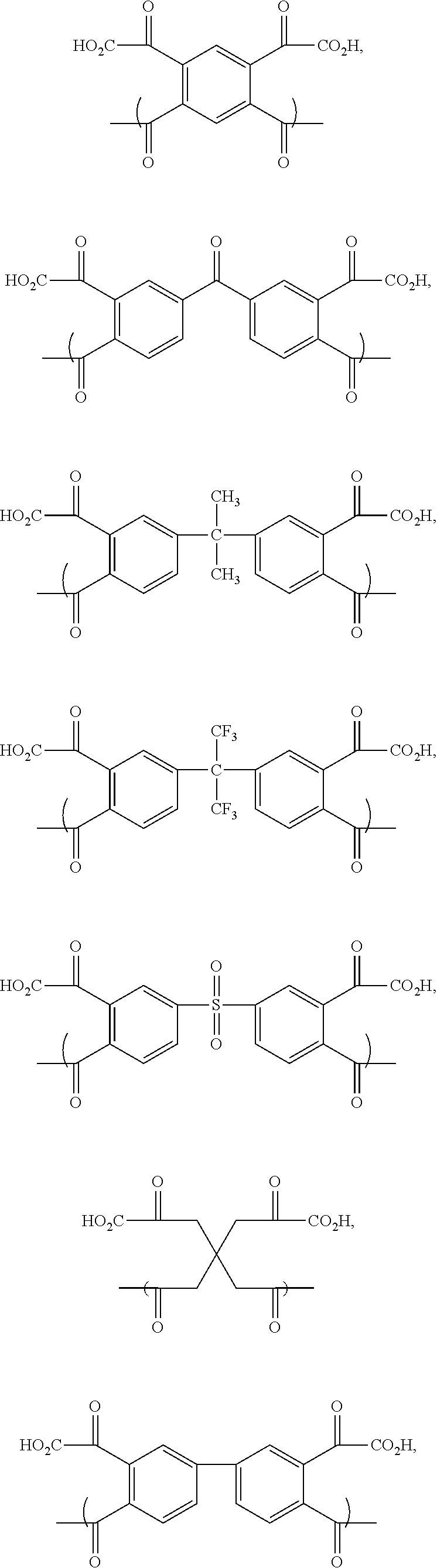
- Aromatic dianhydrides include those selected from the group consisting of 3,3′,4′-benzophenone tetracarboxylic acid dianhydride (BTDA), pyromellitic dianhydride (PMDA), 3,3′,4,4′-biphenyl tertracarboxylic dianhydride (s-BPDA), 2,2′-bis-(3,4-dicarboxy phenyl) hexafluoropropane dianhydride (6FDA), 4,4′-oxydiphthalic anhydride (OPDA), 3,3′,4,4′-diphenylsulfone tetracarboxylic dianhydride (DSDA), 4,4′-bisphenol A dianhydride (BPADA), hydroquinone diphtatic anhydride (HQDA), 3,4,9,10-perylene-tetracarboxylic dianhydride, 1,4,5,8-naphthalenetetracarboxylic dianhydride, and ethylene glycol bis(trim
- the diamine can also be aliphatic or aromatic.
- Typical aliphatic diamines include those selected from the group consisting of 1,3-bis(aminomethyl)-cyclohexane, 1,4-bis(aminimethyl)-cyclohexane, 4,4′-methylenebis(cyclohexylamine), and 4,4′-methylene bis(2-methylcyclohexyl)amine.
- Aromatic diamines include those selected from the group consisting of 3-aminobenzylamine, 1,3-bis(3-aminophenoxy)-benzene, 1,3-bis(4-aminophenoxy)-benzene, 1,4-bis(4-aminophenoxy)benzene, 4,4′-bis(4-aminophenoxy)-biphenyl, 2,2-bis[4-4-aminophenoxy)-phenyl]hexafluproprane, bis[4-(4-aminophenoxy)-phenyl]propane, bis[4-(4-aminophenoxy)-phenyl]sulfone, bis[4-(4-aminophenoxy)-phenyl]sulfone, 1,1′-bis(4-aminophenyl)-clohexane, 9,9′-bis(4-aminophenyl)-fluorene (FDA), 2,2′-bis(4-aminophenyl)-he
- Preferred polyamic acids include recurring monomers having the formulas
- X and Y groups include those selected from the group consisting of substituted and unsubstituted phenyl, biphenyl, naphthyl, and anthryl groups, and substituted and unsubstituted C 1 -C 2 aliphatic (preferably alkyl) groups.
- Particularly preferred polyamic acids for use in the composition comprise recurring monomers selected from the group consisting of
- X is selected from the group consisting of —O—, —S—, —CH 2 —, —C(CF 3 ) 2 —, and —C(CH 3 ) 2 —;
- n 2-8;
- each R is individually selected from the group consisting of —H and —OH.
- the preferred molar ratio of dianhydrides to diamines is from about 1.8:1 to about 1.05:1, more preferably from about 1.6:1 to about 1.1:1, and even more preferably from about 1.4:1 to about 1.2:1.
- the polyamic acid is also selected to be “carbon-rich.”
- carbon-rich polyamic acid refers to polyamic acids having greater than about 50% by weight carbon, preferably greater than about 60% by weight carbon, more preferably greater than about 70% by weight carbon atoms, and even more preferably from about 70% to about 99% by weight carbon, based upon the total weight of the polymer taken as 100% by weight.
- the preferred polyamic acid will also preferably have a low hydrogen content (e.g., less than about 10% by weight hydrogen, preferably less than about 5% by weight hydrogen, more preferably less than about 3% by weight hydrogen, and even more preferably from about 0.01% to about 2% by weight hydrogen, based upon the total weight of the polymer taken as 100% by weight).
- the carbon-rich compositions used in the invention also preferably include a crosslinking agent that will react with the carboxylic acid and/or the secondary amine.
- Epoxy crosslinking agents, vinyl ether crosslinking agents, and amino crosslinking agents are particularly preferred.
- Epoxy crosslinking agents include small molecules with multiple epoxy groups such as those selected from the group consisting of N,N,N′,N′-tetraglycidyl-4,4′-methylenebisbenzenamine, 4-glycidyloxy-N,N′-diglycidylaniline and bis(3,4-epoxy cyclo hexyl methyl)adipate, and polymers with epoxy groups, such as epoxy cresol novolac or polymers prepared from methylacrylate or acrylates with epoxy groups as side chains.
- Vinyl ether crosslinkers include multi functional vinyl ethers, such as those selected from the group consisting of 1,3,5-benzenetricarboxylic acid tris[4-(ethenyloxy)butyl]ester, bis[4-(vinyloxy)butyl]isophthalate, bis[4-(vinyloxy)butyl]1,6-hexanediylbiscarbamate, bis[4-(vinyloxymethyl)cyclohexylmethyl]glutarate, bis[4-(vinyloxy)butyl]succinate, tri(ethylene glycol)divinyl ether, and poly(ethylene glycol)divinyl ether.
- Amino resin crosslinkers include those selected from the group consisting of melamine crosslinkers, urea crosslinkers, benzoguanamine crosslinkers, and glycoluril crosslinkers.
- the crosslinking agent is preferably present in the composition at a level of from about 0.1% to about 30% by weight, preferably from about 0.5% to about 25% by weight, and more preferably from about 1% to about 20% by weight, based upon the total weight of solids in the composition taken as 100% by weight.
- Optional catalysts may include, but are not limited to, acids, such as 5-sulfosalicylic acid, thermally generated acid (TAG), photo generated acid (PAG), or base.
- Suitable surfactants include both ionic or nonionic surfactants.
- compositions are formed by simply dispersing or dissolving the polyamic acid in a suitable solvent system, preferably at ambient conditions and for a sufficient amount of time to form a substantially homogeneous dispersion.
- suitable solvent system preferably at ambient conditions and for a sufficient amount of time to form a substantially homogeneous dispersion.
- the other ingredients e.g., crosslinker, any catalysts and/or surfactants
- Preferred solvent systems include a solvent selected from the group consisting of PGMEA, PGME, propylene glycol n-propyl ether (PnP), ethyl lactate, cyclohexanone, gamma butyrolactone (GBL), and mixtures thereof.
- the solvent system should be utilized at a level of from about 80-99% by weight, and preferably from about 95-99% by weight, based upon the total weight of the composition taken as 100% by weight.
- the compositions typically have a solids content of from about 1-20% by weight, and preferably from about 1-5% by weight, based upon the total weight of the composition taken as 100% by weight.
- the resulting polyamic acid compositions will be carbon-rich.
- “Carbon-rich compositions” as used herein refers to compositions comprising greater than about 50% by weight carbon, preferably greater than about 60% by weight carbon, more preferably greater than about 70% by weight carbon, and even more preferably from about 70% to about 99% by weight carbon, based upon the total solids in the composition taken as 100% by weight.
- These polyamic acid compositions will also preferably have a low hydrogen content (e.g., less than about 10% by weight hydrogen, preferably less than about 5% by weight hydrogen, more preferably less than about 3% by weight hydrogen, and even more preferably from about 0.01% to about 2% by weight hydrogen, based upon the total solids in the composition taken as 100% by weight).
- An SOC formulation was prepared by mixing 5.01 grams of Polymer A from Example 1 with 0.114 gram of a 50% by weight solution of MY-720 (Huntsman Advanced Materials, Woodlands, Tex.) in PGME, 22.04 grams of PGME, and 2.92 grams of cyclohexanone to make a solution having a solids content of 3.5% by weight. The solution was mixed well for 4 hours and was filtered through a PTFE filter having a pore size of 0.1 ⁇ m. The formulation was spin-coated onto a 4-inch silicon wafer at 1,500 rpm for 60 seconds and then was baked on a hot plate at 225° C. for 60 seconds. The resulting cured film was measured by ellipsometry to be 1317 ⁇ thick and could not be removed by PGME or propylene glycol methyl ether acetate (“PGMEA”).
- An SOC formulation was prepared by mixing 5.01 grams of Polymer A from Example 1 with 0.206 gram of a 50% by weight solution of MY-720 in PGME, 23.25 grams of PGME, and 3.07 grams of cyclohexanone to make a solution having a solids content of 3.5% by weight. The solution was mixed well for 4 hours and then was filtered through a PTFE filter having a pore size of 0.1 ⁇ m. The formulation was spin-coated onto a 4-inch silicon wafer at 1,500 rpm for 60 seconds, and then was baked on a hot plate at 205° C. for 60 seconds. The resulting cured film was measured by ellipsometry to be 1,378 ⁇ thick and could not be removed by PGME or PGMEA.
- An SOC formulation was prepared by mixing 5.01 grams of Polymer B from Example 4 with 0.101 gram of a 50% by weight solution of MY-720 in PGME, 22.03 grams of PGME, and 2.92 grams of cyclohexanone to make a solution having a solids content of 3.5% by weight. The solution was mixed well for 4 hours and was filtered through a PTFE filter having a pore size of 0.1 ⁇ m. The formulation was spin-coated onto a 4-inch silicon wafer at 1,500 rpm for 60 seconds and then was baked on a hot plate at 205° C. for 60 seconds. The resulting cured film was measured by ellipsometry to be 1423 ⁇ thick and was unable to be removed by PGME and PGMEA.
- An SOC formulation was prepared by mixing 5.02 grams of Polymer B from Example 4 with 0.202 gram of a 50% by weight solution of MY-720 in PGME, 23.22 grams of PGME, and 3.03 grams of cyclohexanone to make a solution having a solids content of 3.5% by weight. The solution was mixed well for 4 hours and was filtered through a PTFE filter having a pore size of 0.1 ⁇ m. The formulation was spin-coated onto a 4-inch silicon wafer at 1,500 rpm for 60 seconds and then was baked on a hot plate at 205° C. for 60 seconds. The resulting cured film was measured by ellipsometry to be 1,422 ⁇ thick and could not be removed by PGME and PGMEA.
- An SOC formulation was prepared by mixing 9.08 grams of Polymer C from Example 7 with 0.36 gram of a 50% by weight solution of MY-720 in PGME, 35.75 grams of PGME, and 7.80 grams of cyclohexanone to make a solution having a solids content of 3.5% by weight.
- the solution was mixed well for 4 hours and was filtered through a PTFE filter having a pore size of 0.1 ⁇ m.
- the formulation was spin-coated onto a 4-inch silicon wafer at 1,500 rpm for 60 seconds and then was baked on a hot plate at 205° C. for 60 seconds. The resulting cured film was measured by ellipsometry to be 1,578 ⁇ thick and could not be removed by PGME and PGMEA.
- An SOC formulation was prepared by mixing 5.01 grams of Polymer D from Example 9 with 0.15 gram of a 50% by weight solution of MY-721 (Huntsman Advanced Materials, Woodlands, Tex.) in PGME, and 15.5 grams of PGME. The solution was mixed well for 4 hours and was filtered through a PTFE filter having a pore size of 0.1 ⁇ m. The formulation was spin-coated onto a 4-inch silicon wafer for 60 seconds and then was baked on a hot plate at 205° C. for 60 seconds.
- An SOC formulation was prepared by mixing 5.01 grams of Polymer E from Example 11 with 0.15 gram of a 50% by weight solution of MY-721 in PGME and 15.5 grams of PGME. The solution was mixed well for 4 hours and was filtered through a PTFE filter having a pore size of 0.1 ⁇ m. The formulation was spin-coated onto a 4-inch silicon wafer for 60 seconds and then was baked on a hot plate at 205° C. for 60 seconds.
- An SOC formulation was prepared by mixing 5.01 grams of Polymer E from Example 11 with 0.20 gram 1,3,5-benzenetricarboxylic acid tris[4-(ethenyloxy)butyl]ester crosslinker (structure shown below, Brewer Science Inc., Rolla, Mo.) and 15.5 grams of PGME. The solution was mixed well for 4 hours and was filtered through a PTFE filter having a pore size of 0.1 ⁇ m. The formulation was spin-coated onto a 4-inch silicon wafer for 60 seconds and then was baked on a hot plate at 225° C. for 60 seconds.
- An SOC formulation was prepared by mixing 5.01 grams of Polymer E from Example 11 with 0.20 gram Cymel 1174 crosslinker (structure shown below, Cytech Industries, Woodland Park, N.J.), 0.01 g TAG 2689 (thermal acid generator from King Industries, Norwalk, Conn.) in PGME, and 15.5 grams of PGME. The solution was mixed well for 4 hours and was filtered through a PTFE filter having a pore size of 0.1 ⁇ m. The formulation was spin-coated onto a 4-inch silicon wafer for 60 seconds and then baked on a hot plate at 205° C. for 60 seconds.
- An SOC formulation was prepared by mixing 5.01 grams of Polymer F from Example 15 with 0.15 gram of a 50% by weight solution of MY-721 in PGME and 15.5 grams of PGME. The solution was mixed well for 4 hours and was filtered through a PTFE filter having a pore size of 0.1 ⁇ m. The formulation was spin-coated onto a 4-inch silicon wafer for 60 seconds and then was baked on a hot plate at 205° C. for 60 seconds.
- An SOC formulation was prepared by mixing 5.01 grams of Polymer II from Example 18 with 0.05 gram of a 50% by weight solution of MY-721 (Huntsman Advanced Materials) in PGME, and 15.5 grams of PGME. The solution was mixed well for 4 hours and was filtered through a PTFE filter having a pore size of 0.1 ⁇ m. The formulation was spin-coated onto a 4 inch silicon wafer for 60 seconds and then was baked on a hot plate at 350° C. for 60 seconds. The highly thermal stable carbon layer formed according to the scheme shown below.
- An SOC formulation was prepared by mixing 5.01 grams of Polymer J from Example 21 with 0.15 gram of a 50% by weight solution of MY-721 in PGME and 15.5 grams of PGME. The solution was mixed well for 4 hours and was filtered through a PTFE filter having a pore size of 0.1 ⁇ m. The formulation was spin-coated onto a 4-inch silicon wafer at 1,500 rpm for 60 seconds and then was baked on a hot plate at 205° C. for 60 seconds.
- An SOC formulation was prepared by mixing 5.01 grams of Polymer K from Example 23 with 0.15 gram of a 50% by weight solution of MY-721 in PGME and 15.5 grams of PGME. The solution was mixed well for 4 hours and was filtered through a PTFE filter having a pore size of 0.1 ⁇ m. The formulation was spin-coated onto a 4-inch silicon wafer at 1500 rpm for 60 seconds and then was baked on a hot plate at 205° C. for 60 seconds.
- the optical constants (n and k) and film thickness were measured by M2000 Ellipsometer (J. A. Woollam, Lincoln, Nebr.).
- the coated wafer was puddled with the solvent for 20 seconds and spin-dried. The thickness before and after solvent contact was compared, and the results are listed in Table 1.
- the coated wafer was immersed in the developer PD523AD (Moses Chemicals Inc., Moses Lake, Wash.) at different temperatures for five minutes, and then rinsed by deionized water.
- Example 10 (SOC (SOC (SOC (SOC (SOC (SOC Formulation Formulation Formulation Formulation A-1) A-2) B-1) B-2) C-1) D-1) Optical n 193 nm 1.56 1.55 1.55 1.56 1.56 Constants k 193 nm 0.45 0.46 0.46 0.44 0.45 n 633 nm 1.61 1.62 1.62 1.61 1.61 k 633 nm 0.00 0.00 0.00 0.00 0.00 0.00 Stripping Loss in 0.0% 0.08% 25% 0.08% 0.3% 0.0% Loss PGME Loss in 0.0% 0.0% 0.0% 0.0% 0.0% 0.0% PGMEA Rework Rework Clean Residue NA Residue No Clean at room temp.
- a lithography test was performed using the following multilayer stack (from top to bottom): AIM54B4 (JSR Micro. Inc., Sunnyvale, Calif.) photoresist, OptiStack® HM9825 (Brewer Science Inc., Rolla, Mo.) hardmask, and SOC Formulation E-2 (Example 13) as the carbon layer.
- the coated wafer was exposed using a 1900i stepper (ASML, Veldhoven, Netherlands) and developed by an aqueous basic solution, OPD5262 (FujiFilm, North Kingstown, R.I.) to remove the exposed section.
- FIG. 1 demonstrates the lithography results.
- a lithography test was performed using the following stacking from the top to bottom: FAIRS9521-V10K (FujiFilm, North Kingstown, R.I.) photoresist; an experimental hardmask from Brewer Science Inc., Rolla, Mo.; and SOC Formulation E-2 (Example 13) as the carbon layer.
- the coated wafer was exposed using a 1900i stepper and developed using an organic developer, FN-DP001 (FujiFilm, North Kingstown, R.I.), to remove unexposed section.
- FIG. 2 demonstrates the lithography results.
- the wafer from Example 26 was cut into chips and then loaded at Oxford Plasmalab RIE for etching at following conditions: CF 4 , 35 sccm, 55 s, 50 mTorr, 100 W, followed by Ar/CO 2 , 25/25 sccm, 70 s, 20 mTorr, 300 W.
- the SEM photograph ( FIG. 3 ) demonstrated that the pattern of the photoresist was transferred to the SOC layer successfully.
- a film of Formulation E-2 (Example 13) was formed on a wafer and then was peeled from wafer and loaded into a TGA pan. The sample was heated to 400° C. at a speed of 20° C./min, and held for 10 minutes.
- FIG. 4 shows the curve of weight loss vs. time, which indicated that material exhibited an extremely high thermal stability at that temperature, similar to the temperatures at which CVD processes are carried out to deposit hardmasks on the SOC layer.
- SOC Formulations E-2 (Example 13) and E-3 (Example 14) were spin-coated on chips cut from Topowafer (SEMATECH, Albany, N.Y.) and baked at 225° C. SEM pictures ( FIGS. 5 and 6 ) demonstrate that deep contact holes (dense or isolated) are filled very well without any defects.
- Quartz crystal microbalance was used to determined the sublimation of samples.
- a quartz crystal is suspended over a hot place, where it can collect the outgassed material from heated wafer.
- a ventilation line is attached at the top to draw air flow upwards and allow the outgassed material to condense on the surface of the quartz crystal.
- the condensate is collected on the crystal, and the change in resonant frequency is correlated to mass units of the condensate.
- the standard process includes a 4-inch silicon wafer coated with an organic spin-on coating. The wafer was placed under the QCM on a hot place for 120 seconds. The data are collected.
- OptiStack® SOC110D (Brewer Science, Rolla, Mo.), Formulation E-1 (Example 12), and Formulation E-2 (Example 13) were spin-coated on a 4-inch silicon wafer and baked. The sublimation was collected for 120 seconds. The data are listed in Table 2, which demonstrated that the formulation exhibited comparable sublimation to current standard products, even when the baking temperature was higher.
- a lithography test was performed using the following multilayer stack (from top to bottom): AIM54B4 photoresist, OptiStack® HM825 hardmask, and OptiStack® SOC 110D as the carbon layer.
- the coated wafer was exposed using a 1900i stepper and developed by OPD5262 to remove the exposed section.
- the wafer was cut into chips and then loaded into an Oxford Plasmalab RIE for etching at following conditions: CF 4 , 35 sccm, 55 s, 50 mTorr, 100 W, followed by Ar/CO 2 , 25/25 sccm, 70 s, 20 mTorr, 300 W, and then C 4 F 8 /Ar, 5/100 sccm, 70 s, 20 mTorr, 300 W.
- FIG. 7 shows that the pattern of SOC layer wiggled during C 4 F 8 /Ar etching, and there was no good pattern transfer to silicon substrate.
- Example 26 The wafer from Example 26 was cut into chips and then loaded into an Oxford Plasmalab RIE for etching at following conditions: CF 4 , 35 sccm, 55 s, 50 mTorr, 100 W, followed by Ar/CO 2 , 25/25 sccm, 70 s, 20 mTorr, 300 W, and the C 4 F 8 /Ar, 5/100 sccm, 70 s, 20 mTorr, 300 W.
- FIG. 8 shows that the SOC pattern did not wiggle, which exhibited better wiggling resistance than current standard materials (Example 32). The pattern was transferred to the silicon substrate successfully.
Landscapes
- Chemical & Material Sciences (AREA)
- Chemical Kinetics & Catalysis (AREA)
- Organic Chemistry (AREA)
- Medicinal Chemistry (AREA)
- Polymers & Plastics (AREA)
- Health & Medical Sciences (AREA)
- Engineering & Computer Science (AREA)
- Materials Engineering (AREA)
- Life Sciences & Earth Sciences (AREA)
- Wood Science & Technology (AREA)
- Architecture (AREA)
- Structural Engineering (AREA)
- Physics & Mathematics (AREA)
- General Physics & Mathematics (AREA)
- Ceramic Engineering (AREA)
- Materials For Photolithography (AREA)
- Photosensitive Polymer And Photoresist Processing (AREA)
- Macromolecular Compounds Obtained By Forming Nitrogen-Containing Linkages In General (AREA)
- Exposure Of Semiconductors, Excluding Electron Or Ion Beam Exposure (AREA)
Abstract
Description

where each of
is individually selected from the group consisting of aliphatic and aryl groups. Particularly preferred X and Y groups include those selected from the group consisting of substituted and unsubstituted phenyl, biphenyl, naphthyl, and anthryl groups, and substituted and unsubstituted C1-C2 aliphatic (preferably alkyl) groups.

where:


| TABLE 1 | |||||||
| Example 2 | Example 3 | Example 5 | Example 6 | Example 8 | Example 10 | ||
| (SOC | (SOC | (SOC | (SOC | (SOC | (SOC | ||
| Formulation | Formulation | Formulation | Formulation | Formulation | Formulation | ||
| A-1) | A-2) | B-1) | B-2) | C-1) | D-1) | ||
| Optical | n193 nm | 1.56 | 1.55 | 1.55 | 1.56 | 1.56 | |
| Constants | k193 nm | 0.45 | 0.46 | 0.46 | 0.44 | 0.45 | |
| n633 nm | 1.61 | 1.62 | 1.62 | 1.61 | 1.61 | ||
| k633 nm | 0.00 | 0.00 | 0.00 | 0.00 | 0.00 | ||
| Stripping | Loss in | 0.0% | 0.08% | 25% | 0.08% | 0.3% | 0.0% |
| Loss | PGME | ||||||
| Loss in | 0.0% | 0.0% | 0.0% | 0.0% | 0.0% | 0.0% | |
| PGMEA | |||||||
| Rework | Rework | Clean | Residue | NA | Residue | No | Clean |
| at room | |||||||
| temp. | |||||||
| Rework | Residue | Residue | Residue | Residue | Clean | ||
| at 60° C. | |||||||
| Example 12 | Example 13 | Example 14 | Example 16 | Example 22 | Example 24 | ||
| (SOC | (SOC | (SOC | (SOC | (SOC | (SOC | ||
| Formulation | Formulation | Formulation | Formulation | Formulation | Formulation | ||
| E-1) | E-2) | E-3) | F-1) | J-1) | K-1) | ||
| Optical | n193 nm | 1.55 | 1.55 | 1.56 | 1.56 | ||
| Constants | k193 nm | 0.46 | 0.46 | 0.44 | 0.44 | ||
| n633 nm | 1.62 | 1.62 | 1.61 | 1.61 | |||
| k633 nm | 0.00 | 0.00 | 0.00 | 0.00 | |||
| Stripping | Loss in | 0.00% | 0.0% | 0.0% | 0.0% | 0.0% | 0.0% |
| Loss | PGME | ||||||
| Loss in | 0.0% | 0.0% | 0.0% | 0.0% | 0.0% | 0.0%) | |
| PGMEA | |||||||
| Rework | Rework | Clean | No | Clean | No | Clean | Clean |
| at room | |||||||
| temp. | |||||||
| Rework | Clean | Clean | |||||
| at 60° C. | |||||||
| TABLE 2 | ||
| Sample | Bake Temperature | Sublimation (ng) |
| OptiStack ® SOC110D | 205° C. | 1231 |
| Formulation E-1 | 205° C. | 385 |
| Formulation E-2 | 225° C. | 1392 |
Claims (12)

Priority Applications (1)
| Application Number | Priority Date | Filing Date | Title |
|---|---|---|---|
| US14/461,109 US9102129B2 (en) | 2011-10-10 | 2014-08-15 | Spin-on carbon compositions for lithographic processing |
Applications Claiming Priority (3)
| Application Number | Priority Date | Filing Date | Title |
|---|---|---|---|
| US201161545313P | 2011-10-10 | 2011-10-10 | |
| US13/648,890 US8895230B2 (en) | 2011-10-10 | 2012-10-10 | Spin-on carbon compositions for lithographic processing |
| US14/461,109 US9102129B2 (en) | 2011-10-10 | 2014-08-15 | Spin-on carbon compositions for lithographic processing |
Related Parent Applications (1)
| Application Number | Title | Priority Date | Filing Date |
|---|---|---|---|
| US13/648,890 Division US8895230B2 (en) | 2011-10-10 | 2012-10-10 | Spin-on carbon compositions for lithographic processing |
Publications (2)
| Publication Number | Publication Date |
|---|---|
| US20140356593A1 US20140356593A1 (en) | 2014-12-04 |
| US9102129B2 true US9102129B2 (en) | 2015-08-11 |
Family
ID=48042276
Family Applications (3)
| Application Number | Title | Priority Date | Filing Date |
|---|---|---|---|
| US13/648,890 Ceased US8895230B2 (en) | 2011-10-10 | 2012-10-10 | Spin-on carbon compositions for lithographic processing |
| US14/461,109 Active US9102129B2 (en) | 2011-10-10 | 2014-08-15 | Spin-on carbon compositions for lithographic processing |
| US15/360,385 Active USRE46841E1 (en) | 2011-10-10 | 2016-11-23 | Spin-on carbon compositions for lithographic processing |
Family Applications Before (1)
| Application Number | Title | Priority Date | Filing Date |
|---|---|---|---|
| US13/648,890 Ceased US8895230B2 (en) | 2011-10-10 | 2012-10-10 | Spin-on carbon compositions for lithographic processing |
Family Applications After (1)
| Application Number | Title | Priority Date | Filing Date |
|---|---|---|---|
| US15/360,385 Active USRE46841E1 (en) | 2011-10-10 | 2016-11-23 | Spin-on carbon compositions for lithographic processing |
Country Status (8)
| Country | Link |
|---|---|
| US (3) | US8895230B2 (en) |
| EP (1) | EP2766920B1 (en) |
| JP (1) | JP6295198B2 (en) |
| KR (1) | KR102058760B1 (en) |
| CN (1) | CN103975418B (en) |
| SG (2) | SG10201607603VA (en) |
| TW (1) | TWI582134B (en) |
| WO (1) | WO2013055798A1 (en) |
Cited By (4)
| Publication number | Priority date | Publication date | Assignee | Title |
|---|---|---|---|---|
| US10649328B2 (en) | 2016-03-11 | 2020-05-12 | Inpria Corporation | Pre-patterned lithography templates, processes based on radiation patterning using the templates and processes to form the templates |
| US11084032B2 (en) | 2018-08-28 | 2021-08-10 | International Business Machines Corporation | Method to create multilayer microfluidic chips using spin-on carbon as gap fill and spin-on glass tone inversion |
| US11192101B2 (en) | 2018-08-28 | 2021-12-07 | International Business Machines Corporation | Method to create multilayer microfluidic chips using spin-on carbon as gap filling materials |
| US11886116B2 (en) | 2020-05-06 | 2024-01-30 | Inpria Corporation | Multiple patterning with organometallic photopatternable layers with intermediate freeze steps |
Families Citing this family (379)
| Publication number | Priority date | Publication date | Assignee | Title |
|---|---|---|---|---|
| US10378106B2 (en) | 2008-11-14 | 2019-08-13 | Asm Ip Holding B.V. | Method of forming insulation film by modified PEALD |
| KR101156489B1 (en) * | 2008-12-02 | 2012-06-18 | 제일모직주식회사 | Hardmask composition having antireflective property |
| US9394608B2 (en) | 2009-04-06 | 2016-07-19 | Asm America, Inc. | Semiconductor processing reactor and components thereof |
| US8802201B2 (en) | 2009-08-14 | 2014-08-12 | Asm America, Inc. | Systems and methods for thin-film deposition of metal oxides using excited nitrogen-oxygen species |
| US9312155B2 (en) | 2011-06-06 | 2016-04-12 | Asm Japan K.K. | High-throughput semiconductor-processing apparatus equipped with multiple dual-chamber modules |
| US10364496B2 (en) | 2011-06-27 | 2019-07-30 | Asm Ip Holding B.V. | Dual section module having shared and unshared mass flow controllers |
| US10854498B2 (en) | 2011-07-15 | 2020-12-01 | Asm Ip Holding B.V. | Wafer-supporting device and method for producing same |
| US20130023129A1 (en) | 2011-07-20 | 2013-01-24 | Asm America, Inc. | Pressure transmitter for a semiconductor processing environment |
| US9017481B1 (en) | 2011-10-28 | 2015-04-28 | Asm America, Inc. | Process feed management for semiconductor substrate processing |
| US9659799B2 (en) | 2012-08-28 | 2017-05-23 | Asm Ip Holding B.V. | Systems and methods for dynamic semiconductor process scheduling |
| US9021985B2 (en) | 2012-09-12 | 2015-05-05 | Asm Ip Holdings B.V. | Process gas management for an inductively-coupled plasma deposition reactor |
| US10714315B2 (en) | 2012-10-12 | 2020-07-14 | Asm Ip Holdings B.V. | Semiconductor reaction chamber showerhead |
| US20160376700A1 (en) | 2013-02-01 | 2016-12-29 | Asm Ip Holding B.V. | System for treatment of deposition reactor |
| US9589770B2 (en) | 2013-03-08 | 2017-03-07 | Asm Ip Holding B.V. | Method and systems for in-situ formation of intermediate reactive species |
| US9484191B2 (en) | 2013-03-08 | 2016-11-01 | Asm Ip Holding B.V. | Pulsed remote plasma method and system |
| JP2014220322A (en) * | 2013-05-07 | 2014-11-20 | 株式会社東芝 | Method of manufacturing semiconductor device and manufacturing apparatus |
| US9240412B2 (en) | 2013-09-27 | 2016-01-19 | Asm Ip Holding B.V. | Semiconductor structure and device and methods of forming same using selective epitaxial process |
| KR101667788B1 (en) * | 2013-12-31 | 2016-10-19 | 제일모직 주식회사 | Hardmask composition, and method of forming patterns using the hardmask composition |
| US10683571B2 (en) | 2014-02-25 | 2020-06-16 | Asm Ip Holding B.V. | Gas supply manifold and method of supplying gases to chamber using same |
| US10167557B2 (en) | 2014-03-18 | 2019-01-01 | Asm Ip Holding B.V. | Gas distribution system, reactor including the system, and methods of using the same |
| US11015245B2 (en) | 2014-03-19 | 2021-05-25 | Asm Ip Holding B.V. | Gas-phase reactor and system having exhaust plenum and components thereof |
| US10858737B2 (en) | 2014-07-28 | 2020-12-08 | Asm Ip Holding B.V. | Showerhead assembly and components thereof |
| US9890456B2 (en) | 2014-08-21 | 2018-02-13 | Asm Ip Holding B.V. | Method and system for in situ formation of gas-phase compounds |
| US9657845B2 (en) | 2014-10-07 | 2017-05-23 | Asm Ip Holding B.V. | Variable conductance gas distribution apparatus and method |
| US10941490B2 (en) | 2014-10-07 | 2021-03-09 | Asm Ip Holding B.V. | Multiple temperature range susceptor, assembly, reactor and system including the susceptor, and methods of using the same |
| KR102263121B1 (en) | 2014-12-22 | 2021-06-09 | 에이에스엠 아이피 홀딩 비.브이. | Semiconductor device and manufacuring method thereof |
| US10529542B2 (en) | 2015-03-11 | 2020-01-07 | Asm Ip Holdings B.V. | Cross-flow reactor and method |
| US10276355B2 (en) | 2015-03-12 | 2019-04-30 | Asm Ip Holding B.V. | Multi-zone reactor, system including the reactor, and method of using the same |
| KR102271239B1 (en) | 2015-03-23 | 2021-06-29 | 삼성전자주식회사 | Semiconductor device and method for fabricating the same |
| US10458018B2 (en) | 2015-06-26 | 2019-10-29 | Asm Ip Holding B.V. | Structures including metal carbide material, devices including the structures, and methods of forming same |
| US10600673B2 (en) | 2015-07-07 | 2020-03-24 | Asm Ip Holding B.V. | Magnetic susceptor to baseplate seal |
| US10083836B2 (en) | 2015-07-24 | 2018-09-25 | Asm Ip Holding B.V. | Formation of boron-doped titanium metal films with high work function |
| KR101982103B1 (en) * | 2015-08-31 | 2019-05-27 | 롬 앤드 하스 일렉트로닉 머트어리얼즈 엘엘씨 | Coating compositions for use with overcoated photoresist |
| US9960072B2 (en) | 2015-09-29 | 2018-05-01 | Asm Ip Holding B.V. | Variable adjustment for precise matching of multiple chamber cavity housings |
| US10211308B2 (en) | 2015-10-21 | 2019-02-19 | Asm Ip Holding B.V. | NbMC layers |
| US10322384B2 (en) | 2015-11-09 | 2019-06-18 | Asm Ip Holding B.V. | Counter flow mixer for process chamber |
| US11139308B2 (en) | 2015-12-29 | 2021-10-05 | Asm Ip Holding B.V. | Atomic layer deposition of III-V compounds to form V-NAND devices |
| KR102580455B1 (en) * | 2015-12-31 | 2023-09-20 | 주식회사 동진쎄미켐 | Polyimidepolymer composition, method for producing thereof and method for producing polyimide film using the same |
| KR102531268B1 (en) * | 2015-12-31 | 2023-05-12 | 주식회사 동진쎄미켐 | Polyimideprecursor, method for producing thereof and method for producing polyimide film using the same |
| US10468251B2 (en) | 2016-02-19 | 2019-11-05 | Asm Ip Holding B.V. | Method for forming spacers using silicon nitride film for spacer-defined multiple patterning |
| US10529554B2 (en) | 2016-02-19 | 2020-01-07 | Asm Ip Holding B.V. | Method for forming silicon nitride film selectively on sidewalls or flat surfaces of trenches |
| US10501866B2 (en) | 2016-03-09 | 2019-12-10 | Asm Ip Holding B.V. | Gas distribution apparatus for improved film uniformity in an epitaxial system |
| US10343920B2 (en) | 2016-03-18 | 2019-07-09 | Asm Ip Holding B.V. | Aligned carbon nanotubes |
| US9892913B2 (en) | 2016-03-24 | 2018-02-13 | Asm Ip Holding B.V. | Radial and thickness control via biased multi-port injection settings |
| US10865475B2 (en) | 2016-04-21 | 2020-12-15 | Asm Ip Holding B.V. | Deposition of metal borides and silicides |
| US10190213B2 (en) | 2016-04-21 | 2019-01-29 | Asm Ip Holding B.V. | Deposition of metal borides |
| US10032628B2 (en) | 2016-05-02 | 2018-07-24 | Asm Ip Holding B.V. | Source/drain performance through conformal solid state doping |
| US10367080B2 (en) | 2016-05-02 | 2019-07-30 | Asm Ip Holding B.V. | Method of forming a germanium oxynitride film |
| KR102592471B1 (en) | 2016-05-17 | 2023-10-20 | 에이에스엠 아이피 홀딩 비.브이. | Method of forming metal interconnection and method of fabricating semiconductor device using the same |
| US11453943B2 (en) | 2016-05-25 | 2022-09-27 | Asm Ip Holding B.V. | Method for forming carbon-containing silicon/metal oxide or nitride film by ALD using silicon precursor and hydrocarbon precursor |
| US10388509B2 (en) | 2016-06-28 | 2019-08-20 | Asm Ip Holding B.V. | Formation of epitaxial layers via dislocation filtering |
| US9859151B1 (en) | 2016-07-08 | 2018-01-02 | Asm Ip Holding B.V. | Selective film deposition method to form air gaps |
| US10612137B2 (en) | 2016-07-08 | 2020-04-07 | Asm Ip Holdings B.V. | Organic reactants for atomic layer deposition |
| JP7076939B2 (en) * | 2016-07-19 | 2022-05-30 | 株式会社ジャパンディスプレイ | Varnish for photo-alignment film and liquid crystal display device |
| US10714385B2 (en) | 2016-07-19 | 2020-07-14 | Asm Ip Holding B.V. | Selective deposition of tungsten |
| KR102354490B1 (en) | 2016-07-27 | 2022-01-21 | 에이에스엠 아이피 홀딩 비.브이. | Method of processing a substrate |
| US10395919B2 (en) | 2016-07-28 | 2019-08-27 | Asm Ip Holding B.V. | Method and apparatus for filling a gap |
| US9887082B1 (en) | 2016-07-28 | 2018-02-06 | Asm Ip Holding B.V. | Method and apparatus for filling a gap |
| KR102532607B1 (en) | 2016-07-28 | 2023-05-15 | 에이에스엠 아이피 홀딩 비.브이. | Substrate processing apparatus and method of operating the same |
| US9812320B1 (en) | 2016-07-28 | 2017-11-07 | Asm Ip Holding B.V. | Method and apparatus for filling a gap |
| US10410943B2 (en) | 2016-10-13 | 2019-09-10 | Asm Ip Holding B.V. | Method for passivating a surface of a semiconductor and related systems |
| US10643826B2 (en) | 2016-10-26 | 2020-05-05 | Asm Ip Holdings B.V. | Methods for thermally calibrating reaction chambers |
| US11532757B2 (en) | 2016-10-27 | 2022-12-20 | Asm Ip Holding B.V. | Deposition of charge trapping layers |
| US10229833B2 (en) | 2016-11-01 | 2019-03-12 | Asm Ip Holding B.V. | Methods for forming a transition metal nitride film on a substrate by atomic layer deposition and related semiconductor device structures |
| US10435790B2 (en) | 2016-11-01 | 2019-10-08 | Asm Ip Holding B.V. | Method of subatmospheric plasma-enhanced ALD using capacitively coupled electrodes with narrow gap |
| US10643904B2 (en) | 2016-11-01 | 2020-05-05 | Asm Ip Holdings B.V. | Methods for forming a semiconductor device and related semiconductor device structures |
| US10714350B2 (en) | 2016-11-01 | 2020-07-14 | ASM IP Holdings, B.V. | Methods for forming a transition metal niobium nitride film on a substrate by atomic layer deposition and related semiconductor device structures |
| US10134757B2 (en) | 2016-11-07 | 2018-11-20 | Asm Ip Holding B.V. | Method of processing a substrate and a device manufactured by using the method |
| KR102546317B1 (en) | 2016-11-15 | 2023-06-21 | 에이에스엠 아이피 홀딩 비.브이. | Gas supply unit and substrate processing apparatus including the same |
| US10340135B2 (en) | 2016-11-28 | 2019-07-02 | Asm Ip Holding B.V. | Method of topologically restricted plasma-enhanced cyclic deposition of silicon or metal nitride |
| US10520821B2 (en) * | 2016-11-29 | 2019-12-31 | Taiwan Semiconductor Manufacturing Co., Ltd. | Lithography process with enhanced etch selectivity |
| KR102762543B1 (en) | 2016-12-14 | 2025-02-05 | 에이에스엠 아이피 홀딩 비.브이. | Substrate processing apparatus |
| US11447861B2 (en) | 2016-12-15 | 2022-09-20 | Asm Ip Holding B.V. | Sequential infiltration synthesis apparatus and a method of forming a patterned structure |
| US11581186B2 (en) | 2016-12-15 | 2023-02-14 | Asm Ip Holding B.V. | Sequential infiltration synthesis apparatus |
| KR102700194B1 (en) | 2016-12-19 | 2024-08-28 | 에이에스엠 아이피 홀딩 비.브이. | Substrate processing apparatus |
| US10269558B2 (en) | 2016-12-22 | 2019-04-23 | Asm Ip Holding B.V. | Method of forming a structure on a substrate |
| US10867788B2 (en) | 2016-12-28 | 2020-12-15 | Asm Ip Holding B.V. | Method of forming a structure on a substrate |
| US11390950B2 (en) | 2017-01-10 | 2022-07-19 | Asm Ip Holding B.V. | Reactor system and method to reduce residue buildup during a film deposition process |
| US10655221B2 (en) | 2017-02-09 | 2020-05-19 | Asm Ip Holding B.V. | Method for depositing oxide film by thermal ALD and PEALD |
| US10468261B2 (en) | 2017-02-15 | 2019-11-05 | Asm Ip Holding B.V. | Methods for forming a metallic film on a substrate by cyclical deposition and related semiconductor device structures |
| US10529563B2 (en) | 2017-03-29 | 2020-01-07 | Asm Ip Holdings B.V. | Method for forming doped metal oxide films on a substrate by cyclical deposition and related semiconductor device structures |
| US10283353B2 (en) | 2017-03-29 | 2019-05-07 | Asm Ip Holding B.V. | Method of reforming insulating film deposited on substrate with recess pattern |
| CN106997915A (en) * | 2017-04-01 | 2017-08-01 | 江苏辉伦太阳能科技有限公司 | A kind of monocrystalline silicon surface honey comb structure and preparation method thereof |
| CN107068805A (en) * | 2017-04-01 | 2017-08-18 | 江苏辉伦太阳能科技有限公司 | A kind of polysilicon surface honey comb structure and preparation method thereof |
| KR102457289B1 (en) | 2017-04-25 | 2022-10-21 | 에이에스엠 아이피 홀딩 비.브이. | Method for depositing a thin film and manufacturing a semiconductor device |
| US10770286B2 (en) | 2017-05-08 | 2020-09-08 | Asm Ip Holdings B.V. | Methods for selectively forming a silicon nitride film on a substrate and related semiconductor device structures |
| US10446393B2 (en) | 2017-05-08 | 2019-10-15 | Asm Ip Holding B.V. | Methods for forming silicon-containing epitaxial layers and related semiconductor device structures |
| US10892156B2 (en) | 2017-05-08 | 2021-01-12 | Asm Ip Holding B.V. | Methods for forming a silicon nitride film on a substrate and related semiconductor device structures |
| US10504742B2 (en) | 2017-05-31 | 2019-12-10 | Asm Ip Holding B.V. | Method of atomic layer etching using hydrogen plasma |
| US10886123B2 (en) | 2017-06-02 | 2021-01-05 | Asm Ip Holding B.V. | Methods for forming low temperature semiconductor layers and related semiconductor device structures |
| US12040200B2 (en) | 2017-06-20 | 2024-07-16 | Asm Ip Holding B.V. | Semiconductor processing apparatus and methods for calibrating a semiconductor processing apparatus |
| US11306395B2 (en) | 2017-06-28 | 2022-04-19 | Asm Ip Holding B.V. | Methods for depositing a transition metal nitride film on a substrate by atomic layer deposition and related deposition apparatus |
| US10685834B2 (en) | 2017-07-05 | 2020-06-16 | Asm Ip Holdings B.V. | Methods for forming a silicon germanium tin layer and related semiconductor device structures |
| KR20190009245A (en) | 2017-07-18 | 2019-01-28 | 에이에스엠 아이피 홀딩 비.브이. | Methods for forming a semiconductor device structure and related semiconductor device structures |
| US11374112B2 (en) | 2017-07-19 | 2022-06-28 | Asm Ip Holding B.V. | Method for depositing a group IV semiconductor and related semiconductor device structures |
| US11018002B2 (en) | 2017-07-19 | 2021-05-25 | Asm Ip Holding B.V. | Method for selectively depositing a Group IV semiconductor and related semiconductor device structures |
| US10541333B2 (en) | 2017-07-19 | 2020-01-21 | Asm Ip Holding B.V. | Method for depositing a group IV semiconductor and related semiconductor device structures |
| US10590535B2 (en) | 2017-07-26 | 2020-03-17 | Asm Ip Holdings B.V. | Chemical treatment, deposition and/or infiltration apparatus and method for using the same |
| US10312055B2 (en) | 2017-07-26 | 2019-06-04 | Asm Ip Holding B.V. | Method of depositing film by PEALD using negative bias |
| US10605530B2 (en) | 2017-07-26 | 2020-03-31 | Asm Ip Holding B.V. | Assembly of a liner and a flange for a vertical furnace as well as the liner and the vertical furnace |
| TWI815813B (en) | 2017-08-04 | 2023-09-21 | 荷蘭商Asm智慧財產控股公司 | Showerhead assembly for distributing a gas within a reaction chamber |
| US10692741B2 (en) | 2017-08-08 | 2020-06-23 | Asm Ip Holdings B.V. | Radiation shield |
| US10770336B2 (en) | 2017-08-08 | 2020-09-08 | Asm Ip Holding B.V. | Substrate lift mechanism and reactor including same |
| US11769682B2 (en) | 2017-08-09 | 2023-09-26 | Asm Ip Holding B.V. | Storage apparatus for storing cassettes for substrates and processing apparatus equipped therewith |
| US10249524B2 (en) | 2017-08-09 | 2019-04-02 | Asm Ip Holding B.V. | Cassette holder assembly for a substrate cassette and holding member for use in such assembly |
| US11139191B2 (en) | 2017-08-09 | 2021-10-05 | Asm Ip Holding B.V. | Storage apparatus for storing cassettes for substrates and processing apparatus equipped therewith |
| US10236177B1 (en) | 2017-08-22 | 2019-03-19 | ASM IP Holding B.V.. | Methods for depositing a doped germanium tin semiconductor and related semiconductor device structures |
| USD900036S1 (en) | 2017-08-24 | 2020-10-27 | Asm Ip Holding B.V. | Heater electrical connector and adapter |
| US11830730B2 (en) | 2017-08-29 | 2023-11-28 | Asm Ip Holding B.V. | Layer forming method and apparatus |
| KR102491945B1 (en) | 2017-08-30 | 2023-01-26 | 에이에스엠 아이피 홀딩 비.브이. | Substrate processing apparatus |
| US11056344B2 (en) | 2017-08-30 | 2021-07-06 | Asm Ip Holding B.V. | Layer forming method |
| US11295980B2 (en) | 2017-08-30 | 2022-04-05 | Asm Ip Holding B.V. | Methods for depositing a molybdenum metal film over a dielectric surface of a substrate by a cyclical deposition process and related semiconductor device structures |
| KR102401446B1 (en) | 2017-08-31 | 2022-05-24 | 에이에스엠 아이피 홀딩 비.브이. | Substrate processing apparatus |
| JP2019049661A (en) * | 2017-09-11 | 2019-03-28 | シャープ株式会社 | Alignment film, liquid crystal panel and method for manufacturing liquid crystal panel |
| US10607895B2 (en) | 2017-09-18 | 2020-03-31 | Asm Ip Holdings B.V. | Method for forming a semiconductor device structure comprising a gate fill metal |
| KR102630301B1 (en) | 2017-09-21 | 2024-01-29 | 에이에스엠 아이피 홀딩 비.브이. | Method of sequential infiltration synthesis treatment of infiltrateable material and structures and devices formed using same |
| US10844484B2 (en) | 2017-09-22 | 2020-11-24 | Asm Ip Holding B.V. | Apparatus for dispensing a vapor phase reactant to a reaction chamber and related methods |
| US10658205B2 (en) | 2017-09-28 | 2020-05-19 | Asm Ip Holdings B.V. | Chemical dispensing apparatus and methods for dispensing a chemical to a reaction chamber |
| US10403504B2 (en) | 2017-10-05 | 2019-09-03 | Asm Ip Holding B.V. | Method for selectively depositing a metallic film on a substrate |
| US10319588B2 (en) | 2017-10-10 | 2019-06-11 | Asm Ip Holding B.V. | Method for depositing a metal chalcogenide on a substrate by cyclical deposition |
| US10923344B2 (en) | 2017-10-30 | 2021-02-16 | Asm Ip Holding B.V. | Methods for forming a semiconductor structure and related semiconductor structures |
| US10910262B2 (en) | 2017-11-16 | 2021-02-02 | Asm Ip Holding B.V. | Method of selectively depositing a capping layer structure on a semiconductor device structure |
| KR102443047B1 (en) | 2017-11-16 | 2022-09-14 | 에이에스엠 아이피 홀딩 비.브이. | Substrate processing apparatus method and apparatus manufactured thereby |
| US11022879B2 (en) | 2017-11-24 | 2021-06-01 | Asm Ip Holding B.V. | Method of forming an enhanced unexposed photoresist layer |
| KR102633318B1 (en) | 2017-11-27 | 2024-02-05 | 에이에스엠 아이피 홀딩 비.브이. | Devices with clean compact zones |
| CN111316417B (en) | 2017-11-27 | 2023-12-22 | 阿斯莫Ip控股公司 | Storage device for use with batch furnaces for storing wafer cassettes |
| US10290508B1 (en) | 2017-12-05 | 2019-05-14 | Asm Ip Holding B.V. | Method for forming vertical spacers for spacer-defined patterning |
| US10872771B2 (en) | 2018-01-16 | 2020-12-22 | Asm Ip Holding B. V. | Method for depositing a material film on a substrate within a reaction chamber by a cyclical deposition process and related device structures |
| KR102695659B1 (en) | 2018-01-19 | 2024-08-14 | 에이에스엠 아이피 홀딩 비.브이. | Method for depositing a gap filling layer by plasma assisted deposition |
| TWI799494B (en) | 2018-01-19 | 2023-04-21 | 荷蘭商Asm 智慧財產控股公司 | Deposition method |
| USD903477S1 (en) | 2018-01-24 | 2020-12-01 | Asm Ip Holdings B.V. | Metal clamp |
| US11018047B2 (en) | 2018-01-25 | 2021-05-25 | Asm Ip Holding B.V. | Hybrid lift pin |
| US10535516B2 (en) | 2018-02-01 | 2020-01-14 | Asm Ip Holdings B.V. | Method for depositing a semiconductor structure on a surface of a substrate and related semiconductor structures |
| USD880437S1 (en) | 2018-02-01 | 2020-04-07 | Asm Ip Holding B.V. | Gas supply plate for semiconductor manufacturing apparatus |
| US11081345B2 (en) | 2018-02-06 | 2021-08-03 | Asm Ip Holding B.V. | Method of post-deposition treatment for silicon oxide film |
| US10896820B2 (en) | 2018-02-14 | 2021-01-19 | Asm Ip Holding B.V. | Method for depositing a ruthenium-containing film on a substrate by a cyclical deposition process |
| US11685991B2 (en) | 2018-02-14 | 2023-06-27 | Asm Ip Holding B.V. | Method for depositing a ruthenium-containing film on a substrate by a cyclical deposition process |
| US10731249B2 (en) | 2018-02-15 | 2020-08-04 | Asm Ip Holding B.V. | Method of forming a transition metal containing film on a substrate by a cyclical deposition process, a method for supplying a transition metal halide compound to a reaction chamber, and related vapor deposition apparatus |
| KR102636427B1 (en) | 2018-02-20 | 2024-02-13 | 에이에스엠 아이피 홀딩 비.브이. | Substrate processing method and apparatus |
| US10658181B2 (en) | 2018-02-20 | 2020-05-19 | Asm Ip Holding B.V. | Method of spacer-defined direct patterning in semiconductor fabrication |
| US10975470B2 (en) | 2018-02-23 | 2021-04-13 | Asm Ip Holding B.V. | Apparatus for detecting or monitoring for a chemical precursor in a high temperature environment |
| US11473195B2 (en) | 2018-03-01 | 2022-10-18 | Asm Ip Holding B.V. | Semiconductor processing apparatus and a method for processing a substrate |
| US11629406B2 (en) | 2018-03-09 | 2023-04-18 | Asm Ip Holding B.V. | Semiconductor processing apparatus comprising one or more pyrometers for measuring a temperature of a substrate during transfer of the substrate |
| US11114283B2 (en) | 2018-03-16 | 2021-09-07 | Asm Ip Holding B.V. | Reactor, system including the reactor, and methods of manufacturing and using same |
| KR102646467B1 (en) | 2018-03-27 | 2024-03-11 | 에이에스엠 아이피 홀딩 비.브이. | Method of forming an electrode on a substrate and a semiconductor device structure including an electrode |
| US11088002B2 (en) | 2018-03-29 | 2021-08-10 | Asm Ip Holding B.V. | Substrate rack and a substrate processing system and method |
| US11230766B2 (en) | 2018-03-29 | 2022-01-25 | Asm Ip Holding B.V. | Substrate processing apparatus and method |
| US10510536B2 (en) | 2018-03-29 | 2019-12-17 | Asm Ip Holding B.V. | Method of depositing a co-doped polysilicon film on a surface of a substrate within a reaction chamber |
| KR102501472B1 (en) | 2018-03-30 | 2023-02-20 | 에이에스엠 아이피 홀딩 비.브이. | Substrate processing method |
| KR102600229B1 (en) | 2018-04-09 | 2023-11-10 | 에이에스엠 아이피 홀딩 비.브이. | Substrate supporting device, substrate processing apparatus including the same and substrate processing method |
| KR102709511B1 (en) | 2018-05-08 | 2024-09-24 | 에이에스엠 아이피 홀딩 비.브이. | Methods for depositing an oxide film on a substrate by a cyclical deposition process and related device structures |
| US12025484B2 (en) | 2018-05-08 | 2024-07-02 | Asm Ip Holding B.V. | Thin film forming method |
| US12272527B2 (en) | 2018-05-09 | 2025-04-08 | Asm Ip Holding B.V. | Apparatus for use with hydrogen radicals and method of using same |
| KR20190129718A (en) | 2018-05-11 | 2019-11-20 | 에이에스엠 아이피 홀딩 비.브이. | Methods for forming a doped metal carbide film on a substrate and related semiconductor device structures |
| KR102596988B1 (en) | 2018-05-28 | 2023-10-31 | 에이에스엠 아이피 홀딩 비.브이. | Method of processing a substrate and a device manufactured by the same |
| US11718913B2 (en) | 2018-06-04 | 2023-08-08 | Asm Ip Holding B.V. | Gas distribution system and reactor system including same |
| TWI840362B (en) | 2018-06-04 | 2024-05-01 | 荷蘭商Asm Ip私人控股有限公司 | Wafer handling chamber with moisture reduction |
| US11286562B2 (en) | 2018-06-08 | 2022-03-29 | Asm Ip Holding B.V. | Gas-phase chemical reactor and method of using same |
| US11972948B2 (en) | 2018-06-13 | 2024-04-30 | Brewer Science, Inc. | Adhesion layers for EUV lithography |
| KR102568797B1 (en) | 2018-06-21 | 2023-08-21 | 에이에스엠 아이피 홀딩 비.브이. | Substrate processing system |
| US10797133B2 (en) | 2018-06-21 | 2020-10-06 | Asm Ip Holding B.V. | Method for depositing a phosphorus doped silicon arsenide film and related semiconductor device structures |
| US11492703B2 (en) | 2018-06-27 | 2022-11-08 | Asm Ip Holding B.V. | Cyclic deposition methods for forming metal-containing material and films and structures including the metal-containing material |
| CN120591748A (en) | 2018-06-27 | 2025-09-05 | Asm Ip私人控股有限公司 | Cyclic deposition methods for forming metal-containing materials and films and structures |
| KR102686758B1 (en) | 2018-06-29 | 2024-07-18 | 에이에스엠 아이피 홀딩 비.브이. | Method for depositing a thin film and manufacturing a semiconductor device |
| US10612136B2 (en) | 2018-06-29 | 2020-04-07 | ASM IP Holding, B.V. | Temperature-controlled flange and reactor system including same |
| US10755922B2 (en) | 2018-07-03 | 2020-08-25 | Asm Ip Holding B.V. | Method for depositing silicon-free carbon-containing film as gap-fill layer by pulse plasma-assisted deposition |
| US10388513B1 (en) | 2018-07-03 | 2019-08-20 | Asm Ip Holding B.V. | Method for depositing silicon-free carbon-containing film as gap-fill layer by pulse plasma-assisted deposition |
| US10767789B2 (en) | 2018-07-16 | 2020-09-08 | Asm Ip Holding B.V. | Diaphragm valves, valve components, and methods for forming valve components |
| US10483099B1 (en) | 2018-07-26 | 2019-11-19 | Asm Ip Holding B.V. | Method for forming thermally stable organosilicon polymer film |
| US11053591B2 (en) | 2018-08-06 | 2021-07-06 | Asm Ip Holding B.V. | Multi-port gas injection system and reactor system including same |
| US10883175B2 (en) | 2018-08-09 | 2021-01-05 | Asm Ip Holding B.V. | Vertical furnace for processing substrates and a liner for use therein |
| US10829852B2 (en) | 2018-08-16 | 2020-11-10 | Asm Ip Holding B.V. | Gas distribution device for a wafer processing apparatus |
| US11430674B2 (en) | 2018-08-22 | 2022-08-30 | Asm Ip Holding B.V. | Sensor array, apparatus for dispensing a vapor phase reactant to a reaction chamber and related methods |
| US11024523B2 (en) | 2018-09-11 | 2021-06-01 | Asm Ip Holding B.V. | Substrate processing apparatus and method |
| KR102707956B1 (en) | 2018-09-11 | 2024-09-19 | 에이에스엠 아이피 홀딩 비.브이. | Method for deposition of a thin film |
| US11049751B2 (en) | 2018-09-14 | 2021-06-29 | Asm Ip Holding B.V. | Cassette supply system to store and handle cassettes and processing apparatus equipped therewith |
| CN110970344B (en) | 2018-10-01 | 2024-10-25 | Asmip控股有限公司 | Substrate holding device, system including the same and method of using the same |
| US11232963B2 (en) | 2018-10-03 | 2022-01-25 | Asm Ip Holding B.V. | Substrate processing apparatus and method |
| KR102592699B1 (en) | 2018-10-08 | 2023-10-23 | 에이에스엠 아이피 홀딩 비.브이. | Substrate support unit and apparatuses for depositing thin film and processing the substrate including the same |
| US10847365B2 (en) | 2018-10-11 | 2020-11-24 | Asm Ip Holding B.V. | Method of forming conformal silicon carbide film by cyclic CVD |
| US10811256B2 (en) | 2018-10-16 | 2020-10-20 | Asm Ip Holding B.V. | Method for etching a carbon-containing feature |
| KR102605121B1 (en) | 2018-10-19 | 2023-11-23 | 에이에스엠 아이피 홀딩 비.브이. | Substrate processing apparatus and substrate processing method |
| KR102546322B1 (en) | 2018-10-19 | 2023-06-21 | 에이에스엠 아이피 홀딩 비.브이. | Substrate processing apparatus and substrate processing method |
| USD948463S1 (en) | 2018-10-24 | 2022-04-12 | Asm Ip Holding B.V. | Susceptor for semiconductor substrate supporting apparatus |
| US10381219B1 (en) | 2018-10-25 | 2019-08-13 | Asm Ip Holding B.V. | Methods for forming a silicon nitride film |
| US12378665B2 (en) | 2018-10-26 | 2025-08-05 | Asm Ip Holding B.V. | High temperature coatings for a preclean and etch apparatus and related methods |
| US11087997B2 (en) | 2018-10-31 | 2021-08-10 | Asm Ip Holding B.V. | Substrate processing apparatus for processing substrates |
| KR102748291B1 (en) | 2018-11-02 | 2024-12-31 | 에이에스엠 아이피 홀딩 비.브이. | Substrate support unit and substrate processing apparatus including the same |
| US11572620B2 (en) | 2018-11-06 | 2023-02-07 | Asm Ip Holding B.V. | Methods for selectively depositing an amorphous silicon film on a substrate |
| US11031242B2 (en) | 2018-11-07 | 2021-06-08 | Asm Ip Holding B.V. | Methods for depositing a boron doped silicon germanium film |
| US10847366B2 (en) | 2018-11-16 | 2020-11-24 | Asm Ip Holding B.V. | Methods for depositing a transition metal chalcogenide film on a substrate by a cyclical deposition process |
| US10818758B2 (en) | 2018-11-16 | 2020-10-27 | Asm Ip Holding B.V. | Methods for forming a metal silicate film on a substrate in a reaction chamber and related semiconductor device structures |
| US10559458B1 (en) | 2018-11-26 | 2020-02-11 | Asm Ip Holding B.V. | Method of forming oxynitride film |
| US12040199B2 (en) | 2018-11-28 | 2024-07-16 | Asm Ip Holding B.V. | Substrate processing apparatus for processing substrates |
| US11217444B2 (en) | 2018-11-30 | 2022-01-04 | Asm Ip Holding B.V. | Method for forming an ultraviolet radiation responsive metal oxide-containing film |
| KR102636428B1 (en) | 2018-12-04 | 2024-02-13 | 에이에스엠 아이피 홀딩 비.브이. | A method for cleaning a substrate processing apparatus |
| US11158513B2 (en) | 2018-12-13 | 2021-10-26 | Asm Ip Holding B.V. | Methods for forming a rhenium-containing film on a substrate by a cyclical deposition process and related semiconductor device structures |
| JP7504584B2 (en) | 2018-12-14 | 2024-06-24 | エーエスエム・アイピー・ホールディング・ベー・フェー | Method and system for forming device structures using selective deposition of gallium nitride - Patents.com |
| TWI866480B (en) | 2019-01-17 | 2024-12-11 | 荷蘭商Asm Ip 私人控股有限公司 | Methods of forming a transition metal containing film on a substrate by a cyclical deposition process |
| KR102727227B1 (en) | 2019-01-22 | 2024-11-07 | 에이에스엠 아이피 홀딩 비.브이. | Semiconductor processing device |
| CN111524788B (en) | 2019-02-01 | 2023-11-24 | Asm Ip私人控股有限公司 | Method for forming topologically selective films of silicon oxide |
| KR102626263B1 (en) | 2019-02-20 | 2024-01-16 | 에이에스엠 아이피 홀딩 비.브이. | Cyclical deposition method including treatment step and apparatus for same |
| US11482533B2 (en) | 2019-02-20 | 2022-10-25 | Asm Ip Holding B.V. | Apparatus and methods for plug fill deposition in 3-D NAND applications |
| TWI873122B (en) | 2019-02-20 | 2025-02-21 | 荷蘭商Asm Ip私人控股有限公司 | Method of filling a recess formed within a surface of a substrate, semiconductor structure formed according to the method, and semiconductor processing apparatus |
| JP7509548B2 (en) | 2019-02-20 | 2024-07-02 | エーエスエム・アイピー・ホールディング・ベー・フェー | Cyclic deposition method and apparatus for filling recesses formed in a substrate surface - Patents.com |
| TWI842826B (en) | 2019-02-22 | 2024-05-21 | 荷蘭商Asm Ip私人控股有限公司 | Substrate processing apparatus and method for processing substrate |
| KR102782593B1 (en) | 2019-03-08 | 2025-03-14 | 에이에스엠 아이피 홀딩 비.브이. | Structure Including SiOC Layer and Method of Forming Same |
| US11742198B2 (en) | 2019-03-08 | 2023-08-29 | Asm Ip Holding B.V. | Structure including SiOCN layer and method of forming same |
| KR102858005B1 (en) | 2019-03-08 | 2025-09-09 | 에이에스엠 아이피 홀딩 비.브이. | Method for Selective Deposition of Silicon Nitride Layer and Structure Including Selectively-Deposited Silicon Nitride Layer |
| KR20200116033A (en) | 2019-03-28 | 2020-10-08 | 에이에스엠 아이피 홀딩 비.브이. | Door opener and substrate processing apparatus provided therewith |
| KR102809999B1 (en) | 2019-04-01 | 2025-05-19 | 에이에스엠 아이피 홀딩 비.브이. | Method of manufacturing semiconductor device |
| US11447864B2 (en) | 2019-04-19 | 2022-09-20 | Asm Ip Holding B.V. | Layer forming method and apparatus |
| KR20200125453A (en) | 2019-04-24 | 2020-11-04 | 에이에스엠 아이피 홀딩 비.브이. | Gas-phase reactor system and method of using same |
| KR102929471B1 (en) | 2019-05-07 | 2026-02-20 | 에이에스엠 아이피 홀딩 비.브이. | Chemical source vessel with dip tube |
| KR102869364B1 (en) | 2019-05-07 | 2025-10-10 | 에이에스엠 아이피 홀딩 비.브이. | Method for Reforming Amorphous Carbon Polymer Film |
| KR102929472B1 (en) | 2019-05-10 | 2026-02-20 | 에이에스엠 아이피 홀딩 비.브이. | Method of depositing material onto a surface and structure formed according to the method |
| JP7598201B2 (en) | 2019-05-16 | 2024-12-11 | エーエスエム・アイピー・ホールディング・ベー・フェー | Wafer boat handling apparatus, vertical batch furnace and method |
| JP7612342B2 (en) | 2019-05-16 | 2025-01-14 | エーエスエム・アイピー・ホールディング・ベー・フェー | Wafer boat handling apparatus, vertical batch furnace and method |
| USD947913S1 (en) | 2019-05-17 | 2022-04-05 | Asm Ip Holding B.V. | Susceptor shaft |
| USD975665S1 (en) | 2019-05-17 | 2023-01-17 | Asm Ip Holding B.V. | Susceptor shaft |
| USD935572S1 (en) | 2019-05-24 | 2021-11-09 | Asm Ip Holding B.V. | Gas channel plate |
| USD922229S1 (en) | 2019-06-05 | 2021-06-15 | Asm Ip Holding B.V. | Device for controlling a temperature of a gas supply unit |
| KR20200141002A (en) | 2019-06-06 | 2020-12-17 | 에이에스엠 아이피 홀딩 비.브이. | Method of using a gas-phase reactor system including analyzing exhausted gas |
| KR102918757B1 (en) | 2019-06-10 | 2026-01-28 | 에이에스엠 아이피 홀딩 비.브이. | Method for cleaning quartz epitaxial chambers |
| KR20200143254A (en) | 2019-06-11 | 2020-12-23 | 에이에스엠 아이피 홀딩 비.브이. | Method of forming an electronic structure using an reforming gas, system for performing the method, and structure formed using the method |
| USD944946S1 (en) | 2019-06-14 | 2022-03-01 | Asm Ip Holding B.V. | Shower plate |
| USD931978S1 (en) | 2019-06-27 | 2021-09-28 | Asm Ip Holding B.V. | Showerhead vacuum transport |
| KR102911421B1 (en) | 2019-07-03 | 2026-01-12 | 에이에스엠 아이피 홀딩 비.브이. | Temperature control assembly for substrate processing apparatus and method of using same |
| JP7499079B2 (en) | 2019-07-09 | 2024-06-13 | エーエスエム・アイピー・ホールディング・ベー・フェー | Plasma device using coaxial waveguide and substrate processing method |
| CN112216646B (en) | 2019-07-10 | 2026-02-10 | Asmip私人控股有限公司 | Substrate support assembly and substrate processing apparatus including the thereof |
| KR102895115B1 (en) | 2019-07-16 | 2025-12-03 | 에이에스엠 아이피 홀딩 비.브이. | Substrate processing apparatus |
| KR102860110B1 (en) | 2019-07-17 | 2025-09-16 | 에이에스엠 아이피 홀딩 비.브이. | Methods of forming silicon germanium structures |
| TWI826704B (en) | 2019-07-17 | 2023-12-21 | 荷蘭商Asm Ip私人控股有限公司 | Radical assist ignition plasma system and method |
| US11643724B2 (en) | 2019-07-18 | 2023-05-09 | Asm Ip Holding B.V. | Method of forming structures using a neutral beam |
| TWI839544B (en) | 2019-07-19 | 2024-04-21 | 荷蘭商Asm Ip私人控股有限公司 | Method of forming topology-controlled amorphous carbon polymer film |
| KR102903090B1 (en) | 2019-07-19 | 2025-12-19 | 에이에스엠 아이피 홀딩 비.브이. | Method of Forming Topology-Controlled Amorphous Carbon Polymer Film |
| CN112309843B (en) | 2019-07-29 | 2026-01-23 | Asmip私人控股有限公司 | Selective deposition method for achieving high dopant incorporation |
| CN112309900B (en) | 2019-07-30 | 2025-11-04 | Asmip私人控股有限公司 | Substrate processing equipment |
| US12169361B2 (en) | 2019-07-30 | 2024-12-17 | Asm Ip Holding B.V. | Substrate processing apparatus and method |
| CN112309899B (en) | 2019-07-30 | 2025-11-14 | Asmip私人控股有限公司 | Substrate processing equipment |
| US11587815B2 (en) | 2019-07-31 | 2023-02-21 | Asm Ip Holding B.V. | Vertical batch furnace assembly |
| US11227782B2 (en) | 2019-07-31 | 2022-01-18 | Asm Ip Holding B.V. | Vertical batch furnace assembly |
| US11587814B2 (en) | 2019-07-31 | 2023-02-21 | Asm Ip Holding B.V. | Vertical batch furnace assembly |
| CN112323048B (en) | 2019-08-05 | 2024-02-09 | Asm Ip私人控股有限公司 | Liquid level sensor for chemical source container |
| KR20210018761A (en) | 2019-08-09 | 2021-02-18 | 에이에스엠 아이피 홀딩 비.브이. | heater assembly including cooling apparatus and method of using same |
| USD965044S1 (en) | 2019-08-19 | 2022-09-27 | Asm Ip Holding B.V. | Susceptor shaft |
| USD965524S1 (en) | 2019-08-19 | 2022-10-04 | Asm Ip Holding B.V. | Susceptor support |
| JP7810514B2 (en) | 2019-08-21 | 2026-02-03 | エーエスエム・アイピー・ホールディング・ベー・フェー | Film-forming raw material mixed gas generating device and film-forming device |
| USD930782S1 (en) | 2019-08-22 | 2021-09-14 | Asm Ip Holding B.V. | Gas distributor |
| USD940837S1 (en) | 2019-08-22 | 2022-01-11 | Asm Ip Holding B.V. | Electrode |
| KR20210024423A (en) | 2019-08-22 | 2021-03-05 | 에이에스엠 아이피 홀딩 비.브이. | Method for forming a structure with a hole |
| USD979506S1 (en) | 2019-08-22 | 2023-02-28 | Asm Ip Holding B.V. | Insulator |
| USD949319S1 (en) | 2019-08-22 | 2022-04-19 | Asm Ip Holding B.V. | Exhaust duct |
| US11286558B2 (en) | 2019-08-23 | 2022-03-29 | Asm Ip Holding B.V. | Methods for depositing a molybdenum nitride film on a surface of a substrate by a cyclical deposition process and related semiconductor device structures including a molybdenum nitride film |
| KR102928101B1 (en) | 2019-08-23 | 2026-02-13 | 에이에스엠 아이피 홀딩 비.브이. | Method for depositing silicon oxide film having improved quality by peald using bis(diethylamino)silane |
| KR102868968B1 (en) | 2019-09-03 | 2025-10-10 | 에이에스엠 아이피 홀딩 비.브이. | Methods and apparatus for depositing a chalcogenide film and structures including the film |
| KR102806450B1 (en) | 2019-09-04 | 2025-05-12 | 에이에스엠 아이피 홀딩 비.브이. | Methods for selective deposition using a sacrificial capping layer |
| KR102733104B1 (en) | 2019-09-05 | 2024-11-22 | 에이에스엠 아이피 홀딩 비.브이. | Substrate processing apparatus |
| US12469693B2 (en) | 2019-09-17 | 2025-11-11 | Asm Ip Holding B.V. | Method of forming a carbon-containing layer and structure including the layer |
| US11562901B2 (en) | 2019-09-25 | 2023-01-24 | Asm Ip Holding B.V. | Substrate processing method |
| CN112593212B (en) | 2019-10-02 | 2023-12-22 | Asm Ip私人控股有限公司 | Method for forming topologically selective silicon oxide film through cyclic plasma enhanced deposition process |
| TWI846953B (en) | 2019-10-08 | 2024-07-01 | 荷蘭商Asm Ip私人控股有限公司 | Substrate processing device |
| TW202128273A (en) | 2019-10-08 | 2021-08-01 | 荷蘭商Asm Ip私人控股有限公司 | Gas injection system, reactor system, and method of depositing material on surface of substratewithin reaction chamber |
| KR102948143B1 (en) | 2019-10-08 | 2026-04-07 | 에이에스엠 아이피 홀딩 비.브이. | Reactor system including a gas distribution assembly for use with activated species and method of using same |
| TWI846966B (en) | 2019-10-10 | 2024-07-01 | 荷蘭商Asm Ip私人控股有限公司 | Method of forming a photoresist underlayer and structure including same |
| US12009241B2 (en) | 2019-10-14 | 2024-06-11 | Asm Ip Holding B.V. | Vertical batch furnace assembly with detector to detect cassette |
| TWI834919B (en) | 2019-10-16 | 2024-03-11 | 荷蘭商Asm Ip私人控股有限公司 | Method of topology-selective film formation of silicon oxide |
| US11637014B2 (en) | 2019-10-17 | 2023-04-25 | Asm Ip Holding B.V. | Methods for selective deposition of doped semiconductor material |
| KR102845724B1 (en) | 2019-10-21 | 2025-08-13 | 에이에스엠 아이피 홀딩 비.브이. | Apparatus and methods for selectively etching films |
| KR20210050453A (en) | 2019-10-25 | 2021-05-07 | 에이에스엠 아이피 홀딩 비.브이. | Methods for filling a gap feature on a substrate surface and related semiconductor structures |
| US11646205B2 (en) | 2019-10-29 | 2023-05-09 | Asm Ip Holding B.V. | Methods of selectively forming n-type doped material on a surface, systems for selectively forming n-type doped material, and structures formed using same |
| KR102890638B1 (en) | 2019-11-05 | 2025-11-25 | 에이에스엠 아이피 홀딩 비.브이. | Structures with doped semiconductor layers and methods and systems for forming same |
| US11501968B2 (en) | 2019-11-15 | 2022-11-15 | Asm Ip Holding B.V. | Method for providing a semiconductor device with silicon filled gaps |
| KR102861314B1 (en) | 2019-11-20 | 2025-09-17 | 에이에스엠 아이피 홀딩 비.브이. | Method of depositing carbon-containing material on a surface of a substrate, structure formed using the method, and system for forming the structure |
| US11450529B2 (en) | 2019-11-26 | 2022-09-20 | Asm Ip Holding B.V. | Methods for selectively forming a target film on a substrate comprising a first dielectric surface and a second metallic surface |
| CN112951697B (en) | 2019-11-26 | 2025-07-29 | Asmip私人控股有限公司 | Substrate processing apparatus |
| CN120432376A (en) | 2019-11-29 | 2025-08-05 | Asm Ip私人控股有限公司 | Substrate processing equipment |
| CN112885692B (en) | 2019-11-29 | 2025-08-15 | Asmip私人控股有限公司 | Substrate processing apparatus |
| JP7527928B2 (en) | 2019-12-02 | 2024-08-05 | エーエスエム・アイピー・ホールディング・ベー・フェー | Substrate processing apparatus and substrate processing method |
| KR20210070898A (en) | 2019-12-04 | 2021-06-15 | 에이에스엠 아이피 홀딩 비.브이. | Substrate processing apparatus |
| US11885013B2 (en) | 2019-12-17 | 2024-01-30 | Asm Ip Holding B.V. | Method of forming vanadium nitride layer and structure including the vanadium nitride layer |
| US11527403B2 (en) | 2019-12-19 | 2022-12-13 | Asm Ip Holding B.V. | Methods for filling a gap feature on a substrate surface and related semiconductor structures |
| TWI887322B (en) | 2020-01-06 | 2025-06-21 | 荷蘭商Asm Ip私人控股有限公司 | Reactor system, lift pin, and processing method |
| KR20210089077A (en) | 2020-01-06 | 2021-07-15 | 에이에스엠 아이피 홀딩 비.브이. | Gas supply assembly, components thereof, and reactor system including same |
| US11993847B2 (en) | 2020-01-08 | 2024-05-28 | Asm Ip Holding B.V. | Injector |
| KR102882467B1 (en) | 2020-01-16 | 2025-11-05 | 에이에스엠 아이피 홀딩 비.브이. | Method of forming high aspect ratio features |
| KR102675856B1 (en) | 2020-01-20 | 2024-06-17 | 에이에스엠 아이피 홀딩 비.브이. | Method of forming thin film and method of modifying surface of thin film |
| TWI889744B (en) | 2020-01-29 | 2025-07-11 | 荷蘭商Asm Ip私人控股有限公司 | Contaminant trap system, and baffle plate stack |
| TW202513845A (en) | 2020-02-03 | 2025-04-01 | 荷蘭商Asm Ip私人控股有限公司 | Semiconductor structures and methods for forming the same |
| TWI908758B (en) | 2020-02-04 | 2025-12-21 | 荷蘭商Asm Ip私人控股有限公司 | Method of verifying an article, apparatus for verifying an article, and system for verifying a reaction chamber |
| US11776846B2 (en) | 2020-02-07 | 2023-10-03 | Asm Ip Holding B.V. | Methods for depositing gap filling fluids and related systems and devices |
| KR20210103953A (en) | 2020-02-13 | 2021-08-24 | 에이에스엠 아이피 홀딩 비.브이. | Gas distribution assembly and method of using same |
| KR102916725B1 (en) | 2020-02-13 | 2026-01-23 | 에이에스엠 아이피 홀딩 비.브이. | Substrate processing apparatus including light receiving device and calibration method of light receiving device |
| US11781243B2 (en) | 2020-02-17 | 2023-10-10 | Asm Ip Holding B.V. | Method for depositing low temperature phosphorous-doped silicon |
| TWI895326B (en) | 2020-02-28 | 2025-09-01 | 荷蘭商Asm Ip私人控股有限公司 | System dedicated for parts cleaning |
| KR102943116B1 (en) | 2020-03-04 | 2026-03-23 | 에이에스엠 아이피 홀딩 비.브이. | Alignment fixture for a reactor system |
| US11876356B2 (en) | 2020-03-11 | 2024-01-16 | Asm Ip Holding B.V. | Lockout tagout assembly and system and method of using same |
| KR20210116240A (en) | 2020-03-11 | 2021-09-27 | 에이에스엠 아이피 홀딩 비.브이. | Substrate handling device with adjustable joints |
| CN113394086A (en) | 2020-03-12 | 2021-09-14 | Asm Ip私人控股有限公司 | Method for producing a layer structure having a target topological profile |
| US12173404B2 (en) | 2020-03-17 | 2024-12-24 | Asm Ip Holding B.V. | Method of depositing epitaxial material, structure formed using the method, and system for performing the method |
| KR102755229B1 (en) | 2020-04-02 | 2025-01-14 | 에이에스엠 아이피 홀딩 비.브이. | Thin film forming method |
| TWI887376B (en) | 2020-04-03 | 2025-06-21 | 荷蘭商Asm Ip私人控股有限公司 | Method for manufacturing semiconductor device |
| TWI888525B (en) | 2020-04-08 | 2025-07-01 | 荷蘭商Asm Ip私人控股有限公司 | Apparatus and methods for selectively etching silcon oxide films |
| US11821078B2 (en) | 2020-04-15 | 2023-11-21 | Asm Ip Holding B.V. | Method for forming precoat film and method for forming silicon-containing film |
| KR20210128343A (en) | 2020-04-15 | 2021-10-26 | 에이에스엠 아이피 홀딩 비.브이. | Method of forming chromium nitride layer and structure including the chromium nitride layer |
| US11996289B2 (en) | 2020-04-16 | 2024-05-28 | Asm Ip Holding B.V. | Methods of forming structures including silicon germanium and silicon layers, devices formed using the methods, and systems for performing the methods |
| TW202143328A (en) | 2020-04-21 | 2021-11-16 | 荷蘭商Asm Ip私人控股有限公司 | Method for adjusting a film stress |
| CN113555279A (en) | 2020-04-24 | 2021-10-26 | Asm Ip私人控股有限公司 | Methods of forming vanadium nitride-containing layers and structures comprising the same |
| KR20210132600A (en) | 2020-04-24 | 2021-11-04 | 에이에스엠 아이피 홀딩 비.브이. | Methods and systems for depositing a layer comprising vanadium, nitrogen, and a further element |
| KR102866804B1 (en) | 2020-04-24 | 2025-09-30 | 에이에스엠 아이피 홀딩 비.브이. | Vertical batch furnace assembly comprising a cooling gas supply |
| KR102934380B1 (en) | 2020-04-24 | 2026-03-05 | 에이에스엠 아이피 홀딩 비.브이. | Methods of forming structures including vanadium boride and vanadium phosphide layers |
| KR20210132612A (en) | 2020-04-24 | 2021-11-04 | 에이에스엠 아이피 홀딩 비.브이. | Methods and apparatus for stabilizing vanadium compounds |
| KR102783898B1 (en) | 2020-04-29 | 2025-03-18 | 에이에스엠 아이피 홀딩 비.브이. | Solid source precursor vessel |
| KR20210134869A (en) | 2020-05-01 | 2021-11-11 | 에이에스엠 아이피 홀딩 비.브이. | Fast FOUP swapping with a FOUP handler |
| JP7726664B2 (en) | 2020-05-04 | 2025-08-20 | エーエスエム・アイピー・ホールディング・ベー・フェー | Substrate processing system for processing a substrate |
| JP7736446B2 (en) | 2020-05-07 | 2025-09-09 | エーエスエム・アイピー・ホールディング・ベー・フェー | Reactor system with tuned circuit |
| KR102788543B1 (en) | 2020-05-13 | 2025-03-27 | 에이에스엠 아이피 홀딩 비.브이. | Laser alignment fixture for a reactor system |
| KR102936676B1 (en) | 2020-05-15 | 2026-03-10 | 에이에스엠 아이피 홀딩 비.브이. | Methods for silicon germanium uniformity control using multiple precursors |
| TWI911214B (en) | 2020-05-19 | 2026-01-11 | 荷蘭商Asm Ip私人控股有限公司 | Substrate processing apparatus |
| KR20210145079A (en) | 2020-05-21 | 2021-12-01 | 에이에스엠 아이피 홀딩 비.브이. | Flange and apparatus for processing substrates |
| KR102795476B1 (en) | 2020-05-21 | 2025-04-11 | 에이에스엠 아이피 홀딩 비.브이. | Structures including multiple carbon layers and methods of forming and using same |
| KR102702526B1 (en) | 2020-05-22 | 2024-09-03 | 에이에스엠 아이피 홀딩 비.브이. | Apparatus for depositing thin films using hydrogen peroxide |
| KR20210146802A (en) | 2020-05-26 | 2021-12-06 | 에이에스엠 아이피 홀딩 비.브이. | Method for depositing boron and gallium containing silicon germanium layers |
| TWI876048B (en) | 2020-05-29 | 2025-03-11 | 荷蘭商Asm Ip私人控股有限公司 | Substrate processing device |
| TW202212620A (en) | 2020-06-02 | 2022-04-01 | 荷蘭商Asm Ip私人控股有限公司 | Apparatus for processing substrate, method of forming film, and method of controlling apparatus for processing substrate |
| KR20210156219A (en) | 2020-06-16 | 2021-12-24 | 에이에스엠 아이피 홀딩 비.브이. | Method for depositing boron containing silicon germanium layers |
| TWI908816B (en) | 2020-06-24 | 2025-12-21 | 荷蘭商Asm Ip私人控股有限公司 | Method for forming a layer provided with silicon |
| TWI873359B (en) | 2020-06-30 | 2025-02-21 | 荷蘭商Asm Ip私人控股有限公司 | Substrate processing method |
| US12431354B2 (en) | 2020-07-01 | 2025-09-30 | Asm Ip Holding B.V. | Silicon nitride and silicon oxide deposition methods using fluorine inhibitor |
| TW202202649A (en) | 2020-07-08 | 2022-01-16 | 荷蘭商Asm Ip私人控股有限公司 | Substrate processing method |
| TWI864307B (en) | 2020-07-17 | 2024-12-01 | 荷蘭商Asm Ip私人控股有限公司 | Structures, methods and systems for use in photolithography |
| KR20220011092A (en) | 2020-07-20 | 2022-01-27 | 에이에스엠 아이피 홀딩 비.브이. | Method and system for forming structures including transition metal layers |
| TWI878570B (en) | 2020-07-20 | 2025-04-01 | 荷蘭商Asm Ip私人控股有限公司 | Method and system for depositing molybdenum layers |
| US12322591B2 (en) | 2020-07-27 | 2025-06-03 | Asm Ip Holding B.V. | Thin film deposition process |
| US20220041810A1 (en) * | 2020-08-10 | 2022-02-10 | Brewer Science, Inc. | Soluble polyimides and diimides for spin-on carbon applications |
| KR20220020210A (en) | 2020-08-11 | 2022-02-18 | 에이에스엠 아이피 홀딩 비.브이. | Methods for Depositing a Titinum Aluminun Carbide Film Structuru on a Substrate and Releated Semiconductor Structures |
| KR102915124B1 (en) | 2020-08-14 | 2026-01-19 | 에이에스엠 아이피 홀딩 비.브이. | Method for processing a substrate |
| US12040177B2 (en) | 2020-08-18 | 2024-07-16 | Asm Ip Holding B.V. | Methods for forming a laminate film by cyclical plasma-enhanced deposition processes |
| TWI911263B (en) | 2020-08-25 | 2026-01-11 | 荷蘭商Asm Ip私人控股有限公司 | Method for cleaning a substrate, method for selectively depositing, and reaction system |
| TW202534193A (en) | 2020-08-26 | 2025-09-01 | 荷蘭商Asm Ip私人控股有限公司 | Method of forming metal silicon oxide layer and metal silicon oxynitride layer |
| TWI911265B (en) | 2020-08-27 | 2026-01-11 | 荷蘭商Asm Ip私人控股有限公司 | Method of forming patterned structures, method of manipulating mechanical property, and device structure |
| TWI904232B (en) | 2020-09-10 | 2025-11-11 | 荷蘭商Asm Ip私人控股有限公司 | Methods for depositing gap filing fluids and related systems and devices |
| USD990534S1 (en) | 2020-09-11 | 2023-06-27 | Asm Ip Holding B.V. | Weighted lift pin |
| KR20220036866A (en) | 2020-09-16 | 2022-03-23 | 에이에스엠 아이피 홀딩 비.브이. | Silicon oxide deposition method |
| USD1012873S1 (en) | 2020-09-24 | 2024-01-30 | Asm Ip Holding B.V. | Electrode for semiconductor processing apparatus |
| TWI889903B (en) | 2020-09-25 | 2025-07-11 | 荷蘭商Asm Ip私人控股有限公司 | Semiconductor processing method |
| US12009224B2 (en) | 2020-09-29 | 2024-06-11 | Asm Ip Holding B.V. | Apparatus and method for etching metal nitrides |
| KR20220045900A (en) | 2020-10-06 | 2022-04-13 | 에이에스엠 아이피 홀딩 비.브이. | Deposition method and an apparatus for depositing a silicon-containing material |
| TW202229612A (en) | 2020-10-06 | 2022-08-01 | 荷蘭商Asm Ip私人控股有限公司 | Method and system for forming silicon nitride on a sidewall of a feature |
| CN114293174A (en) | 2020-10-07 | 2022-04-08 | Asm Ip私人控股有限公司 | Gas supply unit and substrate processing apparatus including the same |
| KR102855834B1 (en) | 2020-10-14 | 2025-09-04 | 에이에스엠 아이피 홀딩 비.브이. | Method of Depositing Material on Stepped Structure |
| KR102873665B1 (en) | 2020-10-15 | 2025-10-17 | 에이에스엠 아이피 홀딩 비.브이. | Method of manufacturing semiconductor device, and substrate treatment apparatus using ether-cat |
| KR20220053482A (en) | 2020-10-22 | 2022-04-29 | 에이에스엠 아이피 홀딩 비.브이. | Method of depositing vanadium metal, structure, device and a deposition assembly |
| TW202223136A (en) | 2020-10-28 | 2022-06-16 | 荷蘭商Asm Ip私人控股有限公司 | Method for forming layer on substrate, and semiconductor processing system |
| TW202229620A (en) | 2020-11-12 | 2022-08-01 | 特文特大學 | Deposition system, method for controlling reaction condition, method for depositing |
| TW202229795A (en) | 2020-11-23 | 2022-08-01 | 荷蘭商Asm Ip私人控股有限公司 | A substrate processing apparatus with an injector |
| TW202235649A (en) | 2020-11-24 | 2022-09-16 | 荷蘭商Asm Ip私人控股有限公司 | Methods for filling a gap and related systems and devices |
| KR20220076343A (en) | 2020-11-30 | 2022-06-08 | 에이에스엠 아이피 홀딩 비.브이. | an injector configured for arrangement within a reaction chamber of a substrate processing apparatus |
| KR20220077875A (en) | 2020-12-02 | 2022-06-09 | 에이에스엠 아이피 홀딩 비.브이. | Cleaning fixture for showerhead assemblies |
| US12255053B2 (en) | 2020-12-10 | 2025-03-18 | Asm Ip Holding B.V. | Methods and systems for depositing a layer |
| US12159788B2 (en) | 2020-12-14 | 2024-12-03 | Asm Ip Holding B.V. | Method of forming structures for threshold voltage control |
| CN114639631A (en) | 2020-12-16 | 2022-06-17 | Asm Ip私人控股有限公司 | Fixing device for measuring jumping and swinging |
| TW202232639A (en) | 2020-12-18 | 2022-08-16 | 荷蘭商Asm Ip私人控股有限公司 | Wafer processing apparatus with a rotatable table |
| KR20220090438A (en) | 2020-12-22 | 2022-06-29 | 에이에스엠 아이피 홀딩 비.브이. | Transition metal deposition method |
| TW202226899A (en) | 2020-12-22 | 2022-07-01 | 荷蘭商Asm Ip私人控股有限公司 | Plasma treatment device having matching box |
| KR20220090435A (en) | 2020-12-22 | 2022-06-29 | 에이에스엠 아이피 홀딩 비.브이. | Precursor capsule, vessel and method |
| US20220260916A1 (en) * | 2021-02-18 | 2022-08-18 | Nanya Technology Corporation | Dual developing method for defining different resist patterns |
| US20240168385A1 (en) * | 2021-03-04 | 2024-05-23 | Nissan Chemical Corporation | Protective film-forming composition |
| KR102929322B1 (en) * | 2021-04-19 | 2026-02-20 | 삼성전자주식회사 | Semiconducotr device and electronic system including the same |
| US20220342312A1 (en) * | 2021-04-26 | 2022-10-27 | Nanya Technology Corporation | Method for defining multiple resist patterns |
| USD980814S1 (en) | 2021-05-11 | 2023-03-14 | Asm Ip Holding B.V. | Gas distributor for substrate processing apparatus |
| TW202244128A (en) * | 2021-05-11 | 2022-11-16 | 南亞塑膠工業股份有限公司 | Polyimide copolymer, polyimide film and method for producing the same |
| USD1023959S1 (en) | 2021-05-11 | 2024-04-23 | Asm Ip Holding B.V. | Electrode for substrate processing apparatus |
| USD980813S1 (en) | 2021-05-11 | 2023-03-14 | Asm Ip Holding B.V. | Gas flow control plate for substrate processing apparatus |
| USD981973S1 (en) | 2021-05-11 | 2023-03-28 | Asm Ip Holding B.V. | Reactor wall for substrate processing apparatus |
| USD990441S1 (en) | 2021-09-07 | 2023-06-27 | Asm Ip Holding B.V. | Gas flow control plate |
| USD1099184S1 (en) | 2021-11-29 | 2025-10-21 | Asm Ip Holding B.V. | Weighted lift pin |
| USD1060598S1 (en) | 2021-12-03 | 2025-02-04 | Asm Ip Holding B.V. | Split showerhead cover |
| WO2025137444A1 (en) * | 2023-12-20 | 2025-06-26 | Brewer Science, Inc. | Acidic spin-on carbon (soc) layer for euv lithography |
Citations (10)
| Publication number | Priority date | Publication date | Assignee | Title |
|---|---|---|---|---|
| US20010009296A1 (en) | 1999-06-11 | 2001-07-26 | Carter Kenneth R. | Process for forming an integrated circuit |
| JP2003286018A (en) * | 2002-03-27 | 2003-10-07 | Ngk Insulators Ltd | Carbon film and method for manufacturing the same |
| US6927012B2 (en) | 2001-07-26 | 2005-08-09 | Nissan Chemical Industries, Ltd. | Polyamic acid resin composition |
| US20080160461A1 (en) | 2006-12-30 | 2008-07-03 | Kyong Ho Yoon | Polymer having antireflective properties and high carbon content, hardmask composition including the same, and process for forming a patterned material layer |
| US20090035590A1 (en) | 2007-07-30 | 2009-02-05 | Sullivan Daniel M | Non-covalently crosslinkable materials for photolithography processes |
| US20100081082A1 (en) | 2006-11-20 | 2010-04-01 | Jsr Corporation | Composition for resist under layer film formation and method for pattern formation |
| US7754818B2 (en) | 2005-01-11 | 2010-07-13 | Brewer Science Inc. | Gap fill materials and bottom anti-reflective coatings comprising hyperbranched polymers |
| US20110229828A1 (en) | 2008-12-02 | 2011-09-22 | Kyong-Ho Yoon | Aromatic ring containing polymer, underlayer composition including the same, and associated methods |
| US20120034419A1 (en) * | 2010-08-05 | 2012-02-09 | Brewer Science Inc. | Methods of producing structures using a developer-soluble layer with multilayer technology |
| US20130011630A1 (en) | 2011-07-07 | 2013-01-10 | Brewer Science Inc. | Metal-oxide films from small molecules for lithographic applications |
Family Cites Families (12)
| Publication number | Priority date | Publication date | Assignee | Title |
|---|---|---|---|---|
| JPH06275511A (en) * | 1993-03-18 | 1994-09-30 | Toray Ind Inc | Method of forming polyimide pattern |
| US7261997B2 (en) | 2002-01-17 | 2007-08-28 | Brewer Science Inc. | Spin bowl compatible polyamic acids/imides as wet developable polymer binders for anti-reflective coatings |
| JP2004274020A (en) * | 2002-09-24 | 2004-09-30 | Rohm & Haas Electronic Materials Llc | Electronic device manufacturing |
| US7018776B2 (en) * | 2002-12-12 | 2006-03-28 | Arch Specialty Chemicals, Inc. | Stable non-photosensitive polyimide precursor compositions for use in bilayer imaging systems |
| TWI358612B (en) * | 2003-08-28 | 2012-02-21 | Nissan Chemical Ind Ltd | Polyamic acid-containing composition for forming a |
| US7364835B2 (en) | 2003-10-15 | 2008-04-29 | Brewer Science Inc. | Developer-soluble materials and methods of using the same in via-first dual damascene applications |
| JP2005316096A (en) * | 2004-04-28 | 2005-11-10 | Toray Ind Inc | Method for producing patterned polyimide precursor coating |
| KR101118697B1 (en) * | 2004-09-03 | 2012-03-12 | 닛산 가가쿠 고교 가부시키 가이샤 | Composition including polyamide acid for forming lower layer reflection preventing film |
| JP4525940B2 (en) * | 2004-10-14 | 2010-08-18 | 日産化学工業株式会社 | Underlayer antireflection film-forming composition comprising an aromatic sulfonic acid ester compound and a photoacid generator |
| JP4466879B2 (en) * | 2004-12-03 | 2010-05-26 | 日産化学工業株式会社 | Method for forming photoresist pattern using two-layer antireflection film |
| JP4770672B2 (en) * | 2006-09-25 | 2011-09-14 | 大日本印刷株式会社 | Method for forming polyimide pattern, article, and suspension for hard disk |
| JP4840045B2 (en) | 2006-09-26 | 2011-12-21 | 大日本印刷株式会社 | Method for forming polyimide pattern, article, and suspension for hard disk |
-
2012
- 2012-10-10 JP JP2014534834A patent/JP6295198B2/en active Active
- 2012-10-10 SG SG10201607603VA patent/SG10201607603VA/en unknown
- 2012-10-10 EP EP12840652.7A patent/EP2766920B1/en active Active
- 2012-10-10 CN CN201280060464.0A patent/CN103975418B/en active Active
- 2012-10-10 WO PCT/US2012/059565 patent/WO2013055798A1/en not_active Ceased
- 2012-10-10 SG SG11201401430RA patent/SG11201401430RA/en unknown
- 2012-10-10 US US13/648,890 patent/US8895230B2/en not_active Ceased
- 2012-10-10 KR KR1020147012198A patent/KR102058760B1/en active Active
- 2012-10-11 TW TW101137416A patent/TWI582134B/en active
-
2014
- 2014-08-15 US US14/461,109 patent/US9102129B2/en active Active
-
2016
- 2016-11-23 US US15/360,385 patent/USRE46841E1/en active Active
Patent Citations (10)
| Publication number | Priority date | Publication date | Assignee | Title |
|---|---|---|---|---|
| US20010009296A1 (en) | 1999-06-11 | 2001-07-26 | Carter Kenneth R. | Process for forming an integrated circuit |
| US6927012B2 (en) | 2001-07-26 | 2005-08-09 | Nissan Chemical Industries, Ltd. | Polyamic acid resin composition |
| JP2003286018A (en) * | 2002-03-27 | 2003-10-07 | Ngk Insulators Ltd | Carbon film and method for manufacturing the same |
| US7754818B2 (en) | 2005-01-11 | 2010-07-13 | Brewer Science Inc. | Gap fill materials and bottom anti-reflective coatings comprising hyperbranched polymers |
| US20100081082A1 (en) | 2006-11-20 | 2010-04-01 | Jsr Corporation | Composition for resist under layer film formation and method for pattern formation |
| US20080160461A1 (en) | 2006-12-30 | 2008-07-03 | Kyong Ho Yoon | Polymer having antireflective properties and high carbon content, hardmask composition including the same, and process for forming a patterned material layer |
| US20090035590A1 (en) | 2007-07-30 | 2009-02-05 | Sullivan Daniel M | Non-covalently crosslinkable materials for photolithography processes |
| US20110229828A1 (en) | 2008-12-02 | 2011-09-22 | Kyong-Ho Yoon | Aromatic ring containing polymer, underlayer composition including the same, and associated methods |
| US20120034419A1 (en) * | 2010-08-05 | 2012-02-09 | Brewer Science Inc. | Methods of producing structures using a developer-soluble layer with multilayer technology |
| US20130011630A1 (en) | 2011-07-07 | 2013-01-10 | Brewer Science Inc. | Metal-oxide films from small molecules for lithographic applications |
Non-Patent Citations (6)
| Title |
|---|
| International Preliminary Report on Patentability dated Apr. 24, 2014, in corresponding PCT/US2012/059565 filed on Oct. 10, 2012. |
| International Search Report and Written Opinion dated Mar. 26, 2013, in corresponding PCT/US2012/059565 filed on Oct. 10, 2012. |
| Office Action dated Apr. 14, 2014 in corresponding U.S. Appl. No. 13/648,890, filed Oct. 10, 2012. |
| Office Action dated Mar. 6, 2014 in corresponding U.S. Appl. No. 13/648,890, filed Oct. 10, 2012. |
| Office Action dated Oct. 3, 2013 in corresponding U.S. Appl. No. 13/648,890, filed Oct. 10, 2012. |
| Someya et al., "Spin-on-Carbon-Hardmask with high wiggling resistance," Proc. of SPIE, 2012, vol. 8325, 83250U-1-83250U-6. |
Cited By (6)
| Publication number | Priority date | Publication date | Assignee | Title |
|---|---|---|---|---|
| US10649328B2 (en) | 2016-03-11 | 2020-05-12 | Inpria Corporation | Pre-patterned lithography templates, processes based on radiation patterning using the templates and processes to form the templates |
| US11347145B2 (en) | 2016-03-11 | 2022-05-31 | Inpria Corporation | Pre-patterned lithography templates |
| US11084032B2 (en) | 2018-08-28 | 2021-08-10 | International Business Machines Corporation | Method to create multilayer microfluidic chips using spin-on carbon as gap fill and spin-on glass tone inversion |
| US11192101B2 (en) | 2018-08-28 | 2021-12-07 | International Business Machines Corporation | Method to create multilayer microfluidic chips using spin-on carbon as gap filling materials |
| US11886116B2 (en) | 2020-05-06 | 2024-01-30 | Inpria Corporation | Multiple patterning with organometallic photopatternable layers with intermediate freeze steps |
| US12566377B2 (en) | 2020-05-06 | 2026-03-03 | Inpria Corporation | Multiple patterning with organometallic photopatternable layers with intermediate freeze steps |
Also Published As
| Publication number | Publication date |
|---|---|
| US20130089716A1 (en) | 2013-04-11 |
| JP2014530386A (en) | 2014-11-17 |
| EP2766920B1 (en) | 2020-12-02 |
| US20140356593A1 (en) | 2014-12-04 |
| USRE46841E1 (en) | 2018-05-15 |
| TWI582134B (en) | 2017-05-11 |
| WO2013055798A1 (en) | 2013-04-18 |
| EP2766920A1 (en) | 2014-08-20 |
| EP2766920A4 (en) | 2015-05-27 |
| US8895230B2 (en) | 2014-11-25 |
| KR102058760B1 (en) | 2019-12-23 |
| JP6295198B2 (en) | 2018-03-14 |
| CN103975418A (en) | 2014-08-06 |
| TW201331265A (en) | 2013-08-01 |
| SG11201401430RA (en) | 2014-09-26 |
| CN103975418B (en) | 2017-03-08 |
| KR20140082782A (en) | 2014-07-02 |
| SG10201607603VA (en) | 2016-11-29 |
Similar Documents
| Publication | Publication Date | Title |
|---|---|---|
| US9102129B2 (en) | Spin-on carbon compositions for lithographic processing | |
| US7261997B2 (en) | Spin bowl compatible polyamic acids/imides as wet developable polymer binders for anti-reflective coatings | |
| JP2014530386A5 (en) | ||
| CN1774673B (en) | Porous lower layer film and lower layer film forming composition for forming porous lower layer film | |
| US8697341B2 (en) | Aromatic ring containing polymer, underlayer composition including the same, and associated methods | |
| US20220041810A1 (en) | Soluble polyimides and diimides for spin-on carbon applications | |
| WO2020039966A1 (en) | Film formation material for lithography, composition for film formation for lithography, underlayer film for lithography, and pattern formation method | |
| US9671694B1 (en) | Wet strippable gap fill materials | |
| US8617792B2 (en) | Aromatic ring-containing polymer for resist underlayer, resist underlayer composition including the same, and method of patterning device using the same | |
| WO2020105694A1 (en) | Film-forming material for lithography, film-forming composition for lithography, lower layer film for lithography, and pattern-forming method | |
| KR20140089351A (en) | Composition for forming resist upperlayer film for lithography | |
| JP7416062B2 (en) | Resist underlayer film forming composition | |
| TWI839551B (en) | Resist underlayer film forming composition | |
| TWI894293B (en) | Resistor underlayer film forming composition using diarylmethane derivatives, resist underlayer film, and method for manufacturing semiconductor device | |
| JP4952933B2 (en) | Low-sensitivity photosensitive resist underlayer film forming composition | |
| US20250293030A1 (en) | Solubility switch topographic fill materials and methods | |
| TWI853103B (en) | Resist underlayer film forming composition | |
| WO2024190380A1 (en) | Silicon-containing resin composition purified product manufacturing method, pattern formation method, and silicon-containing resin composition purified product | |
| CN116964528A (en) | Film-forming material for photolithography, composition, underlayer film for photolithography, and pattern forming method | |
| TW202112906A (en) | Film-forming material for lithography, composition for forming film for lithography, underlayer film for lithography, and method for forming pattern |
Legal Events
| Date | Code | Title | Description |
|---|---|---|---|
| AS | Assignment |
Owner name: BREWER SCIENCE INC., MISSOURI Free format text: ASSIGNMENT OF ASSIGNORS INTEREST;ASSIGNORS:KRISHNAMURTHY, VANDANA;SULLIVAN, DANIEL M.;WANG, YUBAO;AND OTHERS;SIGNING DATES FROM 20130102 TO 20130107;REEL/FRAME:033548/0254 |
|
| STCF | Information on status: patent grant |
Free format text: PATENTED CASE |
|
| MAFP | Maintenance fee payment |
Free format text: PAYMENT OF MAINTENANCE FEE, 4TH YR, SMALL ENTITY (ORIGINAL EVENT CODE: M2551); ENTITY STATUS OF PATENT OWNER: SMALL ENTITY Year of fee payment: 4 |
|
| MAFP | Maintenance fee payment |
Free format text: PAYMENT OF MAINTENANCE FEE, 8TH YR, SMALL ENTITY (ORIGINAL EVENT CODE: M2552); ENTITY STATUS OF PATENT OWNER: SMALL ENTITY Year of fee payment: 8 |