US9081395B2 - DC power supply apparatus configured to correct input polarity of DC power - Google Patents
DC power supply apparatus configured to correct input polarity of DC power Download PDFInfo
- Publication number
- US9081395B2 US9081395B2 US13/755,270 US201313755270A US9081395B2 US 9081395 B2 US9081395 B2 US 9081395B2 US 201313755270 A US201313755270 A US 201313755270A US 9081395 B2 US9081395 B2 US 9081395B2
- Authority
- US
- United States
- Prior art keywords
- unit
- polarity
- terminal
- input
- power supply
- Prior art date
- Legal status (The legal status is an assumption and is not a legal conclusion. Google has not performed a legal analysis and makes no representation as to the accuracy of the status listed.)
- Expired - Fee Related, expires
Links
Images


Classifications
-
- H—ELECTRICITY
- H01—ELECTRIC ELEMENTS
- H01M—PROCESSES OR MEANS, e.g. BATTERIES, FOR THE DIRECT CONVERSION OF CHEMICAL ENERGY INTO ELECTRICAL ENERGY
- H01M10/00—Secondary cells; Manufacture thereof
- H01M10/42—Methods or arrangements for servicing or maintenance of secondary cells or secondary half-cells
- H01M10/48—Accumulators combined with arrangements for measuring, testing or indicating the condition of cells, e.g. the level or density of the electrolyte
-
- G—PHYSICS
- G05—CONTROLLING; REGULATING
- G05F—SYSTEMS FOR REGULATING ELECTRIC OR MAGNETIC VARIABLES
- G05F5/00—Systems for regulating electric variables by detecting deviations in the electric input to the system and thereby controlling a device within the system to obtain a regulated output
-
- G—PHYSICS
- G01—MEASURING; TESTING
- G01R—MEASURING ELECTRIC VARIABLES; MEASURING MAGNETIC VARIABLES
- G01R19/00—Arrangements for measuring currents or voltages or for indicating presence or sign thereof
-
- H—ELECTRICITY
- H02—GENERATION; CONVERSION OR DISTRIBUTION OF ELECTRIC POWER
- H02H—EMERGENCY PROTECTIVE CIRCUIT ARRANGEMENTS
- H02H11/00—Emergency protective circuit arrangements for preventing the switching-on in case an undesired electric working condition might result
- H02H11/002—Emergency protective circuit arrangements for preventing the switching-on in case an undesired electric working condition might result in case of inverted polarity or connection; with switching for obtaining correct connection
-
- H—ELECTRICITY
- H02—GENERATION; CONVERSION OR DISTRIBUTION OF ELECTRIC POWER
- H02J—CIRCUIT ARRANGEMENTS OR SYSTEMS FOR SUPPLYING OR DISTRIBUTING ELECTRIC POWER; SYSTEMS FOR STORING ELECTRIC ENERGY
- H02J7/00—Circuit arrangements for charging or depolarising batteries or for supplying loads from batteries
-
- Y—GENERAL TAGGING OF NEW TECHNOLOGICAL DEVELOPMENTS; GENERAL TAGGING OF CROSS-SECTIONAL TECHNOLOGIES SPANNING OVER SEVERAL SECTIONS OF THE IPC; TECHNICAL SUBJECTS COVERED BY FORMER USPC CROSS-REFERENCE ART COLLECTIONS [XRACs] AND DIGESTS
- Y02—TECHNOLOGIES OR APPLICATIONS FOR MITIGATION OR ADAPTATION AGAINST CLIMATE CHANGE
- Y02E—REDUCTION OF GREENHOUSE GAS [GHG] EMISSIONS, RELATED TO ENERGY GENERATION, TRANSMISSION OR DISTRIBUTION
- Y02E60/00—Enabling technologies; Technologies with a potential or indirect contribution to GHG emissions mitigation
- Y02E60/10—Energy storage using batteries
Definitions
- Embodiments of the present disclosure relate to a DC power supply apparatus configured to correct an input polarity of a DC power.
- a DC power supply apparatus originated from a digital apparatus and an Internet data center (IDC), due to an increasing efficiency as a result of a declining power conversion process, an easy link with an uninterrupted power supply apparatus, and an efficient link with new regeneration energy and a charging system for electric vehicles, is being considered for expansion for household use.
- IDC Internet data center
- the DC power supply apparatus having a direct current as input power is required to be exactly connected with a positive (+) end and a negative ( ⁇ ) end at an input of the commercial power supply.
- the voltage having the bipolarity is applied to the electrolytic capacitor, that is the DC link, thereby preventing the electrolytic capacitor and the load from being influenced by the polarity of the commercial power supply.
- the diode rectifier when applied to the AC power supply apparatus, allows the bipolarity to be applied to the electrolytic capacitor even in a case when the AC voltage is alternately applied, and the diode rectifiers applied to the DC power supply apparatus may correct the input polarity with respect to the inputs of both the positive (+) polarity and the negative ( ⁇ ) polarity.
- the diode rectifier having 600V of a rated voltage which may generally be used at the DC power supply of 380V, normally shows a voltage drop in a range between 1.0V and 1.3V.
- the maximum loss of power that may occur at a drum type washing machine having a capacity of 3.65 kW is about 42.96 W.
- the overall efficiency of an electronic device may be reduced.
- the correcting of a polarity using the diode rectifier may cause inefficient power consumption of a battery of a mobile digital device, and furthermore, may decrease the overall performance of the mobile digital device.
- a DC power supply apparatus configured to determine a polarity correction unit, at which the current of the DC power flows, among a plurality of polarity correction units, switch on a switch unit corresponding to the determined polarity correction unit, and allow the current flowing through the determined polarity correction unit to flow through the switch unit which is turned on.
- a direct current (DC) power supply apparatus includes an input unit, a plurality of polarity correction units, a plurality of switch units, a detection unit and a control unit.
- the input unit may be configured to receive a DC power of an outside.
- the plurality of polarity correction units may be configured to correct the polarity of the DC power of the outside.
- the plurality of switch units may be installed while corresponding to each of the plurality of polarity correction units.
- the detection unit may be configured to detect a flow of current of the plurality of polarity correction unit.
- the control unit may be configured to determine a polarity correction unit, at which current of DC power flows, among the plurality of correction units based on a detection signal of transmitted from the detection unit, and control the switch unit corresponding to the determined polarity correction unit at the ON position such that the current of DC power flows through the switch unit which is controlled at the ON position.
- the plurality of polarity correction units may include a plurality of diodes.
- the plurality of switch units may include a plurality of metal-oxide semiconductor field-effect transistors (MOSFET).
- the diode may be connected in parallel to the MOSFET.
- the input unit may include a first terminal and a second terminal each provided with an input polarity of DC power established.
- the plurality of polarity correction units may include a first polarity correction unit and a second polarity correction unit.
- the first polarity correction unit may be configured to flow current therethrough when the DC powers of the input polarities each established for the first terminal and the second terminal are input into the first terminal and the second terminal, respectively.
- the second polarity correction unit may be configured to flow current therethrough when DC powers of input polarities different from the input polarities established for the first terminal and the second terminal are input into the first terminal and the second terminal, respectively.
- the plurality of switch units may include a first switch unit and a second switch unit.
- the first switch unit may be connected in parallel to the first polarity correction unit.
- the second switch unit may be connected in parallel to the second polarity correction unit.
- the detection unit may include a first polarity detection unit and a second polarity detection unit.
- the first polarity detection unit may be configured to detect the flow of current of the first polarity correction unit.
- the second polarity detection unit may be configured to detect the flow of current of the second polarity correction unit.
- the first polarity detection unit may include a first voltage distribution unit, and a first comparison unit.
- the first voltage distribution unit may be configured to distribute a voltage at both ends of the first polarity correction unit.
- the first comparison unit may be configured to compare the voltage distributed at the first voltage distribution unit with a first reference voltage.
- the second polarity detection unit may include a second voltage distribution unit, and a second comparison unit.
- the second voltage distribution unit may be configured to distribute a voltage at both ends of the second polarity correction unit.
- the second comparison unit may be configured to compare the voltage distributed at the second voltage distribution unit with a second reference voltage.
- the control unit based on detection signals transmitted from the first comparison unit and the second comparison unit, may determine a polarity correction unit, at which current flows, between the first polarity correction unit and the second polarity correction unit.
- the control unit may be configured to control the first switch unit at the ON position if determined that current flows at the first polarity correction unit, and control the second switch unit at the ON position if determined that current flows at the second polarity correction unit, thereby changing a current flow from flowing through the first and second polarity correction units to flowing through the first and second switch units.
- the detection unit may include a voltage distribution unit and a comparison unit.
- the voltage distribution unit may be connected in parallel to at least one of the plurality of polarity correction units to distribute the voltage of both ends of the at least one polarity correction unit.
- the comparison unit may be configured to compare the distributed voltage with a reference voltage.
- the control unit may determine, based on a detection signal transmitted from the comparison unit, a polarity correction unit, at which current flows, among the plurality of polarity correction units.
- the voltage distribution unit may include a distribution resistor.
- the DC power supply apparatus may further include a DC link unit configured to smoothen a DC power that is corrected at the plurality of polarity correction units.
- the plurality of polarity correction units may include a plurality of diodes.
- the plurality of switch units may include a plurality of relays.
- the DC power supply apparatus may further include a resistor connected between the input unit and the plurality of diodes to limit inrush current.
- the plurality of polarity correction units may include a first diode and a second diode, and a third diode and a fourth diode.
- the first diode and the second diode may be configured to form a first current path at which current flows when DC powers of input polarities each established for a first terminal and a second terminal of the input unit are input into the first terminal and the second terminal, respectively.
- the third diode and the fourth diode may be configured to form a second current path at which current flows when DC powers of input polarities different from the input polarities each established for the first terminal and the second terminal are input into the first terminal and the second terminal, respectively.
- the plurality of switch units may include a first relay and a second relay, and a third relay and a fourth relay.
- the first relay and the second relay may be connected in parallel to the first diode and the second diode, respectively, and configured to reform the first current path.
- the third relay and the fourth relay may be connected in parallel to the third diode and the fourth diode, respectively, and configured to reform the second current path.
- the control unit based on the detection signal of the detection unit, may determine a current path between the first current path and the second current path, which is formed, and may reform the formed current path by controlling the relay that corresponds to the determined current path at the ON position.
- the first relay may be connected between the first terminal and a load
- the second relay may be connected between the second terminal and a ground
- the third relay may be connected between the first terminal and a ground
- the fourth relay may be connected between the second terminal and the load.
- a direct current (DC) power supply apparatus includes an input unit, a switch unit, a polarity correction unit, a detection unit, and a control unit.
- the input unit may be configured to receive a DC power of outside.
- the switch unit may be connected to the DC power of outside and configured to convey the DC power of outside to a load.
- the polarity correction unit may be connected in parallel to the switch unit.
- the detection unit may be configured to detect a flow of current of the polarity correction unit.
- the control unit may be configured to control the switch unit at the ON position such that a flow of current of DC power is changed from flowing through the polarity correction unit to flowing through the switch unit when a detection signal is transmitted from the detection unit.
- the plurality of polarity correction units may include a plurality of diodes
- the plurality of switch units may include a plurality of metal-oxide semiconductor field-effect transistors (MOSFET), and each of the plurality of diodes may be connected in parallel to each of the plurality of the MOSFETs.
- MOSFET metal-oxide semiconductor field-effect transistors
- the polarity correction unit may include a first polarity correction unit and a second polarity correction unit.
- the first polarity correction unit may be configured to flow current therethrough when DC powers of input polarities each established for a first terminal and a second terminal of the input unit are input to the first terminal and the second terminal, respectively.
- the second polarity correction unit may be configured to flow current therethrough when DC powers of input polarities different from the input polarities each established for the first terminal and the second terminal are input into the first terminal and the second terminal, respectively.
- the detection unit may include a first polarity detection unit and a second polarity detection unit. The first polarity detection unit may be configured to detect a current flow of the first polarity correction unit.
- the second polarity detection unit may be configured to detect a current flow of the second polarity correction unit.
- the control unit may control a first switch unit corresponding to the first polarity correction unit at the ON position when a detection signal is transmitted from the first polarity detection unit, and control a second switch unit corresponding to the second polarity correction unit at the ON position when a detection signal is transmitted from the second polarity detection unit.
- the first polarity detection unit may include a first voltage distribution unit and a first comparison unit.
- the first voltage distribution unit may be configured to distribute a voltage at both ends of the first polarity correction unit.
- the first comparison unit may be configured to compare the voltage distributed from the first voltage distribution unit with a first reference voltage.
- the second polarity detection unit may include a second voltage distribution unit and a second comparison unit.
- the second voltage distribution unit may be configured to distribute a voltage at both ends of the second polarity correction unit.
- the second comparison unit may be configured to compare the voltage distributed from the second voltage distribution unit with a second reference voltage.
- a direct current (DC) power supply apparatus includes an input unit, a polarity correction unit, a plurality of switch units, a detection unit and a control unit.
- the input unit may include a first terminal and a second terminal each having an input polarity thereof established, the input unit configured to receive a DC power of outside through the first terminal and the second terminal.
- the polarity correction unit may be configured, if DC powers of input polarities each established for the first terminal and the second terminal are input into the first terminal and the second terminal, to form a first current path between the DC power of outside and a load, and if DC powers of input polarities different from the input polarities each established for the first terminal and the second terminal are input into the first terminal and the second terminal, configured to form a second current path between the DC power of outside and the load such that the input polarity of the DC power is corrected.
- the plurality of switch units may be provided on the first current path and the second current path, and may be configured to convey the DC power of outside to the load.
- the detection unit may be configured to detect a flow of current of each of the first current path and the second current path.
- the control unit based on a signal transmitted from the detection unit, may be configured to determine a current path, which is formed, between the first current path and the second current path, and configured to change a flow of current from flowing through the polarity correction unit to flowing from the switch unit by controlling the switch unit, which is positioned at the determined current path at the ON position.
- the DC power having a normal polarity may be applied to the load, even when the DC powers of the polarities, which are different from the polarities established for the first terminal and the second terminal, are applied to the first terminal and the second terminal.
- the DC power of outside when the DC power of outside is applied to the load, the DC power is applied through the diode and then the switch unit is operated at the ON position such that the DC power is applied through the switch unit, thereby reducing the loss caused by the voltage drop of the diode and the loss caused by an internal resistance of the diode, and therefore, the power loss of the electronic device may be reduced.
- FIG. 1 is a block diagram illustrating a DC power supply apparatus in accordance with one embodiment of the present disclosure.
- FIG. 2 is a circuit diagram illustrating the DC power supply apparatus in accordance with the embodiment of the present disclosure.
- FIGS. 3A and 3B illustrates the current flow at the time of applying a DC power having a normal polarity to the DC power supply apparatus in accordance with the embodiment of the present disclosure.
- FIGS. 4A and 4B illustrate an output signal graph of a comparison unit at the time of applying a DC power having a normal polarity to the DC power supply apparatus in accordance with the embodiment of the present disclosure, and a graph showing a voltage of an input DC power and a voltage of a DC link at the time of applying a DC power having a normal polarity to the DC power supply apparatus in accordance with the embodiment of the present disclosure.
- FIGS. 5A and 5B illustrate the current flow at the time of applying a DC power having an abnormal polarity to the DC power supply apparatus in accordance with the embodiment of the present disclosure.
- FIGS. 6A and 6B illustrate an output signal graph of a comparison unit at the time of applying a DC power supply having an abnormal polarity to the DC power supply apparatus in accordance with the embodiment of the present disclosure, and a graph showing a voltage of an input DC power and a voltage of a DC link at the time of applying a DC power having an abnormal polarity to the DC power supply apparatus in accordance with the embodiment of the present disclosure.
- FIGS. 7A to 10B each illustrate a graph of power loss of a washing machine applied with the DC power supply apparatus in accordance with the embodiment of the present disclosure and a graph of power loss of a washing machine applied with a conventional DC power supply apparatus.
- FIG. 11 is a circuit diagram of a DC power supply apparatus in accordance with another embodiment of the present disclosure.
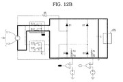
- FIGS. 12A and 12B illustrate the current flow at the time of applying a DC power supply having a normal polarity to the DC power supply apparatus in accordance with the other embodiment of the present disclosure.
- FIGS. 13A and 13B illustrate an output signal graph of a comparison unit at the time applying a DC power supply having a normal polarity to the DC power supply apparatus in accordance with the other embodiment of the present disclosure, and a graph showing a voltage of an input DC power and a voltage of a DC link at the time of applying a DC power supply having a normal polarity to the DC power supply apparatus in accordance with the other embodiment of the present disclosure.
- FIGS. 14A and 14B illustrate the current flow at the time of applying a DC power having an abnormal polarity to the DC power supply apparatus in accordance with the other embodiment of the present disclosure.
- FIGS. 15A and 15B illustrate an output signal graph of a comparison unit at the time of applying a DC power supply having an abnormal polarity to the DC power supply apparatus in accordance with the other embodiment of the present disclosure, and a graph showing a voltage of an input DC power supply and a voltage of a DC link at the time of applying a DC power having an abnormal polarity to the DC power supply apparatus in accordance with the other embodiment of the present disclosure.
- FIGS. 16A to 19B illustrate a power loss graph of a washing machine applied with the DC power supply apparatus in accordance with the other embodiment of the present disclosure and a power loss graph of a washing machine applied with a conventional DC power supply apparatus.
- FIG. 1 is a block diagram illustrating a DC power supply apparatus in accordance with one embodiment of the present disclosure.
- the DC power supply apparatus configured to supply a DC power to a load 170 includes an input unit 110 , a polarity correction unit 120 , a DC link unit 130 , a detection unit 140 , a control unit 150 , and a switch unit 160 .
- the DC power supply apparatus may further include a resistor configured to prevent an excess current from flowing at the polarity correction unit 120 and the DC link unit 130 .
- the input unit 110 is connected to DC power source terminals of outside to receive a DC power of outside, and conveys the DC power input to the load 170 .
- Such an input unit 110 includes a first terminal 111 and a second terminal 112 that are connected to a positive (+) terminal among the DC power source terminals of outside, at which a positive (+) voltage is input, and a negative ( ⁇ ) terminal among the DC power source terminals of outside, at which a negative ( ⁇ ) voltage is input.
- each of the first terminal 111 and the second terminal 112 is provided with a predetermined polarity of the DC power that is to be entered.
- the load 170 is provided with two terminals into which DC power is input, and each of the two terminals is also provided with a predetermined polarity of the DC power.
- the first terminal 111 and the positive (+) terminal of the load 170 are connected to each other, and the second terminal 112 and the negative ( ⁇ ) terminal of the load 170 are connected to each other.
- the DC powers of polarities opposite to the polarities established for the two terminals are applied to the two terminals, and the load 170 either stops operation or breaks down as a result.
- the DC power supply apparatus in order to prevent the breakdown of the load 170 and to facilitate a normal operation, is needed to correct the polarity of the DC power that flows from the input unit 110 to the load 170 .
- the polarity correction unit 120 is connected to the input unit 110 and the switch unit 160 in a parallel manner between the input unit 110 and the switch unit 160 , and when the outside DC power is input to the polarity correction unit 120 through the input unit 110 , the polarity correction unit 120 corrects the polarity of the DC power, and supplies the DC power having the polarity corrected to the load 170 .
- Such a polarity correction unit 120 when a certain time is expired after the DC power of outside is input thereto, forms an open circuit between the input unit 110 and the load 170 . Through such, the flow of a current through the polarity correction unit 120 is cut off.
- Such cutoff occurs as the flow of a current is changed from flowing through the polarity correction unit 120 to flowing through the switch unit 160 .
- the polarity correction unit 120 includes a first polarity correction unit 121 , and a second polarity correction unit 122 .
- the first polarity correction unit 121 may be configured to maintain the respective polarities of the first terminal 111 and the second terminal 112 in a case when the polarity of the first terminal 111 and the polarity of the second terminal 112 are normally connected.
- the second polarity correction unit 122 is configured to correct the polarities of the first terminal 111 and the second terminal 112 in a case when the polarity of the first terminal 111 and the polarity of the second terminal 112 are abnormally connected.
- the first polarity correction unit 121 in a case when the polarities are normally connected, forms a first current path between the input unit 110 and the load 170
- the second polarity correction unit 122 in a case when the polarities are abnormally connected, forms a second current path between the input unit 110 and the load 170 .
- Such a polarity correction unit 120 includes a plurality of diodes (from D 1 to D 4 ). Such a plurality of diodes is formed with a bridge diode.
- the DC link unit 130 is supplied with the DC power through the polarity correction unit 120 or the switch unit 160 .
- the DC link unit after smoothing the supplied DC power, conveys the DC power that is smoothed to the load 170 .
- the DC link unit 130 includes a capacitor C.
- the capacitor C is connected to the input unit 110 and the load 170 in a parallel manner between the input unit 110 and the load 170 .
- the detection unit 140 detects the current flow of the polarity correction unit 120 . By detecting the current flow of the polarity correction unit 120 , it may be determined whether the polarity connection of the first terminal 111 and the second terminal 112 of the input unit 110 is normal or abnormal.
- the detection unit 140 includes a first polarity detection unit 141 connected to the first polarity correction unit 121 and a second polarity detection unit 142 connected to the second polarity detection unit 122 .
- the first polarity detection unit 141 includes a plurality of resistors R 1 and R 2 each connected in parallel to both ends of the first polarity correction unit 121
- the second polarity detection unit 142 includes a plurality of resistors R 3 and R 4 each connected in parallel to both ends of the second polarity correction unit 122 .
- the first polarity detection unit 141 detects the distribution voltage between the both ends of the first polarity correction unit 121
- the second polarity detection unit 142 detects the distribution voltage between the both ends of the second polarity correction unit 122 .
- the first detection unit 141 when a current flows at the first polarity correction unit 121 , detects the distribution voltage that corresponds to the voltage at both ends of the diode of the first polarity correction unit 121 .
- the first detection unit 141 when a current does not flow at the first polarity correction unit 121 , detects the distribution voltage that corresponds to the voltage at both ends of the input unit 110 as the diode of the first polarity correction unit 121 is open.
- the second detection unit 142 when a current flows at the second polarity correction unit 122 , detects the distribution voltage that corresponds to the voltage at both ends of the diode of the second polarity correction unit 122 .
- the second detection unit 142 when a current does not flow at the second polarity correction unit 122 , detects the distribution voltage that corresponds to the voltage at both ends of the input unit 110 as the diode of the second polarity correction unit 122 is open.
- the first polarity detection unit 141 further includes a first comparison unit Com 1
- the second polarity detection unit 142 further includes a second comparison unit Com 2 .
- the first comparison unit Com 1 of the first polarity detection unit 141 compares the distribution voltage detected with a first reference voltage Vr 1 , and outputs a high signal as a detected signal when the distribution voltage is above the first reference voltage, and outputs a low signal as a detected signal when the distribution voltage is below the first reference voltage.
- the second comparison unit Com 2 of the second polarity detection unit 142 compares the distribution voltage detected with a second reference voltage Vr 2 , and outputs a high signal as a detected signal when the distribution voltage is above the second reference voltage, and outputs a low signal as a detected signal when the distribution voltage is below the second reference voltage.
- the first polarity detection unit 141 since the distribution voltage that corresponds to the voltage between the both ends of the diode is detected in a case when a current flows through the first polarity correction unit 121 , outputs a low signal.
- the first polarity detection unit 141 since the distribution voltage that corresponds to the voltage between the both ends of the input unit 110 is detected in a case when a current flows through the second polarity correction unit 122 , outputs a high signal.
- the second polarity detection unit 142 since the distribution voltage that corresponds to the voltage between the both ends of the diode is detected in a case when a current flows through the second polarity correction unit 122 , outputs a low signal.
- the second polarity detection unit 142 since the distribution voltage that corresponds to the voltage between the both ends of the input unit 110 is detected in a case when a current flows through the first polarity correction unit 121 , outputs a high signal.
- the first polarity detection unit 141 and the second polarity detection unit 142 detect at which one of the first current path formed by the current flow of the first polarity correction unit 121 and the second current path formed by the current flow of the second polarity correction unit 122 the DC current flows.
- the control unit 150 determines that the first current path is formed, if the low signal is input from the first polarity detection unit 141 , and controls a first switch unit 161 at the ON position.
- the control unit 150 determines that the second current path is formed when the low signal is input from the second polarity detection unit 142 , and controls a second switch unit 162 at the ON position.
- the control unit 150 when the high signal is input from the second polarity detection unit 142 , may control the first switch unit 161 at the ON position, and when the high signal is input from the first polarity detection unit 141 , may control the second switch unit 162 at the ON position.
- the current path of the DC power flowing from the input unit 110 to the load 170 through the polarity detection unit 140 is hereby changed so that the current path of the DC power supply flows from the input unit 110 to the load 170 through the switch unit 160 .
- the DC power supply apparatus as above when being supplied with the DC power through the DC power source terminal of outside, is supplied through the polarity correction unit 120 at first, but after a certain time is expired, is supplied with the DC power through the switch unit 160 .
- the switch unit 160 is connected in parallel to the polarity correction unit 120 .
- the switch unit 160 includes the first switch unit 161 and the second switch unit 162 .
- the first switch unit 161 in a case when the polarity of the first terminal 111 and the polarity of the second terminal 112 are normally connected, is configured to maintain the respective polarities
- the second switch unit 162 in a case when the polarity of the first terminal 111 and the polarity of the second terminal 112 are abnormally connected, is configured to correct the polarities.
- the first switch unit 161 in a case when the polarities are normally connected, reforms the first current path between the input unit 110 and the load 170 .
- the second switch unit 162 in a case when the polarities are abnormally connected, reforms the second current path between the input unit 110 and the load 170 .
- the first switch unit 161 and the second switch unit 162 operate at the ON or OFF position according to the command of the control unit 150 . At this time, the current path changes from flowing through the polarity correction unit 120 to flowing through the switch unit 160 that is operated at the ON position.
- the switch unit 160 includes a plurality of switches.
- the switch includes a semiconductor switch or a relay.
- the switch unit 160 may be integrally formed with the polarity correction unit 120 .
- one metal oxide-semiconductor field-effect transistor is formed with one switch and one diode connected in parallel to the one switch, and as the MOSFET is provided in plurality, a plurality of switch units and polarity correction units are formed.
- the switch unit 160 and the polarity correction unit 120 are formed with the plurality of MOSFETs.
- FIG. 2 is a circuit diagram illustrating the DC power supply apparatus in accordance with the embodiment of the present disclosure.
- the DC power supply apparatus includes the input unit 110 connected to the DC power source terminals of outside.
- the input unit 110 includes the first terminal 111 connected to the voltage terminal having a positive (+) polarity among the DC power source terminals of outside, and the second terminal 112 connected to the voltage terminal having a negative ( ⁇ ) polarity among the DC power source terminals of outside.
- the input unit 110 is supplied with a DC power of outside Vin through the first terminal 111 and the second terminal 112 .
- the DC power supply apparatus includes the first switch unit 161 and the first polarity correction unit 121 that are configured to form the first current path between the input unit 110 and the load 170 , and the second switch unit 162 and the second polarity correction unit 122 that are configured to form the second current path between the input unit 110 and the load 170 .
- the first switch unit 161 and the first polarity correction unit 121 include a first MOSFET SW 1 and D 1 and a third MOSFET SW 3 and D 3 .
- the second switch unit 162 and the second polarity correction unit 122 include a second MOSFET SW 2 and D 2 and a fourth MOSFET SW 4 and D 4 .
- the first MOSFET includes a first switch SW 1 provided with a source thereof connected to the first terminal 111 of the input unit 110 and with a drain thereof connected to the load 170 , and a first diode D 1 connected in parallel to the source and the drain of the first switch SW 1 .
- an anode of the first diode D 1 is connected to the source of the first switch SW 1 , and a cathode of the first diode D 1 is connected to the drain of the first switch SW 1 .
- the second MOSFET includes a second switch SW 2 provided with a drain thereof connected between the drain of the first MOSFET and the load 170 and with a source thereof connected to the second terminal 112 , and a second diode D 2 connected in parallel to the source and the drain of the second switch SW 2 .
- an anode of the second diode D 2 is connected to the source of the second switch SW 2 , and a cathode of the second diode D 2 is connected to the drain of the second switch SW 2 .
- the third MOSFET includes a third switch SW 3 provided with a drain thereof connected to the source of the second switch SW 2 and to the second terminal 112 of the input unit 110 and with a source thereof connected to a ground, and a third diode D 3 connected in parallel to the source and the drain of the third switch SW 3 .
- an anode of the third diode D 3 is connected to the source of the third switch SW 3 , and a cathode of the third diode D 3 is connected to the drain of the third switch SW 3 .
- the fourth MOSFET includes a fourth switch SW 4 provided with a drain thereof connected to the source of the first switch SW 1 and to the first terminal 111 of the input unit 110 and with a source thereof connected to a ground, and a fourth diode D 4 connected in parallel to the source and the drain of the fourth switch SW 4 .
- an anode of the fourth diode D 4 is connected to the source of the fourth switch SW 4 , and a cathode of the fourth diode D 4 is connected to the drain of the fourth switch SW 4 .
- the diodes from the first diode to the fourth diode are the body diodes of the first switch to the fourth switch.
- Each gate of the plurality of the MOSFETs is connected to the control unit 150 , and is input with an ON/OFF command from the control unit 150 .
- the DC power supply apparatus includes a capacitor C connected between the drains of the first switch SW 1 and the second switch SW 2 , and the sources of the third switch SW 3 and the fourth switch SW 4 .
- the capacitor C is connected in parallel between the plurality of MOSFETs and the load.
- the load 170 is connected in parallel to the both ends of the capacitor C.
- the DC power supply apparatus further includes the first polarity detection unit 141 connected to the first polarity correction unit 161 and the second polarity detection unit 142 connected to the second polarity correction unit 162 .
- the first polarity detection unit 141 includes a first voltage distribution unit R 1 and R 2 connected in parallel to the both ends of the third diode D 3 , which is provided at the third MOSFET of the first switch unit 161 , and the first comparison unit com 1 connected between the first resistor R 1 and the second resistor R 2 , both of which correspond to the first voltage distribution unit.
- the cathode of the third diode D 3 is connected to the first resistor that corresponds to the first voltage distribution unit, and also, the second terminal 122 is connected to the first resistor.
- the anode of the third diode D 3 is connected to the second resistor, and also the ground is connected to the second resistor.
- the first comparison unit com 1 is input with the first distribution voltage from the first distribution resistor therein through the positive (+) terminal, and is input with the first reference voltage Vr 1 therein through the negative ( ⁇ ) terminal.
- the first comparison unit com 1 compares the first distribution voltage with the first reference voltage, and in a case when the first distribution voltage is above the first reference voltage, the first comparison unit com 1 outputs a high signal, and in a case when the first distribution voltage is below the first reference voltage, the first comparison unit com 1 outputs a low signal.
- the first comparison unit com 1 outputs the high signal or the low signal, both of which are the detection signals, to the control unit 150 .
- the second polarity detection unit 142 includes a second voltage distribution unit R 3 and R 4 connected in parallel to the both ends of the fourth diode D 4 , which is provided at the fourth MOSFET of the second switch unit 162 , and the second comparison unit com 2 connected between the third resistor R 3 and the fourth resistor R 4 , both of which correspond to the second voltage distribution unit.
- the cathode of the fourth diode D 4 is connected to the third resistor of the second voltage distribution unit, and also the first terminal 121 is connected to the third resistor.
- the anode of the fourth diode D 4 is connected to the fourth resistor, and also the ground is connected to the fourth resistor.
- the second comparison unit com 2 is input with the second distribution voltage from the second distribution resistor therein through the positive (+) terminal, and is input with the second reference voltage Vr 2 therein through the negative ( ⁇ ) terminal.
- the second comparison unit com 2 compares the second distribution voltage with the second reference voltage, and in a case when the second distribution voltage is above the second reference voltage, the second comparison unit com 2 outputs a high signal, and in a case when the second distribution voltage is below the second reference voltage, the second comparison unit com 1 outputs a low signal.
- the second comparison unit com 2 outputs the high signal or the low signal, both of which are the detection signals, to the control unit 150 .
- the control unit 150 by using the signal that is output from the first comparison unit com 1 and the second comparison unit com 2 , may determine the polarity connected to at least one of the first terminal and the second terminal of the input unit 110 .
- control unit 150 in a case when a low signal is output from the first comparison unit, may determine that the voltage terminal having a positive (+) polarity is connected to the first terminal.
- the control unit 150 in a case when a low signal is output from the second comparison unit, may determine that the voltage terminal having a negative ( ⁇ ) polarity is connected to the second terminal.
- FIGS. 3A and 3B illustrate the current flow at the time of applying a DC power having a normal polarity to the DC power supply apparatus in accordance with the embodiment of the present disclosure.
- the DC power supply apparatus when each of the first terminal 111 and the second terminal 112 of the DC power supply apparatus is normally connected to the established polarity by having the first terminal 111 and the second terminal 112 of the DC power supply apparatus connected to the positive (+) voltage terminal of and the negative ( ⁇ ) voltage terminal of the DC power source terminal of outside, the DC power supply apparatus is input with the positive (+) polarity voltage through the first terminal 111 , and is input with the negative ( ⁇ ) polarity voltage through the second terminal 112 .
- the DC power supply apparatus through the firth terminal 111 and the second terminal 112 , is input with the DC power supply Vin of outside. At this time, the current flow is formed from the first terminal 111 to the second terminal 112 .
- the current flows to the first diode D 1 of the MOSFET connected to the first terminal 111 , and the current passed through the first diode D 1 flows to the third diode D 3 of the third MOSFET through the load 170 and the capacitor C, and then flows to the second terminal 112 .
- the first current path is formed, and the polarity of the DC power supply normally connected between the DC power source terminal of outside and the DC power supply apparatus may be maintained.
- the polarity correction unit at which the current flow is formed is detected through the first polarity detection unit and the second polarity detection unit.
- the first polarity detection unit 141 detects the first distribution voltage between the first resistor R 1 and the second resistor R 2
- the second polarity detection unit 142 detects the second distribution voltage between the third resistor R 3 and the fourth resistor R 4 .
- the distribution voltage detected is less than the first reference voltage, and since the distribution voltage corresponding to the voltage between the first terminal 111 and the ground is detected at the second polarity detection unit 142 , the distribution voltage detected is more than the second reference voltage.
- a low signal is output through the first comparison unit com 1 of the first polarity detection unit 141 and a high signal is output through the second comparison unit com 2 of the second polarity detection unit 142 .
- the control unit 150 is input with the detection signals from the first comparison unit com 1 and the second comparison unit com 2 , confirms the comparison unit that has transmitted a low signal, and controls the switch of the switch unit corresponding to the confirmed comparison unit at the ON position.
- the control unit 150 controls the first switch SW 1 of the first MOSFET and the third switch SW 3 of the third MOSFET of the first switch unit 161 at the ON position.
- the information of the first switch unit 161 corresponding to the first comparison unit com 1 and the information of the second switch unit 162 corresponding to the second comparison unit com 2 are pre-stored.
- control unit 150 may be input with the detection signals from the first comparison unit com 1 and the comparison unit, and confirm the comparison unit that has transmitted a high signal, and control the switch of the switch unit corresponding to the confirmed comparison unit at the ON position.
- the information of the second switch unit 162 corresponding to the first comparison unit com 1 and the information of the first switch unit 161 corresponding to the second comparison unit com 2 may be pre-stored.
- the first switch SW 1 and the third switch SW 3 are operated at the ON position.
- the current of the DC power supply apparatus flows to the first switch SW 1 of the first MOSFET connected to the first terminal 111 , and the current passed through the first switch SW 1 flows to the second terminal 112 after flowing to the third switch SW 3 of the third MOSFET through the load 170 and the capacitor C.
- the flow of the current from the first terminal 111 to the second terminal 112 is reformed as a result.
- FIG. 4A an output signal graph of a comparison unit at the time of applying a DC power having a normal polarity to the DC power supply apparatus in accordance with the embodiment of the present disclosure is illustrated
- FIG. 4B a graph showing a voltage of an input DC power and a voltage of a DC link at the time of applying a DC power having a normal polarity to the DC power supply apparatus in accordance with the embodiment of the present disclosure is illustrated.
- a low signal is output from the output (MG: Minus Gate) of the first comparison unit, and a high signal is output from the output (PG: Plus Gate) of the second comparison unit
- a high signal is input into the gate (PG: Plus Gate) of the first switch SW 1 of the first MOSFET and the gate (PG: Plus Gate) of the third switch SW 3 of the third MOSFET, the first switch and the third switch being operated when a positive (+) voltage is applied
- a low signal is input into the gate (MG: Minus Gate) of the second switch SW 2 of the second MOSFET and the gate (MG: Minus Gate) of the fourth switch SW 4 of the fourth MOSFET, the second switch and the fourth switch being operated when a negative ( ⁇ ) voltage is applied.
- the voltage Vin of the DC power is at about 380V, and the voltage Vc of the DC link which is the voltage of both ends of the capacitor C is about 379.4V. That is, the DC power supply apparatus is found to have less loss of power.
- FIGS. 5A and 5B illustrate the current flow at the time of applying a DC power having an abnormal polarity to the DC power supply apparatus in accordance with the embodiment of the present disclosure is illustrated.
- the DC power supply apparatus is input with the positive (+) voltage through the first terminal 111 and is input with the negative ( ⁇ ) voltage through the second terminal 112 .
- the DC power supply apparatus through the first terminal 111 and the second terminal 112 , is input with the DC power supply Vin of outside. At this time, a current flow from the second terminal 112 to the first terminal 111 is formed.
- the current flows to the second diode D 1 of the second MOSFET connected to the second terminal 112 , and the current passed through the second diode D 2 flows to the fourth diode D 4 of the fourth MOSFET through the load 170 and the capacitor C, and then flows to the first terminal 111 . Accordingly, the second current path is formed, and the polarity of the DC power supply abnormally connected between the DC power source terminal of outside and the DC power supply apparatus may be corrected.
- the polarity correction unit at which the current flow is formed is detected through the first polarity detection unit and the second polarity detection unit.
- the first polarity detection unit 141 detects the first distribution voltage between the first resistor R 1 and the second resistor R 2
- the second polarity detection unit 142 detects the second distribution voltage between the third resistor R 3 and the fourth resistor R 4 .
- the distribution voltage detected is more than the first reference voltage, and since the distribution voltage corresponding to the voltage of the both ends of the fourth diode D 4 is detected at the second polarity detection unit 142 , the distribution voltage detected is less than the first reference voltage.
- a high signal is output through the first comparison unit com 1 of the first polarity detection unit 141 and a low signal is output through the second comparison unit com 2 of the second polarity detection unit 142 .
- the control unit 150 is input with the detection signals from the first comparison unit com 1 and the second comparison unit com 2 , confirms the comparison unit that has transmitted a low signal, and controls the switch of the switch unit corresponding to the confirmed comparison unit at ON position.
- control unit 150 controls the second switch SW 2 of the second MOSFET and the fourth switch SW 4 of the fourth MOSFET at ON position
- the current of the DC power supply apparatus flows to the second switch SW 2 of the second MOSFET connected to the second terminal 112 , and the current passed through the second switch SW 2 flows to the first terminal 111 after flowing to the fourth switch SW 4 of the fourth MOSFET through the load 170 and the capacitor C.
- FIG. 6A an output signal graph of a comparison unit at the time of applying a DC power supply having an abnormal polarity to the DC power supply apparatus in accordance with the embodiment of the present disclosure is illustrated
- FIG. 6B a graph showing a voltage of an input DC power and a voltage of a DC link at the time of applying a DC power having an abnormal polarity to the DC power supply apparatus in accordance with the embodiment of the present disclosure is illustrated.
- a high signal is output from the output (MG: Minus Gate) of the first comparison unit and a low signal is output from the output (Plus Gate) of the second comparison unit
- a high signal is input into the gate (MG: Minus Gate) of the second switch SW 2 of the second MOSFET and the gate (MG: Minus Gate) of the fourth switch SW 4 of the fourth MOSFET, the second switch and the fourth switch being operated when a negative ( ⁇ ) voltage is applied
- a low signal is input into the gate (PG: Plus Gate) of the first switch SW 1 of the first MOSFET and the gate (PG: Plus Gate) of the third switch SW 3 of the third MOSFET, the first switch and the third switch being operated when a positive (+) voltage is applied.
- the voltage Vin of the DC power is at about ⁇ 380V
- the voltage Vc of the DC link which is the voltage of the both ends of the capacitor C is about 380V. That is, the DC power supply apparatus is found to have less loss of power. In addition, it is found that the polarity of the DC power supply entered thereto is being corrected.
- the DC power supply apparatus of the present disclosure corrects the polarity of the DC power supply by using the body diode of the MOSFET, and then, by turning on the MOSFET changes the current path, changes the current path from flowing through the diode having greater loss factor to flowing through the MOSFET.
- the embodiment since the correction of the polarity of the DC power supply apparatus is implemented by only using the MOSFET without using a separate bridge diode, the embodiment may be done easily.
- FIGS. 7A to 10B each illustrate a graph of the power loss of a washing machine applied with the DC power supply apparatus in accordance with the embodiment of the present disclosure and a graph of the power loss of a washing machine applied with a conventional DC power supply apparatus.
- FIGS. 7A , 8 A, 9 A and 10 A are graphs of power loss of a conventional DC power supply apparatus using a bridge diode
- FIGS. 7B , 8 B, 9 B and 10 B are graphs of power loss of a DC power supply apparatus of the embodiment of the present disclosure.
- FIGS. 7A and 7B illustrate the power loss graphs at a standby cycle, and the power loss of a conventional drum washing machine is about 1.73 W, and the power loss of the embodiment of the present disclosure is at about 0.05 W.
- FIGS. 8A and 8B illustrate the power loss graphs at a washing cycle, and the power loss of a conventional drum washing machine is about 19.0 W, and the power loss of the embodiment of the present disclosure is at about 6.09 W.
- FIGS. 9A and 9B illustrate the power loss graphs at a hot water supply cycle, and the power loss of a conventional drum washing machine is about 25.7 W, and the power loss of the embodiment of the present disclosure is at about 11.12 W.
- FIGS. 10A and 10B illustrate the power loss graph at a drying cycle, and the power loss of a conventional drum washing machine is about 42.2 W, and the power loss of the embodiment of the present disclosure is at about 18.84 W.
- FIG. 11 is a circuit diagram of a DC power supply apparatus in accordance with another embodiment of the present disclosure, and the DC power supply apparatus including the switch unit 160 formed with the relay therein and the polarity correction unit 120 formed with the diode will be used as examples for explanation.
- the DC power supply apparatus includes the input unit 110 connected to the DC power source terminal of outside.
- the input unit 110 includes the first terminal 111 connected to the voltage terminal having a positive (+) polarity among the DC power source terminals of outside, and the second terminal 112 connected to the voltage terminal having a negative ( ⁇ ) polarity.
- the input unit 110 is supplied with a DC power of outside Vin through the first terminal 111 and the second terminal 112 .
- the DC power supply apparatus includes the first switch unit 161 and the first polarity correction unit 121 , which are configured to form the first current path between the input unit 110 and the load 170 , and the second switch unit 162 and the second polarity correction unit 122 , which are configured to form the second current path between the input unit 110 and the load 170 .
- the first switch unit 161 includes a first relay S 11 and a second relay S 12
- the second switch unit 162 includes a third relay S 21 and a fourth relay S 22 .
- a first contact point of the first relay S 11 is connected to the first terminal 111 , a second contact point of the first relay S 11 is connected to the load 170 , a first contact point of the second relay S 12 is connected to the second terminal 112 , and a second contact point of the second relay S 12 is connected to the ground.
- first contact point and the second contact point of the first relay S 11 and the second relay S 12 are electrically connected by an armature.
- the armature moves according to the command of the control unit 150 . That is, when a current is applied to a coil according to the command of the control unit 150 , the coil changes into an electromagnet, and the armature is moved by the electromagnet to connect the first contact point and the second contact point.
- a first contact point of the third relay S 21 is connected to the first terminal 111 , a second contact point of the third relay S 21 is connected to the load 170 , a first contact point of the fourth relay S 22 is connected to the second terminal 112 , and a second contact point of the fourth relay S 22 is connected to the ground.
- the first contact point of the third relay S 21 and the second contact point of the fourth relay S 22 are also electrically connected by the armature.
- the first polarity correction unit 121 includes a first diode D 1 and a third diode D 3
- the second polarity correction unit 121 includes a second diode D 2 and a fourth diode D 4 .
- the diodes from first diode to the fourth diode form a bridge diode.
- a cathode of the first diode D 1 is connected to the second contact point of the first relay S 11 and to the second contact point of the fourth relay S 22 , and an anode of the first diode D 1 is connected to the first terminal 111 .
- the anode of the first diode D 1 is connected to the first terminal 111 through a resistor R 5 .
- the resistor R 5 prevents the excess current from applied at the diode and the capacitor.
- the resistor R 5 limits the inrush current that flows at the capacitor first.
- the resistor R 5 if the inrush current is higher than the rated current of the diode, prevents the diode from being damaged from overheating.
- a cathode of the second diode D 2 is connected to the second contact point of the first relay S 11 and to the second contact point of the fourth relay S 22 , and also the cathode source is connected to the anode of the first diode D 1 .
- an anode of the second diode D 2 is connected to the second terminal 112 .
- a cathode of the third diode D 3 is connected to the second terminal 112 , and also the cathode of the third diode D 3 is connected to the anode of the second diode D 2 .
- An anode of the third diode D 3 is connected to the ground, and also is connected to the second contact point of the second relay S 12 and to the second contact point of the third relay S 21 .
- a cathode of the fourth diode D 4 is connected to the first terminal 111 through the resistor R 5 , and also is connected to the anode of the first diode D 1 .
- An anode source of the fourth diode D 4 is connected to the ground, and also is connected to the second contact point of the second relay S 12 and to the second contact point of the third relay S 21 .
- the capacitor C is connected in parallel between the bridge diode D 1 to D 4 and the load 170 .
- the load 170 is connected in parallel to the both ends of the capacitor C.
- the DC power supply apparatus further includes the first polarity detection unit 141 connected to the first polarity correction unit 161 , and the second polarity detection unit 142 connected to the second polarity correction unit 162 .
- the first polarity detection unit 141 includes the first voltage distribution unit R 1 and R 2 connected in parallel to the both ends of the third diode D 3 , and the first comparison unit com 1 connected between the first resistor R 1 and the second resistor R 2 both of which are of the first voltage distribution unit.
- the cathode of the third diode D 3 is connected to one side of the first distribution resistor, and the second terminal 122 also is connected to the one side of the first distribution resistor.
- the anode of the third diode D 3 is connected to the other side of the first distribution resistor and the ground is also connected to the other side of the first resistor.
- the first comparison unit com 1 is input with the first distribution voltage from the first distribution resistor through a positive (+) terminal, and is input with the first reference voltage Vr 1 through a negative ( ⁇ ) terminal.
- the first comparison unit com 1 compares the first distribution voltage with the first reference voltage, and when the first distribution voltage is above the first reference voltage, outputs a high signal, and when the first distribution voltage is below the first reference voltage, outputs a low signal.
- the first comparison unit com 1 outputs the high signal or the low signal, both of which are the detection signals, to the control unit 150 .
- the second polarity detection unit 142 includes a second voltage distribution unit R 3 and R 4 connected in parallel to the both ends of the fourth diode D 4 , and the second comparison unit com 2 connected between the third resistor R 3 and the fourth resistor R 4 , both of which are of the second voltage distribution unit.
- the cathode of the fourth diode D 4 is connected to one side of the second distribution resistor, and the first terminal 121 is also connected to the one side of the second distribution resistor.
- the anode of the fourth diode D 4 is connected to the other side of the second distribution resistor and the ground is also connected to the other side of the second distribution resistor.
- the second comparison unit com 2 is input with the second distribution voltage from the second distribution resistor through the positive (+) source, and is input with the second reference voltage Vr 2 therein through the negative ( ⁇ ) terminal.
- the second comparison unit com 2 compares the second distribution voltage with the second reference voltage, and in a case when the second distribution voltage is above the second reference voltage, the second comparison unit com 2 outputs a high signal, and in a case when the second distribution voltage is below the second reference voltage, the second comparison unit com 1 outputs a low signal.
- the second comparison unit com 2 outputs the high signal or the low signal, both of which are the detection signals, to the control unit 150 .
- the control unit 150 controls the current applied to the coils of the plurality of the relays S 11 , S 12 , S 21 , and S 22 .
- FIGS. 12A and 12B illustrate the current flow at the time of applying a DC power supply having a normal polarity to the DC power supply apparatus in accordance with the other embodiment of the present disclosure.
- the DC power supply apparatus is input with the voltage having a positive (+) polarity through the first terminal 111 , and is input with the voltage having a negative ( ⁇ ) polarity through the second terminal 112 .
- the DC power supply apparatus through the firth terminal 111 and the second terminal 112 , is input with the DC power Vin of outside. At this time, the current flow is formed from the first terminal 111 to the second terminal 112 .
- the current flows to the first diode D 1 through the resistor R 5 connected to the first terminal 111 , and the current passed through the first diode D 1 flows to the third diode D 3 through the load 170 and the capacitor C, and then flows to the second terminal 112 .
- the first current path is formed, and the polarity of the DC power supply normally connected between the DC power source terminal of outside and the DC power supply apparatus may be maintained.
- the polarity correction unit at which the current flow is formed is detected through the first polarity detection unit 141 and the second polarity detection unit 142 .
- the first polarity detection unit 141 detects the first distribution voltage between the first resistor R 1 and the second resistor R 2
- the second polarity detection unit 142 detects the second distribution voltage between the third resistor R 3 and the fourth resistor R 4 .
- the distribution voltage detected is less than the first reference voltage, and since the distribution voltage corresponding to the voltage between the first terminal 111 and the ground is detected at the second polarity detection unit 142 , the distribution voltage detected is more than the second reference voltage.
- a low signal is output through the first comparison unit com 1 of the first polarity detection unit 141 and a high signal is output through the second comparison unit com 2 of the second polarity detection unit 142 .
- the control unit 150 is input with the detection signals from the first comparison unit com 1 and the second comparison unit com 2 , confirms the comparison unit that has transmitted a low signal, and controls the switch of the switch unit corresponding to the confirmed comparison unit at the ON position.
- the control unit 150 controls the first relay S 11 and the second relay S 12 of the first switch unit 161 at the ON position.
- the information of the first switch unit 161 corresponding to the first comparison unit com 1 and the information of the second switch unit 162 corresponding to the second comparison unit com 2 are pre-stored.
- control unit 150 may input with the detection signals from the first comparison unit com 1 and the second comparison unit com 2 , confirm the comparison unit that has transmitted a high signal, and control the switch of the switch unit corresponding to the confirmed comparison unit at the ON position.
- the information of the second switch unit 162 corresponding to the first comparison unit com 1 and the information of the first switch unit 161 corresponding to the second comparison unit com 2 may be pre-stored.
- the first relay S 11 and the second relay S 12 of the first switch unit 161 of the DC power supply apparatus As illustrated on FIG. 12B , as a high signal is input into the first relay S 11 and at the second relay S 12 of the first switch unit 161 of the DC power supply apparatus and a low signal is input into the third relay S 21 and at the fourth relay S 22 of the DC power supply apparatus, the first relay S 11 and the second relay S 12 are operated at the ON position and the third relay S 21 and the fourth relay S 22 are operated at the OFF position.
- the current of the DC power supply apparatus flows to the first relay S 11 connected to the first terminal 111 , and the current passed through the first relay S 11 flows to the second terminal 112 after flowing to the second relay S 12 through the load 170 and the capacitor C.
- the flow of the current from the first terminal 111 to the second terminal 112 is reformed as a result.
- FIG. 13A an output signal graph of a comparison unit at the time applying a DC power supply having a normal polarity to the DC power supply apparatus in accordance with the other embodiment of the present disclosure.
- FIG. 13B a graph showing a voltage of an input DC power and a voltage of a DC link at the time of applying a DC power supply having a normal polarity to the DC power supply apparatus in accordance with the other embodiment of the present disclosure is illustrated.
- a current is applied to the coils of the first relay S 11 and the second relay S 12 , both of which are operated at the time of the positive (+) voltage is applied, while a current is not applied to the coils of the third relay S 21 and the fourth relay S 22 , both of which are operated at the time of the negative ( ⁇ ) voltage is applied.
- the voltage Vin of the DC power supply is at about 380V, and the voltage Vc of the DC link which is the voltage of both ends of the capacitor C is about 379.4V. That is, the DC power supply apparatus is found to have less loss of power.
- FIGS. 14A and 14B illustrate the current flow at the time of applying a DC power having an abnormal polarity to the DC power supply apparatus in accordance with the other embodiment of the present disclosure.
- the DC power supply apparatus through the first terminal 111 and the second terminal 112 , is input with the DC power supply Vin of outside. At this time, a current flow from the second terminal 112 to the first terminal 111 is formed.
- the current flows to the second diode D 1 connected to the second terminal 112 , and the current passed through the second diode D 2 flows to the fourth diode D 4 through the load 170 and the capacitor C, and then flows to the first terminal 111 through the fifth resistor R 5 .
- the second current path is formed, and the polarity of the DC power supply abnormally connected between the DC power source terminal of outside and the DC power supply apparatus may be corrected.
- the relays from the first relay to the fourth relay are at OFF position, and a current does not flow therethrough.
- the polarity correction unit at which the current flow is formed is detected through the first polarity detection unit and the second polarity detection unit.
- the first polarity detection unit 141 detects the first distribution voltage between the first resistor R 1 and the second resistor R 2
- the second polarity detection unit 142 detects the second distribution voltage between the third resistor R 3 and the fourth resistor R 4 .
- the distribution voltage detected is more than the first reference voltage, and since the distribution voltage corresponding to the voltage of the both ends of the fourth diode D 4 is detected at the second polarity detection unit 142 , the distribution voltage detected is less than the first reference voltage.
- a high signal is output through the first comparison unit com 1 of the first polarity detection unit 141 and a low signal is output through the second comparison unit com 2 of the second polarity detection unit 142 .
- the control unit 150 is input with the detection signals from the first comparison unit com 1 and the second comparison unit com 2 , confirms the comparison unit that has transmitted a low signal, and controls the switch of the switch unit corresponding to the confirmed comparison unit at the ON position.
- control unit 150 controls the third relay S 21 and the fourth relay S 22 of the second switch unit 162 at the ON position.
- the third relay S 21 and the fourth relay S 22 are operated at ON position, as the operating signal for the third relay and the fourth relay is transmitted according to the command of the control unit 150 and then the armature is operated when a current flows at the coils of the third relay S 21 and the fourth relay S 22 of the DC power supply apparatus.
- the second current path is changed from flowing through the second diode D 2 and the fourth diode D 4 to flowing through the third relay S 21 and the fourth relay S 22 , both of which are provided with less resistance when compared to the diode D 2 and the diode D 4 .
- the current of the DC power supply apparatus flows to the fourth relay S 22 connected to the second terminal 112 , and the current passed through the fourth relay S 22 flows to the first terminal 111 after flowing to the third relay S 21 through the load 170 and the capacitor C.
- FIG. 15A an output signal graph of a comparison unit at the time of applying a DC power supply having an abnormal polarity to the DC power supply apparatus in accordance with the other embodiment of the present disclosure is illustrated
- FIG. 15B a graph showing a voltage of an input DC power supply and a voltage of a DC link at the time of applying a DC power having an abnormal polarity to the DC power supply apparatus in accordance with the other embodiment of the present disclosure is illustrated.
- a current is not applied to the coil of the first relay S 11 and at the coil of the second relay S 12 , both of which are operated at the time of the positive (+) voltage is applied, while a current is applied to the coil of the third relay S 21 and to the coil of the fourth relay S 22 , both of which are operated at the time of the negative ( ⁇ ) voltage is applied.
- the voltage Vin of the DC power supply is at about ⁇ 380V, and the voltage Vc of the DC link which is the voltage of both ends of the capacitor C is about 380V. That is, the DC power supply apparatus is found to have less loss of power. In addition, it is found that the polarity of the DC power supply entered thereto is corrected.
- the loss factor at the relay is significantly low, as the relay enables a current to flow through the armature, which is nearly same as a lead wire, after the contact point is connected.
- an effect of an initial charging circuit may be attained at the time of the initial correction of the polarity of the DC power supply.
- FIGS. 16A to 19B each illustrate a power loss graph of a washing machine applied with the DC power supply apparatus in accordance with the other embodiment of the present disclosure and a power loss graph of a washing machine applied with a conventional DC power supply apparatus.
- FIGS. 16A , 17 A, 18 a and 19 A are power loss graphs of a conventional DC power supply apparatus using a bridge diode
- FIGS. 16B , 17 B, 18 B and 19 B are power loss graphs of a DC power supply graph of the embodiment of the present disclosure.
- FIGS. 16A and 16B illustrate the power loss graphs at a standby cycle, and the power loss of a conventional drum washing machine is about 1.73 W, and the power loss of the embodiment of the present disclosure is at about 0.03 W.
- FIGS. 17A and 17B illustrate the power loss graphs at a washing cycle, and the power loss of a conventional drum washing machine is about 19.0 W, and the power loss of the embodiment of the present disclosure is at about 3.77 W.
- FIGS. 18A and 18B illustrate the power loss graphs at a hot water supply cycle, and the power loss of a conventional drum washing machine is about 25.7 W, and the power loss of the embodiment of the present disclosure is at about 6.86 W.
- FIGS. 19A and 19B illustrate the power loss graphs at a drying cycle, and the power loss of a conventional drum washing machine is about 42.2 W, and the power loss of the embodiment of the present disclosure is at about 18.4 W.
- the low power loss is provided at the DC power supply apparatus which is configured to correct the polarity by use of the diode and then change the current path by use of the relay in a state when the polarity is corrected, when compared to the DC power supply apparatus which uses only the bridge diode at each operation cycle.
Abstract
Description
Claims (17)
Applications Claiming Priority (2)
| Application Number | Priority Date | Filing Date | Title |
|---|---|---|---|
| KR1020120011427A KR101861728B1 (en) | 2012-02-03 | 2012-02-03 | DC power supply apparatus |
| KR10-2012-0011427 | 2012-02-03 |
Publications (2)
| Publication Number | Publication Date |
|---|---|
| US20130200874A1 US20130200874A1 (en) | 2013-08-08 |
| US9081395B2 true US9081395B2 (en) | 2015-07-14 |
Family
ID=47632908
Family Applications (1)
| Application Number | Title | Priority Date | Filing Date |
|---|---|---|---|
| US13/755,270 Expired - Fee Related US9081395B2 (en) | 2012-02-03 | 2013-01-31 | DC power supply apparatus configured to correct input polarity of DC power |
Country Status (4)
| Country | Link |
|---|---|
| US (1) | US9081395B2 (en) |
| EP (1) | EP2639917B1 (en) |
| KR (1) | KR101861728B1 (en) |
| ES (1) | ES2715350T3 (en) |
Cited By (1)
| Publication number | Priority date | Publication date | Assignee | Title |
|---|---|---|---|---|
| US20170054290A1 (en) * | 2015-08-20 | 2017-02-23 | Fortinet, Inc. | Polarity recognition and swapping for dc powered devices |
Families Citing this family (5)
| Publication number | Priority date | Publication date | Assignee | Title |
|---|---|---|---|---|
| KR20150030078A (en) | 2013-09-11 | 2015-03-19 | 엘에스산전 주식회사 | Photovoltaic inverter |
| SE540397C2 (en) * | 2016-11-25 | 2018-09-11 | Manetos Ab | Electric circuit with low voltage drop |
| CN113260946B (en) * | 2018-12-24 | 2023-03-21 | 浙江大华技术股份有限公司 | Method and system for enabling polarity of data signal to be self-adaptive |
| KR102091616B1 (en) * | 2018-12-28 | 2020-03-20 | 인하대학교 산학협력단 | Protection Circuits for Reversing the Polarity of DC Plug |
| GB2590928B (en) * | 2020-01-07 | 2022-07-06 | Porsche Ag | Charger for electric vehicles |
Citations (10)
| Publication number | Priority date | Publication date | Assignee | Title |
|---|---|---|---|---|
| US5331323A (en) * | 1992-05-11 | 1994-07-19 | Yozan Inc. | Analog-to-digital connecter using multi-gate field effect transistors |
| US5617473A (en) * | 1995-06-23 | 1997-04-01 | Harris Corporation | Sign bit integrator and method |
| US5946205A (en) * | 1996-10-18 | 1999-08-31 | Kabushiki Kaisha Toshiba | Power conversion system with series connected self-commutated converters |
| US20010045853A1 (en) * | 2000-05-26 | 2001-11-29 | Nec Corporation | Timing difference division circuit and signal controlling method and apparatus |
| US6977827B2 (en) * | 2004-03-22 | 2005-12-20 | American Superconductor Corporation | Power system having a phase locked loop with a notch filter |
| US7184282B2 (en) * | 2005-03-11 | 2007-02-27 | Origin Electric Company, Limited | Single-phase power conversion device and three-phase power conversion device |
| US7199528B2 (en) * | 2005-04-21 | 2007-04-03 | Energy Conservation Technologies, Inc. | Control circuit for maintaining constant power in power factor corrected electronic ballasts and power supplies |
| US7638986B2 (en) * | 2006-06-28 | 2009-12-29 | Mitsubishi Electric Corporation | Control system for static VAR compensator |
| US20100156185A1 (en) * | 2008-12-23 | 2010-06-24 | Samsung Electro-Mechanics Co., Ltd. | Photovoltaic and fuel cell hybrid generation system using single converter and single inverter, and method of controlling the same |
| US20130207621A1 (en) * | 2012-02-09 | 2013-08-15 | Minebea Co., Ltd. | Power factor correction circuit |
Family Cites Families (6)
| Publication number | Priority date | Publication date | Assignee | Title |
|---|---|---|---|---|
| US4420786A (en) * | 1981-11-16 | 1983-12-13 | Motorola, Inc. | Polarity guard circuit |
| JP3259611B2 (en) * | 1995-11-08 | 2002-02-25 | 日本電信電話株式会社 | DC power supply system |
| US6181588B1 (en) * | 1998-09-25 | 2001-01-30 | Dell Usa, L.P. | Constant polarity input device including synchronous bridge rectifier |
| WO2008001644A1 (en) * | 2006-06-27 | 2008-01-03 | Panasonic Electric Works Co., Ltd. | Polarity switching circuit and feeding unit |
| WO2011083336A2 (en) * | 2010-01-08 | 2011-07-14 | Holdip Limited | Improvements relating to rectifier circuits |
| TW201214923A (en) * | 2010-09-29 | 2012-04-01 | Fortune Semiconductor Corp | Polarity switch circuit in charger |
-
2012
- 2012-02-03 KR KR1020120011427A patent/KR101861728B1/en active IP Right Grant
-
2013
- 2013-01-31 US US13/755,270 patent/US9081395B2/en not_active Expired - Fee Related
- 2013-02-01 ES ES13153759T patent/ES2715350T3/en active Active
- 2013-02-01 EP EP13153759.9A patent/EP2639917B1/en active Active
Patent Citations (11)
| Publication number | Priority date | Publication date | Assignee | Title |
|---|---|---|---|---|
| US5331323A (en) * | 1992-05-11 | 1994-07-19 | Yozan Inc. | Analog-to-digital connecter using multi-gate field effect transistors |
| US5617473A (en) * | 1995-06-23 | 1997-04-01 | Harris Corporation | Sign bit integrator and method |
| US5946205A (en) * | 1996-10-18 | 1999-08-31 | Kabushiki Kaisha Toshiba | Power conversion system with series connected self-commutated converters |
| US20010045853A1 (en) * | 2000-05-26 | 2001-11-29 | Nec Corporation | Timing difference division circuit and signal controlling method and apparatus |
| US6977827B2 (en) * | 2004-03-22 | 2005-12-20 | American Superconductor Corporation | Power system having a phase locked loop with a notch filter |
| US7184282B2 (en) * | 2005-03-11 | 2007-02-27 | Origin Electric Company, Limited | Single-phase power conversion device and three-phase power conversion device |
| US7199528B2 (en) * | 2005-04-21 | 2007-04-03 | Energy Conservation Technologies, Inc. | Control circuit for maintaining constant power in power factor corrected electronic ballasts and power supplies |
| US7638986B2 (en) * | 2006-06-28 | 2009-12-29 | Mitsubishi Electric Corporation | Control system for static VAR compensator |
| US20100156185A1 (en) * | 2008-12-23 | 2010-06-24 | Samsung Electro-Mechanics Co., Ltd. | Photovoltaic and fuel cell hybrid generation system using single converter and single inverter, and method of controlling the same |
| US8598741B2 (en) * | 2008-12-23 | 2013-12-03 | Samsung Electro-Mechanics Co, Ltd. | Photovoltaic and fuel cell hybrid generation system using single converter and single inverter, and method of controlling the same |
| US20130207621A1 (en) * | 2012-02-09 | 2013-08-15 | Minebea Co., Ltd. | Power factor correction circuit |
Cited By (4)
| Publication number | Priority date | Publication date | Assignee | Title |
|---|---|---|---|---|
| US20170054290A1 (en) * | 2015-08-20 | 2017-02-23 | Fortinet, Inc. | Polarity recognition and swapping for dc powered devices |
| US9917438B2 (en) * | 2015-08-20 | 2018-03-13 | Fortinet, Inc. | Polarity recognition and swapping for DC powered devices |
| US20180191157A1 (en) * | 2015-08-20 | 2018-07-05 | Fortinet, Inc. | Polarity recognition and swapping for dc powered devices |
| US10505365B2 (en) * | 2015-08-20 | 2019-12-10 | Fortinet, Inc. | Polarity recognition and swapping for DC powered devices |
Also Published As
| Publication number | Publication date |
|---|---|
| EP2639917B1 (en) | 2018-12-12 |
| KR101861728B1 (en) | 2018-05-30 |
| KR20130090253A (en) | 2013-08-13 |
| EP2639917A2 (en) | 2013-09-18 |
| ES2715350T3 (en) | 2019-06-03 |
| US20130200874A1 (en) | 2013-08-08 |
| EP2639917A3 (en) | 2017-12-06 |
Similar Documents
| Publication | Publication Date | Title |
|---|---|---|
| US9081395B2 (en) | DC power supply apparatus configured to correct input polarity of DC power | |
| US9634574B2 (en) | Electric-power conversion system having inrush current prevention circuit | |
| CN111226364B (en) | Power supply device, power control device, and relay determination method for power supply device | |
| US20120104859A1 (en) | Power conversion device | |
| JP5486400B2 (en) | Power saving line interactive uninterruptible power supply | |
| US9419532B2 (en) | Electric power conversion system and electric power conversion method for stopping power upon a failure | |
| US8148934B2 (en) | Voltage step-up/down converter | |
| EP2768132B1 (en) | Power conditioner, photovoltaic system, and abnormality determination method | |
| JPWO2016157441A1 (en) | Power supply device and air conditioner | |
| JP2014171313A (en) | Dc/dc converter | |
| WO2018180753A1 (en) | Power supply device | |
| JP6268786B2 (en) | Power conditioner, power conditioner system, and control method of power conditioner | |
| JP6827300B2 (en) | Rectifier, power supply, and control method of rectifier | |
| JP5882500B2 (en) | Capacitor input type smoothing circuit | |
| JPWO2020121935A1 (en) | Power converter and power conditioner with this device | |
| US10326290B2 (en) | Power converting device and method of controlling power converting device | |
| JP2015198474A (en) | battery system | |
| JP2016010193A (en) | Power supply circuit for railway vehicle | |
| JP2004343850A (en) | Charging system | |
| JP4821769B2 (en) | Discharge circuit for converter | |
| JP2019134602A (en) | Power unit | |
| JP2019068639A (en) | Discharge device | |
| JP7283864B2 (en) | Power receiving device and power receiving control method | |
| US20230117458A1 (en) | Method and System for Controlling Power Factor Correction Circuit | |
| JP2007244110A (en) | Dc power supply device |
Legal Events
| Date | Code | Title | Description |
|---|---|---|---|
| AS | Assignment |
Owner name: SAMSUNG ELECTRONICS CO., LTD., KOREA, REPUBLIC OF Free format text: ASSIGNMENT OF ASSIGNORS INTEREST;ASSIGNORS:JIN, HYUN CHEOL;KIM, SUN JIN;SEO, HAN SOL;AND OTHERS;REEL/FRAME:029864/0165 Effective date: 20130130 |
|
| AS | Assignment |
Owner name: SUNGKYUNKWAN UNIVERSITY RESEARCH AND BUSINESS FOUN Free format text: RECORD SECOND RECEIVING PARTY AS EVIDENCED BY EXECUTED ASSIGNMENT;ASSIGNORS:JIN, HYUN CHEOL;KIM, SUN JIN;SEO, HAN SOL;AND OTHERS;REEL/FRAME:031205/0154 Effective date: 20130130 Owner name: SAMSUNG ELECTRONICS CO., LTD., KOREA, REPUBLIC OF Free format text: RECORD SECOND RECEIVING PARTY AS EVIDENCED BY EXECUTED ASSIGNMENT;ASSIGNORS:JIN, HYUN CHEOL;KIM, SUN JIN;SEO, HAN SOL;AND OTHERS;REEL/FRAME:031205/0154 Effective date: 20130130 |
|
| FEPP | Fee payment procedure |
Free format text: PAYOR NUMBER ASSIGNED (ORIGINAL EVENT CODE: ASPN); ENTITY STATUS OF PATENT OWNER: LARGE ENTITY |
|
| STCF | Information on status: patent grant |
Free format text: PATENTED CASE |
|
| MAFP | Maintenance fee payment |
Free format text: PAYMENT OF MAINTENANCE FEE, 4TH YEAR, LARGE ENTITY (ORIGINAL EVENT CODE: M1551); ENTITY STATUS OF PATENT OWNER: LARGE ENTITY Year of fee payment: 4 |
|
| FEPP | Fee payment procedure |
Free format text: MAINTENANCE FEE REMINDER MAILED (ORIGINAL EVENT CODE: REM.); ENTITY STATUS OF PATENT OWNER: LARGE ENTITY |
|
| LAPS | Lapse for failure to pay maintenance fees |
Free format text: PATENT EXPIRED FOR FAILURE TO PAY MAINTENANCE FEES (ORIGINAL EVENT CODE: EXP.); ENTITY STATUS OF PATENT OWNER: LARGE ENTITY |
|
| STCH | Information on status: patent discontinuation |
Free format text: PATENT EXPIRED DUE TO NONPAYMENT OF MAINTENANCE FEES UNDER 37 CFR 1.362 |
|
| FP | Lapsed due to failure to pay maintenance fee |
Effective date: 20230714 |