US9070675B2 - Plating structure for wafer level packages - Google Patents
Plating structure for wafer level packages Download PDFInfo
- Publication number
- US9070675B2 US9070675B2 US13/973,492 US201313973492A US9070675B2 US 9070675 B2 US9070675 B2 US 9070675B2 US 201313973492 A US201313973492 A US 201313973492A US 9070675 B2 US9070675 B2 US 9070675B2
- Authority
- US
- United States
- Prior art keywords
- plating
- semiconductor
- semiconductor die
- layer
- wafer
- Prior art date
- Legal status (The legal status is an assumption and is not a legal conclusion. Google has not performed a legal analysis and makes no representation as to the accuracy of the status listed.)
- Active
Links
Images


Classifications
-
- H10W90/701—
-
- H10W70/60—
-
- H—ELECTRICITY
- H01—ELECTRIC ELEMENTS
- H01L—SEMICONDUCTOR DEVICES NOT COVERED BY CLASS H10
- H01L23/00—Details of semiconductor or other solid state devices
- H01L23/48—Arrangements for conducting electric current to or from the solid state body in operation, e.g. leads, terminal arrangements ; Selection of materials therefor
- H01L23/488—Arrangements for conducting electric current to or from the solid state body in operation, e.g. leads, terminal arrangements ; Selection of materials therefor consisting of soldered or bonded constructions
- H01L23/498—Leads, i.e. metallisations or lead-frames on insulating substrates, e.g. chip carriers
- H01L23/49811—Additional leads joined to the metallisation on the insulating substrate, e.g. pins, bumps, wires, flat leads
-
- H—ELECTRICITY
- H01—ELECTRIC ELEMENTS
- H01L—SEMICONDUCTOR DEVICES NOT COVERED BY CLASS H10
- H01L21/00—Processes or apparatus adapted for the manufacture or treatment of semiconductor or solid state devices or of parts thereof
- H01L21/70—Manufacture or treatment of devices consisting of a plurality of solid state components formed in or on a common substrate or of parts thereof; Manufacture of integrated circuit devices or of parts thereof
- H01L21/71—Manufacture of specific parts of devices defined in group H01L21/70
- H01L21/768—Applying interconnections to be used for carrying current between separate components within a device comprising conductors and dielectrics
- H01L21/76838—Applying interconnections to be used for carrying current between separate components within a device comprising conductors and dielectrics characterised by the formation and the after-treatment of the conductors
- H01L21/76885—By forming conductive members before deposition of protective insulating material, e.g. pillars, studs
-
- H—ELECTRICITY
- H01—ELECTRIC ELEMENTS
- H01L—SEMICONDUCTOR DEVICES NOT COVERED BY CLASS H10
- H01L23/00—Details of semiconductor or other solid state devices
- H01L23/28—Encapsulations, e.g. encapsulating layers, coatings, e.g. for protection
- H01L23/31—Encapsulations, e.g. encapsulating layers, coatings, e.g. for protection characterised by the arrangement or shape
- H01L23/3107—Encapsulations, e.g. encapsulating layers, coatings, e.g. for protection characterised by the arrangement or shape the device being completely enclosed
- H01L23/3114—Encapsulations, e.g. encapsulating layers, coatings, e.g. for protection characterised by the arrangement or shape the device being completely enclosed the device being a chip scale package, e.g. CSP
-
- H—ELECTRICITY
- H01—ELECTRIC ELEMENTS
- H01L—SEMICONDUCTOR DEVICES NOT COVERED BY CLASS H10
- H01L24/00—Arrangements for connecting or disconnecting semiconductor or solid-state bodies; Methods or apparatus related thereto
- H01L24/01—Means for bonding being attached to, or being formed on, the surface to be connected, e.g. chip-to-package, die-attach, "first-level" interconnects; Manufacturing methods related thereto
- H01L24/02—Bonding areas ; Manufacturing methods related thereto
- H01L24/03—Manufacturing methods
-
- H—ELECTRICITY
- H01—ELECTRIC ELEMENTS
- H01L—SEMICONDUCTOR DEVICES NOT COVERED BY CLASS H10
- H01L24/00—Arrangements for connecting or disconnecting semiconductor or solid-state bodies; Methods or apparatus related thereto
- H01L24/01—Means for bonding being attached to, or being formed on, the surface to be connected, e.g. chip-to-package, die-attach, "first-level" interconnects; Manufacturing methods related thereto
- H01L24/02—Bonding areas ; Manufacturing methods related thereto
- H01L24/04—Structure, shape, material or disposition of the bonding areas prior to the connecting process
- H01L24/05—Structure, shape, material or disposition of the bonding areas prior to the connecting process of an individual bonding area
-
- H10W20/063—
-
- H10W72/00—
-
- H10W74/129—
-
- H—ELECTRICITY
- H01—ELECTRIC ELEMENTS
- H01L—SEMICONDUCTOR DEVICES NOT COVERED BY CLASS H10
- H01L2224/00—Indexing scheme for arrangements for connecting or disconnecting semiconductor or solid-state bodies and methods related thereto as covered by H01L24/00
- H01L2224/01—Means for bonding being attached to, or being formed on, the surface to be connected, e.g. chip-to-package, die-attach, "first-level" interconnects; Manufacturing methods related thereto
- H01L2224/02—Bonding areas; Manufacturing methods related thereto
- H01L2224/023—Redistribution layers [RDL] for bonding areas
- H01L2224/0231—Manufacturing methods of the redistribution layers
- H01L2224/02311—Additive methods
-
- H—ELECTRICITY
- H01—ELECTRIC ELEMENTS
- H01L—SEMICONDUCTOR DEVICES NOT COVERED BY CLASS H10
- H01L2224/00—Indexing scheme for arrangements for connecting or disconnecting semiconductor or solid-state bodies and methods related thereto as covered by H01L24/00
- H01L2224/01—Means for bonding being attached to, or being formed on, the surface to be connected, e.g. chip-to-package, die-attach, "first-level" interconnects; Manufacturing methods related thereto
- H01L2224/02—Bonding areas; Manufacturing methods related thereto
- H01L2224/023—Redistribution layers [RDL] for bonding areas
- H01L2224/0231—Manufacturing methods of the redistribution layers
- H01L2224/02313—Subtractive methods
-
- H—ELECTRICITY
- H01—ELECTRIC ELEMENTS
- H01L—SEMICONDUCTOR DEVICES NOT COVERED BY CLASS H10
- H01L2224/00—Indexing scheme for arrangements for connecting or disconnecting semiconductor or solid-state bodies and methods related thereto as covered by H01L24/00
- H01L2224/01—Means for bonding being attached to, or being formed on, the surface to be connected, e.g. chip-to-package, die-attach, "first-level" interconnects; Manufacturing methods related thereto
- H01L2224/02—Bonding areas; Manufacturing methods related thereto
- H01L2224/03—Manufacturing methods
- H01L2224/034—Manufacturing methods by blanket deposition of the material of the bonding area
- H01L2224/03444—Manufacturing methods by blanket deposition of the material of the bonding area in gaseous form
- H01L2224/0345—Physical vapour deposition [PVD], e.g. evaporation, or sputtering
-
- H—ELECTRICITY
- H01—ELECTRIC ELEMENTS
- H01L—SEMICONDUCTOR DEVICES NOT COVERED BY CLASS H10
- H01L2224/00—Indexing scheme for arrangements for connecting or disconnecting semiconductor or solid-state bodies and methods related thereto as covered by H01L24/00
- H01L2224/01—Means for bonding being attached to, or being formed on, the surface to be connected, e.g. chip-to-package, die-attach, "first-level" interconnects; Manufacturing methods related thereto
- H01L2224/02—Bonding areas; Manufacturing methods related thereto
- H01L2224/03—Manufacturing methods
- H01L2224/034—Manufacturing methods by blanket deposition of the material of the bonding area
- H01L2224/0346—Plating
- H01L2224/03462—Electroplating
-
- H—ELECTRICITY
- H01—ELECTRIC ELEMENTS
- H01L—SEMICONDUCTOR DEVICES NOT COVERED BY CLASS H10
- H01L2224/00—Indexing scheme for arrangements for connecting or disconnecting semiconductor or solid-state bodies and methods related thereto as covered by H01L24/00
- H01L2224/01—Means for bonding being attached to, or being formed on, the surface to be connected, e.g. chip-to-package, die-attach, "first-level" interconnects; Manufacturing methods related thereto
- H01L2224/02—Bonding areas; Manufacturing methods related thereto
- H01L2224/03—Manufacturing methods
- H01L2224/0347—Manufacturing methods using a lift-off mask
-
- H—ELECTRICITY
- H01—ELECTRIC ELEMENTS
- H01L—SEMICONDUCTOR DEVICES NOT COVERED BY CLASS H10
- H01L2224/00—Indexing scheme for arrangements for connecting or disconnecting semiconductor or solid-state bodies and methods related thereto as covered by H01L24/00
- H01L2224/01—Means for bonding being attached to, or being formed on, the surface to be connected, e.g. chip-to-package, die-attach, "first-level" interconnects; Manufacturing methods related thereto
- H01L2224/02—Bonding areas; Manufacturing methods related thereto
- H01L2224/03—Manufacturing methods
- H01L2224/036—Manufacturing methods by patterning a pre-deposited material
- H01L2224/0361—Physical or chemical etching
-
- H—ELECTRICITY
- H01—ELECTRIC ELEMENTS
- H01L—SEMICONDUCTOR DEVICES NOT COVERED BY CLASS H10
- H01L2224/00—Indexing scheme for arrangements for connecting or disconnecting semiconductor or solid-state bodies and methods related thereto as covered by H01L24/00
- H01L2224/01—Means for bonding being attached to, or being formed on, the surface to be connected, e.g. chip-to-package, die-attach, "first-level" interconnects; Manufacturing methods related thereto
- H01L2224/02—Bonding areas; Manufacturing methods related thereto
- H01L2224/03—Manufacturing methods
- H01L2224/039—Methods of manufacturing bonding areas involving a specific sequence of method steps
- H01L2224/03901—Methods of manufacturing bonding areas involving a specific sequence of method steps with repetition of the same manufacturing step
- H01L2224/03902—Multiple masking steps
- H01L2224/03903—Multiple masking steps using different masks
-
- H—ELECTRICITY
- H01—ELECTRIC ELEMENTS
- H01L—SEMICONDUCTOR DEVICES NOT COVERED BY CLASS H10
- H01L2224/00—Indexing scheme for arrangements for connecting or disconnecting semiconductor or solid-state bodies and methods related thereto as covered by H01L24/00
- H01L2224/01—Means for bonding being attached to, or being formed on, the surface to be connected, e.g. chip-to-package, die-attach, "first-level" interconnects; Manufacturing methods related thereto
- H01L2224/02—Bonding areas; Manufacturing methods related thereto
- H01L2224/03—Manufacturing methods
- H01L2224/039—Methods of manufacturing bonding areas involving a specific sequence of method steps
- H01L2224/03914—Methods of manufacturing bonding areas involving a specific sequence of method steps the bonding area, e.g. under bump metallisation [UBM], being used as a mask for patterning other parts
-
- H—ELECTRICITY
- H01—ELECTRIC ELEMENTS
- H01L—SEMICONDUCTOR DEVICES NOT COVERED BY CLASS H10
- H01L2224/00—Indexing scheme for arrangements for connecting or disconnecting semiconductor or solid-state bodies and methods related thereto as covered by H01L24/00
- H01L2224/01—Means for bonding being attached to, or being formed on, the surface to be connected, e.g. chip-to-package, die-attach, "first-level" interconnects; Manufacturing methods related thereto
- H01L2224/02—Bonding areas; Manufacturing methods related thereto
- H01L2224/04—Structure, shape, material or disposition of the bonding areas prior to the connecting process
- H01L2224/0401—Bonding areas specifically adapted for bump connectors, e.g. under bump metallisation [UBM]
-
- H—ELECTRICITY
- H01—ELECTRIC ELEMENTS
- H01L—SEMICONDUCTOR DEVICES NOT COVERED BY CLASS H10
- H01L2224/00—Indexing scheme for arrangements for connecting or disconnecting semiconductor or solid-state bodies and methods related thereto as covered by H01L24/00
- H01L2224/01—Means for bonding being attached to, or being formed on, the surface to be connected, e.g. chip-to-package, die-attach, "first-level" interconnects; Manufacturing methods related thereto
- H01L2224/02—Bonding areas; Manufacturing methods related thereto
- H01L2224/04—Structure, shape, material or disposition of the bonding areas prior to the connecting process
- H01L2224/05—Structure, shape, material or disposition of the bonding areas prior to the connecting process of an individual bonding area
- H01L2224/05001—Internal layers
- H01L2224/05005—Structure
- H01L2224/05008—Bonding area integrally formed with a redistribution layer on the semiconductor or solid-state body, e.g.
-
- H—ELECTRICITY
- H01—ELECTRIC ELEMENTS
- H01L—SEMICONDUCTOR DEVICES NOT COVERED BY CLASS H10
- H01L2224/00—Indexing scheme for arrangements for connecting or disconnecting semiconductor or solid-state bodies and methods related thereto as covered by H01L24/00
- H01L2224/01—Means for bonding being attached to, or being formed on, the surface to be connected, e.g. chip-to-package, die-attach, "first-level" interconnects; Manufacturing methods related thereto
- H01L2224/02—Bonding areas; Manufacturing methods related thereto
- H01L2224/04—Structure, shape, material or disposition of the bonding areas prior to the connecting process
- H01L2224/05—Structure, shape, material or disposition of the bonding areas prior to the connecting process of an individual bonding area
- H01L2224/0554—External layer
- H01L2224/0555—Shape
- H01L2224/05552—Shape in top view
-
- H—ELECTRICITY
- H01—ELECTRIC ELEMENTS
- H01L—SEMICONDUCTOR DEVICES NOT COVERED BY CLASS H10
- H01L2224/00—Indexing scheme for arrangements for connecting or disconnecting semiconductor or solid-state bodies and methods related thereto as covered by H01L24/00
- H01L2224/01—Means for bonding being attached to, or being formed on, the surface to be connected, e.g. chip-to-package, die-attach, "first-level" interconnects; Manufacturing methods related thereto
- H01L2224/02—Bonding areas; Manufacturing methods related thereto
- H01L2224/04—Structure, shape, material or disposition of the bonding areas prior to the connecting process
- H01L2224/05—Structure, shape, material or disposition of the bonding areas prior to the connecting process of an individual bonding area
- H01L2224/0554—External layer
- H01L2224/0556—Disposition
- H01L2224/05569—Disposition the external layer being disposed on a redistribution layer on the semiconductor or solid-state body
-
- H—ELECTRICITY
- H01—ELECTRIC ELEMENTS
- H01L—SEMICONDUCTOR DEVICES NOT COVERED BY CLASS H10
- H01L2224/00—Indexing scheme for arrangements for connecting or disconnecting semiconductor or solid-state bodies and methods related thereto as covered by H01L24/00
- H01L2224/01—Means for bonding being attached to, or being formed on, the surface to be connected, e.g. chip-to-package, die-attach, "first-level" interconnects; Manufacturing methods related thereto
- H01L2224/02—Bonding areas; Manufacturing methods related thereto
- H01L2224/04—Structure, shape, material or disposition of the bonding areas prior to the connecting process
- H01L2224/05—Structure, shape, material or disposition of the bonding areas prior to the connecting process of an individual bonding area
- H01L2224/0554—External layer
- H01L2224/0556—Disposition
- H01L2224/05571—Disposition the external layer being disposed in a recess of the surface
-
- H—ELECTRICITY
- H01—ELECTRIC ELEMENTS
- H01L—SEMICONDUCTOR DEVICES NOT COVERED BY CLASS H10
- H01L2224/00—Indexing scheme for arrangements for connecting or disconnecting semiconductor or solid-state bodies and methods related thereto as covered by H01L24/00
- H01L2224/01—Means for bonding being attached to, or being formed on, the surface to be connected, e.g. chip-to-package, die-attach, "first-level" interconnects; Manufacturing methods related thereto
- H01L2224/02—Bonding areas; Manufacturing methods related thereto
- H01L2224/04—Structure, shape, material or disposition of the bonding areas prior to the connecting process
- H01L2224/05—Structure, shape, material or disposition of the bonding areas prior to the connecting process of an individual bonding area
- H01L2224/0554—External layer
- H01L2224/05599—Material
- H01L2224/056—Material with a principal constituent of the material being a metal or a metalloid, e.g. boron [B], silicon [Si], germanium [Ge], arsenic [As], antimony [Sb], tellurium [Te] and polonium [Po], and alloys thereof
- H01L2224/05638—Material with a principal constituent of the material being a metal or a metalloid, e.g. boron [B], silicon [Si], germanium [Ge], arsenic [As], antimony [Sb], tellurium [Te] and polonium [Po], and alloys thereof the principal constituent melting at a temperature of greater than or equal to 950°C and less than 1550°C
- H01L2224/05644—Gold [Au] as principal constituent
-
- H—ELECTRICITY
- H01—ELECTRIC ELEMENTS
- H01L—SEMICONDUCTOR DEVICES NOT COVERED BY CLASS H10
- H01L2224/00—Indexing scheme for arrangements for connecting or disconnecting semiconductor or solid-state bodies and methods related thereto as covered by H01L24/00
- H01L2224/01—Means for bonding being attached to, or being formed on, the surface to be connected, e.g. chip-to-package, die-attach, "first-level" interconnects; Manufacturing methods related thereto
- H01L2224/02—Bonding areas; Manufacturing methods related thereto
- H01L2224/04—Structure, shape, material or disposition of the bonding areas prior to the connecting process
- H01L2224/05—Structure, shape, material or disposition of the bonding areas prior to the connecting process of an individual bonding area
- H01L2224/0554—External layer
- H01L2224/05599—Material
- H01L2224/056—Material with a principal constituent of the material being a metal or a metalloid, e.g. boron [B], silicon [Si], germanium [Ge], arsenic [As], antimony [Sb], tellurium [Te] and polonium [Po], and alloys thereof
- H01L2224/05638—Material with a principal constituent of the material being a metal or a metalloid, e.g. boron [B], silicon [Si], germanium [Ge], arsenic [As], antimony [Sb], tellurium [Te] and polonium [Po], and alloys thereof the principal constituent melting at a temperature of greater than or equal to 950°C and less than 1550°C
- H01L2224/05647—Copper [Cu] as principal constituent
-
- H—ELECTRICITY
- H01—ELECTRIC ELEMENTS
- H01L—SEMICONDUCTOR DEVICES NOT COVERED BY CLASS H10
- H01L2224/00—Indexing scheme for arrangements for connecting or disconnecting semiconductor or solid-state bodies and methods related thereto as covered by H01L24/00
- H01L2224/01—Means for bonding being attached to, or being formed on, the surface to be connected, e.g. chip-to-package, die-attach, "first-level" interconnects; Manufacturing methods related thereto
- H01L2224/02—Bonding areas; Manufacturing methods related thereto
- H01L2224/04—Structure, shape, material or disposition of the bonding areas prior to the connecting process
- H01L2224/05—Structure, shape, material or disposition of the bonding areas prior to the connecting process of an individual bonding area
- H01L2224/0554—External layer
- H01L2224/05599—Material
- H01L2224/056—Material with a principal constituent of the material being a metal or a metalloid, e.g. boron [B], silicon [Si], germanium [Ge], arsenic [As], antimony [Sb], tellurium [Te] and polonium [Po], and alloys thereof
- H01L2224/05638—Material with a principal constituent of the material being a metal or a metalloid, e.g. boron [B], silicon [Si], germanium [Ge], arsenic [As], antimony [Sb], tellurium [Te] and polonium [Po], and alloys thereof the principal constituent melting at a temperature of greater than or equal to 950°C and less than 1550°C
- H01L2224/05655—Nickel [Ni] as principal constituent
-
- H—ELECTRICITY
- H01—ELECTRIC ELEMENTS
- H01L—SEMICONDUCTOR DEVICES NOT COVERED BY CLASS H10
- H01L2224/00—Indexing scheme for arrangements for connecting or disconnecting semiconductor or solid-state bodies and methods related thereto as covered by H01L24/00
- H01L2224/01—Means for bonding being attached to, or being formed on, the surface to be connected, e.g. chip-to-package, die-attach, "first-level" interconnects; Manufacturing methods related thereto
- H01L2224/10—Bump connectors; Manufacturing methods related thereto
- H01L2224/11—Manufacturing methods
- H01L2224/113—Manufacturing methods by local deposition of the material of the bump connector
- H01L2224/1133—Manufacturing methods by local deposition of the material of the bump connector in solid form
- H01L2224/11334—Manufacturing methods by local deposition of the material of the bump connector in solid form using preformed bumps
-
- H—ELECTRICITY
- H01—ELECTRIC ELEMENTS
- H01L—SEMICONDUCTOR DEVICES NOT COVERED BY CLASS H10
- H01L2224/00—Indexing scheme for arrangements for connecting or disconnecting semiconductor or solid-state bodies and methods related thereto as covered by H01L24/00
- H01L2224/01—Means for bonding being attached to, or being formed on, the surface to be connected, e.g. chip-to-package, die-attach, "first-level" interconnects; Manufacturing methods related thereto
- H01L2224/10—Bump connectors; Manufacturing methods related thereto
- H01L2224/11—Manufacturing methods
- H01L2224/118—Post-treatment of the bump connector
- H01L2224/11848—Thermal treatments, e.g. annealing, controlled cooling
- H01L2224/11849—Reflowing
-
- H—ELECTRICITY
- H01—ELECTRIC ELEMENTS
- H01L—SEMICONDUCTOR DEVICES NOT COVERED BY CLASS H10
- H01L2224/00—Indexing scheme for arrangements for connecting or disconnecting semiconductor or solid-state bodies and methods related thereto as covered by H01L24/00
- H01L2224/01—Means for bonding being attached to, or being formed on, the surface to be connected, e.g. chip-to-package, die-attach, "first-level" interconnects; Manufacturing methods related thereto
- H01L2224/10—Bump connectors; Manufacturing methods related thereto
- H01L2224/12—Structure, shape, material or disposition of the bump connectors prior to the connecting process
- H01L2224/13—Structure, shape, material or disposition of the bump connectors prior to the connecting process of an individual bump connector
- H01L2224/13001—Core members of the bump connector
- H01L2224/13099—Material
- H01L2224/131—Material with a principal constituent of the material being a metal or a metalloid, e.g. boron [B], silicon [Si], germanium [Ge], arsenic [As], antimony [Sb], tellurium [Te] and polonium [Po], and alloys thereof
-
- H—ELECTRICITY
- H01—ELECTRIC ELEMENTS
- H01L—SEMICONDUCTOR DEVICES NOT COVERED BY CLASS H10
- H01L2224/00—Indexing scheme for arrangements for connecting or disconnecting semiconductor or solid-state bodies and methods related thereto as covered by H01L24/00
- H01L2224/93—Batch processes
- H01L2224/94—Batch processes at wafer-level, i.e. with connecting carried out on a wafer comprising a plurality of undiced individual devices
-
- H—ELECTRICITY
- H01—ELECTRIC ELEMENTS
- H01L—SEMICONDUCTOR DEVICES NOT COVERED BY CLASS H10
- H01L23/00—Details of semiconductor or other solid state devices
- H01L23/52—Arrangements for conducting electric current within the device in operation from one component to another, i.e. interconnections, e.g. wires, lead frames
- H01L23/522—Arrangements for conducting electric current within the device in operation from one component to another, i.e. interconnections, e.g. wires, lead frames including external interconnections consisting of a multilayer structure of conductive and insulating layers inseparably formed on the semiconductor body
- H01L23/525—Arrangements for conducting electric current within the device in operation from one component to another, i.e. interconnections, e.g. wires, lead frames including external interconnections consisting of a multilayer structure of conductive and insulating layers inseparably formed on the semiconductor body with adaptable interconnections
-
- H—ELECTRICITY
- H01—ELECTRIC ELEMENTS
- H01L—SEMICONDUCTOR DEVICES NOT COVERED BY CLASS H10
- H01L23/00—Details of semiconductor or other solid state devices
- H01L23/562—Protection against mechanical damage
-
- H—ELECTRICITY
- H01—ELECTRIC ELEMENTS
- H01L—SEMICONDUCTOR DEVICES NOT COVERED BY CLASS H10
- H01L23/00—Details of semiconductor or other solid state devices
- H01L23/564—Details not otherwise provided for, e.g. protection against moisture
-
- H—ELECTRICITY
- H01—ELECTRIC ELEMENTS
- H01L—SEMICONDUCTOR DEVICES NOT COVERED BY CLASS H10
- H01L24/00—Arrangements for connecting or disconnecting semiconductor or solid-state bodies; Methods or apparatus related thereto
- H01L24/01—Means for bonding being attached to, or being formed on, the surface to be connected, e.g. chip-to-package, die-attach, "first-level" interconnects; Manufacturing methods related thereto
- H01L24/10—Bump connectors ; Manufacturing methods related thereto
- H01L24/11—Manufacturing methods
-
- H—ELECTRICITY
- H01—ELECTRIC ELEMENTS
- H01L—SEMICONDUCTOR DEVICES NOT COVERED BY CLASS H10
- H01L24/00—Arrangements for connecting or disconnecting semiconductor or solid-state bodies; Methods or apparatus related thereto
- H01L24/01—Means for bonding being attached to, or being formed on, the surface to be connected, e.g. chip-to-package, die-attach, "first-level" interconnects; Manufacturing methods related thereto
- H01L24/10—Bump connectors ; Manufacturing methods related thereto
- H01L24/12—Structure, shape, material or disposition of the bump connectors prior to the connecting process
- H01L24/13—Structure, shape, material or disposition of the bump connectors prior to the connecting process of an individual bump connector
-
- H—ELECTRICITY
- H01—ELECTRIC ELEMENTS
- H01L—SEMICONDUCTOR DEVICES NOT COVERED BY CLASS H10
- H01L2924/00—Indexing scheme for arrangements or methods for connecting or disconnecting semiconductor or solid-state bodies as covered by H01L24/00
- H01L2924/0001—Technical content checked by a classifier
- H01L2924/00012—Relevant to the scope of the group, the symbol of which is combined with the symbol of this group
-
- H—ELECTRICITY
- H01—ELECTRIC ELEMENTS
- H01L—SEMICONDUCTOR DEVICES NOT COVERED BY CLASS H10
- H01L2924/00—Indexing scheme for arrangements or methods for connecting or disconnecting semiconductor or solid-state bodies as covered by H01L24/00
- H01L2924/0001—Technical content checked by a classifier
- H01L2924/00014—Technical content checked by a classifier the subject-matter covered by the group, the symbol of which is combined with the symbol of this group, being disclosed without further technical details
-
- H—ELECTRICITY
- H01—ELECTRIC ELEMENTS
- H01L—SEMICONDUCTOR DEVICES NOT COVERED BY CLASS H10
- H01L2924/00—Indexing scheme for arrangements or methods for connecting or disconnecting semiconductor or solid-state bodies as covered by H01L24/00
- H01L2924/013—Alloys
- H01L2924/014—Solder alloys
-
- H—ELECTRICITY
- H01—ELECTRIC ELEMENTS
- H01L—SEMICONDUCTOR DEVICES NOT COVERED BY CLASS H10
- H01L2924/00—Indexing scheme for arrangements or methods for connecting or disconnecting semiconductor or solid-state bodies as covered by H01L24/00
- H01L2924/30—Technical effects
- H01L2924/38—Effects and problems related to the device integration
- H01L2924/384—Bump effects
- H01L2924/3841—Solder bridging
-
- H10W20/49—
-
- H10W42/00—
-
- H10W42/121—
-
- H10W70/05—
-
- H10W72/01225—
-
- H10W72/01257—
-
- H10W72/019—
-
- H10W72/01935—
-
- H10W72/01938—
-
- H10W72/01953—
-
- H10W72/01955—
-
- H10W72/0198—
-
- H10W72/252—
-
- H10W72/29—
-
- H10W72/9223—
-
- H10W72/923—
-
- H10W72/9415—
-
- H10W72/942—
-
- H10W72/952—
-
- H10W74/147—
Definitions
- Certain embodiments of the invention relate to semiconductor chip packaging. More specifically, certain embodiments of the invention relate to a plating structure for wafer level packages.
- a semiconductor package is used in a variety of products. According to the recent tendency toward lightweight, slim and compact products, in order to downsize semiconductor packages, flip chip packages or TSV packages are drawing attention.
- a solder bump is directly formed on a surface of a semiconductor die.
- a through silicone via (TSV) is formed on a bond pad of a semiconductor die, and a solder bump is formed on the TSV.
- the flip chip package and the TSV package generally include a redistribution layer (RDL) connected to a bond pad of a semiconductor die to redistribute portions to be connected to a solder bump and an under bump metal (UBM) connected to the RDL to increase bonding strength with the solder bump.
- RDL redistribution layer
- UBM under bump metal
- the present invention relates to a plating structure for manufacturing a wafer level package and a method of manufacturing the wafer level package by using the same, which is capable of reducing the number of processes for manufacturing a under-bump-metal(UBM) while they proceeding in the post-treatment process, by further extending the plating structure to the outside of a chip during the plating of a redistribution layer.
- UBM under-bump-metal
- a semiconductor package and manufacturing method therefore, substantially as shown in and/or described in connection with at least one of the figures, as set forth more completely in the claims.
- FIGS. 1 a and 1 b are schematic cross sectional views for showing a method of manufacturing a wafer level package by using a plating device according to an example embodiment of the present invention.
- FIG. 2 is an enlarged view for showing the plating device for manufacturing the wafer level package according to an example embodiment of the present invention.
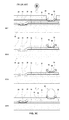
- FIGS. 3 a to 3 c are schematic cross sectional views for showing a method of manufacturing a wafer level package according to the prior art.
- Example aspects of the invention may comprise a semiconductor wafer comprising a plurality of semiconductor die and a plating structure for forming an under bump metal on redistribution layers on the plurality of semiconductor die.
- the plating structure may comprise a plating connection line around a periphery of the semiconductor wafer, and a plating bar coupling the plating connection line to plating traces on the plurality of semiconductor die.
- the plating traces may be electrically coupled to the redistribution layers on the plurality of semiconductor die.
- the semiconductor wafer may comprise a reconstituted wafer of said semiconductor die.
- the semiconductor wafer may comprise a wafer prior to singulating the plurality of semiconductor die.
- the plating bar may be located in a sawing line for the singulating of the plurality of semiconductor die.
- a passivation layer may cover the redistribution layer and the plating traces.
- the under bump metal may be formed in an opening in the passivation layer.
- the plating structure may comprise an electrode terminal for a plating process for forming the under bump metal.
- the under bump metal may comprise one or more of nickel, gold, and copper.
- An input/output terminal may be formed on the under bump metal.
- the input/output terminal may comprise a solder bump.
- the present invention has been made to solve the above-mentioned problems occurring in the prior art, and the present invention provides a wafer level package and a method of manufacturing the wafer level package by using the same, which is capable of reducing the number of the sputtering process for a seed layer to be used in the formation of the typical under bump metal (UBM), the number of the patterning processes and the exposure processes involved in photoresist processing, and the number of the etching processes for the seed layer, resulting in a reduction of the manufacturing cost and manufacturing time, by simultaneously forming plating structures to be connected with a redistribution layer and a bonding pad of the chip during the plating of the redistribution layer, and by using the plating structure as a plating line for forming the UBM.
- UBM under bump metal
- FIGS. 3 a to 3 c are sequence diagrams for showing the method of manufacturing a Wafer Level Chip Scale Package (WLCSP) according to the prior art.
- WLCSP Wafer Level Chip Scale Package
- a designed circuit is integrated on a semiconductor chip ( 10 ) that is still present at a wafer level.
- a bonding pad ( 12 ) is formed at a predetermined area on the wafer, which is corresponding to an electrical input/output path of the circuit.
- a die passivation ( 14 ) for protecting the integrated circuit is formed over the total surface of the respective semiconductor chip ( 10 ), but is not provided on the bonding pad ( 12 ).
- a step of forming a first passivation film ( 16 ) so as to create a redistribution layer on the die passivation ( 14 ) proceeds (step S 202 ).
- the first passivation film ( 16 ) may not be coated on a plurality of metal pads formed at an adequate arrangement, that is, on the bonding pad ( 12 ).
- the reason is that an end of a redistribution layer ( 18 ) is conductively connected to the bonding pad ( 12 ).
- the redistribution layer ( 18 ) comprises a metal distribution layer for receiving an electric voltage required to operate the circuit integrated on the semiconductor chip.
- a first seed layer ( 20 ) is formed on upper surfaces of the first passivation film ( 16 ) and the bonding pad ( 12 ) by using the sputtering process (step S 203 ).
- the first seed layer ( 20 ) comprises a conductive line for forming the redistribution layer ( 18 ).
- a first photoresist ( 22 ) is coated on the surface of the semiconductor chip ( 10 ) and then areas of the semiconductor chip ( 10 ) where the bonding pad ( 12 ) and the redistribution layer ( 18 ) may be formed, are externally exposed by performing the typical exposure and development process (step S 204 ). At this time, the first seed layer ( 20 ) has been already formed at the exposed areas, which are corresponding to the bonding pad ( 12 ) and the redistribution layer ( 18 ).
- an electroplating process of forming the redistribution layer ( 18 ) at the exposed areas proceeds (step S 205 ).
- an electric current is applied to the first seed layer ( 20 ) when the first seed layer ( 20 ) is dipped into a solution comprising metal ions, then the exposed areas on the surface of the first seed layer ( 20 ), which is corresponding to the bonding pad ( 12 ) and the redistribution layer ( 18 ), are plated with metal ions, thereby resulting in the formation of the redistribution layer ( 18 ).
- a process of stripping the first photoresist ( 22 ) proceeds (step S 206 ), and then a process of removing a part of the first seed layer ( 20 ), except for the other part of the first seed layer ( 20 ) down below the redistribution layer( 18 ), proceeds by using an etching process (step S 207 ), thereby resulting in the completion of the redistribution layer ( 18 ) having a predetermined surface area and a predetermined length.
- one end of the redistribution layer ( 18 ) is conductively connected to the bonding pad ( 12 ) and the other end of the redistribution layer ( 18 ) extends to a predetermined site on which the input/output terminal ( 32 ) such as a solder ball may be attached.
- the redistribution layer ( 18 ) comprises a metal distribution layer which extends from the bonding pad ( 12 ) to the outside so as to allow the input/output terminals ( 32 ) to be attached to the bonding pad ( 12 ) while maintaining a wider gap there between.
- a step of forming a second passivation film ( 24 ) on upper surfaces of the first passivation film ( 16 ) and the redistribution layer ( 18 ) proceeds (step S 208 ).
- the second passivation film ( 24 ) is not provided on the other end of the redistribution layer ( 18 ) so as to allow the input/output terminal ( 32 ) to be attached thereto.
- the second passivation film ( 24 ) is made of the same materials and the same method as those used in the process of forming the first passivation film ( 16 ).
- the second passivation layer functions to prevent moisture and other foreign substances from being permeated into the redistribution layer ( 18 ) and to prevent a mechanical shock from being transmitted to the redistribution layer ( 18 ).
- the second passivation layer ( 24 ) functions to prevent an electrical short between the redistribution layers from being occurred.
- a under-bump-metal that is, an electrode terminal made of a metal material on the other end of the redistribution layer ( 18 ) by using the plating structure ( 40 )
- a second seed layer ( 26 ) is formed over the surface of the exposed other end of the redistribution layer ( 18 ) and the second passivation film ( 24 ) by performing the sputtering process (step S 209 ).
- a second photoresist ( 28 ) is coated over the upper surfaces of the other end of the redistribution layer ( 18 ) and the second passivation film ( 24 ) and thereafter the other end of the redistribution layer ( 18 ) is externally exposed by performing an exposure and development process (step S 210 ).
- the UBM ( 30 ) is formed on the surface of the second seed layer ( 26 ), which is externally exposed at the redistribution layer ( 18 ). At this time, the UBM ( 30 ) functions as a pad for allowing the input/output terminal to be easily melted and attached to the surface of the second seed layer ( 26 ).
- the UBM ( 30 ) is made of nickel or gold, which can be easily connected to the input/output terminal such as the solder ball. Alternatively, the UBM ( 30 ) can be formed as a thick layer by using copper plating.
- the second photoresist ( 28 ) may be stripped (step S 212 ), and then the second seed layer ( 26 ) is removed except for a part of the second seed layer ( 26 ) down below the UBM ( 30 ) utilizing an etching process (step S 213 ).
- the UBM( 30 ) may be formed at a predetermined site where the input/output terminal ( 32 ) such as a solder ball may be attached.
- the input/output terminal ( 32 ), such as the solder ball, may be melted and then attached to the UBM( 30 ) in step S 214 , and thereby resulting in the completion of the Wafer Level Package.
- the manufacturing process of the Wafer Level Package it is necessary to perform the sputtering process at two times for the purpose of forming the first seed layer for plating the redistribution layer and the second seed layer for plating the UBM; the PI patterning process for the first photoresist and the typical exposure and development process; the PI patterning process for the second photoresist and the typical exposure and development process; the stripping process for removing the first and second photoresists at two times after performing the patterning process; and the etching process for removing the first and second seed layers at two times. Accordingly, it is essential that a large number of the manufacturing processes are performed in the above described process. Also, the production time of the Wafer Level Package is too long, leading to a large increase of the manufacturing cost.
- the second seed layer for plating it is required to make the second seed layer for plating, apply the second photoresist to the surface of the second passivation film, and to perform the exposure and development process, thereby resulting in the increased number of the manufacturing processes and of the manufacturing cost.
- a plating device for manufacturing a Wafer Level Package comprising: a plating structure to be used in a process of plating a UBM, which may comprise a post-treatment process in forming a redistribution layer in Wafer Level Semiconductor Package, wherein the plating structure may extend from a bonding pad of the respective chip that is a reconstituted wafer or from the redistribution layer to a sawing line of a wafer at the same time as the plating of the redistribution layer.
- the plating structure comprises a plating trace extending from the bonding pad of the chip or the redistribution layer through and beyond an edge of the chip to the sawing line of the wafer; and a plating bar extending along the sawing line of the wafer and integrally connecting each respective plating trace together.
- the plating structure further comprises a plating connection line being integrally connected with the plating bar and extending along the edge of the wafer.
- a method of manufacturing a Wafer Level Package by using a plating device for manufacturing a Wafer Level Package comprising the steps of: providing a wafer; forming a first passivation film on a surface of the respective chip that is a reconstituted wafer, except for a bonding pad; forming a first seed layer for redistribution plating on upper surfaces of the first passivation film and the bonding pad; exposing the bonding pad of the chip, an area on which the redistribution layer may be formed, and an area on which the plating structure may be formed, by performing the exposure and development process, after coating a first photoresist over the surface of the first passivation film.
- the redistribution layer may be formed on a part of the first seed layer, which may be on the exposed bonding pad of the chip and the area on which the exposed redistribution layer may be formed, and at the same time forming the plating structure on the other part of the first seed layer, which may be on the area on which the plating structure may be formed, due to the use of the electroplating process.
- a portion of the first seed layer may be removed, except for the other portion of the first seed layer below the redistribution layer and the plating structure.
- a second passivation film may be applied on other areas of the chip, except for one end of the redistribution layer on which a UBM may be formed, and the end of the redistribution layer with the UBM that is a metallic electrode terminal may be plated by applying an electrical current to the plating structure.
- the UBM may comprise a conductive metal selected from the group consisting of nickel, gold and copper.
- the conductive metal may be suitable to combine with an input/output terminal such as a solder ball as a metallic bond.
- the plating bar may be removed together with a part of the plating trace of the plating structure by sawing the respective chip that is a reconstituted wafer along the sawing line.
- the number of sputtering processes may be reduced for a seed layer to be used in the formation of the UBM, the number of the patterning processes and the exposure processes involved in photoresist processing, as well as the number of etching processes for the seed layer, thereby resulting in the reduction of the manufacturing cost and the manufacturing time, by simultaneously forming plating structures to be connected with a redistribution layer, and a bonding pad of the chip during the plating of the redistribution layer, and by using the plating structure as a plating line for forming the UBM.
- aspects of the present invention may be applied to manufacturing processes for all types of packages, such as Wafer Level Chip Scale Package (WLCSP), Wafer Level Fan-Out Package, and Wafer Level Fan-In Package, where processes of forming a redistribution layer and a plating process may be involved.
- WLCSP Wafer Level Chip Scale Package
- Fan-Out Package Wafer Level Fan-Out Package
- Wafer Level Fan-In Package processes of forming a redistribution layer and a plating process may be involved.
- FIGS. 1 a and 1 b are sequence diagrams showing the method of manufacturing a wafer level package according to an example embodiment of the present invention.
- the method of manufacturing a wafer level package according to an example embodiment of the present invention several steps from the step of providing a wafer to the step of forming a redistribution layer may be performed in the same way as those of the method of manufacturing a wafer level package described above.
- the whole process of an example embodiment of the present invention will be explained in regular sequence for the sake of better understanding.
- a designed circuit was integrated on a semiconductor chip ( 10 ) that may still be present at a wafer level. Furthermore, a bonding pad ( 12 ) may be formed at a predetermined area of the semiconductor chip ( 10 ), which may correspond to an electrical input/output path of the circuit.
- a die passivation ( 14 ) for protecting the integrated circuit may be formed on the total surface of the respective semiconductor chip ( 10 ) that may be present at a wafer level.
- the die passivation ( 14 ) may comprise an opening for the bonding pad ( 12 ) for electrical input/output.
- a first passivation film ( 16 ) may be formed so as to create a redistribution layer on the die passivation ( 14 ) of the semiconductor chip ( 10 ) (step S 102 ).
- the first passivation film ( 16 ) may comprise openings on a plurality of metal pads formed in a desired arrangement, for example, on the bonding pad ( 12 ), such that an end of a redistribution layer( 18 ) may be conductively connected to the bonding pad ( 12 ).
- the redistribution layer ( 18 ) may comprise a metal distribution layer for receiving an electric voltage required to operate the circuit integrated on the semiconductor chip.
- a first seed layer ( 20 ) may be formed on upper surfaces of the first passivation film ( 16 ) and the bonding pad ( 12 ) by using the sputtering process (step S 103 ).
- the first seed layer ( 20 ) may comprise a conductive line for forming the redistribution layer ( 18 ).
- the plating device which may be used in the formation process of UBM in the post-treatment process, may be used in the process of forming the redistribution layer.
- a plurality of chips, which have yet to be sawn at a wafer level, may be disposed with predetermined intervals between sawing lines.
- a plating structure ( 40 ) for forming the UBM may be formed at the time that the redistribution layer ( 18 ) is formed on the semiconductor chip( 10 ), which may still be present at a wafer level.
- the plating structure ( 40 ) may comprise a plating trace ( 42 ) extending from the bonding pad ( 12 ) of the chip ( 10 ) or the redistribution layer ( 18 ) through and beyond an edge of the chip ( 10 ) to the sawing line of the wafer; and a plating bar ( 44 ) extending along the sawing line of the wafer and integrally connecting each respective plating trace ( 42 ) together.
- the plating structure ( 40 ) as described above may be formed simultaneously with the redistribution layer ( 18 ) while performing the electrical plating process.
- a first photoresist ( 22 ) may be coated over a surface of the semiconductor chip ( 10 ) that is still present at a wafer level, that is, the surface of the first passivation film ( 16 ). Thereafter, the conventional exposure and development process may be performed so that areas of the semiconductor chip on which the bonding pad ( 12 ) and the redistribution layer ( 18 ) to be formed may be externally exposed. At the same time, areas on which the plating trace ( 42 ), the plating bar ( 44 ) and the plating connection line ( 46 ) of the plating structure ( 40 ) are to be formed may be externally exposed (step S 104 ).
- the first seed layer ( 20 ) for plating may have already been formed on the bonding pad ( 12 ) of the semiconductor chip ( 10 ) that is externally exposed, the area on which the redistribution layer is to be formed, and the area on which the plating structure ( 40 ) may be formed, by using the sputtering process.
- the redistribution layer may then be formed on the areas on which the redistribution layer ( 18 ) and the bonding pad ( 12 ) of the semiconductor chip ( 10 ) are to be formed.
- an electroplating process for forming the plating structure ( 40 ) may be performed (step S 105 ).
- the exposed areas on the surface of the first seed layer ( 20 ), which is corresponding to the bonding pad ( 12 ) and the redistribution layer ( 18 ), may be plated with metal ions, resulting in the formation of the redistribution layer ( 18 ) on the surface of the first seed layer ( 20 ).
- a plating structure ( 40 ) may be provided on the surface of the first seed layer ( 20 ).
- the first photoresist ( 22 ) may be stripped (step S 106 ) and then a part of the first seed layer ( 20 ) may be removed by etching, except for the part of the first seed layer ( 20 ) beneath the redistribution layer ( 18 ) (step S 106 ), thereby completing the redistribution layer ( 18 ) having a predetermined surface area and a predetermined length.
- the plating structure ( 40 ) to be used in the step of forming the UBM has been completed.
- one end of the redistribution layer ( 18 ) may be conductively connected to the bonding pad ( 12 ) and the other end of the redistribution layer ( 18 ) may extend to a predetermined site on which the input/output terminal ( 32 ), such as a solder ball, may be attached.
- second passivation film ( 24 ) may be formed on upper surfaces of the first passivation film ( 16 ) and the redistribution layer ( 18 ) (step S 107 ). At this time, the second passivation film ( 24 ) may comprise an opening at the other end of the redistribution layer ( 18 ) so as to allow the input/output terminal ( 32 ) to be attached thereto.
- the second passivation film ( 24 ) may comprise the same materials and be formed using the same method as those used in the process of forming the first passivation film ( 16 ).
- the second passivation layer may function to prevent moisture and other foreign substances from permeating into the redistribution layer ( 18 ) and to prevent mechanical shock from being transmitted to the redistribution layer ( 18 ).
- the second passivation layer ( 24 ) may function to prevent an electrical short between the redistribution layers.
- the UBM ( 30 ) may be formed, that is, an electrode terminal made of a metal material is formed, at the other end of the redistribution layer ( 18 ) using the plating structure ( 40 ) (step S 108 ).
- the UBM ( 30 ) may be coated on the other end of the redistribution layer ( 18 ) on which the second passivation film ( 24 ) is not provided, that is an area where the UBM is to be formed.
- the UBM ( 30 ) may comprise metal materials such as Ni, Au and so on, which may be easily combined with the input/output terminal such as a solder ball.
- the UBM ( 30 ) may comprise other conductive metal materials.
- the input/output terminal ( 32 ) such as a solder ball, may be melted attaching it to the UBM ( 30 ) using a solder reflow process, thereby resulting in the completion of the wafer level package according to the present invention.
- the respective scale package may be completed by sawing the respective chip at a wafer-level along the sawing line.
- the plating bar ( 44 ) including a part extending to the sawing line beyond the edge of the chip of the plating trace ( 42 ) of the plating structure ( 40 ), may be cut and then removed by means of sawing tool.
- the wafer level package of an example embodiment of the present invention as described above, it is possible to reduce the number of sputtering process steps for forming the seed layer in order to form the UBM, the number of patterning processes, exposure processes for the photoresist, stripping processes, and the number of etching processes for the seed layer, thereby resulting in a reduction in the number of manufacturing processes and the manufacturing time. Consequently, this leads to the reduction of the manufacturing cost.
- a semiconductor package and manufacturing method thereof may comprise a semiconductor wafer comprising a plurality of semiconductor die and a plating structure for forming an under bump metal on redistribution layers on the plurality of semiconductor die.
- the plating structure may comprise a plating connection line around a periphery of the semiconductor wafer, and a plating bar coupling the plating connection line to plating traces on the plurality of semiconductor die.
- the plating traces may be electrically coupled to the redistribution layers on the plurality of semiconductor die.
- the semiconductor wafer may comprise a reconstituted wafer of said semiconductor die.
- the semiconductor wafer may comprise a wafer prior to singulating the plurality of semiconductor die.
- the plating bar may be located in a sawing line for the singulating of the plurality of semiconductor die.
- a passivation layer may cover the redistribution layer and the plating traces.
- the under bump metal may be formed in an opening in the passivation layer.
- the plating structure may comprise an electrode terminal for a plating process for forming the under bump metal.
- the under bump metal may comprise one or more of nickel, gold, and copper.
- An input/output terminal may be formed on the under bump metal.
- the input/output terminal may comprise a solder bump.
Landscapes
- Engineering & Computer Science (AREA)
- Microelectronics & Electronic Packaging (AREA)
- Computer Hardware Design (AREA)
- Power Engineering (AREA)
- Physics & Mathematics (AREA)
- Condensed Matter Physics & Semiconductors (AREA)
- General Physics & Mathematics (AREA)
- Internal Circuitry In Semiconductor Integrated Circuit Devices (AREA)
- Manufacturing & Machinery (AREA)
Abstract
Description
- 10: semiconductor chip
- 12: bonding pad
- 14: die passivation
- 16: first passivation film
- 18: redistribution layer
- 20: first seed layer
- 22: first photoresist
- 24: second passivation film
- 26: second seed layer
- 28: second photoresist
- 30: UBM
- 32: input/output terminal
- 40: plating structure
- 42: plating trace
- 44: plating bar
- 46: plating connection line
Claims (20)
Applications Claiming Priority (3)
| Application Number | Priority Date | Filing Date | Title |
|---|---|---|---|
| KR10-2012-0100857 | 2012-09-12 | ||
| KR10-2013-0100857 | 2012-09-12 | ||
| KR1020120100857A KR101404464B1 (en) | 2012-09-12 | 2012-09-12 | Plating structure and Method for manufacturing semiconductor package using the same |
Publications (2)
| Publication Number | Publication Date |
|---|---|
| US20140070408A1 US20140070408A1 (en) | 2014-03-13 |
| US9070675B2 true US9070675B2 (en) | 2015-06-30 |
Family
ID=50237860
Family Applications (1)
| Application Number | Title | Priority Date | Filing Date |
|---|---|---|---|
| US13/973,492 Active US9070675B2 (en) | 2012-09-12 | 2013-08-22 | Plating structure for wafer level packages |
Country Status (2)
| Country | Link |
|---|---|
| US (1) | US9070675B2 (en) |
| KR (1) | KR101404464B1 (en) |
Families Citing this family (5)
| Publication number | Priority date | Publication date | Assignee | Title |
|---|---|---|---|---|
| US10204876B2 (en) * | 2013-03-07 | 2019-02-12 | Maxim Integrated Products, Inc. | Pad defined contact for wafer level package |
| US11018025B2 (en) * | 2015-07-31 | 2021-05-25 | Taiwan Semiconductor Manufacturing Company, Ltd. | Redistribution lines having stacking vias |
| KR101743467B1 (en) | 2015-08-24 | 2017-06-07 | 주식회사 에스에프에이반도체 | Method for manfacturing fan-out type wafer level package |
| CN112420534B (en) * | 2020-11-27 | 2021-11-23 | 上海易卜半导体有限公司 | Method for forming semiconductor package and semiconductor package |
| CN112687619A (en) | 2020-12-25 | 2021-04-20 | 上海易卜半导体有限公司 | Method for forming semiconductor package and semiconductor package |
Citations (1)
| Publication number | Priority date | Publication date | Assignee | Title |
|---|---|---|---|---|
| US7977783B1 (en) * | 2009-08-27 | 2011-07-12 | Amkor Technology, Inc. | Wafer level chip size package having redistribution layers |
Family Cites Families (1)
| Publication number | Priority date | Publication date | Assignee | Title |
|---|---|---|---|---|
| KR20080011617A (en) * | 2006-07-31 | 2008-02-05 | 주식회사 하이닉스반도체 | Wafer level chip size package and manufacturing method thereof |
-
2012
- 2012-09-12 KR KR1020120100857A patent/KR101404464B1/en active Active
-
2013
- 2013-08-22 US US13/973,492 patent/US9070675B2/en active Active
Patent Citations (1)
| Publication number | Priority date | Publication date | Assignee | Title |
|---|---|---|---|---|
| US7977783B1 (en) * | 2009-08-27 | 2011-07-12 | Amkor Technology, Inc. | Wafer level chip size package having redistribution layers |
Also Published As
| Publication number | Publication date |
|---|---|
| US20140070408A1 (en) | 2014-03-13 |
| KR101404464B1 (en) | 2014-06-10 |
| KR20140034491A (en) | 2014-03-20 |
Similar Documents
| Publication | Publication Date | Title |
|---|---|---|
| KR102586078B1 (en) | Semiconductor device and method of manufacturing thereof | |
| KR102024472B1 (en) | A semiconductor device and a method of making a semiconductor device | |
| US8759209B2 (en) | Semiconductor device and method of forming a dual UBM structure for lead free bump connections | |
| US11574890B2 (en) | Semiconductor devices and methods of manufacturing semiconductor devices | |
| US10096540B2 (en) | Semiconductor device and method of forming dummy pillars between semiconductor die and substrate for maintaining standoff distance | |
| CN110085557B (en) | Semiconductor devices and methods of forming embedded wafer level chip size packages using standardized carriers | |
| KR102900717B1 (en) | Semiconductor device and manufacturing method thereof | |
| TWI582921B (en) | Semiconductor package structure and manufacturing method thereof | |
| CN104733379A (en) | Semiconductor device and method of forming fine pitch rdl over semiconductor die in fan-out package | |
| KR20080098335A (en) | Expanded redistribution layer bump wafer semiconductor device and manufacturing method thereof | |
| CN103325696A (en) | Manufacturing method of wafer-level semiconductor package and method of manufacturing wafer-level packaging substrate | |
| US9070675B2 (en) | Plating structure for wafer level packages | |
| KR101624855B1 (en) | Wafer level fan-out package and method for manufacturing the same | |
| US12027483B2 (en) | Packaged semiconductor device with electroplated pillars | |
| US6596611B2 (en) | Method for forming wafer level package having serpentine-shaped electrode along scribe line and package formed | |
| TW202343733A (en) | Semiconductor device and method of forming an embedded redistribution layer | |
| KR101300574B1 (en) | Method for manufacturing semiconductor package |
Legal Events
| Date | Code | Title | Description |
|---|---|---|---|
| AS | Assignment |
Owner name: AMKOR TECHNOLOGY, INC., ARIZONA Free format text: ASSIGNMENT OF ASSIGNORS INTEREST;ASSIGNORS:SO, KWANG SUP;PARK, NO SUN;REEL/FRAME:031075/0865 Effective date: 20130805 |
|
| AS | Assignment |
Owner name: BANK OF AMERICA, N.A., TEXAS Free format text: PATENT SECURITY AGREEMENT;ASSIGNOR:AMKOR TECHNOLOGY, INC.;REEL/FRAME:035613/0592 Effective date: 20150409 |
|
| STCF | Information on status: patent grant |
Free format text: PATENTED CASE |
|
| AS | Assignment |
Owner name: BANK OF AMERICA, N.A., AS AGENT, CALIFORNIA Free format text: SECURITY INTEREST;ASSIGNOR:AMKOR TECHNOLOGY, INC.;REEL/FRAME:046683/0139 Effective date: 20180713 |
|
| MAFP | Maintenance fee payment |
Free format text: PAYMENT OF MAINTENANCE FEE, 4TH YEAR, LARGE ENTITY (ORIGINAL EVENT CODE: M1551); ENTITY STATUS OF PATENT OWNER: LARGE ENTITY Year of fee payment: 4 |
|
| AS | Assignment |
Owner name: AMKOR TECHNOLOGY SINGAPORE HOLDING PTE.LTD., SINGAPORE Free format text: ASSIGNMENT OF ASSIGNORS INTEREST;ASSIGNOR:AMKOR TECHNOLOGY, INC.;REEL/FRAME:054046/0673 Effective date: 20191119 |
|
| MAFP | Maintenance fee payment |
Free format text: PAYMENT OF MAINTENANCE FEE, 8TH YEAR, LARGE ENTITY (ORIGINAL EVENT CODE: M1552); ENTITY STATUS OF PATENT OWNER: LARGE ENTITY Year of fee payment: 8 |