US8993056B2 - Method of gas distribution and nozzle design in the improved chemical vapor deposition of polysilicon reactor - Google Patents
Method of gas distribution and nozzle design in the improved chemical vapor deposition of polysilicon reactor Download PDFInfo
- Publication number
- US8993056B2 US8993056B2 US12/970,562 US97056210A US8993056B2 US 8993056 B2 US8993056 B2 US 8993056B2 US 97056210 A US97056210 A US 97056210A US 8993056 B2 US8993056 B2 US 8993056B2
- Authority
- US
- United States
- Prior art keywords
- silicon
- gas
- gas distribution
- chamber
- distribution chamber
- Prior art date
- Legal status (The legal status is an assumption and is not a legal conclusion. Google has not performed a legal analysis and makes no representation as to the accuracy of the status listed.)
- Expired - Fee Related, expires
Links
- 238000009826 distribution Methods 0.000 title claims abstract description 35
- 238000000034 method Methods 0.000 title claims abstract description 25
- 238000005229 chemical vapour deposition Methods 0.000 title claims abstract description 16
- 229910021420 polycrystalline silicon Inorganic materials 0.000 title claims abstract description 15
- 238000013461 design Methods 0.000 title abstract description 11
- 229920005591 polysilicon Polymers 0.000 title abstract description 9
- 229910052710 silicon Inorganic materials 0.000 claims abstract description 48
- 239000010703 silicon Substances 0.000 claims abstract description 48
- XUIMIQQOPSSXEZ-UHFFFAOYSA-N Silicon Chemical group [Si] XUIMIQQOPSSXEZ-UHFFFAOYSA-N 0.000 claims abstract description 41
- 230000008569 process Effects 0.000 claims abstract description 20
- 238000000151 deposition Methods 0.000 claims abstract description 16
- 230000008021 deposition Effects 0.000 claims abstract description 15
- 238000006243 chemical reaction Methods 0.000 claims description 19
- 238000010438 heat treatment Methods 0.000 claims description 6
- 238000002955 isolation Methods 0.000 claims description 6
- 238000012546 transfer Methods 0.000 claims description 6
- 239000012530 fluid Substances 0.000 claims description 5
- 238000004519 manufacturing process Methods 0.000 claims description 5
- 239000013529 heat transfer fluid Substances 0.000 claims description 4
- 238000000429 assembly Methods 0.000 claims description 2
- 230000000712 assembly Effects 0.000 claims description 2
- 230000001737 promoting effect Effects 0.000 abstract 1
- 239000007789 gas Substances 0.000 description 63
- BLRPTPMANUNPDV-UHFFFAOYSA-N Silane Chemical compound [SiH4] BLRPTPMANUNPDV-UHFFFAOYSA-N 0.000 description 9
- 229910000077 silane Inorganic materials 0.000 description 8
- 238000000354 decomposition reaction Methods 0.000 description 7
- 239000000463 material Substances 0.000 description 7
- 239000002243 precursor Substances 0.000 description 7
- 230000006911 nucleation Effects 0.000 description 6
- 238000010899 nucleation Methods 0.000 description 6
- 239000000843 powder Substances 0.000 description 6
- UFHFLCQGNIYNRP-UHFFFAOYSA-N Hydrogen Chemical compound [H][H] UFHFLCQGNIYNRP-UHFFFAOYSA-N 0.000 description 5
- 239000002245 particle Substances 0.000 description 5
- -1 silicon halides Chemical class 0.000 description 5
- 239000000758 substrate Substances 0.000 description 5
- 239000006227 byproduct Substances 0.000 description 4
- 150000001875 compounds Chemical class 0.000 description 4
- 229910052739 hydrogen Inorganic materials 0.000 description 4
- 239000001257 hydrogen Substances 0.000 description 4
- VXEGSRKPIUDPQT-UHFFFAOYSA-N 4-[4-(4-methoxyphenyl)piperazin-1-yl]aniline Chemical compound C1=CC(OC)=CC=C1N1CCN(C=2C=CC(N)=CC=2)CC1 VXEGSRKPIUDPQT-UHFFFAOYSA-N 0.000 description 3
- 239000000203 mixture Substances 0.000 description 3
- 239000000376 reactant Substances 0.000 description 3
- 239000005049 silicon tetrachloride Substances 0.000 description 3
- ZDHXKXAHOVTTAH-UHFFFAOYSA-N trichlorosilane Chemical compound Cl[SiH](Cl)Cl ZDHXKXAHOVTTAH-UHFFFAOYSA-N 0.000 description 3
- 239000005052 trichlorosilane Substances 0.000 description 3
- 238000009825 accumulation Methods 0.000 description 2
- 150000004820 halides Chemical class 0.000 description 2
- 230000007246 mechanism Effects 0.000 description 2
- 230000002028 premature Effects 0.000 description 2
- 238000002360 preparation method Methods 0.000 description 2
- 239000000047 product Substances 0.000 description 2
- 238000011084 recovery Methods 0.000 description 2
- 238000004088 simulation Methods 0.000 description 2
- OKTJSMMVPCPJKN-UHFFFAOYSA-N Carbon Chemical compound [C] OKTJSMMVPCPJKN-UHFFFAOYSA-N 0.000 description 1
- ZAMOUSCENKQFHK-UHFFFAOYSA-N Chlorine atom Chemical compound [Cl] ZAMOUSCENKQFHK-UHFFFAOYSA-N 0.000 description 1
- 229910003818 SiH2Cl2 Inorganic materials 0.000 description 1
- 229910003826 SiH3Cl Inorganic materials 0.000 description 1
- 238000013459 approach Methods 0.000 description 1
- 230000009286 beneficial effect Effects 0.000 description 1
- 230000008901 benefit Effects 0.000 description 1
- 229910052799 carbon Inorganic materials 0.000 description 1
- 239000000460 chlorine Substances 0.000 description 1
- 229910052801 chlorine Inorganic materials 0.000 description 1
- 150000001805 chlorine compounds Chemical class 0.000 description 1
- 125000001309 chloro group Chemical group Cl* 0.000 description 1
- SLLGVCUQYRMELA-UHFFFAOYSA-N chlorosilicon Chemical compound Cl[Si] SLLGVCUQYRMELA-UHFFFAOYSA-N 0.000 description 1
- 238000011109 contamination Methods 0.000 description 1
- 238000005137 deposition process Methods 0.000 description 1
- 230000000694 effects Effects 0.000 description 1
- 230000005484 gravity Effects 0.000 description 1
- 238000003306 harvesting Methods 0.000 description 1
- 238000005259 measurement Methods 0.000 description 1
- 230000008018 melting Effects 0.000 description 1
- 238000002844 melting Methods 0.000 description 1
- 238000012986 modification Methods 0.000 description 1
- 230000004048 modification Effects 0.000 description 1
- 238000000197 pyrolysis Methods 0.000 description 1
- 230000005855 radiation Effects 0.000 description 1
- 239000012495 reaction gas Substances 0.000 description 1
- 230000008707 rearrangement Effects 0.000 description 1
- 230000000630 rising effect Effects 0.000 description 1
- 239000012686 silicon precursor Substances 0.000 description 1
- 238000006467 substitution reaction Methods 0.000 description 1
- 238000009827 uniform distribution Methods 0.000 description 1
- 239000002699 waste material Substances 0.000 description 1
Images


Classifications
-
- C—CHEMISTRY; METALLURGY
- C23—COATING METALLIC MATERIAL; COATING MATERIAL WITH METALLIC MATERIAL; CHEMICAL SURFACE TREATMENT; DIFFUSION TREATMENT OF METALLIC MATERIAL; COATING BY VACUUM EVAPORATION, BY SPUTTERING, BY ION IMPLANTATION OR BY CHEMICAL VAPOUR DEPOSITION, IN GENERAL; INHIBITING CORROSION OF METALLIC MATERIAL OR INCRUSTATION IN GENERAL
- C23C—COATING METALLIC MATERIAL; COATING MATERIAL WITH METALLIC MATERIAL; SURFACE TREATMENT OF METALLIC MATERIAL BY DIFFUSION INTO THE SURFACE, BY CHEMICAL CONVERSION OR SUBSTITUTION; COATING BY VACUUM EVAPORATION, BY SPUTTERING, BY ION IMPLANTATION OR BY CHEMICAL VAPOUR DEPOSITION, IN GENERAL
- C23C16/00—Chemical coating by decomposition of gaseous compounds, without leaving reaction products of surface material in the coating, i.e. chemical vapour deposition [CVD] processes
- C23C16/22—Chemical coating by decomposition of gaseous compounds, without leaving reaction products of surface material in the coating, i.e. chemical vapour deposition [CVD] processes characterised by the deposition of inorganic material, other than metallic material
- C23C16/24—Deposition of silicon only
-
- C—CHEMISTRY; METALLURGY
- C01—INORGANIC CHEMISTRY
- C01B—NON-METALLIC ELEMENTS; COMPOUNDS THEREOF; METALLOIDS OR COMPOUNDS THEREOF NOT COVERED BY SUBCLASS C01C
- C01B33/00—Silicon; Compounds thereof
- C01B33/02—Silicon
- C01B33/021—Preparation
- C01B33/027—Preparation by decomposition or reduction of gaseous or vaporised silicon compounds other than silica or silica-containing material
- C01B33/035—Preparation by decomposition or reduction of gaseous or vaporised silicon compounds other than silica or silica-containing material by decomposition or reduction of gaseous or vaporised silicon compounds in the presence of heated filaments of silicon, carbon or a refractory metal, e.g. tantalum or tungsten, or in the presence of heated silicon rods on which the formed silicon is deposited, a silicon rod being obtained, e.g. Siemens process
-
- C—CHEMISTRY; METALLURGY
- C23—COATING METALLIC MATERIAL; COATING MATERIAL WITH METALLIC MATERIAL; CHEMICAL SURFACE TREATMENT; DIFFUSION TREATMENT OF METALLIC MATERIAL; COATING BY VACUUM EVAPORATION, BY SPUTTERING, BY ION IMPLANTATION OR BY CHEMICAL VAPOUR DEPOSITION, IN GENERAL; INHIBITING CORROSION OF METALLIC MATERIAL OR INCRUSTATION IN GENERAL
- C23C—COATING METALLIC MATERIAL; COATING MATERIAL WITH METALLIC MATERIAL; SURFACE TREATMENT OF METALLIC MATERIAL BY DIFFUSION INTO THE SURFACE, BY CHEMICAL CONVERSION OR SUBSTITUTION; COATING BY VACUUM EVAPORATION, BY SPUTTERING, BY ION IMPLANTATION OR BY CHEMICAL VAPOUR DEPOSITION, IN GENERAL
- C23C16/00—Chemical coating by decomposition of gaseous compounds, without leaving reaction products of surface material in the coating, i.e. chemical vapour deposition [CVD] processes
- C23C16/44—Chemical coating by decomposition of gaseous compounds, without leaving reaction products of surface material in the coating, i.e. chemical vapour deposition [CVD] processes characterised by the method of coating
- C23C16/455—Chemical coating by decomposition of gaseous compounds, without leaving reaction products of surface material in the coating, i.e. chemical vapour deposition [CVD] processes characterised by the method of coating characterised by the method used for introducing gases into reaction chamber or for modifying gas flows in reaction chamber
- C23C16/45517—Confinement of gases to vicinity of substrate
-
- C—CHEMISTRY; METALLURGY
- C23—COATING METALLIC MATERIAL; COATING MATERIAL WITH METALLIC MATERIAL; CHEMICAL SURFACE TREATMENT; DIFFUSION TREATMENT OF METALLIC MATERIAL; COATING BY VACUUM EVAPORATION, BY SPUTTERING, BY ION IMPLANTATION OR BY CHEMICAL VAPOUR DEPOSITION, IN GENERAL; INHIBITING CORROSION OF METALLIC MATERIAL OR INCRUSTATION IN GENERAL
- C23C—COATING METALLIC MATERIAL; COATING MATERIAL WITH METALLIC MATERIAL; SURFACE TREATMENT OF METALLIC MATERIAL BY DIFFUSION INTO THE SURFACE, BY CHEMICAL CONVERSION OR SUBSTITUTION; COATING BY VACUUM EVAPORATION, BY SPUTTERING, BY ION IMPLANTATION OR BY CHEMICAL VAPOUR DEPOSITION, IN GENERAL
- C23C16/00—Chemical coating by decomposition of gaseous compounds, without leaving reaction products of surface material in the coating, i.e. chemical vapour deposition [CVD] processes
- C23C16/44—Chemical coating by decomposition of gaseous compounds, without leaving reaction products of surface material in the coating, i.e. chemical vapour deposition [CVD] processes characterised by the method of coating
- C23C16/455—Chemical coating by decomposition of gaseous compounds, without leaving reaction products of surface material in the coating, i.e. chemical vapour deposition [CVD] processes characterised by the method of coating characterised by the method used for introducing gases into reaction chamber or for modifying gas flows in reaction chamber
- C23C16/45563—Gas nozzles
Definitions
- the present invention relates to a novel method for the gas distribution in the chemical vapor deposition (CVD) of a polysilicon reactor.
- the present invention relates to the gas distribution nozzle design and arrangement along the length of the chunk rod for producing polysilicon chunk materials via the decomposition of gaseous silane precursors.
- the production of polysilicon chunk materials via the decomposition of a gaseous precursor compound on a slim rod substrate is a well-known, widely used process commonly referred to as the “Siemens process.”
- the Siemens process is a combined decomposition/deposition process that comprises: (1) a heated rod or rods (appropriate substrates) covered by a suitable enclosure to allow high temperature, air-tight operation; (2) a system to feed the precursor material or compound of desired composition without contamination; (3) heating the enclosed rods to a desired temperature under appropriate environment; (4) decomposing the precursor material preferentially on the heated surface of the rods/substrate by distributing the gas appropriately near the growing rod vicinity; (5) recovery or disposal of byproduct or gases; and (6) recovery of product without contaminating the product.
- the reactant gas is fed to the rods from a single port/nozzle resulting in uneven growth.
- Such uneven gas distribution over the length of the rod further promotes heavy homogeneous nucleation.
- Such uneven growth and homogeneous nucleation promote eventual reactor failure.
- the rods within typical Siemens process reactors are not individually isolated. That makes the distribution of gas very difficult along the length of the rod that is growing. As a result, homogeneous nucleation, lower conversion, higher by-products, and uneven growth on the rods is further promoted by uneven radiant heat between the rods and gas precursor distribution.
- elemental pure silicon is obtained in the Siemens type reactor, in the form of cylindrical rods of high purity by decomposing silicon halides from the distributed gas phase at a hot surface of the pure and purified silicon filament, the preferred halides being the chlorides, silicon tetrachloride and trichlorosilane.
- the preferred halides being the chlorides, silicon tetrachloride and trichlorosilane.
- These compounds become increasingly unstable at temperatures above about 800° C. and decompose.
- Heterogeneous nucleation, hence silicon deposition starts at about 800° C. and extends to the melting point of silicon at 1420° C. Since the deposition is beneficial only on the substrate, the inner walls of the decomposition chamber must not be exposed to the hot gasses so that there is no waste of valuable reactant gas
- thermophoretic deposition of powder particles on the reactor walls is generally weak resulting in the multiple recirculation of the particles in the gas stream. This deposited powder eventually gets loose and collapse into the reactor, causing premature failure. That is why circulation and distribution of the reactant gas is very important.
- silicon halides used most frequently for the preparation of high purity silicon are silicon tetrachloride and trichlorosilane. These halides will undergo pyrolysis when in contact with the hot surface and deposit elemental silicon. To obtain reasonable and economical yields, however, an excess of hydrogen gas is added to the silicon halide vapor reaction feed gas. Because of its proportionally higher silicon content per unit weight and comparatively lower deposition temperature (i.e., faster kinetics), trichlorosilane will deposit more silicon than silicon tetrachloride and is therefore the preferred material for the Siemens' process for the preparation of polycrystalline silicon.
- Silicon halides with less than three chlorine atoms such as SiH 2 Cl 2 and SiH 3 Cl, in particular, deposit much more silicon per mole of silicon halide consumed in the reaction but are impractical because they are not readily available and thus less desirable economically. In any case, the yield is not more than about 20% and by-product gases are very difficult to handle.
- silane offers itself as an effective silicon precursor and having no chlorine in the molecule improves the silicon to hydrogen ratios of silicon reaction gas mixtures.
- Silane decomposes above about 400° C. forming silicon and hydrogen.
- the byproducts formed are silane and hydrogen which may be readily recycled.
- the higher deposition rates and faster kinetics may require better distribution of the gas otherwise reactor will not work properly.
- faster kinetics means faster depletion of gas resulting in uneven deposition unless the fresh gas is distributed evenly along the growth of the rod.
- Embodiments of the invention provide a gas distribution mechanism where gas is distributed uniformly around the rod and also uniform distribution along the length of the growing silicon rod.
- the gas is introduced tangentially to the chamber and distributed uniformly before rising along the length of the growing silicon rod.
- Embodiments of the invention also provide a fresh gas distribution at the point where silicon concentration depletes for the growth and where it prevents uniform growth on the silicon rod.
- the gas nozzle design to distribute the gas in the silicon rod production apparatus.
- the reactor vessel containing at least one reaction chamber surrounded by a jacket, wherein a pre-heating fluid is circulated in the jacket; one or more electrode assemblies extending into the reaction chamber wherein each electrode assembly comprises a gas inlet, one or more heat transfer fluid inlets/outlets, at least one pair of silicon filaments, the filaments connected to each other at their upper ends with a silicon bridge to form a filament/slim rod assembly, each filament/slim rod assembly enclosed in an isolation jacket; a source of a silicon-bearing gas connected to the interior of the vessel for supplying the gas into the reaction chamber to produce a reaction and to deposit polycrystalline silicon on the filament by chemical vapor deposition thereby producing a rod of polycrystalline silicon; a heat transfer system that is connected to the jacketed reaction chamber that supplies heat transfer fluid to preheat the deposition slim rods; and a power supply.
- Additional steps in the inventive method include preheating gap for the gas before entering the reaction chamber where gas attain the reaction feed temperature. This is necessary to eliminate any temperature gradient in the reaction chamber enclosed in the column that is surrounding the individual growing rods.
- the necessary heat for the gas to attain the temperature is provided by the circulating a heat transfer fluid in the heat transfer system surrounding the slim rods/silicon filaments and also the silicon filaments that is heated by an electric current from the power supply.
- FIG. 1 is a schematic empirical view of an embodiment of a gas distribution chamber assembly for a chemical vapor deposition (CVD) reactor used in the inventive process.
- the nozzle arrangement and distribution also can be seen in the figure.
- FIG. 2 is a cross-section schematic for an embodiment of a gas distributor/rod chamber cross sectional view of FIG. 1 .
- FIG. 3 is two different nozzle design slit to the chamber wall and no slit to the chamber wall to inject the gas into the cluster—this is the cluster of four chambers
- FIG. 4 is a cross-section schematic for an embodiment of a fully loaded model run where uniform temperature distribution/gradient can be seen
- FIG. 5 is a cross-section schematic for an embodiment of a fully loaded model run where uniform velocity distribution/gradient can be seen—uniform growth
- the present invention relates to a novel method for the gas distribution in the chemical vapor deposition (CVD) of polysilicon reactor.
- the present invention relates to the gas distribution nozzle design and arrangement along the length of the chunk rod for producing polysilicon chunk materials via the decomposition of gaseous silane precursors.
- This invention is also a part of a novel method for producing polysilicon chunk materials via the decomposition of a gaseous silane and related gasses precursor compound on a slim silicon rod substrate.
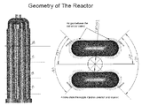
- FIG. 1 is a schematic representative view of an embodiment of a gas distribution chamber assembly for a chemical vapor deposition (CVD) reactor for a cluster of 4 rods used in the inventive process.
- the four isolated chamber contains individual rods, two of each are connected via bridge to complete the circuit.
- outer chamber is heated and transferring the heat to the rods and rods themselves are heated by electric power.
- These chambers surround the gas supply column or chambers as depicted in the figure. As you can see in the figure that there are three different layers or gaps to transferring the gas. The outer gap from gas supply column, the gap between the supply chamber and the rod chamber and the gap within the growing chamber.
- Outer layer is the gas supply column which has certain dimension based on the operation, flow rate and concentration, followed by a gap between the gas supply column and the rod column which also depend on many factors including the flow, concentration and the growth rate. This gap is conveniently depicted so that the gas has sufficient time to attain the reaction temperature.
- 4-rod cluster system the gas is injected tangentially to the rod column so that gas will not impinge on the growing rod thereby creating uneven growth. All 4 rods are injected uniformly and at the same angle for uniform growth. Same pattern continues along the length of the growing rod. This is the first time anywhere, in the Siemens type CVD process, the gas distribution is achieved.
- the nozzles are 8 mm diameter in this growth. However, gap and nozzle diameter can vary with the type of growth. Similarly, number of nozzles can also vary with the concentration, flow rate and growth rate.
- FIG. 2 is a cross-section schematic for an embodiment of a gas distributor/rod chamber cross sectional view of FIG. 1 .
- the nozzle arrangement and distribution also can be seen in the figure. This is the typical arrangement for distribution. As the number of rods in the cluster increases, the distribution can be rearranged.
- the nozzles on the central gas distribution column inject tangentially in the gap between the growth chamber and the gas supply chamber. This gap is very important and critical for the uniform growth. In this case, the width of the gap is 63 mm as shown in the figure. 150 mm diameter is the final rod growth with a outer heated chamber surrounding it.
- FIG. 3 is two different nozzle design slit to the chamber wall and no slit to the chamber wall to inject the gas into the cluster—this is the cluster of four rod chambers.
- FIG. 4 is a cross-section schematic for an embodiment of a fully loaded model run where uniform temperature distribution/gradient can be seen.
- First step to verify our design is runs a full scale flow model to verify the parameters.
- the flow model has computed steady state heat transfer and flow characteristics.
- the model is analyzed all the possible heat transfer mechanisms including conduction, convection and radiation occurring in the growing chamber and beyond.
- a multi-species simulation is carried out; the CVD simulation includes the effect of buoyancy and convection of the gas flow.
- the result depicts the accuracy of our design and uniform temperature distribution around the growing rod. This is very important because if the concentration of the gas species is sufficient, temperature defines the uniformity and efficiency of growth.
- FIG. 5 is a cross-section schematic for an embodiment of a fully loaded model run where uniform velocity distribution/gradient can be seen—uniform growth. This supports earlier model FIG. 4 . If the temperature distribution is uniform, if the velocity profile is uniform, with the controlled gas concentration, one can grow uniform silicon rods with high efficiency.
- the diameter of the nozzle and the gas flow rate in the column is such that the gas should carry out particles formed via homogeneous nucleation.
- the velocity is maintained such that the gas should carry away below 300 ⁇ m particles formed via homogeneous nucleation in the gas phase.
- float zone silicon filaments (approx resistivity ⁇ 200 ⁇ /cm), 2 meters long are inserted into the jacketed cylindrical columns containing the hot circulating fluid.
- the cluster is made from four rods with a growth potential up to 150 mm.
- the silicon filament ends are mounted on a double slide-in carbon chuck that is in touch with the protruded electrode from the base plate.
- the bridge is connected with the slotted slim rods of 300 mm.
- Each of the circular columns has four gas distributing nozzles which inject the gases tangentially along the wall in a circular upward motion.
- the gases are injected in the space between the main heat controlled jacketed column and the distributor column where they will rapidly regain the temperature there by avoiding the cold impingement on the rod and uneven deposition/premature harvesting.
- the measured temperature at the entry point of the growth column is 275° C. which is closer to the outer jacket temperature and inner gas temperature is uniform to that of the growing rod temperature gradient.
- the individual silicon filaments were insulated from each other and maintained at constant hot temperature of 280° C. which is substantially lower than the decomposition temperature of the silane gas.
- the velocity of the gas in the rod chamber was maintained above particle terminal velocity of 5 ft/sec to avoid any homogeneously formed powder accumulation in the reactor system column.
- the gases and all homogeneously formed powder were exhausted from the bottom and collected at high temperature in a bag house. This avoids the typical hazard of powder accumulation at the top of the reactor chamber and subsequent falling of the powder via gravity during the operation which could cause a short circuit.
- the generated gases were purified and re-circulated.
- the rod deposition rate of above 10 ⁇ m/min with the effective diameter of 120 mm gown with this measurement. We have grown up to 150 mm in our other trials.
Landscapes
- Chemical & Material Sciences (AREA)
- Organic Chemistry (AREA)
- General Chemical & Material Sciences (AREA)
- Chemical Kinetics & Catalysis (AREA)
- Engineering & Computer Science (AREA)
- Materials Engineering (AREA)
- Mechanical Engineering (AREA)
- Metallurgy (AREA)
- Inorganic Chemistry (AREA)
- Silicon Compounds (AREA)
Abstract
Description
Claims (7)
Priority Applications (1)
| Application Number | Priority Date | Filing Date | Title |
|---|---|---|---|
| US12/970,562 US8993056B2 (en) | 2009-12-17 | 2010-12-16 | Method of gas distribution and nozzle design in the improved chemical vapor deposition of polysilicon reactor |
Applications Claiming Priority (2)
| Application Number | Priority Date | Filing Date | Title |
|---|---|---|---|
| US28741709P | 2009-12-17 | 2009-12-17 | |
| US12/970,562 US8993056B2 (en) | 2009-12-17 | 2010-12-16 | Method of gas distribution and nozzle design in the improved chemical vapor deposition of polysilicon reactor |
Publications (2)
| Publication Number | Publication Date |
|---|---|
| US20110151137A1 US20110151137A1 (en) | 2011-06-23 |
| US8993056B2 true US8993056B2 (en) | 2015-03-31 |
Family
ID=44151502
Family Applications (1)
| Application Number | Title | Priority Date | Filing Date |
|---|---|---|---|
| US12/970,562 Expired - Fee Related US8993056B2 (en) | 2009-12-17 | 2010-12-16 | Method of gas distribution and nozzle design in the improved chemical vapor deposition of polysilicon reactor |
Country Status (3)
| Country | Link |
|---|---|
| US (1) | US8993056B2 (en) |
| KR (1) | KR20110069739A (en) |
| CN (1) | CN102140678B (en) |
Cited By (1)
| Publication number | Priority date | Publication date | Assignee | Title |
|---|---|---|---|---|
| US12595589B2 (en) | 2022-09-12 | 2026-04-07 | Advanced Material Solutions, Llc | Chemical vapor deposition reactor in polysilicon production process |
Families Citing this family (9)
| Publication number | Priority date | Publication date | Assignee | Title |
|---|---|---|---|---|
| DE202012100839U1 (en) * | 2012-03-08 | 2012-06-22 | Silcontec Gmbh | laboratory reactor |
| CN103482629B (en) * | 2012-06-08 | 2016-01-06 | 半材料株式会社 | Polysilicon deposition apparatus |
| DE102013206236A1 (en) * | 2013-04-09 | 2014-10-09 | Wacker Chemie Ag | Gas distributor for Siemens reactor |
| WO2014208957A1 (en) * | 2013-06-25 | 2014-12-31 | Hanwha Chemical Corporation | Chemical vapor deposition reactor and method for preparing polysilicon |
| US10208381B2 (en) | 2014-12-23 | 2019-02-19 | Rec Silicon Inc | Apparatus and method for managing a temperature profile using reflective energy in a thermal decomposition reactor |
| WO2016106337A1 (en) * | 2014-12-23 | 2016-06-30 | Rec Silicon Inc | Apparatus and method for managing a temperature profile using reflective energy in a thermal decomposition reactor |
| CN109594123A (en) * | 2018-11-12 | 2019-04-09 | 河南硅烷科技发展股份有限公司 | Melt the production technology of level polysilicon stick in a kind of silane legal system area reducing defect |
| CN110255565A (en) * | 2019-07-05 | 2019-09-20 | 江苏双良新能源装备有限公司 | A kind of large size chassis of reducing furnace |
| JP6931751B2 (en) * | 2019-08-02 | 2021-09-08 | 株式会社トクヤマ | Silicon core wire for polycrystalline silicon precipitation and its manufacturing method |
Citations (5)
| Publication number | Priority date | Publication date | Assignee | Title |
|---|---|---|---|---|
| US3057690A (en) * | 1958-12-09 | 1962-10-09 | Siemens Schuckerwerke Ag | Method for producing hyperpure silicon |
| US5478396A (en) * | 1992-09-28 | 1995-12-26 | Advanced Silicon Materials, Inc. | Production of high-purity polycrystalline silicon rod for semiconductor applications |
| US6749824B2 (en) * | 1997-12-15 | 2004-06-15 | Advanced Silicon Materials Llc | Chemical vapor deposition system for polycrystalline silicon rod production |
| US20060086318A1 (en) * | 2004-10-21 | 2006-04-27 | Matsushita Electric Industrial Co., Ltd. | Gas diffusion plate |
| US8399072B2 (en) * | 2009-04-24 | 2013-03-19 | Savi Research, Inc. | Process for improved chemcial vapor deposition of polysilicon |
Family Cites Families (6)
| Publication number | Priority date | Publication date | Assignee | Title |
|---|---|---|---|---|
| CN1393908A (en) * | 2001-06-28 | 2003-01-29 | 旺宏电子股份有限公司 | Manufacturing method of N-type doped polysilicon |
| KR20030038396A (en) * | 2001-11-01 | 2003-05-16 | 에이에스엠엘 유에스, 인코포레이티드 | System and method for preferential chemical vapor deposition |
| KR100688837B1 (en) * | 2005-05-12 | 2007-03-02 | 삼성에스디아이 주식회사 | Chemical Vapor Deposition Apparatus for Crystalline Silicon Deposition |
| JP5509578B2 (en) * | 2007-11-28 | 2014-06-04 | 三菱マテリアル株式会社 | Polycrystalline silicon manufacturing apparatus and manufacturing method |
| US8961689B2 (en) * | 2008-03-26 | 2015-02-24 | Gtat Corporation | Systems and methods for distributing gas in a chemical vapor deposition reactor |
| CN201232028Y (en) * | 2008-04-20 | 2009-05-06 | 徐州东南多晶硅材料研发有限公司 | Polycrystalline silicon reducing furnace with adjustable air inlet pipe nozzle |
-
2010
- 2010-12-16 US US12/970,562 patent/US8993056B2/en not_active Expired - Fee Related
- 2010-12-17 CN CN201010593610.9A patent/CN102140678B/en not_active Expired - Fee Related
- 2010-12-17 KR KR1020100129962A patent/KR20110069739A/en not_active Withdrawn
Patent Citations (5)
| Publication number | Priority date | Publication date | Assignee | Title |
|---|---|---|---|---|
| US3057690A (en) * | 1958-12-09 | 1962-10-09 | Siemens Schuckerwerke Ag | Method for producing hyperpure silicon |
| US5478396A (en) * | 1992-09-28 | 1995-12-26 | Advanced Silicon Materials, Inc. | Production of high-purity polycrystalline silicon rod for semiconductor applications |
| US6749824B2 (en) * | 1997-12-15 | 2004-06-15 | Advanced Silicon Materials Llc | Chemical vapor deposition system for polycrystalline silicon rod production |
| US20060086318A1 (en) * | 2004-10-21 | 2006-04-27 | Matsushita Electric Industrial Co., Ltd. | Gas diffusion plate |
| US8399072B2 (en) * | 2009-04-24 | 2013-03-19 | Savi Research, Inc. | Process for improved chemcial vapor deposition of polysilicon |
Cited By (1)
| Publication number | Priority date | Publication date | Assignee | Title |
|---|---|---|---|---|
| US12595589B2 (en) | 2022-09-12 | 2026-04-07 | Advanced Material Solutions, Llc | Chemical vapor deposition reactor in polysilicon production process |
Also Published As
| Publication number | Publication date |
|---|---|
| US20110151137A1 (en) | 2011-06-23 |
| CN102140678B (en) | 2015-12-09 |
| CN102140678A (en) | 2011-08-03 |
| KR20110069739A (en) | 2011-06-23 |
Similar Documents
| Publication | Publication Date | Title |
|---|---|---|
| US8993056B2 (en) | Method of gas distribution and nozzle design in the improved chemical vapor deposition of polysilicon reactor | |
| US7922990B2 (en) | Method and device for producing granulated polycrystalline silicon in a fluidized bed reactor | |
| EP0324504B1 (en) | Method for forming uniformly large-diameter polycrystalline rods by the pyrolysis of silane and a reactor system therefor | |
| KR20100117492A (en) | Process for improved chemical vapor deposition of polysilicon | |
| US6395248B1 (en) | Process for preparing polysilicon using exothermic reaction | |
| CN102132380B (en) | Polysilicon deposition apparatus | |
| US20170158516A1 (en) | Fluidized-bed reactor and process for preparing granular polycrystalline silicon | |
| US4292344A (en) | Fluidized bed heating process and apparatus | |
| JPH11139817A (en) | Production of high purity silicon granule | |
| KR101279414B1 (en) | Apparatus for manufacturing polycrystalline silicon and method for manufacturing polycrystalline | |
| US20110129621A1 (en) | Systems and methods for distributing gas in a chemical vapor deposition reactor | |
| CN106132530B (en) | Reactor and method for preparing granular polycrystalline silicon | |
| US4664944A (en) | Deposition method for producing silicon carbide high-temperature semiconductors | |
| KR20120020928A (en) | Chuck with nozzle in cvd reactor for producing polysilicon and cvd reactor for producing polysilicon comprising the same | |
| KR101329029B1 (en) | Fluidized bed reactor including reaction gas supplying nozzle | |
| KR20180090522A (en) | A method for preparing polysilicon | |
| KR101821006B1 (en) | Apparatus and method for producing polycrystalline silicon using horizontal reactor | |
| KR102095845B1 (en) | Method and apparatus for the production of granular polycrystalline silicon | |
| KR101033164B1 (en) | Polysilicon Manufacturing Method | |
| KR20150000588A (en) | Method and apparatus for preparing polycrystalline silicon by using plasma | |
| KR101871019B1 (en) | Apparatus for producing polysilicon and preparation of polysilicon using same | |
| KR20150064326A (en) | Apparatus and method for producing polycrystalline silicon using horizontal reactor |
Legal Events
| Date | Code | Title | Description |
|---|---|---|---|
| STCF | Information on status: patent grant |
Free format text: PATENTED CASE |
|
| AS | Assignment |
Owner name: SAVI RESEARCH, INC., TEXAS Free format text: ASSIGNMENT OF ASSIGNORS INTEREST;ASSIGNORS:REVANKAR, VITHAL;LAHOTI, SANJEEV;REEL/FRAME:035312/0902 Effective date: 20150325 |
|
| FEPP | Fee payment procedure |
Free format text: MAINTENANCE FEE REMINDER MAILED (ORIGINAL EVENT CODE: REM.); ENTITY STATUS OF PATENT OWNER: SMALL ENTITY |
|
| LAPS | Lapse for failure to pay maintenance fees |
Free format text: PATENT EXPIRED FOR FAILURE TO PAY MAINTENANCE FEES (ORIGINAL EVENT CODE: EXP.); ENTITY STATUS OF PATENT OWNER: SMALL ENTITY |
|
| STCH | Information on status: patent discontinuation |
Free format text: PATENT EXPIRED DUE TO NONPAYMENT OF MAINTENANCE FEES UNDER 37 CFR 1.362 |
|
| FP | Expired due to failure to pay maintenance fee |
Effective date: 20190331 |