US8992053B2 - Illumination lens for short-throw lighting - Google Patents
Illumination lens for short-throw lighting Download PDFInfo
- Publication number
- US8992053B2 US8992053B2 US13/785,682 US201313785682A US8992053B2 US 8992053 B2 US8992053 B2 US 8992053B2 US 201313785682 A US201313785682 A US 201313785682A US 8992053 B2 US8992053 B2 US 8992053B2
- Authority
- US
- United States
- Prior art keywords
- lens
- light
- illumination
- emitting device
- illumination lens
- Prior art date
- Legal status (The legal status is an assumption and is not a legal conclusion. Google has not performed a legal analysis and makes no representation as to the accuracy of the status listed.)
- Active, expires
Links
- 238000005286 illumination Methods 0.000 title claims abstract description 108
- 238000007373 indentation Methods 0.000 claims abstract description 7
- 239000000463 material Substances 0.000 claims description 4
- 239000012780 transparent material Substances 0.000 claims description 2
- 238000000034 method Methods 0.000 description 15
- 238000013461 design Methods 0.000 description 11
- 230000003287 optical effect Effects 0.000 description 9
- 230000004907 flux Effects 0.000 description 7
- 238000013459 approach Methods 0.000 description 5
- 230000006735 deficit Effects 0.000 description 5
- 239000007787 solid Substances 0.000 description 5
- 230000008901 benefit Effects 0.000 description 4
- OAICVXFJPJFONN-UHFFFAOYSA-N Phosphorus Chemical compound [P] OAICVXFJPJFONN-UHFFFAOYSA-N 0.000 description 3
- 239000000975 dye Substances 0.000 description 3
- 230000000694 effects Effects 0.000 description 3
- 238000003384 imaging method Methods 0.000 description 3
- 238000001746 injection moulding Methods 0.000 description 3
- 230000004048 modification Effects 0.000 description 3
- 238000012986 modification Methods 0.000 description 3
- 230000003071 parasitic effect Effects 0.000 description 3
- 238000010521 absorption reaction Methods 0.000 description 2
- 238000003491 array Methods 0.000 description 2
- 239000003518 caustics Substances 0.000 description 2
- 238000005304 joining Methods 0.000 description 2
- 239000004973 liquid crystal related substance Substances 0.000 description 2
- 238000004519 manufacturing process Methods 0.000 description 2
- 239000003973 paint Substances 0.000 description 2
- 230000001902 propagating effect Effects 0.000 description 2
- 238000000862 absorption spectrum Methods 0.000 description 1
- 230000001133 acceleration Effects 0.000 description 1
- 230000009471 action Effects 0.000 description 1
- 230000001174 ascending effect Effects 0.000 description 1
- 235000013405 beer Nutrition 0.000 description 1
- 230000009286 beneficial effect Effects 0.000 description 1
- 230000015572 biosynthetic process Effects 0.000 description 1
- 239000001045 blue dye Substances 0.000 description 1
- 230000008859 change Effects 0.000 description 1
- 238000000576 coating method Methods 0.000 description 1
- 230000001186 cumulative effect Effects 0.000 description 1
- 238000005520 cutting process Methods 0.000 description 1
- 230000007547 defect Effects 0.000 description 1
- 230000002939 deleterious effect Effects 0.000 description 1
- 238000012938 design process Methods 0.000 description 1
- 238000004141 dimensional analysis Methods 0.000 description 1
- 238000009826 distribution Methods 0.000 description 1
- 238000005516 engineering process Methods 0.000 description 1
- 238000011049 filling Methods 0.000 description 1
- 239000011521 glass Substances 0.000 description 1
- 238000000227 grinding Methods 0.000 description 1
- 238000010191 image analysis Methods 0.000 description 1
- 238000002347 injection Methods 0.000 description 1
- 239000007924 injection Substances 0.000 description 1
- 238000007689 inspection Methods 0.000 description 1
- 238000012804 iterative process Methods 0.000 description 1
- 238000002156 mixing Methods 0.000 description 1
- 239000002991 molded plastic Substances 0.000 description 1
- 239000012778 molding material Substances 0.000 description 1
- 229920001296 polysiloxane Polymers 0.000 description 1
- 238000005057 refrigeration Methods 0.000 description 1
- 239000000243 solution Substances 0.000 description 1
- 230000003595 spectral effect Effects 0.000 description 1
- 238000003786 synthesis reaction Methods 0.000 description 1
- 238000012360 testing method Methods 0.000 description 1
- 238000002834 transmittance Methods 0.000 description 1
- 230000000007 visual effect Effects 0.000 description 1
- 238000004383 yellowing Methods 0.000 description 1
Images


Classifications
-
- F—MECHANICAL ENGINEERING; LIGHTING; HEATING; WEAPONS; BLASTING
- F21—LIGHTING
- F21V—FUNCTIONAL FEATURES OR DETAILS OF LIGHTING DEVICES OR SYSTEMS THEREOF; STRUCTURAL COMBINATIONS OF LIGHTING DEVICES WITH OTHER ARTICLES, NOT OTHERWISE PROVIDED FOR
- F21V5/00—Refractors for light sources
- F21V5/04—Refractors for light sources of lens shape
-
- F—MECHANICAL ENGINEERING; LIGHTING; HEATING; WEAPONS; BLASTING
- F21—LIGHTING
- F21K—NON-ELECTRIC LIGHT SOURCES USING LUMINESCENCE; LIGHT SOURCES USING ELECTROCHEMILUMINESCENCE; LIGHT SOURCES USING CHARGES OF COMBUSTIBLE MATERIAL; LIGHT SOURCES USING SEMICONDUCTOR DEVICES AS LIGHT-GENERATING ELEMENTS; LIGHT SOURCES NOT OTHERWISE PROVIDED FOR
- F21K9/00—Light sources using semiconductor devices as light-generating elements, e.g. using light-emitting diodes [LED] or lasers
- F21K9/60—Optical arrangements integrated in the light source, e.g. for improving the colour rendering index or the light extraction
-
- F—MECHANICAL ENGINEERING; LIGHTING; HEATING; WEAPONS; BLASTING
- F21—LIGHTING
- F21V—FUNCTIONAL FEATURES OR DETAILS OF LIGHTING DEVICES OR SYSTEMS THEREOF; STRUCTURAL COMBINATIONS OF LIGHTING DEVICES WITH OTHER ARTICLES, NOT OTHERWISE PROVIDED FOR
- F21V13/00—Producing particular characteristics or distribution of the light emitted by means of a combination of elements specified in two or more of main groups F21V1/00 - F21V11/00
- F21V13/02—Combinations of only two kinds of elements
-
- F—MECHANICAL ENGINEERING; LIGHTING; HEATING; WEAPONS; BLASTING
- F25—REFRIGERATION OR COOLING; COMBINED HEATING AND REFRIGERATION SYSTEMS; HEAT PUMP SYSTEMS; MANUFACTURE OR STORAGE OF ICE; LIQUEFACTION SOLIDIFICATION OF GASES
- F25D—REFRIGERATORS; COLD ROOMS; ICE-BOXES; COOLING OR FREEZING APPARATUS NOT OTHERWISE PROVIDED FOR
- F25D27/00—Lighting arrangements
-
- G—PHYSICS
- G02—OPTICS
- G02B—OPTICAL ELEMENTS, SYSTEMS OR APPARATUS
- G02B19/00—Condensers, e.g. light collectors or similar non-imaging optics
- G02B19/0004—Condensers, e.g. light collectors or similar non-imaging optics characterised by the optical means employed
- G02B19/0028—Condensers, e.g. light collectors or similar non-imaging optics characterised by the optical means employed refractive and reflective surfaces, e.g. non-imaging catadioptric systems
-
- G—PHYSICS
- G02—OPTICS
- G02B—OPTICAL ELEMENTS, SYSTEMS OR APPARATUS
- G02B19/00—Condensers, e.g. light collectors or similar non-imaging optics
- G02B19/0033—Condensers, e.g. light collectors or similar non-imaging optics characterised by the use
- G02B19/0047—Condensers, e.g. light collectors or similar non-imaging optics characterised by the use for use with a light source
- G02B19/0061—Condensers, e.g. light collectors or similar non-imaging optics characterised by the use for use with a light source the light source comprising a LED
-
- F—MECHANICAL ENGINEERING; LIGHTING; HEATING; WEAPONS; BLASTING
- F21—LIGHTING
- F21W—INDEXING SCHEME ASSOCIATED WITH SUBCLASSES F21K, F21L, F21S and F21V, RELATING TO USES OR APPLICATIONS OF LIGHTING DEVICES OR SYSTEMS
- F21W2131/00—Use or application of lighting devices or systems not provided for in codes F21W2102/00-F21W2121/00
- F21W2131/30—Lighting for domestic or personal use
- F21W2131/305—Lighting for domestic or personal use for refrigerators
-
- F—MECHANICAL ENGINEERING; LIGHTING; HEATING; WEAPONS; BLASTING
- F21—LIGHTING
- F21W—INDEXING SCHEME ASSOCIATED WITH SUBCLASSES F21K, F21L, F21S and F21V, RELATING TO USES OR APPLICATIONS OF LIGHTING DEVICES OR SYSTEMS
- F21W2131/00—Use or application of lighting devices or systems not provided for in codes F21W2102/00-F21W2121/00
- F21W2131/40—Lighting for industrial, commercial, recreational or military use
- F21W2131/405—Lighting for industrial, commercial, recreational or military use for shop-windows or displays
-
- F21Y2101/02—
-
- F—MECHANICAL ENGINEERING; LIGHTING; HEATING; WEAPONS; BLASTING
- F21—LIGHTING
- F21Y—INDEXING SCHEME ASSOCIATED WITH SUBCLASSES F21K, F21L, F21S and F21V, RELATING TO THE FORM OR THE KIND OF THE LIGHT SOURCES OR OF THE COLOUR OF THE LIGHT EMITTED
- F21Y2115/00—Light-generating elements of semiconductor light sources
- F21Y2115/10—Light-emitting diodes [LED]
Definitions
- Exemplary embodiments of the present invention relate to wide-angle illumination patterns suitable for short-throw lighting, and a general design method for generating their surface profiles.
- LEDs Light emitting diodes
- LEDs by themselves may not produce a spotlight beam, and so need collimating lenses, they may be equally unsuitable for wide-angle illumination as well, and so need illumination lenses to do the job.
- a prime example of short throw lighting is the optical lens for the back light unit (BLU) for a direct-view liquid crystal display (LCD) TVs.
- the overall thickness of the BLU is usually 26 mm or less and the inter-distance between LEDs is about 200 mm.
- LCD backlighting may consist of fluorescent tubes arrayed around the edge of a transparent waveguide, that inject their light into the waveguide, which performs the actual backlighting by uniform ejection. While fluorescent tubes may be on the backlight perimeter due to their thickness, light-emitting diodes are so much smaller that they can be placed directly behind the LCD display, (so called “direct-view backlight”), but their punctate nature makes uniformity more difficult, prompting a wide range of prior art over the last twenty years. Not all of this art, however, was suitable for ultra-thin displays.
- LED illumination lenses can be classified into three groups, according to how many LEDs are used:
- the first two approaches may require many LEDs in order to achieve reasonable uniformity, but recent trends in LEDs have produced such high luminosity that fewer LEDs may be needed, allowing significant power savings.
- Non-specific design methods for addressing this problem may be found in U.S. Pat. Appl. No. 2006/0138437 and U.S. Pat. Nos. 7,348,723; 7,445,370; 7,621,657; and 7,798,679.
- U.S. Pat. No. 7,798,679 contains only generically vague descriptions of that lens profile, and has no specific method of distinguishing the vast number of significantly different shapes fitting its general description.
- illumination lenses may be unforgiving of small shape errors, such as result from unskilled injection molding or subtle design flaws. Very small changes in local slope of a lens can result in highly visible illumination artifacts sufficient to ruin an attempt at a product. Therefore such generic descriptions, such those in U.S. Pat. No. 7,798,679, may be insufficient for practical use, because even the most erroneous and ill-performing lens fulfills them just as well as an accurate, high-performing lens. Further, U.S. Pat. No. 7,798,679 never provides the specific, distinguishing shape-specifications whose precise details are so necessary for modern optical manufacturing.
- FIG. 1 shows a rectangular door illuminated by circular patterns.
- FIG. 2 shows a graph of an individual illumination pattern.
- FIG. 3 shows an end view of the door of FIG. 1 , with slant angles.
- FIG. 4 shows a graph of required source magnification.
- FIG. 5 shows a cross-section of an illumination lens and LED.
- FIG. 6A-6F show source-image rays from across the target.
- FIG. 7 shows how a rectangular door is illuminated by only 4 LEDs.
- FIG. 8 shows a cross-section of a further illumination lens and LED.
- FIG. 9 illustrates a mathematical description of volume scattering.
- FIG. 10 is a graph of illumination patterns.
- FIG. 11 sets up a 2D source-image method of profile generation.
- FIG. 12 shows the method of profile generation according to FIG. 11 .
- FIGS. 13A and 13B show the 3D source-image method of profile generation.
- FIG. 14 shows a plano-convex lens-center, with defining rays.
- FIG. 15 shows a concave-concave lens-center, with defining rays.
- FIG. 16 shows a concave-plano lens-center, with defining rays.
- FIG. 17 shows the complete lens made from the lens-center of FIG. 14 .
- FIG. 18 shows the complete lens made from the lens-center of FIG. 15 .
- FIG. 19 shows the complete lens made from the lens-center of FIG. 16 .
- FIG. 20 shows a short throw illumination lens according to FIG. 19 .
- FIG. 21 shows a detailed view of features of the short throw illumination lens of FIG. 20 .
- spatially relative terms such as “beneath”, “below”, “lower”, “above”, “upper” and the like, may be used herein for ease of description to describe one element or feature's relationship to another element(s) or feature(s) as illustrated in the figures. It will be understood that the spatially relative terms are intended to encompass different orientations of the device in use or operation in addition to the orientation depicted in the figures. For example, if the device in the figures is turned over, elements described as “below” or “beneath” other elements or features would then be oriented “above” the other elements or features. Thus, the exemplary term “below” can encompass both an orientation of above and below. The device may be otherwise oriented (rotated 90 degrees or at other orientations) and the spatially relative descriptors used herein interpreted accordingly.
- FIG. 1 shows rectangular outline 10 representing a typical refrigerator door that is 30′′ wide and 60′′ high, with other doors, not shown, to either side.
- Dashed rectangles 11 denote the mullions behind which the shelf lighting is mounted, typically at 3-6′′ from the front of the illuminated shelves. This is much closer than the distance to the shelf center, denoted by centerline 12 .
- centerline 12 There are twelve illuminators (six on either side), four of which are denoted by small circles 1 .
- Each illuminator produces an illuminated circle with its peak on a ring denoted by solid circles 2 and its edge on dotted circles 3 .
- the circles 2 have radius of a quarter of the shelf width, or halfway to centerline 12 .
- the circles 3 where illuminance has fallen to zero, are sized to meet the circles 2 from the opposite mullion.
- FIG. 2 shows graph 20 with abscissa 21 that is horizontally scaled the same as FIG. 1 above it.
- Ordinate 22 is scaled from 0 to 1, denoting the ideal illuminance I(x), as graphed by curve 23 , generated on the shelves by an illuminator under the mullion.
- This illumination function is relative to the maximum on circle 2 , which has radius x M . It falls off to zero at radius x E .
- This gradually falling illuminance is paired with the gradually ascending one of the illuminator on the opposite side of the door, so the two patterns add up to constant illuminance along the line 4 of FIG. 1 .
- An actual injection-molded plastic lens will exhibit volume scattering within its material, making the lens itself an emitter rather than a transmitter. This volume scattered light will be strongest just over the lens.
- the central dip in the pattern 23 shown in FIG. 2 to be at the 3 ⁇ 4 level, compensates for this extra volume-scattered light, so that the total pattern (direct plus scattered) is flat within circle 2 . This effect becomes more pronounced with the larger lenses discussed below.
- any point on centerline 12 is lit by several illuminators on each mullion, assuring good uniformity.
- the dotted curve 24 shows the illumination pattern of an LED alone. It is obviously incapable of adding up to satisfactory illumination, let alone uniform, hence the need for an illumination lens to spread this light out properly.
- FIG. 3 shows an end view of shelf-front rectangle 30 identical to that of FIG. 1 . Illuminators are located as shown by small rectangles 31 .
- ⁇ is 90° for a Lambertian source of which an LED is a very good approximation°.
- An illumination lens basically redistributes this etendue over the target, which is much larger than the chip.
- the target etendue relates to the area A T of the 45′′ illumination circle of FIG. 1 , as weighted by the relative illumination function 23 of FIG. 2 .
- I ( x ) I 0 +x (1 ⁇ I 0 )/ x m x ⁇ x M
- I ( x ) ( x E ⁇ x )/( x E ⁇ x M ) x M ⁇ x ⁇ x E
- the central demagnification of the lens needs to be 1:4.5, dictating that the central part of the lens be concave, in order to act as an expander with negative focal length.
- This can be attained on a continuum of concavity bounded by a flat-topped outer surface with a highly curved inside surface or a flat-topped inner surface with the outer surface highly curved. That of FIG. 5 lies between these extremes.
- a high slant angle ⁇ means that to achieve uniform illumination the source image made by the lens must be correspondingly larger than for normal incidence, by a factor of 1/cos ⁇ .
- the source itself will be foreshortened by a slant factor of cos ⁇ , as well as looking smaller and smaller by being viewed from farther away, by a further factor of cos 2 ⁇ .
- the required lens magnification is
- magnification rises from 1 ⁇ 4 on-axis to unity at an off-axis angle given by
- FIG. 4 shows graph 40 with abscissa 41 running from 0 to 80° in off-axis angle ⁇ and ordinate 42 showing the source magnification M( ⁇ ) required for uniform illumination.
- Unit magnification is defined as a source image the same size as if there were no lens. What this magnification means is that the illumination lens of the present invention must produce an image of the glowing source, as seen from the shelf, that is much bigger than the Lambertian LED source without any lens.
- curve 43 shows that the required magnification peaks at 77.5°, while lower curve 44 is for the much easier case of a 6′′ shelf distance, peaking at 71°. This required image-size distribution is the rationale for the configuration of the present invention.
- FIG. 5 is a cross-section of illuminator 50 , comprising illumination lens 51 , bounded by an upper surface comprising a central spherical dimple with arc 52 as its profile and a surrounding toroid with elliptical arc 53 as its profile, and also bounded by a lower surface comprising a central cavity with bell-shaped profile 54 and surrounding it an optically inactive cone joining the upper surface, with straight-line profile 55 and pegs 56 going into circuit board 57 .
- Illuminator 50 further comprises LED package 58 with emissive chip 58 C immersed in transparent hemispheric dome 58 D.
- the term ‘toroid’ distinguishes from the conventional term ‘torus’, which solely covers the case of zero tilt angle.
- the highly oblique lighting setup of refrigerator-cabinet shelf-fronts quite understandably involves tilting the torus so that the lensing effect of the elliptical arc points toward the center of the shelf.
- Arc 52 of FIG. 5 extends to tilt angle ⁇ , which in this case is 17°, its importance being that it is the tilt angle of major axis 52 A of elliptical arc 52 . Its minor axis 52 B lines up with the radius at the edge of arc 51 , ensuring profile-alignment with equal surface tangency.
- the is third free parameter of the upper surface is the ratio of major axis 53 A to minor axis 53 B, in this case 1.3:1, defining the above-discussed source magnification.
- Ray-fan 59 comprises central rays (i.e., originating from the center of chip 58 C) at 2° intervals of off-axis angle.
- the central ten rays designated by dotted arc 59 C illustrate the diverging character of the center of lens 51 , which provide the central demagnification required for uniform illumination.
- the remaining rays are all sent at steep angles to the horizontal, providing the lateral source magnification of FIG. 4 .
- This profile only needs minor modification to be suitable for preferred embodiments illuminating other shelf distances.
- FIG. 6A through 6F shows illumination lens 60 and LED chip 61 .
- rays 62 come from points on the shelf at the indicated x coordinates of 0, 2′′, and 4 ′′ laterally from the lens.
- Each bundle is just wide enough that its rays end at the edges of chip 61 , which is the definition of a source image.
- Each bundle is narrower than chip 61 would appear by itself, in accordance with the previously discussed demagnification.
- the central portion of lens 60 that is traversed by rays 62 can be seen to be a concave, diverging lens, as previously mentioned.
- FIG. 6B shows ray bundle 63 proceeding from the distance x m to the maximum of the illumination pattern in FIG. 2 . It is twice the width of those in FIG. 6A .
- FIG. 6C shows ray bundle 64 proceeding from the distance x m to the middle of the shelf, as shown in FIG. 2 .
- FIG. 6D shows ray bundle 65 proceeding from beyond mid shelf, at 18′′.
- FIG. 6E shows ray bundle 66 proceeding from beyond mid shelf, at 20′′, nearly filling the lens. This is the maximum source magnification this sized lens can handle.
- FIG. 6A through 6F The progression of FIG. 6A through 6F is the basis for the numerical generation of the upper and lower surface profiles of the lens, starting at the center and working outwards, as will be disclosed below.
- the results of this method can sometimes be closely approximated by the geometry of FIG. 5 .
- the illumination lens of FIG. 5 has elliptical and aspheric-parabolic surfaces with shapes that are exactly replicable by anyone skilled in the art.
- the central depression to 3 ⁇ 4 the maximum value was empirically found to work with the lens array of FIG. 1 , with six lenses on each side.
- This lens is the first commercially available design enabling only six LEDs to be used, rather than the dozen or more of the prior art. More recently, however, even higher-power LEDs have become available that only require two per door, as FIG. 7 illustrates.
- FIG. 7 shows rectangular outline 70 representing a typical refrigerator door that is 30′′ wide and 60′′ high, with other doors, not shown, to either side.
- Dashed rectangles 71 denote the mullions behind which the shelf lighting is mounted, typically at 3-6′′ from the front of the illuminated shelves. This is much closer than the distance to the shelf center, denoted by centerline 72 .
- the circles 74 have radius of about a fifth of the shelf width, or a third the way to centerline 72 .
- each pattern has the value 1 ⁇ 2 at centerline 72 , so two lenses add to unity. Also, at shelf center-point 76 the four patterns overlap, so at this distance each pattern must have the value 1 ⁇ 4, and thus add to unity.
- This same configuration is applicable for LCD backlights comprising square-arrayed LEDs, merely on a smaller scale. This arrangement of precisely configured illumination lenses is capable of generating uniformity satisfactory for LCD backlights.
- the LEDs used in the arrangement of FIG. 7 must be three times as powerful as those used for FIG. 1 . This greater flux has unwanted consequences of triply enhanced scattered light, strengthened even more by the greater size of the lenses used for FIG. 7 versus the smaller ones which would suffice for FIG. 1 .
- the illumination pattern of FIG. 2 has a central dip in order to compensate for the close spacing of the lenses. When scattering is significant, however, the scattered light can be strong enough to provide all the illumination near the lens.
- the upshot is that the illumination pattern shown in FIG. 2 would have nearly zero intensity on-axis.
- the resultant lens has a previously unseen feature: either or both surfaces have a central cusp that leaves no direct light on the axis, resulting in a dark center for the pattern, in order to compensate for the scattered light.
- FIG. 8 is a cross-section of illuminator 80 , comprising circularly symmetric illumination lens 81 , bounded by an upper surface comprising a central cusp 82 formed by a surrounding toroid with tailored arc 83 as its profile.
- Lens 81 is also bounded by a lower surface comprising a central cavity with tailored profile 84 preferably peaking at its tip, and surrounding it an optically inactive cone joining the upper surface, with straight-line profile 85 and pegs 86 going into circuit board 87 .
- Illuminator 80 further comprises centrally located LED package 88 with emissive chip 88 C immersed in transparent hemispheric dome 88 D.
- the optically active profiles 83 and 84 of FIG. 8 are said to be tailored due to the specific numerical method of generating it from an illumination pattern analogous to that of FIG. 2 , but with little or no on-axis output. The reason for this is, as aforementioned, to compensate for real-world scattering from the lens.
- the profiles 83 and 84 only control light propagating directly from chip 83 C, through dome 83 D, and thence refracted to a final direction that ensures attainment of the required illumination pattern. This direct pattern will be added to the scattering pattern of indirect light, which thus needs to be determined first.
- FIG. 9 shows illumination lens 91 , identical to lens 81 of FIG. 8 , with other items thereof omitted for clarity.
- From LED chip 98 C issues ray bundle 92 , comprising a left ray (dash-dot line), a central ray (solid line), and a right ray (dashed line), issuing respectively from the left edge, center, and right edge of LED chip 98 C.
- ray bundle 92 comprising a left ray (dash-dot line), a central ray (solid line), and a right ray (dashed line), issuing respectively from the left edge, center, and right edge of LED chip 98 C.
- these rays define the apparent size of chip 98 C and thus how much light is passing through a particular point. Any light scattered from such a point will be a fixed fraction of that propagating light. The closer to the LED the more light is present at any point, and the greater the amount scattered. This scattering gives the lens its own glow, separate from the brightness of the LED
- I(0) is the original intensity and I(l) is what remains after propagation by a distance l, while scattering coefficient ⁇ has the dimension of inverse length. It can easily be determined by measuring the loss in chip luminance as seen through the lens along the path l of FIG. 9 .
- FIG. 9 further shows observer 94 gazing along line of sight 95 , along which direct rays 97 give rise to scattering points 96 , summing into a lens glow that acts as a secondary light source surrounding the LED.
- Thick phosphors have uniform whiteness, or color temperature, in all directions, but they reduce luminance due to the white light being emitted from a much bigger area than that of the blue chip.
- Conformal coatings are thin precisely in order to avoid enlarging the emitter, but they will therefore scatter light much less than a thick phosphor and therefore do much less color mixing.
- lateral light is much yellower (2000 degrees color temp) and the face-on light much bluer (7000 degrees) than the mean of all directions.
- the lenses disclosed herein will exhibit distinct yellowing of the lateral illumination, and a distinct bluing of the vertical illumination.
- the remedy for this inherent color defect is to use a small quantity of blue dye in the lens material. Since the yellow light goes through the thickest part of the lens, the dye will automatically have its strongest action precisely for the yellowest of the LEDs rays, those with larger slant angles.
- the dye embedded in the injection-molding material should have an absorption spectrum that only absorbs wavelengths longer than about 500 nm, the typical spectral crossover between the blue LED and the yellow phosphor. The exact concentration will be inversely proportional to lens size as well as to the absorption strength of the specific dye utilized.
- FIG. 9 further shows first Fresnel-reflected ray 92 F 1 coming off the inside surface of lens 91 , then proceeding into the lens to be doubly reflected out of the lens onto circuit board 92 F 1 .
- This ray has strength of (1 ⁇ ) relative to the original ray 92 .
- the other Fresnel-reflected ray, 92 F 2 which proceeds from the outer surface to the bottom of the lens.
- these Fresnel-reflected rays can travel afar to produce displeasing artifacts. It has been well-known for many decades of optical engineering that the easiest way to deal with this is to institute surface scattering of these stray rays. Since the flat conical bottom surface 91 C of lens 91 intercepts most of these stray Fresnel reflections, the tried-and-true traditional solution is simply to roughen the corresponding mold surface so that the Fresnel light is dissipated to become part of the above-described volume scattering. At the termination of ray 92 F 2 can be seen the scattered rays, some of which illuminate the top of board 99 , which of course would also be scattering, such as by white paint.
- FIG. 10 shows graph 100 with abscissa 101 denoting distance in millimeters from the center of the lens of FIG. 9 and ordinate 102 denoting illuminance relative to the pattern maximum (in order to generalize to any illumination level).
- Dashed curve 103 is the ideal illumination pattern desired for the configuration of FIG. 7 , given an inter-lens spacing of 125 mm and a target distance of 23 mm.
- These dimensions represent a backlight application, where the LEDs are arrayed within a white-painted box, and the target is a diffuser screen, with a liquid-crystal display (LCD) just above it.
- Increased LED luminosity mandates fewer LEDs, to save on cost, while aesthetics push for a thinner backlight. These two factors comprise a design-pressure towards very short-throw lighting.
- the ‘conical pattern’ of curve 103 and its converse (not shown) from an illuminator at 125 mm, will add to unity, which assures uniform illumination.
- Solid curve 105 is the normalized difference between the other two curves, representing the pattern that when scaled will add to curve 104 to get a total illuminance following curve 103 .
- the scattered light of curve 104 is strong enough to deliver 100% of the required illuminance just above the lens.
- the central cusp 82 of FIG. 8 will ensure that the central illuminance is zero when only counting direct light that is delivered through the lens.
- the illumination pattern represented by curve 105 of FIG. 10 can be used to numerically generate the inner and outer profiles of the lens 81 of FIG. 8 , utilizing rays from the right and left edges of the source.
- Dotted curve 106 of FIG. 10 graphs the relative size of the source image height (as shown in FIG. 6A-F ) required by the illuminance pattern of curve 105 . This height function is directly used to generate the lens profiles.
- FIG. 11 shows LED 110 and illumination lens 111 , of 20 mm diameter, sending right ray 112 and left ray 113 to point 114 , which has coordinate x on planar target 115 , located 23 mm above LED 110 .
- Right ray 112 hits point 114 at slant angle ⁇ , and left ray 113 at slant angle ⁇ + ⁇ .
- the illuminance I(x) at point x is proportional to the difference between the sines of the left and right rays' slant angles: I ( x ) ⁇ sin( ⁇ + ⁇ ) ⁇ sin( ⁇ )
- This angular requirement can be met by the proper height H of the source image, namely the perpendicular spacing between right ray 112 and left ray 113 , at the lens exit of 112 .
- Curve 106 of FIG. 10 is a plot of this height H, relative to its maximum value. From this geometric requirement the lens profiles can be directly generated by an iterative procedure that adds new surface to the previously generated surface.
- FIG. 12 shows incomplete illumination lens 121 , positioned over LED 120 . It is incomplete in that it represents a typical iteration-stage of generating the entire lens of FIG. 11 .
- the portion of Lens 111 of FIG. 11 that is shown as a slightly thickened curve terminates at its intersection, shown as point 124 , with right ray 122 .
- a new left ray 123 is launched that is barely to the right of left ray 113 of FIG. 11 .
- After going through terminal point 126 and then through previously generated upper surface 121 it will intercept the target (not shown) at a new point x+dx, just to the right of point x of FIG. 10 . This point will have an already calculated source-height requirement such as curve 105 of FIG.
- This new interior surface is determined by the necessity of refracting ray 122 S so it joins ray 122 to produce the proper source-image height for the illumination of the target at point x+dx. In this fashion, the generation of lens 121 will be continued until all rays from chip 120 C are sent to their proper target coordinates, and its full shape is completed.
- the profile-generation method just described is two-dimensional and thus does not account for skew rays (i.e., out-of-plane rays), which in the case of a relatively large source can give rise to noticeable secondary errors in the output pattern, due to lateral variations in the size of the source image.
- This effect necessitates a fully three-dimensional source-image analysis for generating the lens shape, as shown in FIG. 13 .
- the lens-generation method of FIG. 12 traces left ray 123 through the previously generated inner and outer surfaces to a target point with lateral coordinate x+dx.
- the pertinent variable is the height H of the source image. In three dimensions, however, rays must be traced from the entire periphery of the LED's emission window out to the target point, where they limit the image of the source as seen through the lens from that point.
- An illumination lens acts to alter the sources' apparent size from what it would be by itself. The size of the source image is what determines how much illumination the lens will produce at any target point.
- FIG. 13A is a schematic view from above of circular illumination lens 130 , with dotted lines showing is incomplete, its design iteration having only extended so far to boundary 131 .
- Circular source 132 is shown at the center of lens 130 , and oval 133 represents the source image it projects to target point x+dx (not shown).
- This source image is established by reverse ray tracing from the target point back through the lens to the periphery of the source.
- the source image is the oval outline 133 on the upper surface where these rays intercept it.
- the already completed part of the lens will partially illuminate the target point, and a small element of new surface must be synthesized for full illumination.
- FIG. 13B is a close-up view showing source ellipse 133 and boundary 131 , also showing curve 134 , representing a small element of new surface that will be added in order to complete source image 133 and achieve the desired illumination level at target point x+dx.
- curve 134 representing a small element of new surface that will be added in order to complete source image 133 and achieve the desired illumination level at target point x+dx.
- This design method can be called ‘photometric non-imaging optics’, because of its utilization of photometric flux accounting in conjunction with reverse ray tracing to augment the edge-ray theorem of traditional non-imaging optics.
- the iterative process that numerically calculates the shape of a particular illumination lens can begin, alternatively, at either the center or the periphery. If the lens diameter is constrained, the initial conditions would be the positions of the outer edges of the top and bottom surfaces, which then totally determines the lens shape, in particular its central thickness. If this thickness goes below a minimum value then the initial starting points must be altered. While this is conceptually feasible, in practical terms it leaves the problem underdetermined, whereas the reverse ray tracing of FIG. 13A utilizes the previously generated surface via reverse ray tracing. Thus it is easier to begin the design iteration at the center of the lens using some minimum thickness criterion, e.g., 0.75 mm.
- some minimum thickness criterion e.g. 0.75 mm.
- the height of the lens center above the source would be the primary parameter in determining the overall size of the lens.
- the other prime factor is how the central part of the lens is configured as a negative lens, that is, whether concave-plano, concave-concave, or plano-concave.
- a concave surface can either be smooth or have the cusp-type center as shown in FIG. 8 , in the case of strong parasitic losses.
- FIG. 14 also shows expanding ray fan 143 , originating at the left edge of chip 142 .
- The will mark the upper edge of a source image as seen from the x-positions at which these left rays intercept the target plane (not shown, but to the right).
- These rays exemplify how edge rays are sent through previously established surfaces.
- FIG. 15 shows concave-concave lens-center 150 , central ray-fan 151 , chip 152 , and left-ray fan 153 .
- the lens surfaces have about half the curvature of the concave surface of FIG. 14 .
- FIG. 16 shows plano-concave lens-center 160 , central ray-fan 161 , chip 162 , and left-ray fan 163 .
- the lowest left ray lies at a shrinking slant angle ⁇ r, indicating different illumination behavior and setting a different course towards the final design.
- a plano-concave lens-center 160 is defined by a ray-fan 161 , which proceeds from the center of the short-throw target (not shown).
- the width of the ray-fan 161 as it enters the lens-center 160 is determined by an illumination prescription, which may be less than what LED chip 162 would illuminate by itself.
- ray-fan 161 is seen to be expanded by the lens-center 160 so it diverges to cover LED chip 162 .
- the diverging ray-fan 163 proceeds from the left edge of the LED chip 162 , and goes through the lens-center 160 and then out to the short-throw target. These rays from the ray-fan 163 help guide the synthesis of the rest of the illumination lens, as shown in FIGS. 19 and 20 below.
- FIG. 16 ray-fan 163 diverges more for this type of lens-center than those of the FIGS. 14 and 15 , as shown by smaller slant angle ⁇ r.
- the plano-concave type of illumination lens shown in FIGS. 19 and 20 may be appropriate for illumination prescriptions involving arrays of lenses rather than just one acting alone, for instance.
- FIG. 17 shows illumination lens 170 , numerically generated from a concave-plano center-lens, as in FIG. 14 .
- Planar source 171 is the light source from which it was designed.
- FIG. 18 shows illumination lens 180 , numerically generated from a concave-concave center-lens, as in FIG. 15 .
- Planar source 181 is the light source from which it was designed.
- FIG. 19 shows illumination lens 190 , numerically generated from a plano-concave center-lens, as in FIG. 16 .
- Planar source 191 is the light source from which it was designed.
- FIG. 20 shows a short throw (i.e. illumination) lens 200 , and its related geometry.
- FIG. 20 is similar to the illumination lens of FIG. 19 , but is shown in more detail.
- the short throw lens 200 and the geometry thereof may be further explained as described above with respect to FIGS. 3-5 .
- the short throw lens 200 may be useful as a BLU lens for LCD displays.
- a planar light source 201 which may be a light emitting diode, is arranged under the short throw lens 200 .
- the short throw lens 200 has inside and outside surfaces 204 and 206 , respectively, while 208 is the bottom surface of the short throw lens 200 connecting the inside and outside surfaces 204 and 206 .
- a central cavity 202 of the short throw lens 200 comprises a flat top 203 and lateral flanks 204 .
- the flat top 203 is substantially parallel to an extension direction of the light source 201 .
- the outer surface of the short throw lens 200 comprises a central indentation 205 and surrounding toroid 206 .
- the central indentation 205 acts as a diverging lens, as described above with respect to FIG. 16 .
- Tilted axis 207 aims in the direction of maximum source-image size, towards the place on a short-throw target (e.g., an external surface to be illuminated, not shown), where the short throw lens 200 has the greatest magnification. The exact location of this place depends upon the particular illumination prescription, but it is generally about halfway to the edge of the target. Thus, the tilted axis 207 is a line drawn from the center point 0 of the light source 201 through the point of maximum magnification on the second surface 206 , which points to the midpoint of the short-throw target.
- a short-throw target e.g., an external surface to be illuminated, not shown
- the bottom surface 208 of the short throw lens 200 is inclined by an angle ⁇ 1 , which represents the angle that that the bottom surface 208 makes with respect to the horizontal optical axis X.
- Angie ⁇ 1 creates the tilted axis 207 .
- the short throw lens 200 may be ellipsoidal, and the bottom surface 208 may be inclined by the angle ⁇ 1 along the major and minor axes of the ellipsoid.
- R 1 is the radius vector representative of a light ray leaving the light source 201 and incident on the flat top 203 or the inside surface 204 of the central cavity 202 of at point P 1 .
- Angle ⁇ 1 represents the angle that that R 1 makes with respect to the vertical optical axis Z.
- Radius vector R 1 has monotonically increasing values, represented by ⁇ R 1 in the range of 0 to 25° as ⁇ 1 increases incrementally ( ⁇ 1 ). This is due to the fact that the flat top 203 of the central cavity 202 is substantially flat in the angular range of 0 to 25°.
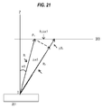
- FIG. 21 shows a detailed view of these features.
- R 2 is the radius vector to the light ray exiting the outside surface 206 of the short throw lens 200 at point P 2 , while ⁇ 2 represents the angle that that ray makes with respect to the vertical optical axis Z, and ⁇ R 2 is the incremental change in R 2 as ⁇ 2 increases incrementally ( ⁇ 2 ).
- R 2 monotonically increases as ⁇ 2 , increases in a range of 0 to 60°.
- the toroidal portion of the outside surface 206 is axisymmetrical with respect to the vertical optical axis Z.
- the short throw lens 200 In order to avoid total internal reflection of light emitted from the light source 201 into the short throw lens 200 , A 2 ⁇ 1/ ⁇ (n 2 ⁇ 1), where n is a refraction index of a material forming the illumination lens, and A 2 ⁇ R 2 /(R 2 ⁇ 2 ).
- the short throw lens 200 is made of a transparent material having an index of refraction between 1.41 and 1.65.
- the painted bottom surface 208 of the short throw lens 200 may be configured to absorb internal (e.g., Fresnel) reflection of light emitted by the light source 201 .
- the bottom surface 208 may be painted such that the absorptivity of the bottom surface 208 is at least 80%, and preferably 90%.
- the bottom surface 208 of the short throw lens 200 may be painted with a black paint in order to increase absorptivity.
- the top of a printed circuit board on which the short throw lens 200 may be mounted can be similarly painted in order to increase absorptivity.
- the lens size of the lens is a free parameter, but etendue considerations dictate that a price be paid for a lens that is too small.
- the output beam will be inescapably wider than the goal if the lens is too small.
- the result will be an inability to maintain an output illumination pattern that is the ideal linear ramp of curve 103 of FIG. 10 , because it requires the source image of curve 106 . If the lens is smaller than the required source image size, then it cannot supply the required illumination. Thus the lens size will be a parameter fixed by the goal of a linear ramp. Lenses that are too small will have some rays trapped by total internal reflection instead of going to the edge of the pattern. If this is encountered in the design process then the iteration will have to re-start with a greater height of the lens-center above the LED.
- LED illumination lenses may need a circularly symmetric illumination lens that can be used in small numbers (such as five or six per mullion) and still attain uniformity, because the individual patterns are such that those few may add up to caustic-free uniformity.
- an objective of the present invention is to provide a lens with a circular illumination pattern that multiples of which will add up to uniformity across a rectangle. It is a further objective of the present invention to attain a smaller lens size than the above mentioned approaches, leading to device compactness that results in lower manufacturing cost.
- the smaller lens size can be achieved by a specific tailoring of its individual illumination pattern.
- This pattern is an optimal annulus with a specific fall-off that enables the twelve patterns to add up to uniformity between the two illuminating mullions upon which each row of six illuminators are mounted. This fall-off at the most oblique directions is important, because this is what determines overall lens size.
- the alternative approaches are: (1) Each mullion illuminates 100% to mid-shelf and zero beyond, which leads to the aforementioned caustics; (2) Each mullion contributes 50% at the mid-point, falling off beyond it. The latter is the approach of the present invention.
- the exemplary embodiments disclosed herein fulfill a most challenging illumination task, the uniform illumination of close planar targets by widely spaced lenses. Deviations from this lens shape that are not visible to casual inspection may nevertheless suffice to produce detractive visual artifacts in the output pattern. Experienced molders know that sometimes it is necessary to measure the shape of the lenses to a nearly microscopic degree, so as to adjust the mold-parameters until the proper shape is achieved.
Landscapes
- Engineering & Computer Science (AREA)
- Physics & Mathematics (AREA)
- General Engineering & Computer Science (AREA)
- Optics & Photonics (AREA)
- General Physics & Mathematics (AREA)
- Microelectronics & Electronic Packaging (AREA)
- Thermal Sciences (AREA)
- Mechanical Engineering (AREA)
- Combustion & Propulsion (AREA)
- Chemical & Material Sciences (AREA)
- Led Device Packages (AREA)
- Lenses (AREA)
- Securing Globes, Refractors, Reflectors Or The Like (AREA)
- Fastening Of Light Sources Or Lamp Holders (AREA)
- Arrangement Of Elements, Cooling, Sealing, Or The Like Of Lighting Devices (AREA)
- Planar Illumination Modules (AREA)
Priority Applications (4)
| Application Number | Priority Date | Filing Date | Title |
|---|---|---|---|
| US13/785,682 US8992053B2 (en) | 2012-03-05 | 2013-03-05 | Illumination lens for short-throw lighting |
| US14/639,526 US9714751B2 (en) | 2012-03-05 | 2015-03-05 | Illumination lens for short-throw lighting |
| US14/672,530 US9631790B2 (en) | 2012-03-05 | 2015-03-30 | Illumination lens for short-throw lighting |
| US14/813,937 US9664356B2 (en) | 2012-03-05 | 2015-07-30 | Illumination lens for short-throw lighting |
Applications Claiming Priority (2)
| Application Number | Priority Date | Filing Date | Title |
|---|---|---|---|
| US201261606710P | 2012-03-05 | 2012-03-05 | |
| US13/785,682 US8992053B2 (en) | 2012-03-05 | 2013-03-05 | Illumination lens for short-throw lighting |
Related Child Applications (1)
| Application Number | Title | Priority Date | Filing Date |
|---|---|---|---|
| US14/639,526 Continuation US9714751B2 (en) | 2012-03-05 | 2015-03-05 | Illumination lens for short-throw lighting |
Publications (2)
| Publication Number | Publication Date |
|---|---|
| US20130229810A1 US20130229810A1 (en) | 2013-09-05 |
| US8992053B2 true US8992053B2 (en) | 2015-03-31 |
Family
ID=49042747
Family Applications (4)
| Application Number | Title | Priority Date | Filing Date |
|---|---|---|---|
| US13/785,682 Active 2033-03-31 US8992053B2 (en) | 2012-03-05 | 2013-03-05 | Illumination lens for short-throw lighting |
| US14/639,526 Active 2033-05-19 US9714751B2 (en) | 2012-03-05 | 2015-03-05 | Illumination lens for short-throw lighting |
| US14/672,530 Active 2033-08-25 US9631790B2 (en) | 2012-03-05 | 2015-03-30 | Illumination lens for short-throw lighting |
| US14/813,937 Active US9664356B2 (en) | 2012-03-05 | 2015-07-30 | Illumination lens for short-throw lighting |
Family Applications After (3)
| Application Number | Title | Priority Date | Filing Date |
|---|---|---|---|
| US14/639,526 Active 2033-05-19 US9714751B2 (en) | 2012-03-05 | 2015-03-05 | Illumination lens for short-throw lighting |
| US14/672,530 Active 2033-08-25 US9631790B2 (en) | 2012-03-05 | 2015-03-30 | Illumination lens for short-throw lighting |
| US14/813,937 Active US9664356B2 (en) | 2012-03-05 | 2015-07-30 | Illumination lens for short-throw lighting |
Country Status (6)
| Country | Link |
|---|---|
| US (4) | US8992053B2 (enExample) |
| JP (2) | JP2015517199A (enExample) |
| KR (1) | KR20140137358A (enExample) |
| CN (2) | CN108386740B (enExample) |
| DE (2) | DE212013000079U1 (enExample) |
| WO (1) | WO2013132313A2 (enExample) |
Cited By (3)
| Publication number | Priority date | Publication date | Assignee | Title |
|---|---|---|---|---|
| US20160195247A1 (en) * | 2013-07-23 | 2016-07-07 | Zumtobel Lighting Gmbh | Led illumination module |
| US20170059120A1 (en) * | 2015-08-28 | 2017-03-02 | Panasonic Intellectual Property Management Co., Ltd. | Led module and light fixture with the same |
| US11982440B1 (en) * | 2023-06-09 | 2024-05-14 | Dialight Corporation | Lens to produce wide angle light output in high density LED arrays |
Families Citing this family (53)
| Publication number | Priority date | Publication date | Assignee | Title |
|---|---|---|---|---|
| US9020641B2 (en) * | 2012-06-07 | 2015-04-28 | Samsung Electronics Co., Ltd. | Obstacle sensing module and cleaning robot including the same |
| KR102024291B1 (ko) | 2012-12-18 | 2019-09-23 | 엘지이노텍 주식회사 | 램프 유닛 및 그를 이용한 차량 램프 장치 |
| US9690029B2 (en) | 2013-01-30 | 2017-06-27 | Cree, Inc. | Optical waveguides and luminaires incorporating same |
| US9625638B2 (en) | 2013-03-15 | 2017-04-18 | Cree, Inc. | Optical waveguide body |
| US9366396B2 (en) | 2013-01-30 | 2016-06-14 | Cree, Inc. | Optical waveguide and lamp including same |
| US9869432B2 (en) | 2013-01-30 | 2018-01-16 | Cree, Inc. | Luminaires using waveguide bodies and optical elements |
| US9442243B2 (en) | 2013-01-30 | 2016-09-13 | Cree, Inc. | Waveguide bodies including redirection features and methods of producing same |
| US9581751B2 (en) | 2013-01-30 | 2017-02-28 | Cree, Inc. | Optical waveguide and lamp including same |
| US9291320B2 (en) | 2013-01-30 | 2016-03-22 | Cree, Inc. | Consolidated troffer |
| US9366799B2 (en) | 2013-03-15 | 2016-06-14 | Cree, Inc. | Optical waveguide bodies and luminaires utilizing same |
| US10209429B2 (en) | 2013-03-15 | 2019-02-19 | Cree, Inc. | Luminaire with selectable luminous intensity pattern |
| US9798072B2 (en) | 2013-03-15 | 2017-10-24 | Cree, Inc. | Optical element and method of forming an optical element |
| US9920901B2 (en) | 2013-03-15 | 2018-03-20 | Cree, Inc. | LED lensing arrangement |
| US10400984B2 (en) | 2013-03-15 | 2019-09-03 | Cree, Inc. | LED light fixture and unitary optic member therefor |
| US10502899B2 (en) * | 2013-03-15 | 2019-12-10 | Ideal Industries Lighting Llc | Outdoor and/or enclosed structure LED luminaire |
| US10436970B2 (en) | 2013-03-15 | 2019-10-08 | Ideal Industries Lighting Llc | Shaped optical waveguide bodies |
| US10379278B2 (en) * | 2013-03-15 | 2019-08-13 | Ideal Industries Lighting Llc | Outdoor and/or enclosed structure LED luminaire outdoor and/or enclosed structure LED luminaire having outward illumination |
| CN104235754B (zh) * | 2013-06-20 | 2019-06-18 | 欧司朗有限公司 | 用于照明装置的透镜和具有该透镜的照明装置 |
| US9233510B2 (en) * | 2013-07-22 | 2016-01-12 | GE Lighting Solutions, LLC | Lenses for cosine cubed, typical batwing, flat batwing distributions |
| DE102013226181B4 (de) * | 2013-12-17 | 2021-01-28 | Zumtobel Lighting Gmbh | Optisches Element, sowie Anordnung zur Lichtabgabe |
| US12372219B2 (en) * | 2014-05-30 | 2025-07-29 | Cree Lighting Usa Llc | LED luminaire with a cavity, finned interior, and a curved outer wall extending from a surface on which the light source is mounted |
| KR102423383B1 (ko) * | 2014-12-29 | 2022-07-22 | 엘지이노텍 주식회사 | 조명 장치 |
| TWI711787B (zh) | 2015-01-08 | 2020-12-01 | 韓商Lg伊諾特股份有限公司 | 光學透鏡及具有光學透鏡之發光模組 |
| US10801696B2 (en) | 2015-02-09 | 2020-10-13 | Ecosense Lighting Inc. | Lighting systems generating partially-collimated light emissions |
| US11306897B2 (en) | 2015-02-09 | 2022-04-19 | Ecosense Lighting Inc. | Lighting systems generating partially-collimated light emissions |
| US9869450B2 (en) | 2015-02-09 | 2018-01-16 | Ecosense Lighting Inc. | Lighting systems having a truncated parabolic- or hyperbolic-conical light reflector, or a total internal reflection lens; and having another light reflector |
| JP6470606B2 (ja) * | 2015-03-27 | 2019-02-13 | 株式会社エンプラス | 発光装置、面光源装置および表示装置 |
| USD779112S1 (en) | 2015-04-24 | 2017-02-14 | Abl Ip Holding Llc | Tri-lobe light fixture optic |
| US10393341B2 (en) | 2015-04-24 | 2019-08-27 | Abl Ip Holding Llc | Tri-lobe optic and associated light fixtures |
| WO2016196039A1 (en) * | 2015-06-01 | 2016-12-08 | Koninklijke Philips N.V. | Lens with elongated radiation pattern |
| TWI583031B (zh) * | 2015-06-05 | 2017-05-11 | 一品光學工業股份有限公司 | 光源模組與透鏡 |
| WO2017003090A1 (ko) | 2015-06-30 | 2017-01-05 | 서울바이오시스 주식회사 | Uv led가 적용된 포충기 |
| KR102302586B1 (ko) * | 2015-07-28 | 2021-09-14 | 엘지디스플레이 주식회사 | 광학산 렌즈 및 그를 포함하는 백라이트 유닛과 표시장치 |
| US10495284B2 (en) | 2015-09-08 | 2019-12-03 | Lg Innotek Co., Ltd. | Lens and light emitting unit including same |
| US11137582B2 (en) | 2015-12-28 | 2021-10-05 | Spere Optics Company, Llc | Omnidirectional catadioptric lens with odd aspheric contour or multi-lens |
| JP6417352B2 (ja) | 2016-03-22 | 2018-11-07 | 矢崎総業株式会社 | バックライトユニットおよびヘッドアップディスプレイ装置 |
| US11719882B2 (en) | 2016-05-06 | 2023-08-08 | Ideal Industries Lighting Llc | Waveguide-based light sources with dynamic beam shaping |
| US10416377B2 (en) | 2016-05-06 | 2019-09-17 | Cree, Inc. | Luminaire with controllable light emission |
| US10578278B2 (en) * | 2017-06-05 | 2020-03-03 | Lumileds Holding B.V. | Optical lens for extremely thin direct-lit backlight |
| JP6832543B2 (ja) * | 2017-07-10 | 2021-02-24 | パナソニックIpマネジメント株式会社 | 庫内照明装置 |
| KR102435569B1 (ko) * | 2017-07-12 | 2022-08-23 | 쑤저우 레킨 세미컨덕터 컴퍼니 리미티드 | 광학 렌즈, 조명 모듈 및 이를 구비한 라이트 유닛 |
| US10851967B2 (en) | 2017-11-17 | 2020-12-01 | Osram Gmbh | Lens, corresponding lighting device, lighting installation and method |
| DE102018132611A1 (de) * | 2018-09-27 | 2020-04-02 | Liebherr-Hausgeräte Ochsenhausen GmbH | Kühl- und/oder Gefriergerät |
| CN110347051A (zh) * | 2019-07-19 | 2019-10-18 | 深圳创维-Rgb电子有限公司 | 红外发射机构、红外遥控设备及红外控制的智慧家庭系统 |
| KR102129706B1 (ko) * | 2019-08-13 | 2020-07-03 | 주식회사 옵토전자 | 마이크로 광학소자 및 이를 포함하는 광전자 모듈 |
| JP2021113882A (ja) * | 2020-01-17 | 2021-08-05 | 株式会社東海理化電機製作所 | レンズ及びライセンスランプ |
| EP3861892B1 (de) | 2020-02-04 | 2023-12-06 | Lumitech Patentverwertung GmbH | Leuchte zum ausleuchten von regalmöbeln und regalmöbel mit einer leuchte |
| EP4136490A1 (en) * | 2020-04-15 | 2023-02-22 | CommScope Connectivity Belgium BV | Device and method for sealing cables in telecommunications enclosures |
| CN111830485B (zh) * | 2020-07-01 | 2025-04-04 | 东莞市美光达光学科技有限公司 | 一种用于广角飞行时间光学测距的红外发射模块及其模组 |
| KR102863462B1 (ko) | 2020-10-15 | 2025-09-22 | 에이엠에스-오스람 아시아 퍼시픽 피티이. 리미티드 | 확장된 조명 필드를 갖는 투영 |
| JP7315858B2 (ja) * | 2021-02-17 | 2023-07-27 | 日亜化学工業株式会社 | 発光装置 |
| CN114899295B (zh) * | 2022-05-18 | 2025-10-14 | 深圳循光科技有限公司 | 一种半导体发光单元和半导体发光器件 |
| CN115899614B (zh) * | 2022-11-09 | 2025-10-31 | 上海天马微电子有限公司 | 导光板组件、背光模组及显示装置 |
Citations (15)
| Publication number | Priority date | Publication date | Assignee | Title |
|---|---|---|---|---|
| US20040095778A1 (en) * | 2002-11-15 | 2004-05-20 | Zynda Dennis R. | Device for illuminating transmission shifter knobs |
| US20050195603A1 (en) * | 2001-10-18 | 2005-09-08 | Ilight Technologies, Inc. | Color-changing illumination device |
| US20060138437A1 (en) | 2004-12-29 | 2006-06-29 | Tien-Fu Huang | Lens and LED using the lens to achieve homogeneous illumination |
| US20070091615A1 (en) * | 2005-10-25 | 2007-04-26 | Chi-Tang Hsieh | Backlight module for LCD monitors and method of backlighting the same |
| US7273299B2 (en) | 2005-01-26 | 2007-09-25 | Pelka & Associates | Cylindrical irradiance-mapping lens and its applications to LED shelf-lighting |
| US7348723B2 (en) | 2004-09-27 | 2008-03-25 | Enplas Corporation | Emission device, surface light source device, display and light flux control member |
| US7445370B2 (en) | 2004-07-16 | 2008-11-04 | Enplas Corporation | Surface light source device, illumination unit and light flux control member |
| US20080278944A1 (en) | 2005-04-06 | 2008-11-13 | Ju-Young Yoon | Optical lens, optical module having the same, and backlight assembly having the same |
| EP2023038A2 (en) | 2007-08-09 | 2009-02-11 | Sharp Kabushiki Kaisha | LED diffusion lens for LCD backlighting. |
| US7621657B2 (en) | 2006-01-24 | 2009-11-24 | Enplas Corporation | Light emitting device, surface light source device, display and light flux control member |
| US7654702B1 (en) * | 2008-08-25 | 2010-02-02 | Fu Zhun Precision (Shen Zhen) Co., Ltd. | LED lamp |
| US7674019B2 (en) | 2007-08-11 | 2010-03-09 | Anthony, Inc. | Free-form lenses for rectangular illumination zones |
| US7731395B2 (en) | 2005-01-26 | 2010-06-08 | Anthony International | Linear lenses for LEDs |
| US20110141734A1 (en) * | 2009-12-11 | 2011-06-16 | Osram Sylvania Inc. | Lens generating a batwing-shaped beam distribution, and method therefor |
| US20120014115A1 (en) | 2010-01-07 | 2012-01-19 | Seoul Semiconductor Co., Ltd. | Aspherical led lens and light emitting device including the same |
Family Cites Families (8)
| Publication number | Priority date | Publication date | Assignee | Title |
|---|---|---|---|---|
| CN2054539U (zh) * | 1989-01-31 | 1990-03-14 | 中国科学院安徽光学精密机械研究所 | 光吸收器 |
| JP2001315380A (ja) * | 2000-05-10 | 2001-11-13 | Canon Inc | ロッドレンズアレイ及びそれを用いた画像形成装置 |
| JP4299535B2 (ja) * | 2002-12-16 | 2009-07-22 | パナソニック株式会社 | 発光ダイオード表示装置 |
| JP4357508B2 (ja) * | 2006-07-28 | 2009-11-04 | 株式会社エンプラス | 発光装置、面光源装置、表示装置及び光束制御部材 |
| JP4350144B2 (ja) * | 2007-08-09 | 2009-10-21 | シャープ株式会社 | 発光装置およびこれを備える照明装置 |
| JP4479805B2 (ja) * | 2008-02-15 | 2010-06-09 | ソニー株式会社 | レンズ、光源ユニット、バックライト装置及び表示装置 |
| CN101561085A (zh) * | 2009-05-14 | 2009-10-21 | 上海广电光电子有限公司 | 广角led光源 |
| CN101986018B (zh) * | 2010-11-03 | 2012-05-02 | 吴峰 | 宽配光角led路灯透镜单元及模块 |
-
2013
- 2013-03-05 WO PCT/IB2013/000460 patent/WO2013132313A2/en not_active Ceased
- 2013-03-05 CN CN201810153841.4A patent/CN108386740B/zh active Active
- 2013-03-05 DE DE212013000079.0U patent/DE212013000079U1/de not_active Expired - Lifetime
- 2013-03-05 DE DE112013003456.5T patent/DE112013003456T5/de active Pending
- 2013-03-05 US US13/785,682 patent/US8992053B2/en active Active
- 2013-03-05 JP JP2014560453A patent/JP2015517199A/ja not_active Withdrawn
- 2013-03-05 KR KR1020147025283A patent/KR20140137358A/ko not_active Ceased
- 2013-03-05 CN CN201380013036.7A patent/CN104254733B/zh active Active
-
2015
- 2015-03-05 US US14/639,526 patent/US9714751B2/en active Active
- 2015-03-30 US US14/672,530 patent/US9631790B2/en active Active
- 2015-07-30 US US14/813,937 patent/US9664356B2/en active Active
-
2018
- 2018-02-14 JP JP2018024542A patent/JP2018125535A/ja not_active Withdrawn
Patent Citations (16)
| Publication number | Priority date | Publication date | Assignee | Title |
|---|---|---|---|---|
| US20050195603A1 (en) * | 2001-10-18 | 2005-09-08 | Ilight Technologies, Inc. | Color-changing illumination device |
| US20040095778A1 (en) * | 2002-11-15 | 2004-05-20 | Zynda Dennis R. | Device for illuminating transmission shifter knobs |
| US7445370B2 (en) | 2004-07-16 | 2008-11-04 | Enplas Corporation | Surface light source device, illumination unit and light flux control member |
| US7348723B2 (en) | 2004-09-27 | 2008-03-25 | Enplas Corporation | Emission device, surface light source device, display and light flux control member |
| US20060138437A1 (en) | 2004-12-29 | 2006-06-29 | Tien-Fu Huang | Lens and LED using the lens to achieve homogeneous illumination |
| US7731395B2 (en) | 2005-01-26 | 2010-06-08 | Anthony International | Linear lenses for LEDs |
| US7273299B2 (en) | 2005-01-26 | 2007-09-25 | Pelka & Associates | Cylindrical irradiance-mapping lens and its applications to LED shelf-lighting |
| US20080278944A1 (en) | 2005-04-06 | 2008-11-13 | Ju-Young Yoon | Optical lens, optical module having the same, and backlight assembly having the same |
| US20070091615A1 (en) * | 2005-10-25 | 2007-04-26 | Chi-Tang Hsieh | Backlight module for LCD monitors and method of backlighting the same |
| US7621657B2 (en) | 2006-01-24 | 2009-11-24 | Enplas Corporation | Light emitting device, surface light source device, display and light flux control member |
| EP2023038A2 (en) | 2007-08-09 | 2009-02-11 | Sharp Kabushiki Kaisha | LED diffusion lens for LCD backlighting. |
| US7798679B2 (en) | 2007-08-09 | 2010-09-21 | Sharp Kabushiki Kaisha | Light emitting device and lighting device having the same |
| US7674019B2 (en) | 2007-08-11 | 2010-03-09 | Anthony, Inc. | Free-form lenses for rectangular illumination zones |
| US7654702B1 (en) * | 2008-08-25 | 2010-02-02 | Fu Zhun Precision (Shen Zhen) Co., Ltd. | LED lamp |
| US20110141734A1 (en) * | 2009-12-11 | 2011-06-16 | Osram Sylvania Inc. | Lens generating a batwing-shaped beam distribution, and method therefor |
| US20120014115A1 (en) | 2010-01-07 | 2012-01-19 | Seoul Semiconductor Co., Ltd. | Aspherical led lens and light emitting device including the same |
Non-Patent Citations (2)
| Title |
|---|
| International Search Report issued on Sep. 25, 2013 in International Application No. PCT/IB2013/000460. |
| IWritten Opinion issued on Sep. 25, 2013 in International Application No. PCT/IB2013/000460. |
Cited By (4)
| Publication number | Priority date | Publication date | Assignee | Title |
|---|---|---|---|---|
| US20160195247A1 (en) * | 2013-07-23 | 2016-07-07 | Zumtobel Lighting Gmbh | Led illumination module |
| US20170059120A1 (en) * | 2015-08-28 | 2017-03-02 | Panasonic Intellectual Property Management Co., Ltd. | Led module and light fixture with the same |
| US9964283B2 (en) * | 2015-08-28 | 2018-05-08 | Panasonic Intellectual Property Management Co., Ltd. | LED module having a lens with a hollow and light fixture with the same |
| US11982440B1 (en) * | 2023-06-09 | 2024-05-14 | Dialight Corporation | Lens to produce wide angle light output in high density LED arrays |
Also Published As
| Publication number | Publication date |
|---|---|
| JP2018125535A (ja) | 2018-08-09 |
| WO2013132313A3 (en) | 2013-12-12 |
| CN108386740B (zh) | 2020-05-26 |
| US9714751B2 (en) | 2017-07-25 |
| KR20140137358A (ko) | 2014-12-02 |
| US20150176776A1 (en) | 2015-06-25 |
| US9631790B2 (en) | 2017-04-25 |
| US20150338056A1 (en) | 2015-11-26 |
| DE112013003456T5 (de) | 2015-05-07 |
| US20150204509A1 (en) | 2015-07-23 |
| DE212013000079U1 (de) | 2014-10-28 |
| WO2013132313A2 (en) | 2013-09-12 |
| CN104254733B (zh) | 2018-03-27 |
| US9664356B2 (en) | 2017-05-30 |
| CN108386740A (zh) | 2018-08-10 |
| CN104254733A (zh) | 2014-12-31 |
| JP2015517199A (ja) | 2015-06-18 |
| US20130229810A1 (en) | 2013-09-05 |
Similar Documents
| Publication | Publication Date | Title |
|---|---|---|
| US9714751B2 (en) | Illumination lens for short-throw lighting | |
| US9046293B2 (en) | Wide-angle non-imaging illumination lens arrayable for close planar targets | |
| US20120268950A1 (en) | Wide-Angle Non-Imaging Illumination Lens Arrayable for Close Planar Targets | |
| US9880417B2 (en) | Illumination lens for LED backlights | |
| US8967833B2 (en) | LED lens and light source device using the same | |
| US5577493A (en) | Auxiliary lens to modify the output flux distribution of a TIR lens | |
| JP5336474B2 (ja) | 半鏡面構成要素を備えたリサイクル型バックライト | |
| CN105546475B (zh) | 波长混合光学部件 | |
| KR101299529B1 (ko) | 발광다이오드용 렌즈, 이를 구비하는 백라이트유닛 및 표시장치 | |
| WO2013022109A1 (en) | Backlight | |
| US10983394B2 (en) | Thin direct-view LED backlights | |
| CN100420050C (zh) | 发光光源及其发光光源阵列 | |
| US8162501B2 (en) | Display device having high brightness uniformity at positions close to light source | |
| KR20150094550A (ko) | 측면 방출형 엘이디 렌즈 | |
| JP3169586U (ja) | 集光レンズモジュール | |
| JP5243590B2 (ja) | 平面照明装置ユニット |
Legal Events
| Date | Code | Title | Description |
|---|---|---|---|
| AS | Assignment |
Owner name: SEOUL SEMICONDUCTOR CO., LTD., KOREA, REPUBLIC OF Free format text: ASSIGNMENT OF ASSIGNORS INTEREST;ASSIGNOR:PELKA, DAVID G;REEL/FRAME:034119/0021 Effective date: 20141103 |
|
| FEPP | Fee payment procedure |
Free format text: PAYOR NUMBER ASSIGNED (ORIGINAL EVENT CODE: ASPN); ENTITY STATUS OF PATENT OWNER: LARGE ENTITY |
|
| STCF | Information on status: patent grant |
Free format text: PATENTED CASE |
|
| MAFP | Maintenance fee payment |
Free format text: PAYMENT OF MAINTENANCE FEE, 4TH YEAR, LARGE ENTITY (ORIGINAL EVENT CODE: M1551) Year of fee payment: 4 |
|
| MAFP | Maintenance fee payment |
Free format text: PAYMENT OF MAINTENANCE FEE, 8TH YEAR, LARGE ENTITY (ORIGINAL EVENT CODE: M1552); ENTITY STATUS OF PATENT OWNER: LARGE ENTITY Year of fee payment: 8 |