US8968889B2 - Organic compound and organic light-emitting device - Google Patents

Organic compound and organic light-emitting device Download PDF

Info

Publication number
US8968889B2
US8968889B2 US13/634,372 US201113634372A US8968889B2 US 8968889 B2 US8968889 B2 US 8968889B2 US 201113634372 A US201113634372 A US 201113634372A US 8968889 B2 US8968889 B2 US 8968889B2
Authority
US
United States
Prior art keywords
group
emitting device
organic compound
light
organic
Prior art date
Legal status (The legal status is an assumption and is not a legal conclusion. Google has not performed a legal analysis and makes no representation as to the accuracy of the status listed.)
Active, expires
Application number
US13/634,372
Other versions
US20130002526A1 (en
Inventor
Jun Kamatani
Kengo Kishino
Naoki Yamada
Akihito Saitoh
Current Assignee (The listed assignees may be inaccurate. Google has not performed a legal analysis and makes no representation or warranty as to the accuracy of the list.)
Canon Inc
Original Assignee
Canon Inc
Priority date (The priority date is an assumption and is not a legal conclusion. Google has not performed a legal analysis and makes no representation as to the accuracy of the date listed.)
Filing date
Publication date
Application filed by Canon Inc filed Critical Canon Inc
Assigned to CANON KABUSHIKI KAISHA reassignment CANON KABUSHIKI KAISHA ASSIGNMENT OF ASSIGNORS INTEREST (SEE DOCUMENT FOR DETAILS). Assignors: KAMATANI, JUN, KISHINO, KENGO, SAITOH, AKIHITO, YAMADA, NAOKI
Publication of US20130002526A1 publication Critical patent/US20130002526A1/en
Application granted granted Critical
Publication of US8968889B2 publication Critical patent/US8968889B2/en
Active legal-status Critical Current
Adjusted expiration legal-status Critical

Links

Images

Classifications

    • CCHEMISTRY; METALLURGY
    • C07ORGANIC CHEMISTRY
    • C07DHETEROCYCLIC COMPOUNDS
    • C07D471/00Heterocyclic compounds containing nitrogen atoms as the only ring hetero atoms in the condensed system, at least one ring being a six-membered ring with one nitrogen atom, not provided for by groups C07D451/00 - C07D463/00
    • C07D471/02Heterocyclic compounds containing nitrogen atoms as the only ring hetero atoms in the condensed system, at least one ring being a six-membered ring with one nitrogen atom, not provided for by groups C07D451/00 - C07D463/00 in which the condensed system contains two hetero rings
    • C07D471/04Ortho-condensed systems
    • CCHEMISTRY; METALLURGY
    • C07ORGANIC CHEMISTRY
    • C07CACYCLIC OR CARBOCYCLIC COMPOUNDS
    • C07C13/00Cyclic hydrocarbons containing rings other than, or in addition to, six-membered aromatic rings
    • C07C13/28Polycyclic hydrocarbons or acyclic hydrocarbon derivatives thereof
    • C07C13/32Polycyclic hydrocarbons or acyclic hydrocarbon derivatives thereof with condensed rings
    • C07C13/62Polycyclic hydrocarbons or acyclic hydrocarbon derivatives thereof with condensed rings with more than three condensed rings
    • CCHEMISTRY; METALLURGY
    • C07ORGANIC CHEMISTRY
    • C07DHETEROCYCLIC COMPOUNDS
    • C07D209/00Heterocyclic compounds containing five-membered rings, condensed with other rings, with one nitrogen atom as the only ring hetero atom
    • C07D209/56Ring systems containing three or more rings
    • C07D209/80[b, c]- or [b, d]-condensed
    • C07D209/82Carbazoles; Hydrogenated carbazoles
    • C07D209/86Carbazoles; Hydrogenated carbazoles with only hydrogen atoms, hydrocarbon or substituted hydrocarbon radicals, directly attached to carbon atoms of the ring system
    • CCHEMISTRY; METALLURGY
    • C09DYES; PAINTS; POLISHES; NATURAL RESINS; ADHESIVES; COMPOSITIONS NOT OTHERWISE PROVIDED FOR; APPLICATIONS OF MATERIALS NOT OTHERWISE PROVIDED FOR
    • C09KMATERIALS FOR MISCELLANEOUS APPLICATIONS, NOT PROVIDED FOR ELSEWHERE
    • C09K11/00Luminescent, e.g. electroluminescent, chemiluminescent materials
    • C09K11/06Luminescent, e.g. electroluminescent, chemiluminescent materials containing organic luminescent materials
    • HELECTRICITY
    • H05ELECTRIC TECHNIQUES NOT OTHERWISE PROVIDED FOR
    • H05BELECTRIC HEATING; ELECTRIC LIGHT SOURCES NOT OTHERWISE PROVIDED FOR; CIRCUIT ARRANGEMENTS FOR ELECTRIC LIGHT SOURCES, IN GENERAL
    • H05B33/00Electroluminescent light sources
    • H05B33/12Light sources with substantially two-dimensional radiating surfaces
    • H05B33/14Light sources with substantially two-dimensional radiating surfaces characterised by the chemical or physical composition or the arrangement of the electroluminescent material, or by the simultaneous addition of the electroluminescent material in or onto the light source
    • CCHEMISTRY; METALLURGY
    • C09DYES; PAINTS; POLISHES; NATURAL RESINS; ADHESIVES; COMPOSITIONS NOT OTHERWISE PROVIDED FOR; APPLICATIONS OF MATERIALS NOT OTHERWISE PROVIDED FOR
    • C09KMATERIALS FOR MISCELLANEOUS APPLICATIONS, NOT PROVIDED FOR ELSEWHERE
    • C09K2211/00Chemical nature of organic luminescent or tenebrescent compounds
    • C09K2211/10Non-macromolecular compounds
    • C09K2211/1003Carbocyclic compounds
    • C09K2211/1011Condensed systems
    • H01L51/0057
    • H01L51/0059
    • H01L51/0072
    • H01L51/5012
    • HELECTRICITY
    • H10SEMICONDUCTOR DEVICES; ELECTRIC SOLID-STATE DEVICES NOT OTHERWISE PROVIDED FOR
    • H10KORGANIC ELECTRIC SOLID-STATE DEVICES
    • H10K50/00Organic light-emitting devices
    • H10K50/10OLEDs or polymer light-emitting diodes [PLED]
    • H10K50/11OLEDs or polymer light-emitting diodes [PLED] characterised by the electroluminescent [EL] layers
    • HELECTRICITY
    • H10SEMICONDUCTOR DEVICES; ELECTRIC SOLID-STATE DEVICES NOT OTHERWISE PROVIDED FOR
    • H10KORGANIC ELECTRIC SOLID-STATE DEVICES
    • H10K85/00Organic materials used in the body or electrodes of devices covered by this subclass
    • H10K85/60Organic compounds having low molecular weight
    • H10K85/615Polycyclic condensed aromatic hydrocarbons, e.g. anthracene
    • H10K85/625Polycyclic condensed aromatic hydrocarbons, e.g. anthracene containing at least one aromatic ring having 7 or more carbon atoms, e.g. azulene
    • HELECTRICITY
    • H10SEMICONDUCTOR DEVICES; ELECTRIC SOLID-STATE DEVICES NOT OTHERWISE PROVIDED FOR
    • H10KORGANIC ELECTRIC SOLID-STATE DEVICES
    • H10K85/00Organic materials used in the body or electrodes of devices covered by this subclass
    • H10K85/60Organic compounds having low molecular weight
    • H10K85/631Amine compounds having at least two aryl rest on at least one amine-nitrogen atom, e.g. triphenylamine
    • HELECTRICITY
    • H10SEMICONDUCTOR DEVICES; ELECTRIC SOLID-STATE DEVICES NOT OTHERWISE PROVIDED FOR
    • H10KORGANIC ELECTRIC SOLID-STATE DEVICES
    • H10K85/00Organic materials used in the body or electrodes of devices covered by this subclass
    • H10K85/60Organic compounds having low molecular weight
    • H10K85/649Aromatic compounds comprising a hetero atom
    • H10K85/657Polycyclic condensed heteroaromatic hydrocarbons
    • H10K85/6572Polycyclic condensed heteroaromatic hydrocarbons comprising only nitrogen in the heteroaromatic polycondensed ring system, e.g. phenanthroline or carbazole
    • YGENERAL TAGGING OF NEW TECHNOLOGICAL DEVELOPMENTS; GENERAL TAGGING OF CROSS-SECTIONAL TECHNOLOGIES SPANNING OVER SEVERAL SECTIONS OF THE IPC; TECHNICAL SUBJECTS COVERED BY FORMER USPC CROSS-REFERENCE ART COLLECTIONS [XRACs] AND DIGESTS
    • Y10TECHNICAL SUBJECTS COVERED BY FORMER USPC
    • Y10STECHNICAL SUBJECTS COVERED BY FORMER USPC CROSS-REFERENCE ART COLLECTIONS [XRACs] AND DIGESTS
    • Y10S428/00Stock material or miscellaneous articles
    • Y10S428/917Electroluminescent

Definitions

  • the present invention relates to a novel organic compound and an organic light-emitting device including the same.
  • Organic light-emitting devices are devices including a pair of electrodes and an organic compound layer disposed between the pair of electrodes. By injecting electrons and holes from the electrodes, excitons of an organic compound are generated, and light is emitted when the excitons are returned to the ground state. Such organic light-emitting devices are also referred to as “organic electroluminescent devices” or “organic EL devices.
  • PTL 1 discloses compound IK-17 represented by the structural formula below.
  • Compound IK-17 has a structure having benzo[k]fluoranthene as a basic structure and having a phenyl group at each of the 7-position and the 12-position of the benzo[k]fluoranthene.
  • basic structure means a structure constituted by only a fused-ring structure.
  • Compound IK-17 disclosed in PTL 1 emits blue light. Furthermore, this basic structure emits ultraviolet light, which has a wavelength shorter than that of blue light. It is believed that light having a longer wavelength can be emitted by introducing a substituent into this basic structure. Green light can be emitted by introducing some types of substituents. However, introducing a substituent may impair the stability of the compound.
  • the present invention provides a novel organic compound in which light in the green range can be emitted by the basic structure itself.
  • the present invention provides an organic compound represented by general formula (1) below.
  • R 1 to R 18 are each independently selected from a hydrogen atom, a halogen atom, a substituted or unsubstituted alkyl group, a substituted or unsubstituted alkoxy group, a substituted amino group, a substituted or unsubstituted aryl group, and a substituted or unsubstituted heterocyclic group.
  • FIG. 1 is a schematic cross-sectional view showing organic light-emitting devices and switching devices connected to the organic light-emitting devices.
  • R 1 to R 18 are each independently selected from a hydrogen atom, a halogen atom, a substituted or unsubstituted alkyl group, a substituted or unsubstituted alkoxy group, a substituted amino group, a substituted or unsubstituted aryl group, and a substituted or unsubstituted heterocyclic group.
  • examples of the alkyl group include, but are not limited to, a methyl group, an ethyl group, a n-propyl group, an isopropyl group, a n-butyl group, a tert-butyl group, a sec-butyl group, an octyl group, a 1-adamantyl group, and a 2-adamantyl group.
  • examples of the alkoxy group include, but are not limited to, a methoxy group, an ethoxy group, a propoxy group, a 2-ethyl-octyloxy group, a phenoxy group, a 4-tert-butylphenoxy group, a benzyloxy group, and a thienyloxy group.
  • examples of the amino group include, but are not limited to, an N-methylamino group, an N-ethylamino group, an N,N-dimethylamino group, an N,N-diethylamino group, an N-methyl-N-ethylamino group, an N-benzylamino group, an N-methyl-N-benzylamino group, an N,N-dibenzylamino group, an anilino group, an N,N-diphenylamino group, an N,N-dinaphthylamino group, an N,N-difluorenylamino group, an N-phenyl-N-tolylamino group, an N,N-ditolylamino group, an N-methyl-N-phenylamino group, an N,N-dianisolylamino group, an N-mesityl-N-phenylamino group, an N,N-dimesitylamino
  • examples of the aryl group include, but are not limited to, a phenyl group, a naphthyl group, an indenyl group, a biphenyl group, a terphenyl group, and a fluorenyl group.
  • examples of the heterocyclic group include, but are not limited to, a pyridyl group, an oxazolyl group, an oxadiazolyl group, a thiazolyl group, a thiadiazolyl group, a carbazolyl group, an acridinyl group, and a phenanthrolyl group.
  • the above-mentioned substituent i.e., the alkyl group, the alkoxy group, the amino group, the aryl group, or the heterocyclic group may have a substituent such as an alkyl group, e.g., a methyl group, an ethyl group, or a propyl group; an aralkyl group, e.g., a benzyl group; an aryl group, e.g., a phenyl group or a biphenyl group; a heterocyclic group, e.g., a pyridyl group or a pyrrolyl group; an amino group, e.g., a dimethylamino group, a diethylamino group, a dibenzylamino group, a diphenylamino group, or a ditolylamino group; an alkoxyl group, e.g., a methoxyl group, an alkoxyl group
  • the inventors of the present invention focused on the basic structure itself. More specifically, the inventors of the present invention tried to provide a compound in which an emission wavelength of a molecule composed of only the basic structure falls within a desired emission wavelength range.
  • the desired emission wavelength range is a green range, specifically, 480 nm or more and 530 nm or less.
  • a luminescent material itself have a high quantum yield. In order to achieve this, it is necessary for the luminescent material to satisfy the following conditions:
  • the emission wavelength required for a material suitable for emitting green light in an organic light-emitting device it is important that a solution of the luminescent material have an emission peak in the range of 480 nm or more and 530 nm or less.
  • the organic compound according to the present invention has a fused-ring structure in which conjugation is extended from the 8-position to the 10-position of benzo[k]fluoranthene.
  • This structure leads to a further increase in the transition dipole moment as compared with that of benzo[k]fluoranthene.
  • the organic compound according to the present invention has a structure with a high oscillator strength.
  • An organic compound of the present invention will be compared with benzo[k]fluoranthene, which is an analogous compound.
  • the wavelength at which the intensity of a spectrum becomes maximum was compared between 7,12-diphenylbenzo[k]fluoranthene in which each of the 7-position and the 12-position of benzo[k]fluoranthene is substituted with a phenyl group and compound 1 which is an organic compound according to the present invention.
  • the spectrum of the former compound had a maximum intensity at 428 nm. This does not correspond to light emission in the green range.
  • the spectrum of compound 1 had a maximum intensity at 488 nm. Thus, compound 1 emits light in the green range.
  • the organic compound according to the present invention has two five-membered ring structures in the basic structure thereof, the energy levels of the highest occupied molecular orbital (HOMO) and lowest unoccupied molecular orbital (LUMO) are lower (deeper with respect to the vacuum level) than those of compounds having one five-membered ring structure.
  • An organic compound having a low oxidation potential requires larger energy to be oxidized, and thus such a compound is stable against oxidation.
  • the organic compound according to the present invention is used as a luminescent material, the organic compound is suitable as an electron-trapping luminescent material.
  • the electron-trapping luminescent material refers to a luminescent material in which the LUMO level of a luminescent material that performs main light emission is lower than the LUMO level of a material of a layer adjacent to the cathode side of a light-emitting layer. In this case, deficiency of electrons in the luminescent material that performs main light emission can be suppressed.
  • the basic structure of the organic compound according to the present invention contains no heteroatom such as a nitrogen atom. This also contributes to a low oxidation potential. That is, this also contributes to the stability of the organic compound against oxidation. It is also preferable that the substituents of the organic compound contain no heteroatom.
  • the basic structure of the organic compound according to the present invention has a low HOMO energy level. That is, the LUMO energy level of the basic structure is also low. When the LUMO energy level is low, the injection barrier of electrons from the cathode is small, and thus electrons are easily injected.
  • the organic compound according to the present invention is used as a guest material or a host material of a light-emitting layer.
  • the organic compound according to the present invention may be used in any layer other than the light-emitting layer, namely, a hole injection layer, a hole-transporting layer, a hole/exciton-blocking layer, an electron-transporting layer, or an electron injection layer.
  • the organic compound according to the present invention can be preferably used as a guest material of a light-emitting layer of an organic light-emitting device.
  • the organic compound is preferably used as a guest material of a green-light-emitting device.
  • a red-light-emitting material By introducing, into the basic structure of the organic compound according to the present invention, a substituent that shifts the emission wavelength to the long-wavelength side, a red-light-emitting material can also be provided. According to such a material having a basic structure into which a substituent that shifts the emission wavelength to the long-wavelength side is introduced, since the material has the basic structure according to the present invention, the material is stable against oxidation. Examples of the substituent that shifts the emission wavelength to the long-wavelength side include aryl groups, heterocyclic groups, and amino groups.
  • the organic compound according to the present invention is used as a guest material of a light-emitting layer, and a host material having an energy level of the LUMO higher than that of this organic compound, in other words, a host material having an energy level of the LUMO closer to the vacuum level is used.
  • a host material having an energy level of the LUMO closer to the vacuum level is used.
  • the basic structure itself has a wide band gap of 2.4 eV. Therefore, the organic compound according to the present invention can also be used as a host material of a yellow-light-emitting layer or a red-light-emitting layer.
  • the light-emitting layer may include one type of compound.
  • the light-emitting layer may include a plurality of compounds such as a host material and a guest material.
  • the term “host material” refers to a material having the highest weight ratio among compounds constituting a light-emitting layer.
  • the term “guest material” refers to a material that has a weight ratio lower than that of the host material and that performs main light emission among the compounds constituting the light-emitting layer.
  • the term “assist material” refers to a material that has a weight ratio lower than that of the host material and assists the light emission of the guest material among the compounds constituting the light-emitting layer.
  • each compound shown in group A consists of only a hydrocarbon.
  • Compounds consisting of only hydrocarbons have low HOMO energy levels. Accordingly, the oxidation potentials are low, which indicates that the organic compounds are stable against oxidation.
  • the compounds shown in group A consisting of only hydrocarbons are preferable because the stability of their molecules is high.
  • R 19 to R 29 are each independently selected from an alkyl group and an aryl group.
  • This alkyl group is an alkyl group having 1 to 4 carbon atoms.
  • the alkyl group is a methyl group, an ethyl group, a n-propyl group, an isopropyl group, a n-butyl group, an isobutyl group, a sec-butyl group, or a tert-butyl group.
  • a tert-butyl group is preferable because the tert-butyl group has an effect of suppressing molecular association by the steric hindrance.
  • This aryl group is a phenyl group, a naphthyl group, or a fluorenyl group. This is because these aryl groups are substituents suitable for shifting the emission wavelength to the long-wavelength side by about several nanometers to 20 nm in controlling the emission wavelength.
  • the aryl group may further have a substituent.
  • the substituent is an alkyl group having 1 to 4 carbon atoms or a phenyl group.
  • the two phenyl groups bonded to the basic structure in general formula (2) are substituents that suppress concentration quenching. When these phenyl groups have substituents, the effect of suppressing concentration quenching is further increased.
  • the oxidation potential of the molecule significantly changes or the intermolecular interaction changes.
  • the wavelength at which the intensity of a spectrum becomes maximum can be shifted to the long-wavelength side. Since the intermolecular interaction changes, in the case where a substituent contains a nitrogen atom, the compound can be used as an electron-transporting layer, a hole-transporting layer, or a light-emitting layer in a concentration of 100%.
  • the oxidation potential of the molecule also significantly changes or the intermolecular interaction changes. In some cases, a change more significantly than the case where a substituent contains a nitrogen atom can be expected. Since the intermolecular interaction changes, in the case where a substituent contains a heteroatom, the compound can be used as an electron-transporting layer, a hole-transporting layer, or a light-emitting layer in a concentration of 100%.
  • Exemplary compounds of group A to group C have been described.
  • the basic structure itself can emit green light.
  • a substituent is introduced into the basic structure of the organic compound according to the present invention, the emission wavelength is shifted from green to the longer wavelength side. More specifically, such a substituted basic structure can emit red light.
  • the application of the organic compound according to the present invention is not limited to a guest material of a light-emitting layer of an organic light-emitting device.
  • the organic compound according to the present invention may be used as a host material of a light-emitting layer of an organic light-emitting device.
  • the organic compound may be used in an electron-transporting layer, an electron injection layer, a hole-transporting layer, a hole injection layer, or a hole-blocking layer, or the like of an organic light-emitting device.
  • the luminescent color emitted by the organic light-emitting device is not limited.
  • the organic compound according to the present invention can also be used as an assist material or a host material of a light-emitting layer of an organic light-emitting device that emits red light.
  • a reaction formula of the synthetic route is shown below.
  • the synthesis can be conducted while a hydrogen atom located at a position to be substituted is substituted with the target substituent.
  • the substituent to be introduced include an alkyl group, a halogen atom, and a phenyl group.
  • Various compounds can be synthesized by changing compounds D1 to D3 in the above reaction formula. Specific examples of the compounds are shown in Table 1 as synthesized compounds. Table 1 also shows compounds D1 to D3 which are starting materials used for obtaining the synthesized compounds.
  • the organic light-emitting device includes a pair of electrodes, namely, an anode and a cathode, and an organic compound layer disposed between the anode and the cathode.
  • This organic compound layer is a device including the organic compound according to the present invention.
  • the organic light-emitting device may include a plurality of organic compound layers.
  • these plurality of layers include a hole injection layer, a hole-transporting layer, a light-emitting layer, a hole-blocking layer, an exciton-blocking layer, an electron transporting layer, and an electron-injection layer. These layers can be appropriately used in combination.
  • the concentration of the guest material to a host material is preferably 0.1% by weight or more and 30% by weight or less, and more preferably 0.5% by weight or more and 10% by weight or less.
  • the inventors of the present invention have conducted various studies and found that a device in which the organic compound according to the present invention is used as a host material or a guest material, in particular, a guest material of a light-emitting layer had an optical output with a high quantum yield and a high luminance, and had high durability.
  • organic light-emitting device besides the organic compound according to the present invention, publicly known low-molecular weight and high-molecular weight hole injection materials, hole-transporting materials, host materials, guest materials, electron injection materials, electron-transporting materials, and the like can also be used in combination according to need.
  • materials used as a hole injection layer or a hole-transporting layer materials having a high hole mobility are preferably used.
  • the low-molecular weight and high-molecular weight materials having a hole injection performance or a hole transport performance include, but are not limited to, triarylamine derivatives, phenylenediamine derivatives, stilbene derivatives, phthalocyanine derivatives, porphyrin derivatives, poly(vinylcarbazole), poly(thiophene), and other electrically conductive polymers.
  • the host materials may be derivatives of the compounds represented by the structural formulae shown in Table 2.
  • Examples of the host materials further include, but are not limited to, fused-ring compounds (such as fluorene derivatives, naphthalene derivatives, anthracene derivatives, pyrene derivatives, carbazole derivatives, quinoxaline derivatives, and quinoline derivatives), organoaluminum complexes such as tris(8-quinolinolato)aluminum, organozinc complexes, triphenylamine derivatives, and polymer derivatives such as poly(fluorene) derivatives and poly(phenylene) derivatives.
  • fused-ring compounds such as fluorene derivatives, naphthalene derivatives, anthracene derivatives, pyrene derivatives, carbazole derivatives, quinoxaline derivatives, and quinoline derivatives
  • organoaluminum complexes such as tris(8-quinolinolato)aluminum
  • the electron injection materials or the electron-transporting materials are selected in consideration of, for example, the balance with the hole mobility of the hole injection materials or the hole-transporting materials.
  • Examples of the materials having an electron injection performance or an electron transport performance include, but are not limited to, oxadiazole derivatives, oxazole derivatives, pyrazine derivatives, triazole derivatives, triazine derivatives, quinoline derivatives, quinoxaline derivatives, phenanthroline derivatives, and organoaluminum complexes.
  • anode materials those having a work function as high as possible are preferable.
  • the anode materials include metal elements such as gold, platinum, silver, copper, nickel, palladium, cobalt, selenium, vanadium, and tungsten; alloys thereof; and metal oxides such as tin oxide, zinc oxide, indium oxide, indium tin oxide (ITO), and indium zinc oxide.
  • electrically conductive polymers such as polyaniline, polypyrrole, and polythiophene may also be used. These electrode materials may be used alone or in combinations of two or more materials.
  • the anode may have a single-layer structure or a multi-layer structure.
  • cathode materials those having a low work function are preferable.
  • the cathode materials include metal elements such as alkali metals, e.g., lithium; alkaline earth metals, e.g., calcium; aluminum; titanium; manganese; silver; lead; and chromium. Alloys combining these metal elements may also be used.
  • metal elements such as alkali metals, e.g., lithium; alkaline earth metals, e.g., calcium; aluminum; titanium; manganese; silver; lead; and chromium. Alloys combining these metal elements may also be used.
  • magnesium-silver, aluminum-lithium, or aluminum-magnesium can be used.
  • Metal oxides such as indium tin oxide (ITO) may also be used. These electrode materials may be used as alone or in combinations of two or more materials.
  • the cathode may have a single-layer structure or a multi-layer structure.
  • a layer containing the organic compound according to the present invention and layers composed of the other organic compounds are formed by the methods described below.
  • each of the layers is formed by a vacuum evaporation method, an ionized evaporation method, a sputtering method, a method using plasma, or a known coating method (for example, spin coating, dipping, a cast method, a Langmuir Blodgett (LB) method, or an ink jet method) after a material is dissolved in a suitable solvent.
  • a vacuum evaporation method for example, spin coating, dipping, a cast method, a Langmuir Blodgett (LB) method, or an ink jet method
  • the material when a layer is formed by, for example, the vacuum evaporation method or the solution coating method, crystallization does not tend to occur, and thus the resulting layer has good stability with time.
  • the material when a layer is formed by the coating method, the material may be used in combination with a suitable binder resin.
  • binder resin examples include, but are not limited to, polyvinylcarbazole resins, polycarbonate resins, polyester resins, acrylonitrile butadiene styrene (ABS) resins, acrylic resins, polyimide resins, phenolic resins, epoxy resins, silicone resins, and urea resins. These binder resins may be used alone as a homopolymer or a copolymer or used as a mixture of two or more types of resins. Furthermore, additives such as a known plasticizer, antioxidant, or ultraviolet absorber may be optionally used in combination.
  • ABS acrylonitrile butadiene styrene
  • the organic light-emitting device according to this embodiment can be used in a display apparatus or an illuminating device.
  • the organic light-emitting device according to this embodiment can be used in an exposure light source of an electrophotographic image-forming apparatus or a backlight of a liquid crystal display apparatus.
  • the display apparatus includes a display unit including the organic light-emitting device according to this embodiment.
  • This display unit includes a plurality of pixels.
  • Each of the pixels includes the organic light-emitting device according to this embodiment and a thin-film transistor (TFT) device which is an example of a switching device.
  • TFT thin-film transistor
  • An anode or a cathode of this organic light-emitting device is connected to a drain electrode or a source electrode of the TFT device.
  • the display apparatus can be used as an image display apparatus such as a personal computer (PC).
  • the display apparatus may be an image input apparatus that further includes an image input unit.
  • the image input apparatus includes an image input unit to which information from an area CCD sensor, a linear CCD sensor, a memory card, or the like is input and a display unit configured to display the input information.
  • Such an image input apparatus that further includes an imaging optical system constitutes an image pickup apparatus such as a digital camera.
  • the display unit of such an image pickup apparatus or an ink jet printer may have both an image output function of displaying an image on the basis of image information input from the outside and an input function, as an operation panel, of inputting process information to the image.
  • the display apparatus may be used as a display unit of a multifunction printer.
  • FIG. 1 is a schematic cross-sectional view of a display apparatus including organic light-emitting devices according to this embodiment and TFT devices which are an example of switching devices configured to switch emission/non-emission of the organic light-emitting devices.
  • FIG. 1 shows two pairs of an organic light-emitting device and a TFT device.
  • the display device may further include a transistor configured to control the light-emission luminance.
  • the display apparatus performs a display by turning on or turning off the organic light-emitting devices by driving the switching devices in accordance with information, and transmit the information. The detailed structure of the display apparatus will be described below.
  • the display apparatus shown in FIG. 1 includes a substrate 1 composed of, for example, glass and a moisture-proof film 2 for protecting TFT devices or organic compound layers, the moisture-proof film 2 being disposed on the substrate 1 .
  • Reference numeral 3 indicates a metal gate electrode
  • reference numeral 4 indicates a gate insulating film
  • reference numeral 5 indicates a semiconductor layer.
  • TFT devices 8 each include the semiconductor layer 5 , a drain electrode 6 , and a source electrode 7 .
  • An insulating film 9 is provided on the upper portion of the TFT devices 8 .
  • An anode 11 of an organic light-emitting device is connected to the source electrode 7 through a contact hole 10 .
  • the structure of the display apparatus is not limited to this. It is sufficient that either the anode or the cathode of the organic light-emitting device is connected to either the source electrode or the drain electrode of a TFT device.
  • FIG. 1 a plurality of organic compound layers are shown as a single organic compound layer 12 .
  • a first protective layer 14 and a second protective layer 15 for suppressing degradation of the organic light-emitting devices are provided on a cathode 13 .
  • An emission spectrum of a toluene solution of Exemplary compound A2 with a concentration of 1 ⁇ 10 5 mol/L was obtained by measuring photoluminescence at an excitation wavelength of 350 nm using a fluorescence spectrophotometer F-4500 produced by Hitachi, Ltd. According to the measurement result, the spectrum had a maximum intensity at 487 nm.
  • Exemplary compound A3 was obtained by the same reactions and purification procedures as those performed in Example 1 except that the organic compound E5 used in Example 1 was changed to an organic compound E7.
  • An emission spectrum of a toluene solution of Exemplary compound A3 with a concentration of 1 ⁇ 10 ⁇ 5 mol/L was obtained by measuring photoluminescence at an excitation wavelength of 350 nm using a fluorescence spectrophotometer F-4500 produced by Hitachi, Ltd. According to the measurement result, the spectrum had a maximum intensity at 488 nm.
  • Exemplary compound A4 was obtained by the same reactions and purification procedures as those performed in Example 1 except that the organic compound E5 used in Example 1 was changed to an organic compound E8.
  • An emission spectrum of a toluene solution of Exemplary compound A4 with a concentration of 1 ⁇ 10 ⁇ 5 mol/L was obtained by measuring photoluminescence at an excitation wavelength of 350 nm using a fluorescence spectrophotometer F-4500 produced by Hitachi, Ltd. According to the measurement result, the spectrum had a maximum intensity at 488 nm.
  • Exemplary compound A14 was obtained by the same reactions and purification procedures as those performed in Example 1 except that the organic compound E4 used in Example 1 was changed to an organic compound E9, and that the organic compound E5 used in Example 1 was changed to the organic compound E7.
  • An emission spectrum of a toluene solution of Exemplary compound A14 with a concentration of 1 ⁇ 10 ⁇ 5 mol/L was obtained by measuring photoluminescence at an excitation wavelength of 350 nm using a fluorescence spectrophotometer F-4500 produced by Hitachi, Ltd. According to the measurement result, the spectrum had a maximum intensity at 490 nm.
  • an organic light-emitting device having a structure in which an anode, a hole-transporting layer, a light-emitting layer, a hole/exciton-blocking layer, an electron-transporting layer, and a cathode were sequentially stacked was fabricated.
  • an ITO film having a thickness of 100 nm was patterned on a glass substrate.
  • the following organic layers and electrode layers were successively deposited by a resistance-heating vacuum evaporation method in a vacuum chamber at a pressure of 10 ⁇ 5 Pa so that the area of the facing electrodes was 3 mm 2 .
  • Light-emitting layer (30 nm); Host: G-2, Guest: Exemplary compound (weight ratio 5%)
  • Metal electrode layer 1 (1 nm): LiF
  • Metal electrode layer 2 (100 nm): Al
  • an organic light-emitting device having a structure in which an anode, a hole injection layer, a hole-transporting layer, a light-emitting layer, an electron-transporting layer, and an electron injection layer, and a cathode were sequentially stacked was fabricated.
  • the organic light-emitting device having a resonance structure was fabricated by the method described below.
  • An aluminum alloy (AlNd) film having a thickness of 100 nm and functioning as a reflective anode was deposited on a glass substrate functioning as a support by a sputtering method.
  • an ITO film having a thickness of 80 nm and functioning as a transparent anode was formed by a sputtering method.
  • an element isolation film composed of a polyimide resin and having a thickness of 1.5 micrometers was formed on the periphery of the anode, and an opening having a radius of 3 mm was formed.
  • the substrate was sequentially subjected to ultrasonic washing with acetone and isopropyl alcohol (IPA). The substrate was then washed in boiling IPA, and dried. The surface of this substrate was further subjected to UV cleaning.
  • IPA isopropyl alcohol
  • organic compounds were successively deposited by a resistance-heating vacuum evaporation method in a vacuum chamber at a pressure of 10 ⁇ 5 Pa.
  • indium zinc oxide (IZO) was deposited as a cathode by a sputtering method, thus forming a transparent electrode having a thickness of 30 nm.
  • sealing was performed in a nitrogen atmosphere.
  • the organic light-emitting devices were fabricated.
  • Light-emitting layer 35 nm
  • Host G-13
  • Guest Exemplary compound (weight ratio 2%)
  • Electron injection layer (70 nm): G-15 (weight ratio 80%), Li (weight ratio 20%)
  • the organic compound according to the present invention is a novel compound that has a high quantum yield and that realizes light emission suitable for green light.
  • a light-emitting device having good light-emission characteristics can be fabricated.

Abstract

A novel organic compound suitable for emitting green light and an organic light-emitting device including the organic compound are provided. The organic compound is represented by general formula (1). In general formula (1), R1 to R18 are each independently selected from a hydrogen atom, a halogen atom, a substituted or unsubstituted alkyl group, a substituted or unsubstituted alkoxy group, a substituted amino group, a substituted or unsubstituted aryl group, and a substituted or unsubstituted heterocyclic group.
Figure US08968889-20150303-C00001

Description

TECHNICAL FIELD
The present invention relates to a novel organic compound and an organic light-emitting device including the same.
BACKGROUND ART
Organic light-emitting devices are devices including a pair of electrodes and an organic compound layer disposed between the pair of electrodes. By injecting electrons and holes from the electrodes, excitons of an organic compound are generated, and light is emitted when the excitons are returned to the ground state. Such organic light-emitting devices are also referred to as “organic electroluminescent devices” or “organic EL devices.
Heretofore, novel compounds have been actively developed. For example, as a compound used in a light-emitting layer, PTL 1 discloses compound IK-17 represented by the structural formula below. Compound IK-17 has a structure having benzo[k]fluoranthene as a basic structure and having a phenyl group at each of the 7-position and the 12-position of the benzo[k]fluoranthene. Herein, the term “basic structure” means a structure constituted by only a fused-ring structure.
Figure US08968889-20150303-C00002
CITATION LIST Patent Literature
  • PTL 1: Japanese Patent Laid-Open No. 9-241629 (There is no corresponding foreign case.)
SUMMARY OF INVENTION
Compound IK-17 disclosed in PTL 1 emits blue light. Furthermore, this basic structure emits ultraviolet light, which has a wavelength shorter than that of blue light. It is believed that light having a longer wavelength can be emitted by introducing a substituent into this basic structure. Green light can be emitted by introducing some types of substituents. However, introducing a substituent may impair the stability of the compound.
The present invention provides a novel organic compound in which light in the green range can be emitted by the basic structure itself.
Specifically, the present invention provides an organic compound represented by general formula (1) below.
Figure US08968889-20150303-C00003
In general formula (1), R1 to R18 are each independently selected from a hydrogen atom, a halogen atom, a substituted or unsubstituted alkyl group, a substituted or unsubstituted alkoxy group, a substituted amino group, a substituted or unsubstituted aryl group, and a substituted or unsubstituted heterocyclic group.
According to the present invention, since the basic structure itself has a wide band gap, it is possible to provide an organic compound in which light in the green range can be emitted by the basic structure itself. In addition, an organic light-emitting device including the novel organic compound can be provided.
BRIEF DESCRIPTION OF DRAWINGS
FIG. 1 is a schematic cross-sectional view showing organic light-emitting devices and switching devices connected to the organic light-emitting devices.
DESCRIPTION OF EMBODIMENTS
A novel organic compound according to the present invention is an organic compound represented by general formula (1) below.
Figure US08968889-20150303-C00004
In general formula (1), R1 to R18 are each independently selected from a hydrogen atom, a halogen atom, a substituted or unsubstituted alkyl group, a substituted or unsubstituted alkoxy group, a substituted amino group, a substituted or unsubstituted aryl group, and a substituted or unsubstituted heterocyclic group.
In general formula (1), examples of the alkyl group include, but are not limited to, a methyl group, an ethyl group, a n-propyl group, an isopropyl group, a n-butyl group, a tert-butyl group, a sec-butyl group, an octyl group, a 1-adamantyl group, and a 2-adamantyl group.
In general formula (1), examples of the alkoxy group include, but are not limited to, a methoxy group, an ethoxy group, a propoxy group, a 2-ethyl-octyloxy group, a phenoxy group, a 4-tert-butylphenoxy group, a benzyloxy group, and a thienyloxy group.
In general formula (1), examples of the amino group include, but are not limited to, an N-methylamino group, an N-ethylamino group, an N,N-dimethylamino group, an N,N-diethylamino group, an N-methyl-N-ethylamino group, an N-benzylamino group, an N-methyl-N-benzylamino group, an N,N-dibenzylamino group, an anilino group, an N,N-diphenylamino group, an N,N-dinaphthylamino group, an N,N-difluorenylamino group, an N-phenyl-N-tolylamino group, an N,N-ditolylamino group, an N-methyl-N-phenylamino group, an N,N-dianisolylamino group, an N-mesityl-N-phenylamino group, an N,N-dimesitylamino group, an N-phenyl-N-(4-tert-butylphenyl)amino group, and an N-phenyl-N-(4-trifluoromethylphenyl)amino group.
In general formula (1), examples of the aryl group include, but are not limited to, a phenyl group, a naphthyl group, an indenyl group, a biphenyl group, a terphenyl group, and a fluorenyl group.
In general formula (1), examples of the heterocyclic group include, but are not limited to, a pyridyl group, an oxazolyl group, an oxadiazolyl group, a thiazolyl group, a thiadiazolyl group, a carbazolyl group, an acridinyl group, and a phenanthrolyl group.
In general formula (1), the above-mentioned substituent, i.e., the alkyl group, the alkoxy group, the amino group, the aryl group, or the heterocyclic group may have a substituent such as an alkyl group, e.g., a methyl group, an ethyl group, or a propyl group; an aralkyl group, e.g., a benzyl group; an aryl group, e.g., a phenyl group or a biphenyl group; a heterocyclic group, e.g., a pyridyl group or a pyrrolyl group; an amino group, e.g., a dimethylamino group, a diethylamino group, a dibenzylamino group, a diphenylamino group, or a ditolylamino group; an alkoxyl group, e.g., a methoxyl group, an ethoxyl group, a propoxyl group, or a phenoxyl group; a cyano group; or a halogen atom, e.g., fluorine, chlorine, bromine, and iodine. However, the substituent is not limited thereto.
The inventors of the present invention focused on the basic structure itself. More specifically, the inventors of the present invention tried to provide a compound in which an emission wavelength of a molecule composed of only the basic structure falls within a desired emission wavelength range.
It is known that a substituent is introduced into a basic structure in order to obtain a desired emission wavelength. However, in such a case, the stability of the compound may be impaired.
In the present invention, the desired emission wavelength range is a green range, specifically, 480 nm or more and 530 nm or less.
In order to increase the quantum yield of an organic light-emitting device, it is desirable that a luminescent material itself have a high quantum yield. In order to achieve this, it is necessary for the luminescent material to satisfy the following conditions:
(I) The oscillator strength is high.
(II) An oscillating portion of the structure related to light emission is small.
As for the emission wavelength required for a material suitable for emitting green light in an organic light-emitting device, it is important that a solution of the luminescent material have an emission peak in the range of 480 nm or more and 530 nm or less.
As for (I) above, it is important to increase the symmetry of the structure of the luminescent material, the structure related to the light emission. This is because, in a molecule having high symmetry, the directions of the transition dipole moment of respective atoms can be easily aligned, and thus the transition dipole moment increases. A large transition dipole moment leads to a large oscillator strength, and the large oscillator strength leads to a high quantum yield.
Furthermore, by extending conjugation in one direction, the transition dipole moment of the molecule is increased to improve the oscillator strength. In this respect, the organic compound according to the present invention has a fused-ring structure in which conjugation is extended from the 8-position to the 10-position of benzo[k]fluoranthene. This structure leads to a further increase in the transition dipole moment as compared with that of benzo[k]fluoranthene. As a result, the organic compound according to the present invention has a structure with a high oscillator strength.
As for (II) above, when the structure related to light emission does not have a rotational structure, a change of energy that is obtained by the organic compound to kinetic energy such as rotational energy or vibrational energy is suppressed. As a result, it is possible to increase the proportion of energy that is released as photons. That is, a decrease in the quantum yield can be suppressed.
Comparison with Another Organic Compound
An organic compound of the present invention will be compared with benzo[k]fluoranthene, which is an analogous compound. The wavelength at which the intensity of a spectrum becomes maximum was compared between 7,12-diphenylbenzo[k]fluoranthene in which each of the 7-position and the 12-position of benzo[k]fluoranthene is substituted with a phenyl group and compound 1 which is an organic compound according to the present invention. The spectrum of the former compound had a maximum intensity at 428 nm. This does not correspond to light emission in the green range. In contrast, the spectrum of compound 1 had a maximum intensity at 488 nm. Thus, compound 1 emits light in the green range.
Figure US08968889-20150303-C00005
Even only the basic structure of the organic compound according to the present invention can emit light in the green range, and achieves a high quantum yield.
Furthermore, since the organic compound according to the present invention has two five-membered ring structures in the basic structure thereof, the energy levels of the highest occupied molecular orbital (HOMO) and lowest unoccupied molecular orbital (LUMO) are lower (deeper with respect to the vacuum level) than those of compounds having one five-membered ring structure. An organic compound having a low oxidation potential requires larger energy to be oxidized, and thus such a compound is stable against oxidation. When the organic compound according to the present invention is used as a luminescent material, the organic compound is suitable as an electron-trapping luminescent material. The electron-trapping luminescent material refers to a luminescent material in which the LUMO level of a luminescent material that performs main light emission is lower than the LUMO level of a material of a layer adjacent to the cathode side of a light-emitting layer. In this case, deficiency of electrons in the luminescent material that performs main light emission can be suppressed.
In addition, the basic structure of the organic compound according to the present invention contains no heteroatom such as a nitrogen atom. This also contributes to a low oxidation potential. That is, this also contributes to the stability of the organic compound against oxidation. It is also preferable that the substituents of the organic compound contain no heteroatom.
The basic structure of the organic compound according to the present invention has a low HOMO energy level. That is, the LUMO energy level of the basic structure is also low. When the LUMO energy level is low, the injection barrier of electrons from the cathode is small, and thus electrons are easily injected.
The organic compound according to the present invention is used as a guest material or a host material of a light-emitting layer. The organic compound according to the present invention may be used in any layer other than the light-emitting layer, namely, a hole injection layer, a hole-transporting layer, a hole/exciton-blocking layer, an electron-transporting layer, or an electron injection layer.
The organic compound according to the present invention can be preferably used as a guest material of a light-emitting layer of an organic light-emitting device. In particular, the organic compound is preferably used as a guest material of a green-light-emitting device.
By introducing, into the basic structure of the organic compound according to the present invention, a substituent that shifts the emission wavelength to the long-wavelength side, a red-light-emitting material can also be provided. According to such a material having a basic structure into which a substituent that shifts the emission wavelength to the long-wavelength side is introduced, since the material has the basic structure according to the present invention, the material is stable against oxidation. Examples of the substituent that shifts the emission wavelength to the long-wavelength side include aryl groups, heterocyclic groups, and amino groups.
Preferably, the organic compound according to the present invention is used as a guest material of a light-emitting layer, and a host material having an energy level of the LUMO higher than that of this organic compound, in other words, a host material having an energy level of the LUMO closer to the vacuum level is used. This is because, since the organic compound of the present invention has a low LUMO, the organic compound can more satisfactorily receive electrons from the host material, the electrons being supplied to the light-emitting layer, i.e., the host material.
According to the organic compound according to the present invention, the basic structure itself has a wide band gap of 2.4 eV. Therefore, the organic compound according to the present invention can also be used as a host material of a yellow-light-emitting layer or a red-light-emitting layer.
The light-emitting layer may include one type of compound. Alternatively, the light-emitting layer may include a plurality of compounds such as a host material and a guest material.
In this embodiment, the term “host material” refers to a material having the highest weight ratio among compounds constituting a light-emitting layer. The term “guest material” refers to a material that has a weight ratio lower than that of the host material and that performs main light emission among the compounds constituting the light-emitting layer. The term “assist material” refers to a material that has a weight ratio lower than that of the host material and assists the light emission of the guest material among the compounds constituting the light-emitting layer.
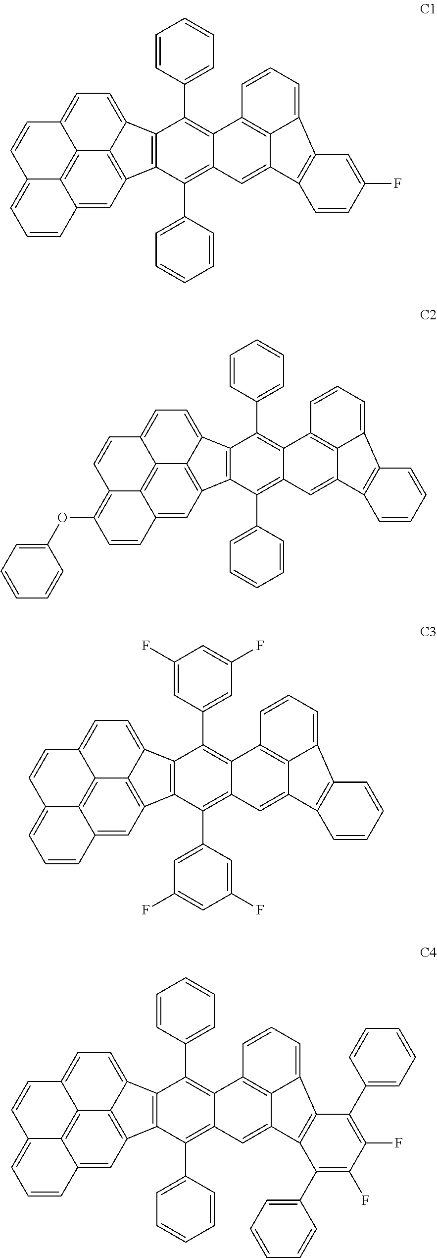
Exemplification of Organic Compound According to the Present Invention
Specific examples of the compounds represented by general formula (1) above are shown below. However, the present invention is not limited thereto.
Figure US08968889-20150303-C00006
Figure US08968889-20150303-C00007
Figure US08968889-20150303-C00008
Figure US08968889-20150303-C00009
Figure US08968889-20150303-C00010
Figure US08968889-20150303-C00011
Figure US08968889-20150303-C00012
Figure US08968889-20150303-C00013
Figure US08968889-20150303-C00014
Figure US08968889-20150303-C00015
Figure US08968889-20150303-C00016
Figure US08968889-20150303-C00017

Properties of Respective Exemplified Compound Groups
Among the exemplified compounds, the whole molecule of each compound shown in group A consists of only a hydrocarbon. Compounds consisting of only hydrocarbons have low HOMO energy levels. Accordingly, the oxidation potentials are low, which indicates that the organic compounds are stable against oxidation.
Accordingly, among the organic compounds according to the present invention, the compounds shown in group A consisting of only hydrocarbons are preferable because the stability of their molecules is high.
Some of the compounds of group A are compounds represented by general formula (2) below. Organic compounds according to the present invention are more preferably represented by general formula (2) below.
Figure US08968889-20150303-C00018
In general formula (2), R19 to R29 are each independently selected from an alkyl group and an aryl group.
This alkyl group is an alkyl group having 1 to 4 carbon atoms. Specifically, the alkyl group is a methyl group, an ethyl group, a n-propyl group, an isopropyl group, a n-butyl group, an isobutyl group, a sec-butyl group, or a tert-butyl group. A tert-butyl group is preferable because the tert-butyl group has an effect of suppressing molecular association by the steric hindrance.
This aryl group is a phenyl group, a naphthyl group, or a fluorenyl group. This is because these aryl groups are substituents suitable for shifting the emission wavelength to the long-wavelength side by about several nanometers to 20 nm in controlling the emission wavelength. The aryl group may further have a substituent. The substituent is an alkyl group having 1 to 4 carbon atoms or a phenyl group.
The two phenyl groups bonded to the basic structure in general formula (2) are substituents that suppress concentration quenching. When these phenyl groups have substituents, the effect of suppressing concentration quenching is further increased.
On the other hand, when a substituent contains a nitrogen atom as shown by the compounds in group B, the oxidation potential of the molecule significantly changes or the intermolecular interaction changes. When a substituent contains a nitrogen atom, the wavelength at which the intensity of a spectrum becomes maximum can be shifted to the long-wavelength side. Since the intermolecular interaction changes, in the case where a substituent contains a nitrogen atom, the compound can be used as an electron-transporting layer, a hole-transporting layer, or a light-emitting layer in a concentration of 100%.
Also, when a substituent contains a heteroatom other than a nitrogen atom as shown by the compounds in group C, the oxidation potential of the molecule also significantly changes or the intermolecular interaction changes. In some cases, a change more significantly than the case where a substituent contains a nitrogen atom can be expected. Since the intermolecular interaction changes, in the case where a substituent contains a heteroatom, the compound can be used as an electron-transporting layer, a hole-transporting layer, or a light-emitting layer in a concentration of 100%.
Exemplary compounds of group A to group C have been described. In these compounds, the basic structure itself can emit green light. In addition, when a substituent is introduced into the basic structure of the organic compound according to the present invention, the emission wavelength is shifted from green to the longer wavelength side. More specifically, such a substituted basic structure can emit red light. Furthermore, the application of the organic compound according to the present invention is not limited to a guest material of a light-emitting layer of an organic light-emitting device. Alternatively, the organic compound according to the present invention may be used as a host material of a light-emitting layer of an organic light-emitting device. Alternatively, the organic compound may be used in an electron-transporting layer, an electron injection layer, a hole-transporting layer, a hole injection layer, or a hole-blocking layer, or the like of an organic light-emitting device. In such a case, the luminescent color emitted by the organic light-emitting device is not limited. Furthermore, the organic compound according to the present invention can also be used as an assist material or a host material of a light-emitting layer of an organic light-emitting device that emits red light.
Description of Synthetic Route
An example of a synthetic route of the organic compound according to the present invention will be described. A reaction formula of the synthetic route is shown below. In the synthetic route shown by the reaction formula below, in the case where a substituent is introduced, the synthesis can be conducted while a hydrogen atom located at a position to be substituted is substituted with the target substituent. Examples of the substituent to be introduced include an alkyl group, a halogen atom, and a phenyl group.
Synthetic Route 1
Figure US08968889-20150303-C00019

Other Organic Compounds and Starting Materials
Various compounds can be synthesized by changing compounds D1 to D3 in the above reaction formula. Specific examples of the compounds are shown in Table 1 as synthesized compounds. Table 1 also shows compounds D1 to D3 which are starting materials used for obtaining the synthesized compounds.
TABLE 1
D1 D2 D3
Synthesis Example 1
Figure US08968889-20150303-C00020
Figure US08968889-20150303-C00021
Figure US08968889-20150303-C00022
Synthesis Example 2
Figure US08968889-20150303-C00023
Figure US08968889-20150303-C00024
Figure US08968889-20150303-C00025
Synthesis Example 3
Figure US08968889-20150303-C00026
Figure US08968889-20150303-C00027
Figure US08968889-20150303-C00028
Synthesis Example 4
Figure US08968889-20150303-C00029
Figure US08968889-20150303-C00030
Figure US08968889-20150303-C00031
Synthesis Example 5
Figure US08968889-20150303-C00032
Figure US08968889-20150303-C00033
Figure US08968889-20150303-C00034
Synthesis Example 6
Figure US08968889-20150303-C00035
Figure US08968889-20150303-C00036
Figure US08968889-20150303-C00037
Synthesis Example 7
Figure US08968889-20150303-C00038
Figure US08968889-20150303-C00039
Figure US08968889-20150303-C00040
Synthesis Example 8
Figure US08968889-20150303-C00041
Figure US08968889-20150303-C00042
Figure US08968889-20150303-C00043
Synthesis Example 9
Figure US08968889-20150303-C00044
Figure US08968889-20150303-C00045
Figure US08968889-20150303-C00046
Synthesized Exemplary
compound compound No.
Synthesis Example 1
Figure US08968889-20150303-C00047
A3 
Synthesis Example 2
Figure US08968889-20150303-C00048
A4 
Synthesis Example 3
Figure US08968889-20150303-C00049
A13
Synthesis Example 4
Figure US08968889-20150303-C00050
A14
Synthesis Example 5
Figure US08968889-20150303-C00051
A22
Synthesis Example 6
Figure US08968889-20150303-C00052
A31
Synthesis Example 7
Figure US08968889-20150303-C00053
A32
Synthesis Example 8
Figure US08968889-20150303-C00054
B1 
Synthesis Example 9
Figure US08968889-20150303-C00055
C3 

Organic Light-Emitting Device
An organic light-emitting device according to this embodiment will be described. The organic light-emitting device according to this embodiment includes a pair of electrodes, namely, an anode and a cathode, and an organic compound layer disposed between the anode and the cathode. This organic compound layer is a device including the organic compound according to the present invention.
The organic light-emitting device according to this embodiment may include a plurality of organic compound layers. Examples of these plurality of layers include a hole injection layer, a hole-transporting layer, a light-emitting layer, a hole-blocking layer, an exciton-blocking layer, an electron transporting layer, and an electron-injection layer. These layers can be appropriately used in combination.
When the organic compound according to this embodiment is used as a guest material in a light-emitting layer, the concentration of the guest material to a host material is preferably 0.1% by weight or more and 30% by weight or less, and more preferably 0.5% by weight or more and 10% by weight or less.
The inventors of the present invention have conducted various studies and found that a device in which the organic compound according to the present invention is used as a host material or a guest material, in particular, a guest material of a light-emitting layer had an optical output with a high quantum yield and a high luminance, and had high durability.
In the organic light-emitting device according to this embodiment, besides the organic compound according to the present invention, publicly known low-molecular weight and high-molecular weight hole injection materials, hole-transporting materials, host materials, guest materials, electron injection materials, electron-transporting materials, and the like can also be used in combination according to need.
Examples of the compounds will be described.
As materials used as a hole injection layer or a hole-transporting layer, materials having a high hole mobility are preferably used. Examples of the low-molecular weight and high-molecular weight materials having a hole injection performance or a hole transport performance include, but are not limited to, triarylamine derivatives, phenylenediamine derivatives, stilbene derivatives, phthalocyanine derivatives, porphyrin derivatives, poly(vinylcarbazole), poly(thiophene), and other electrically conductive polymers.
Table 2 shows specific structural formulae of the host materials. The host materials may be derivatives of the compounds represented by the structural formulae shown in Table 2. Examples of the host materials further include, but are not limited to, fused-ring compounds (such as fluorene derivatives, naphthalene derivatives, anthracene derivatives, pyrene derivatives, carbazole derivatives, quinoxaline derivatives, and quinoline derivatives), organoaluminum complexes such as tris(8-quinolinolato)aluminum, organozinc complexes, triphenylamine derivatives, and polymer derivatives such as poly(fluorene) derivatives and poly(phenylene) derivatives.
TABLE 2
Figure US08968889-20150303-C00056
H1
Figure US08968889-20150303-C00057
H2
Figure US08968889-20150303-C00058
H3
Figure US08968889-20150303-C00059
H4
Figure US08968889-20150303-C00060
H5
Figure US08968889-20150303-C00061
H6
Figure US08968889-20150303-C00062
H7
Figure US08968889-20150303-C00063
H8
Figure US08968889-20150303-C00064
H9
Figure US08968889-20150303-C00065
H10
Figure US08968889-20150303-C00066
H11
Figure US08968889-20150303-C00067
H12
Figure US08968889-20150303-C00068
H13
Figure US08968889-20150303-C00069
H14
Figure US08968889-20150303-C00070
H15
Figure US08968889-20150303-C00071
H16
Figure US08968889-20150303-C00072
H17
Figure US08968889-20150303-C00073
H18
Figure US08968889-20150303-C00074
H19
Figure US08968889-20150303-C00075
H20
Figure US08968889-20150303-C00076
H21
Figure US08968889-20150303-C00077
H22
Figure US08968889-20150303-C00078
H23
Figure US08968889-20150303-C00079
H24
Figure US08968889-20150303-C00080
H25
Figure US08968889-20150303-C00081
H26
Figure US08968889-20150303-C00082
H27
Figure US08968889-20150303-C00083
H28
The electron injection materials or the electron-transporting materials are selected in consideration of, for example, the balance with the hole mobility of the hole injection materials or the hole-transporting materials. Examples of the materials having an electron injection performance or an electron transport performance include, but are not limited to, oxadiazole derivatives, oxazole derivatives, pyrazine derivatives, triazole derivatives, triazine derivatives, quinoline derivatives, quinoxaline derivatives, phenanthroline derivatives, and organoaluminum complexes.
As anode materials, those having a work function as high as possible are preferable. Examples of the anode materials include metal elements such as gold, platinum, silver, copper, nickel, palladium, cobalt, selenium, vanadium, and tungsten; alloys thereof; and metal oxides such as tin oxide, zinc oxide, indium oxide, indium tin oxide (ITO), and indium zinc oxide. In addition, electrically conductive polymers such as polyaniline, polypyrrole, and polythiophene may also be used. These electrode materials may be used alone or in combinations of two or more materials. The anode may have a single-layer structure or a multi-layer structure.
On the other hand, as cathode materials, those having a low work function are preferable. Examples of the cathode materials include metal elements such as alkali metals, e.g., lithium; alkaline earth metals, e.g., calcium; aluminum; titanium; manganese; silver; lead; and chromium. Alloys combining these metal elements may also be used. For example, magnesium-silver, aluminum-lithium, or aluminum-magnesium can be used. Metal oxides such as indium tin oxide (ITO) may also be used. These electrode materials may be used as alone or in combinations of two or more materials. The cathode may have a single-layer structure or a multi-layer structure.
In the organic light-emitting device of this embodiment, a layer containing the organic compound according to the present invention and layers composed of the other organic compounds are formed by the methods described below. In general, each of the layers is formed by a vacuum evaporation method, an ionized evaporation method, a sputtering method, a method using plasma, or a known coating method (for example, spin coating, dipping, a cast method, a Langmuir Blodgett (LB) method, or an ink jet method) after a material is dissolved in a suitable solvent. Among these, when a layer is formed by, for example, the vacuum evaporation method or the solution coating method, crystallization does not tend to occur, and thus the resulting layer has good stability with time. When a layer is formed by the coating method, the material may be used in combination with a suitable binder resin.
Examples of the binder resin include, but are not limited to, polyvinylcarbazole resins, polycarbonate resins, polyester resins, acrylonitrile butadiene styrene (ABS) resins, acrylic resins, polyimide resins, phenolic resins, epoxy resins, silicone resins, and urea resins. These binder resins may be used alone as a homopolymer or a copolymer or used as a mixture of two or more types of resins. Furthermore, additives such as a known plasticizer, antioxidant, or ultraviolet absorber may be optionally used in combination.
Apparatus Including Organic Light-Emitting Device
An apparatus including an organic light-emitting device according to this embodiment will now be described.
The organic light-emitting device according to this embodiment can be used in a display apparatus or an illuminating device. In addition, the organic light-emitting device according to this embodiment can be used in an exposure light source of an electrophotographic image-forming apparatus or a backlight of a liquid crystal display apparatus.
The display apparatus includes a display unit including the organic light-emitting device according to this embodiment. This display unit includes a plurality of pixels. Each of the pixels includes the organic light-emitting device according to this embodiment and a thin-film transistor (TFT) device which is an example of a switching device. An anode or a cathode of this organic light-emitting device is connected to a drain electrode or a source electrode of the TFT device. The display apparatus can be used as an image display apparatus such as a personal computer (PC). The display apparatus may be an image input apparatus that further includes an image input unit.
The image input apparatus includes an image input unit to which information from an area CCD sensor, a linear CCD sensor, a memory card, or the like is input and a display unit configured to display the input information. Such an image input apparatus that further includes an imaging optical system constitutes an image pickup apparatus such as a digital camera. The display unit of such an image pickup apparatus or an ink jet printer may have both an image output function of displaying an image on the basis of image information input from the outside and an input function, as an operation panel, of inputting process information to the image. The display apparatus may be used as a display unit of a multifunction printer.
Next, a display apparatus including the organic light-emitting device according to this embodiment will be described. FIG. 1 is a schematic cross-sectional view of a display apparatus including organic light-emitting devices according to this embodiment and TFT devices which are an example of switching devices configured to switch emission/non-emission of the organic light-emitting devices. FIG. 1 shows two pairs of an organic light-emitting device and a TFT device. Although not shown in the figure, the display device may further include a transistor configured to control the light-emission luminance. The display apparatus performs a display by turning on or turning off the organic light-emitting devices by driving the switching devices in accordance with information, and transmit the information. The detailed structure of the display apparatus will be described below.
The display apparatus shown in FIG. 1 includes a substrate 1 composed of, for example, glass and a moisture-proof film 2 for protecting TFT devices or organic compound layers, the moisture-proof film 2 being disposed on the substrate 1. Reference numeral 3 indicates a metal gate electrode, reference numeral 4 indicates a gate insulating film, and reference numeral 5 indicates a semiconductor layer.
TFT devices 8 each include the semiconductor layer 5, a drain electrode 6, and a source electrode 7. An insulating film 9 is provided on the upper portion of the TFT devices 8. An anode 11 of an organic light-emitting device is connected to the source electrode 7 through a contact hole 10. However, the structure of the display apparatus is not limited to this. It is sufficient that either the anode or the cathode of the organic light-emitting device is connected to either the source electrode or the drain electrode of a TFT device.
In FIG. 1, a plurality of organic compound layers are shown as a single organic compound layer 12. A first protective layer 14 and a second protective layer 15 for suppressing degradation of the organic light-emitting devices are provided on a cathode 13.
EXAMPLES Example 1 Synthesis of Exemplary Compound A2
Figure US08968889-20150303-C00084
First, 10.5 g (48 mmol) of fluoranthene-3-amine (E1) was mixed with 300 mL of dimethylformamide at 0 degrees (Celsius). Next, 8.2 g (48 mmol) of N-bromosuccinimide was added to the mixture. The temperature was returned to room temperature, and the reaction mixture was stirred for eight hours. The reaction mixture was poured into water, and a precipitate was filtered. The precipitate was then recrystallized with ethanol. The resulting crystals were filtered, washed with heptane, and then dried. Thus, 29 g of a brown solid E2 was obtained (yield: 60%). Subsequently, 10 g (34 mmol) of E2 was put in a 500-mL round-bottom flask, and the inside of the reaction system was replaced with argon. Next, 150 mL of methoxycyclopentane was put in the flask in an argon atmosphere, and the solution was cooled to −75 degrees (Celsius). Next, 64 mL of a 1.6 M solution of n-butyllithium was added dropwise thereto. After the dropwise addition, the temperature of the reaction mixture was returned to room temperature, and stirring was conducted for one hour. Subsequently, the reaction mixture was again cooled to −75 degrees (Celsius), and 15 g of finely crushed dry ice was added to the mixture. The temperature of the reaction mixture was gradually returned to room temperature. After the temperature was returned to room temperature, stirring was conducted for eight hours, and 1 M hydrochloric acid was then added to the reaction mixture to terminate the reaction. Subsequently, extraction was conducted with ethyl acetate. The organic layer was concentrated to obtain a brown liquid. The liquid was purified by column chromatography (ethyl acetate/heptane=1:3), and recrystallized with chloroform/methanol. Thus, 2.5 g of E3 was obtained in the form of a brown powder (yield: 28%).
Figure US08968889-20150303-C00085
Next, 12.8 g (50 mmol) of E4 and 10.5 g (50 mmol) of E5 were put in 200 mL of ethanol, and the resulting mixture was heated to 60 degrees (Celsius). Subsequently, 20 mL of a 5 M aqueous potassium hydroxide solution was added dropwise thereto. After the dropwise addition, the reaction mixture was heated to 80 degrees (Celsius), stirring was conducted for two hours, and the reaction mixture was cooled. A precipitate was then filtered, and washed with water and ethanol. The precipitate was then dried by heating under reduced pressure at 80 degrees (Celsius). Thus, 18 g of a dark green solid E6 was obtained (yield: 85%).
Figure US08968889-20150303-C00086
Next, 2.1 g (5 mmol) of E6 and 1.57 g (6 mmol) of E3 were put in 50 mL of toluene, and the mixture was heated to 80 degrees (Celsius). Subsequently, 0.82 g (7 mmol) of isoamyl nitrite was then slowly added dropwise to the mixture. The reaction mixture was then stirred at 110 degrees (Celsius) for three hours. The reaction mixture was cooled, and washed with 100 mL of water twice. The resulting organic layer was washed with a saturated saline solution, and dried with magnesium sulfate. Subsequently, the resulting solution was filtered, and the filtrate was then concentrated to obtain a brown liquid. This liquid was purified by column chromatography (chloroform/heptane=1:3), and recrystallized with chloroform/methanol. Thus, 2.3 g of A2 was obtained in the form of yellow crystals (yield: 76%).
An emission spectrum of a toluene solution of Exemplary compound A2 with a concentration of 1×10⁵ mol/L was obtained by measuring photoluminescence at an excitation wavelength of 350 nm using a fluorescence spectrophotometer F-4500 produced by Hitachi, Ltd. According to the measurement result, the spectrum had a maximum intensity at 487 nm.
Example 2 Synthesis of Exemplary Compound A3
Exemplary compound A3 was obtained by the same reactions and purification procedures as those performed in Example 1 except that the organic compound E5 used in Example 1 was changed to an organic compound E7.
Figure US08968889-20150303-C00087
An emission spectrum of a toluene solution of Exemplary compound A3 with a concentration of 1×10⁻⁵ mol/L was obtained by measuring photoluminescence at an excitation wavelength of 350 nm using a fluorescence spectrophotometer F-4500 produced by Hitachi, Ltd. According to the measurement result, the spectrum had a maximum intensity at 488 nm.
Example 3 Synthesis of Exemplary Compound A4
Exemplary compound A4 was obtained by the same reactions and purification procedures as those performed in Example 1 except that the organic compound E5 used in Example 1 was changed to an organic compound E8.
Figure US08968889-20150303-C00088
An emission spectrum of a toluene solution of Exemplary compound A4 with a concentration of 1×10⁻⁵ mol/L was obtained by measuring photoluminescence at an excitation wavelength of 350 nm using a fluorescence spectrophotometer F-4500 produced by Hitachi, Ltd. According to the measurement result, the spectrum had a maximum intensity at 488 nm.
Example 4 Synthesis of Exemplary Compound A14
Exemplary compound A14 was obtained by the same reactions and purification procedures as those performed in Example 1 except that the organic compound E4 used in Example 1 was changed to an organic compound E9, and that the organic compound E5 used in Example 1 was changed to the organic compound E7.
Figure US08968889-20150303-C00089
An emission spectrum of a toluene solution of Exemplary compound A14 with a concentration of 1×10⁻⁵ mol/L was obtained by measuring photoluminescence at an excitation wavelength of 350 nm using a fluorescence spectrophotometer F-4500 produced by Hitachi, Ltd. According to the measurement result, the spectrum had a maximum intensity at 490 nm.
Examples 5 to 12 Fabrication of Organic Light-Emitting Devices
In each of Examples 5 to 12, an organic light-emitting device having a structure in which an anode, a hole-transporting layer, a light-emitting layer, a hole/exciton-blocking layer, an electron-transporting layer, and a cathode were sequentially stacked was fabricated. First, an ITO film having a thickness of 100 nm was patterned on a glass substrate. On the substrate having the ITO film thereon, the following organic layers and electrode layers were successively deposited by a resistance-heating vacuum evaporation method in a vacuum chamber at a pressure of 10−5 Pa so that the area of the facing electrodes was 3 mm2.
Hole-transporting layer (40 nm): G-1
Light-emitting layer (30 nm); Host: G-2, Guest: Exemplary compound (weight ratio 5%)
Hole/exciton-blocking layer (10 nm): G-3
Electron-transporting layer (30 nm): G-4
Metal electrode layer 1 (1 nm): LiF
Metal electrode layer 2 (100 nm): Al
Figure US08968889-20150303-C00090
As for characteristics of the organic light-emitting devices, current-voltage characteristics were measured with a micrometer 4140B manufactured by Hewlett-Packard Development Company, and the light-emission luminance was measured with a luminance meter BM7 manufactured by Topcon Corporation. The quantum yields and the voltages of Examples 5 to 12 are shown in Table 3.
TABLE 3
Quantum
yield Voltage
Guest G-2 (cd/A) (V)
Example 5 A2 H7 12 4.7
Example 6 A2 H10 14 4.7
Example 7 A3 H10 14 4.6
Example 8 A3 H28 15 4.8
Example 9 A13 H17 12 4.6
Example 10 A14 H4 16 4.8
Example 11 A22 H26 14 4.6
Example 12 A31 H13 12 4.7
Examples 13 to 16
In each of Examples 13 to 16, an organic light-emitting device having a structure in which an anode, a hole injection layer, a hole-transporting layer, a light-emitting layer, an electron-transporting layer, and an electron injection layer, and a cathode were sequentially stacked was fabricated.
The organic light-emitting device having a resonance structure was fabricated by the method described below. An aluminum alloy (AlNd) film having a thickness of 100 nm and functioning as a reflective anode was deposited on a glass substrate functioning as a support by a sputtering method. Furthermore, an ITO film having a thickness of 80 nm and functioning as a transparent anode was formed by a sputtering method. Next, an element isolation film composed of a polyimide resin and having a thickness of 1.5 micrometers was formed on the periphery of the anode, and an opening having a radius of 3 mm was formed. The substrate was sequentially subjected to ultrasonic washing with acetone and isopropyl alcohol (IPA). The substrate was then washed in boiling IPA, and dried. The surface of this substrate was further subjected to UV cleaning.
Furthermore, the following organic compounds were successively deposited by a resistance-heating vacuum evaporation method in a vacuum chamber at a pressure of 10−5 Pa. Subsequently, indium zinc oxide (IZO) was deposited as a cathode by a sputtering method, thus forming a transparent electrode having a thickness of 30 nm. After the formation of this electrode, sealing was performed in a nitrogen atmosphere. Thus, the organic light-emitting devices were fabricated.
Hole injection layer (135 nm): G-11
Hole-transporting layer (10 nm): G-12
Light-emitting layer (35 nm); Host: G-13, Guest: Exemplary compound (weight ratio 2%)
Electron-transporting layer (10 nm): G-14
Electron injection layer (70 nm): G-15 (weight ratio 80%), Li (weight ratio 20%)
Figure US08968889-20150303-C00091
As for characteristics of the organic light-emitting devices, current-voltage characteristics were measured with a microammeter 4140B manufactured by Hewlett-Packard Development Company, and the light-emission luminance was measured with a luminance meter BM7 manufactured by Topcon Corporation. The quantum yields and the voltages of Examples 13 to 16 are shown in Table 4.
TABLE 4
Quantum
yield Voltage
Guest G-13 (cd/A) (V)
Example 13 A3 H7 19 4.5
Example 14 A4 H28 18 4.5
Example 15 A14 H27 15 4.7
Example 16 A22 H24 17 4.7

Results and Discussion
The organic compound according to the present invention is a novel compound that has a high quantum yield and that realizes light emission suitable for green light. When the organic compound according to the present invention is used in an organic light-emitting device, a light-emitting device having good light-emission characteristics can be fabricated.
While the present invention has been described with reference to exemplary embodiments, it is to be understood that the invention is not limited to the disclosed exemplary embodiments. The scope of the following claims is to be accorded the broadest interpretation so as to encompass all such modifications and equivalent structures and functions.
This application claims the benefit of Japanese Patent Application No. 2010-078291, filed Mar. 30, 2010, which is hereby incorporated by reference herein in its entirety.
REFERENCE SIGNS LIST
    • 8 TFT device
    • 11 Anode
    • 12 Organic compound layer
    • 13 Cathode

Claims (11)

The invention claimed is:
1. An organic compound represented by general formula (1):
Figure US08968889-20150303-C00092
wherein R1 to R18 are each independently selected from a hydrogen atom, a halogen atom, a substituted or unsubstituted alkyl group, a substituted or unsubstituted alkoxy group, a substituted amino group, a substituted or unsubstituted aryl group, and a substituted or unsubstituted heterocyclic group.
2. The organic compound according to claim 1, wherein R1 to R18 are each independently selected from a hydrogen atom, a substituted or unsubstituted alkyl group having 1 to 4 carbon atoms, and a substituted or unsubstituted aryl group.
3. The organic compound according to claim 2, wherein the organic compound is represented by general formula (2):
Figure US08968889-20150303-C00093
wherein R19 to R29 are each independently selected from a hydrogen atom, a substituted or unsubstituted alkyl group having 1 to 4 carbon atoms, and a substituted or unsubstituted phenyl group.
4. An organic light-emitting device comprising:
a pair of electrodes; and
an organic compound layer disposed between the pair of electrodes,
wherein the organic compound layer contains the organic compound according to claim 1.
5. The organic light-emitting device according to claim 4, wherein the organic compound layer is a light-emitting layer.
6. The organic light-emitting device according to claim 5, wherein the organic light-emitting device emits green light.
7. A display device comprising:
a plurality of pixels,
wherein the plurality of pixels each include the organic light-emitting device according to claim 4 and a switching device connected to the organic light-emitting device.
8. An image input apparatus comprising:
a display unit configured to display an image; and
an image input unit configured to input the image,
wherein the display unit includes a plurality of pixels, and the plurality of pixels each include the organic light-emitting device according to claim 4 and a switching device connected to the organic light-emitting device.
9. An illuminating apparatus comprising the organic light-emitting device according to claim 4.
10. An electrophotographic image-forming apparatus comprising an exposure light source;
wherein the exposure light source comprises the organic light-emitting device according to claim 4.
11. An exposure light source of an electrophotographic image-forming apparatus comprising the organic light-emitting device according to claim 4.
US13/634,372 2010-03-30 2011-03-22 Organic compound and organic light-emitting device Active 2032-03-07 US8968889B2 (en)

Applications Claiming Priority (3)

Application Number Priority Date Filing Date Title
JP2010078291A JP4750893B1 (en) 2010-03-30 2010-03-30 Novel organic compounds and organic light emitting devices
JP2010-078291 2010-03-30
PCT/JP2011/001678 WO2011121935A1 (en) 2010-03-30 2011-03-22 Novel organic compound and organic light-emitting device

Publications (2)

Publication Number Publication Date
US20130002526A1 US20130002526A1 (en) 2013-01-03
US8968889B2 true US8968889B2 (en) 2015-03-03

Family

ID=44597083

Family Applications (1)

Application Number Title Priority Date Filing Date
US13/634,372 Active 2032-03-07 US8968889B2 (en) 2010-03-30 2011-03-22 Organic compound and organic light-emitting device

Country Status (3)

Country Link
US (1) US8968889B2 (en)
JP (1) JP4750893B1 (en)
WO (1) WO2011121935A1 (en)

Families Citing this family (6)

* Cited by examiner, † Cited by third party
Publication number Priority date Publication date Assignee Title
JP5713699B2 (en) 2011-01-20 2015-05-07 キヤノン株式会社 Organic compound, organic light emitting device and image display device
JP5777408B2 (en) 2011-05-30 2015-09-09 キヤノン株式会社 Fused polycyclic compound and organic light emitting device using the same
JP5946264B2 (en) * 2011-11-16 2016-07-06 ユー・ディー・シー アイルランド リミテッド ORGANIC ELECTROLUMINESCENT ELEMENT, ORGANIC ELECTROLUMINESCENT ELEMENT MATERIAL, LIGHT EMITTING DEVICE, DISPLAY DEVICE AND LIGHTING DEVICE USING THE ELEMENT
DE102013102233A1 (en) * 2013-03-06 2014-09-11 Emitec France S.A.S Process for withdrawing a liquid additive from a tank
JPWO2018066536A1 (en) 2016-10-03 2019-09-05 出光興産株式会社 COMPOUND, COMPOSITION, ORGANIC ELECTROLUMINESCENT DEVICE, AND ELECTRONIC DEVICE
JP6829583B2 (en) * 2016-11-09 2021-02-10 出光興産株式会社 Compounds, compositions, organic electroluminescence devices, and electronic devices

Citations (12)

* Cited by examiner, † Cited by third party
Publication number Priority date Publication date Assignee Title
JPH09241629A (en) 1996-03-08 1997-09-16 Idemitsu Kosan Co Ltd Organic electroluminescent element
JPH11255508A (en) 1998-03-09 1999-09-21 Mitsubishi Chemical Corp C70 derivative
WO2001023497A1 (en) 1999-09-30 2001-04-05 Idemitsu Kosan Co., Ltd. Organic electroluminescent element
US20020168544A1 (en) * 1999-12-28 2002-11-14 Idemitsu Kosan Co., Ltd. Organic electroluminescence device emitting white light
US20040076853A1 (en) * 2002-04-24 2004-04-22 Eastman Kodak Company Organic light-emitting diode devices with improved operational stability
JP2008290999A (en) 2007-05-28 2008-12-04 Canon Inc Indenochrysene derivative and organic light emitting device using the same
JP2009152529A (en) 2007-11-28 2009-07-09 Idemitsu Kosan Co Ltd Organic electroluminescent element using fluoranthene derivative
JP2009302470A (en) 2008-06-17 2009-12-24 Mitsui Chemicals Inc Organic transistor
WO2010013520A1 (en) 2008-07-30 2010-02-04 出光興産株式会社 Indenopyrene compound, organic thin film solar cell material using the same, and organic thin film solar cell
JP2010254610A (en) 2009-04-23 2010-11-11 Canon Inc New organic compound, light-emitting device and image display
JP2010270103A (en) 2009-04-23 2010-12-02 Canon Inc New organic compound, light-emitting device, and image display
JP2011037744A (en) 2009-08-10 2011-02-24 Canon Inc Organic compound and organic light-emitting device using the same

Patent Citations (12)

* Cited by examiner, † Cited by third party
Publication number Priority date Publication date Assignee Title
JPH09241629A (en) 1996-03-08 1997-09-16 Idemitsu Kosan Co Ltd Organic electroluminescent element
JPH11255508A (en) 1998-03-09 1999-09-21 Mitsubishi Chemical Corp C70 derivative
WO2001023497A1 (en) 1999-09-30 2001-04-05 Idemitsu Kosan Co., Ltd. Organic electroluminescent element
US20020168544A1 (en) * 1999-12-28 2002-11-14 Idemitsu Kosan Co., Ltd. Organic electroluminescence device emitting white light
US20040076853A1 (en) * 2002-04-24 2004-04-22 Eastman Kodak Company Organic light-emitting diode devices with improved operational stability
JP2008290999A (en) 2007-05-28 2008-12-04 Canon Inc Indenochrysene derivative and organic light emitting device using the same
JP2009152529A (en) 2007-11-28 2009-07-09 Idemitsu Kosan Co Ltd Organic electroluminescent element using fluoranthene derivative
JP2009302470A (en) 2008-06-17 2009-12-24 Mitsui Chemicals Inc Organic transistor
WO2010013520A1 (en) 2008-07-30 2010-02-04 出光興産株式会社 Indenopyrene compound, organic thin film solar cell material using the same, and organic thin film solar cell
JP2010254610A (en) 2009-04-23 2010-11-11 Canon Inc New organic compound, light-emitting device and image display
JP2010270103A (en) 2009-04-23 2010-12-02 Canon Inc New organic compound, light-emitting device, and image display
JP2011037744A (en) 2009-08-10 2011-02-24 Canon Inc Organic compound and organic light-emitting device using the same

Also Published As

Publication number Publication date
JP4750893B1 (en) 2011-08-17
US20130002526A1 (en) 2013-01-03
WO2011121935A1 (en) 2011-10-06
JP2011207829A (en) 2011-10-20

Similar Documents

Publication Publication Date Title
US9315460B2 (en) Organic compound, light-emitting device, and image display apparatus
US9019328B2 (en) Organic compound, organic light-emitting device, and display apparatus
US8293384B2 (en) Organic compound, light-emitting device, and image display apparatus
US8951648B2 (en) Diacenaphtho[1,2-b:1′,2′-k]chrysene derivative
KR101555111B1 (en) Organic compound, organic electroluminescence element, and image display device
US8963416B2 (en) Organic compound
US20170133598A1 (en) Novel organic compound, organic light emitting device, and image display device
US8968890B2 (en) Organic compound and organic light-emitting device having the same
US8968889B2 (en) Organic compound and organic light-emitting device
US9005778B2 (en) Organic compound and organic light-emitting device including the same
US9397298B2 (en) Organic compound, organic light-emitting device, and image display device
US9145344B2 (en) Organic compound and organic light-emitting device including the same
US9166173B2 (en) Organic compound
US20130299814A1 (en) Organic compound, organic light-emitting device, and image display apparatus
US9099656B2 (en) Organic compound and organic light-emitting device including same
US20110148292A1 (en) Organic compound and organic light-emitting device using the same

Legal Events

Date Code Title Description
AS Assignment

Owner name: CANON KABUSHIKI KAISHA, JAPAN

Free format text: ASSIGNMENT OF ASSIGNORS INTEREST;ASSIGNORS:KAMATANI, JUN;KISHINO, KENGO;YAMADA, NAOKI;AND OTHERS;REEL/FRAME:029369/0269

Effective date: 20120711

STCF Information on status: patent grant

Free format text: PATENTED CASE

MAFP Maintenance fee payment

Free format text: PAYMENT OF MAINTENANCE FEE, 4TH YEAR, LARGE ENTITY (ORIGINAL EVENT CODE: M1551); ENTITY STATUS OF PATENT OWNER: LARGE ENTITY

Year of fee payment: 4

MAFP Maintenance fee payment

Free format text: PAYMENT OF MAINTENANCE FEE, 8TH YEAR, LARGE ENTITY (ORIGINAL EVENT CODE: M1552); ENTITY STATUS OF PATENT OWNER: LARGE ENTITY

Year of fee payment: 8