US8964153B2 - In-plane switching mode liquid crystal display device and fabricating method thereof - Google Patents
In-plane switching mode liquid crystal display device and fabricating method thereof Download PDFInfo
- Publication number
- US8964153B2 US8964153B2 US11/168,371 US16837105A US8964153B2 US 8964153 B2 US8964153 B2 US 8964153B2 US 16837105 A US16837105 A US 16837105A US 8964153 B2 US8964153 B2 US 8964153B2
- Authority
- US
- United States
- Prior art keywords
- line
- data line
- light blocking
- substrate
- common electrode
- Prior art date
- Legal status (The legal status is an assumption and is not a legal conclusion. Google has not performed a legal analysis and makes no representation as to the accuracy of the status listed.)
- Active, expires
Links
Images


Classifications
-
- G—PHYSICS
- G02—OPTICS
- G02F—OPTICAL DEVICES OR ARRANGEMENTS FOR THE CONTROL OF LIGHT BY MODIFICATION OF THE OPTICAL PROPERTIES OF THE MEDIA OF THE ELEMENTS INVOLVED THEREIN; NON-LINEAR OPTICS; FREQUENCY-CHANGING OF LIGHT; OPTICAL LOGIC ELEMENTS; OPTICAL ANALOGUE/DIGITAL CONVERTERS
- G02F1/00—Devices or arrangements for the control of the intensity, colour, phase, polarisation or direction of light arriving from an independent light source, e.g. switching, gating or modulating; Non-linear optics
- G02F1/01—Devices or arrangements for the control of the intensity, colour, phase, polarisation or direction of light arriving from an independent light source, e.g. switching, gating or modulating; Non-linear optics for the control of the intensity, phase, polarisation or colour
- G02F1/13—Devices or arrangements for the control of the intensity, colour, phase, polarisation or direction of light arriving from an independent light source, e.g. switching, gating or modulating; Non-linear optics for the control of the intensity, phase, polarisation or colour based on liquid crystals, e.g. single liquid crystal display cells
- G02F1/133—Constructional arrangements; Operation of liquid crystal cells; Circuit arrangements
- G02F1/1333—Constructional arrangements; Manufacturing methods
- G02F1/1343—Electrodes
-
- G—PHYSICS
- G02—OPTICS
- G02F—OPTICAL DEVICES OR ARRANGEMENTS FOR THE CONTROL OF LIGHT BY MODIFICATION OF THE OPTICAL PROPERTIES OF THE MEDIA OF THE ELEMENTS INVOLVED THEREIN; NON-LINEAR OPTICS; FREQUENCY-CHANGING OF LIGHT; OPTICAL LOGIC ELEMENTS; OPTICAL ANALOGUE/DIGITAL CONVERTERS
- G02F1/00—Devices or arrangements for the control of the intensity, colour, phase, polarisation or direction of light arriving from an independent light source, e.g. switching, gating or modulating; Non-linear optics
- G02F1/01—Devices or arrangements for the control of the intensity, colour, phase, polarisation or direction of light arriving from an independent light source, e.g. switching, gating or modulating; Non-linear optics for the control of the intensity, phase, polarisation or colour
- G02F1/13—Devices or arrangements for the control of the intensity, colour, phase, polarisation or direction of light arriving from an independent light source, e.g. switching, gating or modulating; Non-linear optics for the control of the intensity, phase, polarisation or colour based on liquid crystals, e.g. single liquid crystal display cells
- G02F1/133—Constructional arrangements; Operation of liquid crystal cells; Circuit arrangements
- G02F1/136—Liquid crystal cells structurally associated with a semi-conducting layer or substrate, e.g. cells forming part of an integrated circuit
- G02F1/1362—Active matrix addressed cells
- G02F1/136209—Light shielding layers, e.g. black matrix, incorporated in the active matrix substrate, e.g. structurally associated with the switching element
-
- G—PHYSICS
- G02—OPTICS
- G02F—OPTICAL DEVICES OR ARRANGEMENTS FOR THE CONTROL OF LIGHT BY MODIFICATION OF THE OPTICAL PROPERTIES OF THE MEDIA OF THE ELEMENTS INVOLVED THEREIN; NON-LINEAR OPTICS; FREQUENCY-CHANGING OF LIGHT; OPTICAL LOGIC ELEMENTS; OPTICAL ANALOGUE/DIGITAL CONVERTERS
- G02F1/00—Devices or arrangements for the control of the intensity, colour, phase, polarisation or direction of light arriving from an independent light source, e.g. switching, gating or modulating; Non-linear optics
- G02F1/01—Devices or arrangements for the control of the intensity, colour, phase, polarisation or direction of light arriving from an independent light source, e.g. switching, gating or modulating; Non-linear optics for the control of the intensity, phase, polarisation or colour
- G02F1/13—Devices or arrangements for the control of the intensity, colour, phase, polarisation or direction of light arriving from an independent light source, e.g. switching, gating or modulating; Non-linear optics for the control of the intensity, phase, polarisation or colour based on liquid crystals, e.g. single liquid crystal display cells
- G02F1/133—Constructional arrangements; Operation of liquid crystal cells; Circuit arrangements
- G02F1/1333—Constructional arrangements; Manufacturing methods
- G02F1/1335—Structural association of cells with optical devices, e.g. polarisers or reflectors
- G02F1/133509—Filters, e.g. light shielding masks
- G02F1/133512—Light shielding layers, e.g. black matrix
-
- G—PHYSICS
- G02—OPTICS
- G02F—OPTICAL DEVICES OR ARRANGEMENTS FOR THE CONTROL OF LIGHT BY MODIFICATION OF THE OPTICAL PROPERTIES OF THE MEDIA OF THE ELEMENTS INVOLVED THEREIN; NON-LINEAR OPTICS; FREQUENCY-CHANGING OF LIGHT; OPTICAL LOGIC ELEMENTS; OPTICAL ANALOGUE/DIGITAL CONVERTERS
- G02F1/00—Devices or arrangements for the control of the intensity, colour, phase, polarisation or direction of light arriving from an independent light source, e.g. switching, gating or modulating; Non-linear optics
- G02F1/01—Devices or arrangements for the control of the intensity, colour, phase, polarisation or direction of light arriving from an independent light source, e.g. switching, gating or modulating; Non-linear optics for the control of the intensity, phase, polarisation or colour
- G02F1/13—Devices or arrangements for the control of the intensity, colour, phase, polarisation or direction of light arriving from an independent light source, e.g. switching, gating or modulating; Non-linear optics for the control of the intensity, phase, polarisation or colour based on liquid crystals, e.g. single liquid crystal display cells
- G02F1/133—Constructional arrangements; Operation of liquid crystal cells; Circuit arrangements
- G02F1/1333—Constructional arrangements; Manufacturing methods
- G02F1/1343—Electrodes
- G02F1/134309—Electrodes characterised by their geometrical arrangement
- G02F1/134363—Electrodes characterised by their geometrical arrangement for applying an electric field parallel to the substrate, i.e. in-plane switching [IPS]
Definitions
- the present invention relates to an in-plane switching mode liquid crystal display device, and more particularly, to an in-plane switching mode liquid crystal display device and a fabrication method thereof which can improve image quality by preventing VAC (Viewing Angle Cross Talk) deficiency.
- VAC Viewing Angle Cross Talk
- Liquid crystal displays are typically used as flat panel display devices which have low power consumption and provide high picture quality.
- a liquid crystal display device is formed by attaching face to face a thin film transistor array substrate and a color filter substrate with a uniform interval therebetween, and disposing a liquid crystal layer between the thin film transistor array substrate and the color filter substrate. Pixel regions are arranged on the thin film transistor array substrate in a matrix manner.
- a thin film transistor, a pixel electrode and a capacitor are formed within the pixel region.
- a common electrode and the pixel electrode -apply an electric field to the liquid crystal layer.
- An RGB color filter and a black matrix are formed on the color filter substrate.
- an alignment film is formed at surfaces of the thin film transistor array substrate and the color filter substrate facing each other and is rubbed to orient the liquid crystal material in a specified direction.
- the liquid crystal material rotates due to dielectric anisotropy.
- light is transmitted or blocked by pixels to display the image.
- a twisted nematic mode liquid crystal display device has a narrow viewing angle.
- an in-plane switching mode LCD has been recently introduced to improve the narrow viewing angle by aligning liquid crystal molecules in a substantially horizontal direction with respect to the substrate.
- FIGS. 1A and 1B schematically illustrates pixels of a typical in-plane switching mode liquid crystal display device.
- FIG. 1A is a plane view and FIG. 1B is a cross-sectional view taken along line I-I′ of FIG. 1A .
- gate lines 1 and data lines 3 are arranged horizontally and vertically on a first transparent substrate 10 to define the pixel regions.
- N gate lines 1 and M data lines 3 crossing each other to create N ⁇ M pixels, only two pixels are shown in the drawing for explanatory purposes.
- a thin film transistor 9 is disposed at a crossing of the gate line 1 and the data line 3 .
- the thin film transistor 9 includes a gate electrode 1 a , a semiconductor layer 5 and source/drain electrodes 2 a and 2 b .
- the gate electrode 1 a is connected to the gate line 1 .
- the source/drain electrodes 2 a and 2 b are connected to the data line 3 and a pixel electrode 7 , respectively.
- a gate insulation layer 8 is formed on the entire substrate 10 .
- a common line 4 is arranged parallel to the gate line 1 in the pixel region.
- a pair-of electrodes which are the common electrode 6 and the pixel electrode 7 , are arranged parallel to the data line 3 for switching liquid crystal molecules.
- the common electrode 6 is simultaneously formed with the gate line 1 and is connected to the common line 4 .
- the pixel electrode 7 is simultaneously formed with the source/drain electrodes 2 a and 2 b and is connected to the drain electrode 2 b .
- a passivation layer 11 is formed on the entire surface of the substrate 10 including the source/drain electrodes 2 a and 2 b .
- the pixel electrode line 14 formed to overlap the common line 4 forms a storage capacitor (Cst) with the gate insulation layer 8 interposed therebetween.
- a black matrix 21 and a color filter 23 are formed on a second substrate 20 , on which an overcoat layer (not shown) may be formed for flattening the color filter 23 .
- the black matrix 21 prevents light leakage where the thin film transistor 9 , the gate line 1 and the data line 3 are located.
- the color filter 23 provides color display capabilities to the liquid crystal display device.
- alignment films 12 a and 12 b are applied at the surfaces of the first and second substrates 10 and 20 facing each other. The alignment films 12 a and 12 b determine an initial alignment direction of the liquid crystal.
- a liquid crystal layer 13 is formed between the first and second substrates 10 and 20 .
- the liquid crystal layer 13 controls the light transmittance by a voltage applied between the common electrode 6 and the pixel electrode 7 .
- the conventional in-plane switching mode liquid crystal display device having such a construction can improve a viewing angle because the common electrode 6 and the pixel electrode 7 are arranged on the same substrate and generate an in-plane electric field.
- light leakage may occur at a specific viewing angle when misalignment between the common electrode 6 and the data line 3 of the first substrate 10 or misalignment between the first substrate 10 and the second substrate 20 occurs.
- FIGS. 2 and 3 are sectional views of a liquid crystal display device to illustrate the problems in the related art, wherein an alignment film is omitted.
- FIG. 2 when the misalignment between the common electrode 6 and the data line 3 occurs and therefore the data line 3 is shifted to the left, the data line 3 becomes relatively far from the common electrode 6 formed on a right pixel. Accordingly, light leakage (indicated by arrow in the drawing) through a gap between the data line 3 and the common electrode 6 of the right pixel occurs at a specific range of viewing angles. That is, when the viewer is in front of the LCD device, the light leakage can be blocked by the black matrix 21 formed on the second substrate 20 . However, when the viewer faces the LCD device within the specific range of viewing angles, the light leakage will be seen in that specific area where light is not blocked by the black matrix 21 .
- VAC Viewing Angle Cross Talk
- the black matrix 21 formed on the first substrate 10 inclines toward a left pixel. Therefore, light leakage occurs between the data line 3 and the common electrode 6 formed on the right side of the data line 3 .
- the VAC deficiency is observed only at the specific range of viewing angles.
- an object of the present invention is to provide an in-plane switching mode liquid crystal display device and a fabrication method thereof which can improve image quality and prevent VAC deficiency by forming a light blocking line for covering a gap between the data line and the common electrode adjacent to the data line.
- Another object of the present invention is to provide a liquid crystal display device and a fabrication method thereof which can improve an aperture ratio by forming at least one of a common electrode and a pixel electrode, which generate an in plane electric field in a pixel, of a transparent conductive material.
- an in-plane switching mode liquid crystal display device comprising: first and second substrates; a plurality of gate lines arranged in a first direction on the first substrate; a plurality of data lines arranged in a second direction crossing the first direction and defining pixels together with the gate lines; a switching device formed at a crossing of the gate line and the data line; at least one pair of a pixel electrode and a common electrode arranged toward the first direction and generating an in plane electric field in the pixel; a common line electrically connecting the common electrode; a light blocking line formed to cover space between the data line and the common electrode adjacent to the data line; and a liquid crystal layer formed between the first and second substrates.
- a liquid crystal display device comprising: first and second substrates; a plurality of gate lines arranged in a first direction on the first substrate; a plurality of common electrodes formed on the first substrate; a gate insulation layer formed over an entire surface of the first substrate including the gate lines and common electrodes; a plurality of data lines arranged in a second direction crossing the first direction on the gate insulation layer and defining pixel regions together with the gate lines; a passivation layer formed over the entire surface of the first substrate including the data lines; a plurality of pixel electrodes formed on the passivation layer and generating an in plane electric field in the pixel regions together with the common electrodes; a light blocking line formed to cover space between the data lines and the common electrodes adjacent to the data lines; and a liquid crystal layer formed between the first and second substrates.
- a liquid crystal display device comprising: first and second substrates; a plurality of gate lines arranged in a first direction on the first substrate; a plurality of common electrodes formed on the first substrate; a gate insulation layer formed over an entire surface of the first substrate including the gate lines and common electrodes; a plurality of data lines arranged in a second direction crossing the first direction on the gate insulation layer and defining pixel regions together with the gate lines; a plurality of pixel electrodes generating an in plane electric field in the pixel regions together with the common electrodes; a passivation layer formed over the entire surface of the first substrate including the data lines and the pixel electrodes; a light blocking line formed on the passivation layer and formed to cover space between the data lines and the common electrodes adjacent to the data lines; and a liquid crystal layer formed between the first and second substrates.
- a method for fabricating a liquid crystal display device providing first and second substrates; providing first and second substrates; forming a plurality of gate lines arranged in a first direction on the first substrate; forming a plurality of common electrodes formed on the first substrate; forming a gate insulation layer over an entire surface of the first substrate including the gate lines and common electrodes; forming a plurality of data lines arranged in a second direction crossing the first direction on the gate insulation layer and defining pixel regions together with the gate lines; forming a passivation layer over the entire surface of the first substrate including the data lines; forming a plurality of pixel electrodes on the passivation layer, for generating an in plane electric field in the pixel regions together with the common electrodes; forming a light blocking line on the passivation layer, for covering space between the data lines and the common electrodes adjacent to the data lines; and forming a liquid crystal layer
- FIGS. 1A and 1B illustrate a typical in-plane switching mode liquid crystal display device, wherein FIG. 1A is a plane view and FIG. 1B is a sectional view taken along line I-I′;
- FIG. 2 is a sectional view to describe problems of a liquid crystal display device in a related art
- FIG. 3 is a sectional view to describe problems of the liquid crystal display device in the related art
- FIGS. 4A and 4B illustrate a first embodiment of the present invention, wherein FIG. 4A is a plane view and FIG. 4B is a sectional view taken along line II-II′;
- FIGS. 5A and 5B illustrate a second embodiment of the present invention, wherein FIG. 5A is a plane view and FIG. 5B is a sectional view taken along line 111 -III′;
- FIGS. 6A and 6B illustrate a third embodiment of the present invention, wherein FIG. 5A is a plane view and FIG. 5B is a sectional view taken along line III-III′;
- FIGS. 7A to 7D illustrate fabrication processes of the in-plane switching mode liquid crystal display device in accordance with the second embodiment.
- FIGS. 8A to 8D illustrate fabrication processes of the in-plane switching mode liquid crystal display device in accordance with the second embodiment.
- FIGS. 4A and 4B illustrate an in-plane switching mode liquid crystal display device in accordance with a first embodiment of the present invention.
- FIG. 4A is a plane view illustrating two pixels in accordance with a first embodiment of the present invention
- FIG. 4B is a sectional view taken along line II-II′ of FIG. 4A .
- the gate lines 101 arranged in a first direction and the data lines 103 arranged in a second direction are formed on a first transparent substrate 110 to define pixel regions (P).
- a switching device 109 is formed at a crossing of the gate line 101 and the data line 103 .
- the switching device 109 is a thin film transistor, and includes a gate electrode 101 a formed by part of the gate line 101 , a semiconductor layer 105 formed on the gate electrode 101 a and source/drain electrodes 102 a and 102 b separated at a predetermined interval and arranged on the semiconductor layer 105 .
- At least a common electrode 106 and a pixel electrode 107 which generate an in-plane electric field are formed in the pixel region (P).
- the common electrode 106 and the pixel electrode 107 are arranged parallel to each other.
- the common electrodes 106 and 106 ′ and the pixel electrode 107 may have a bent structure.
- the data line 103 can have a bent structure together with the common electrode 106 and the pixel electrode 107 .
- the common electrode 106 and the pixel electrode 107 may be arranged parallel to the gate line 101 .
- the gate line 101 may have the bent structure.
- the common electrode 106 is electrically connected to a common line 104
- the pixel electrode 107 is electrically connected to a pixel electrode line 114 .
- the pixel electrode line 114 overlaps the common line 104 to form a storage capacitor (Cst).
- a light blocking line 150 is formed over the data line 103 .
- the light blocking line 150 covers a gap between the data line 103 and the common electrode 106 adjacent to the data line 103 , and overlaps part of the common electrode 106 .
- the light blocking line 150 may have the same bent structure as the data line 103 .
- the light blocking line 150 serves to prevent light leakage from the gap between the data line 103 and the common electrode 106 . That is, as described in the related art (Refer to FIGS. 2 and 3 ), because of the misalignment between the common electrode and the data line or the misalignment between the thin film transistor substrate and the color filter substrate, light leakage through the gap of the data line 103 and the common line 104 in the range of a specific viewing angle at the side of a liquid crystal panel generates the VAC deficiency.
- the light blocking line 150 solves the VAC deficiency by blocking light leaked in the range of the specific viewing angle when such misalignment occurs (misalignment between the common electrode and the data line or misalignment between the thin film transistor substrate and the color filter substrate).
- the light blocking line 150 may have the same bent structure as the data line 103 .
- the common electrode 106 is formed on the first substrate 110 , and a gate insulation layer 108 is formed on the first substrate 110 including the common electrode 106 .
- the pixel electrode 107 and the data line 103 are coplanar and are formed on the gate insulation layer 108 .
- a passivation layer 111 is formed on an entire surface of the gate insulation layer 108 including the pixel electrode 107 and the data line 103 .
- the light blocking line 150 is formed on the passivation layer 111 to cover the gap between the data line 103 and the common electrode 106 .
- the light blocking line 150 may be formed of a transparent conductive material such as ITO or IZO.
- the light blocking line 150 can be formed together when forming a gate pad and a data pad formed to supply a signal to the gate line 101 and the data line 103 .
- a black matrix 121 for preventing light leakage where the thin film transistor 109 , the gate line 101 and the data line 103 are located, and a color filter 123 providing color display capabilities are formed on a second substrate 120 .
- An overcoat film (not shown) is applied on the second substrate 120 in order to flatten the color filter 123 .
- alignment films 112 a and 112 b which determine an initial alignment direction of the liquid crystal are applied at the surfaces of the first and second substrates 110 and 120 facing each other.
- a liquid crystal layer 113 is formed between the first and second substrates 110 and 120 , and controls the light transmittance via a voltage applied between the common electrode 106 and the pixel electrode 107 .
- the color filter 123 may be formed on the first substrate 110 .
- the color filter 123 may be formed by a COT (color filter on TFT) structure where a color filter is formed on a thin film transistor or by a TOC (TFT on color filter) structure where a thin film transistor is formed on a color filter.
- COT color filter on TFT
- TOC TOC on color filter
- the first embodiment of the present invention having such a structure can prevent light leakage which occurs at a side viewing angle by the light blocking line 150 and therefore solve the VAC deficiency problem.
- the liquid crystal display device having such a structure reduces an aperture ratio since the common electrode 106 and the pixel electrode 107 arranged in the pixel region are formed of an opaque metal material. Accordingly, an embodiment of the present invention improves the aperture ratio by forming at least one of the common electrode and the pixel electrode of a transparent conductive material.
- FIGS. 5A and 5B and FIGS. 6A and 6B illustrate liquid crystal display devices in accordance with second and third embodiments of the present invention.
- FIGS. 5A and 5B illustrate the second embodiment of the present invention, wherein a pixel electrode is formed of a transparent material.
- FIGS. 6A and 6B illustrate the third embodiment of the present invention, wherein both a common electrode and a pixel electrode are formed of a transparent material.
- the second and third embodiments have the same components as the first embodiment, except for locations where the common electrode and the pixel electrode are formed and materials of which the common electrode and the pixel electrode are formed. Accordingly, only the differences from the first embodiment ( FIGS. 4A and 4B ) will be described in the second and third embodiments.
- FIG. 5A is a plane view of a liquid crystal display device in accordance with the second embodiment of the present invention.
- FIG. 5B is a sectional view taken along line III-III′ of FIG. 5A .
- a pixel electrode 207 is formed of a transparent conductive material such as ITO or IZO and a light blocking line 250 is formed together with the pixel electrode 207 . Accordingly, the pixel electrode 207 and the light blocking line 250 are formed on a passivation layer 211 , and the pixel electrode 207 is electrically connected to a drain electrode 202 b of a thin film transistor 209 through a drain contact hole 207 a .
- the common electrode 206 is formed on a first substrate 210 , and a data line 203 is formed on a gate insulation layer 208 formed on an entire surface of the first substrate 210 including the common electrode 206
- the pixel electrode 207 and the common electrode 206 may also have a bent structure, so as the data line 203 .
- a color filter 223 may be formed on the first substrate 210 .
- the color filter 223 may be formed by a COT (color filter on TFT) structure where a color filter is formed on a thin film transistor or by a TOC (TFT on color filter) structure where a thin film transistor is formed on a color filter.
- COT color filter on TFT
- TOC TOC on color filter
- an aperture ratio can be improved compared to the first embodiment.
- FIG. 6A is a plane view of a liquid crystal display device in accordance with the third embodiment of the present invention.
- FIG. 6B is a sectional view taken along line VI-VI′ of FIG. 6A .
- a common electrode 306 and a pixel electrode 307 generating an in-plane electric field in a pixel region are formed of a transparent conductive material such as ITO or IZO.
- a light blocking line 350 is integrally formed with the common electrode 306 adjacent to the data line 303 . That is, since the common electrode 306 and the light blocking line 350 are formed on the same plane (i.e., passivation layer 311 ), the light blocking line 350 is structurally connected to the common electrode 306 .
- a common line 304 electrically connected to the common electrode 306 is formed on a first substrate 310 .
- the common electrode 306 is connected to the common line 304 through a common electrode contact hole 306 a.
- a pixel electrode line 314 electrically connected to a pixel electrode 307 overlaps the common line 304 to form a storage capacitor (Cst).
- the common electrode 306 and the pixel electrode 307 may also have the bent structure.
- the color filter 323 may be formed on the first substrate 310 .
- the color filter 323 may be formed by a COT (color filter on TFT) structure where a color filter is formed on a thin film transistor or by a TOC (TFT on color filter) structure where a thin film transistor is formed on a color filter.
- COT color filter on TFT
- TOC TOC on color filter
- both the common electrode 306 and the pixel electrode 307 are formed of a transparent conductive material such as ITO or IZO.
- this embodiment can provide a strong electric field applied to a liquid crystal layer between two electrodes because the common electrode 306 and the pixel electrode 307 are formed on the same plane (i.e., passivation layer: 311 ).
- the strong electric field causes liquid crystal molecules in the liquid crystal layer to be switched at a higher speed, thereby facilitating the implementation of a moving picture.
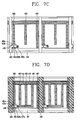
- FIGS. 7A to 7D and FIGS. 8A to 8D illustrate fabrication processes of the in-plane switching mode liquid crystal display device in accordance with the second embodiment.
- FIGS. 7A to 7D are plane views showing the fabrication processes
- FIGS. 8A to 8D are sectional views showing the fabrication processes.
- a transparent first substrate 410 is provided. Then, after a first metal material such as Cu, Ti, Cr, Al, Mo, Ta and an Al alloy is deposited over a first substrate 410 , the first metal material is patterned to form a gate line 401 , a gate electrode 401 a, a common line 404 arranged parallel to the gate line 401 , and a common electrode 406 perpendicularly diverged from the common line 404 .
- a first metal material such as Cu, Ti, Cr, Al, Mo, Ta and an Al alloy is deposited over a first substrate 410 .
- SiNx or SiOx is deposited over the entire surface of the substrate including the gate line 401 and the common electrode 406 by a plasma CVD method to thereby form a gate insulation layer 408 .
- amorphous silicon and n+ amorphous silicon are stacked on the gate insulation layer 408 .
- a second metal material such as Cu, Mo, Ta, Al, Cr, Ti, and Al alloy is deposited thereon.
- the amorphous silicon and n+ amorphous silicon and the second metal material are patterned to form a semiconductor layer 405 on the gate electrode 401 a , a data line 403 arranged perpendicular to the gate line 401 and defining pixel region together with the gate line 401 , and source and drain electrodes 402 a and 402 b separated at a predetermined interval on the semiconductor layer 405 .
- an inorganic material such as SiNx or SiOx or an organic material such as benzocyclobutene or acryl is applied on the substrate on which a thin film transistor 409 is formed, thereby forming a passivation layer 411 .
- a drain contact hole 407 a which exposes part of the drain electrode 402 b is formed.
- a transparent conductive material such as ITO (indium tin oxide) or IZO (indium zinc oxide) is deposited over the passivation layer 411 where the drain contact hole 407 a is formed. Thereafter, the transparent conductive material is patterned to form a pixel electrode 407 arranged parallel to the common electrode 406 for generating an in-plane electric field in the pixel together with the common electrode 406 , and to form a pixel electrode line 414 electrically connected to the pixel electrode 407 .
- the pixel electrode line 414 forms a storage capacitor (Cst) by overlapping the common line 404 .
- the light blocking line 450 for covering the gap between the data line 403 and the common electrode 406 adjacent to the data line 403 is formed on the passivation layer 411 . Also, the light blocking line 450 may be formed as a single line.
- the light preventing line 450 may be formed as two lines in order to cover the gap between the data line 403 and the common electrode 406 only but not to cover the portion directly above the data line 403 .
- a second substrate 420 where a black matrix 421 , a color filter 423 , and a second alignment film 412 b are formed is attached to the first substrate 410 , so that an in-plane liquid crystal display device can be formed.
- the present invention provides a light blocking line capable of blocking light leakage through the gap between the data line and the common electrode adjacent to the data line.
- the present invention does not limit the structures of the pixel electrode and the common electrode, materials which they are formed of, or the like.
- the present invention is to provide a light blocking line capable of blocking light leakage through the gap between the data line and the common electrode.
- the light blocking line can be formed as a single line or plural lines. Accordingly, the present invention may apply to all in-plane switching mode liquid crystal display devices provided with the light blocking line between the data line and the common electrode adjacent to the data line.
- the present invention in the in-plane switching mode liquid crystal display device, by providing the light blocking line between the data line and the common electrode adjacent to the data line, light leakage within a specific range of viewing angles can be prevented.
Landscapes
- Physics & Mathematics (AREA)
- Nonlinear Science (AREA)
- Mathematical Physics (AREA)
- Chemical & Material Sciences (AREA)
- Crystallography & Structural Chemistry (AREA)
- General Physics & Mathematics (AREA)
- Optics & Photonics (AREA)
- Engineering & Computer Science (AREA)
- Microelectronics & Electronic Packaging (AREA)
- Liquid Crystal (AREA)
Abstract
Description
Claims (12)
Applications Claiming Priority (2)
| Application Number | Priority Date | Filing Date | Title |
|---|---|---|---|
| KR10-2004-0050815 | 2004-06-30 | ||
| KR1020040050815A KR20060001662A (en) | 2004-06-30 | 2004-06-30 | Horizontal field type liquid crystal display device and manufacturing method thereof |
Publications (2)
| Publication Number | Publication Date |
|---|---|
| US20060001814A1 US20060001814A1 (en) | 2006-01-05 |
| US8964153B2 true US8964153B2 (en) | 2015-02-24 |
Family
ID=35513470
Family Applications (1)
| Application Number | Title | Priority Date | Filing Date |
|---|---|---|---|
| US11/168,371 Active 2027-08-10 US8964153B2 (en) | 2004-06-30 | 2005-06-29 | In-plane switching mode liquid crystal display device and fabricating method thereof |
Country Status (2)
| Country | Link |
|---|---|
| US (1) | US8964153B2 (en) |
| KR (1) | KR20060001662A (en) |
Cited By (2)
| Publication number | Priority date | Publication date | Assignee | Title |
|---|---|---|---|---|
| US20160190167A1 (en) * | 2009-02-18 | 2016-06-30 | Samsung Display Co., Ltd. | Thin-film transistor panel |
| US20160195789A1 (en) * | 2015-01-05 | 2016-07-07 | Samsung Display Co., Ltd. | Liquid crystal display |
Families Citing this family (19)
| Publication number | Priority date | Publication date | Assignee | Title |
|---|---|---|---|---|
| KR101229413B1 (en) | 2006-04-18 | 2013-02-04 | 엘지디스플레이 주식회사 | An array substrate for In-Plane switching mode LCD and method of fabricating of the same |
| KR20090110485A (en) * | 2008-04-18 | 2009-10-22 | 삼성전자주식회사 | Display substrate, liquid crystal display device and array substrate manufacturing method using same |
| KR101685046B1 (en) * | 2009-10-28 | 2016-12-12 | 삼성디스플레이 주식회사 | Display substrate, method for manufacturing the display substrate and display panel having the display substrate |
| CN102402086A (en) * | 2011-11-18 | 2012-04-04 | 深圳市华星光电技术有限公司 | Liquid crystal display device with a light guide plate |
| CN102967971B (en) * | 2012-11-02 | 2015-09-23 | 京东方科技集团股份有限公司 | Array base palte and display device |
| CN103278986B (en) * | 2013-04-01 | 2015-11-25 | 京东方科技集团股份有限公司 | The manufacture method of a kind of array base palte, display device and array base palte |
| US10180700B2 (en) * | 2013-07-01 | 2019-01-15 | Lg Display Co., Ltd. | Display device |
| US20160124274A1 (en) * | 2014-11-03 | 2016-05-05 | Shenzhen China Star Optoelectronics Technology Co. Ltd. | Display panel and display device |
| US10302844B2 (en) * | 2014-12-16 | 2019-05-28 | Apple Inc. | Display with backlight recycling structures |
| CN104950540B (en) * | 2015-07-20 | 2018-09-21 | 重庆京东方光电科技有限公司 | Array substrate and preparation method thereof and display device |
| CN105652548A (en) * | 2016-04-05 | 2016-06-08 | 深圳市华星光电技术有限公司 | Array substrate and liquid crystal display panel |
| CN106094372A (en) * | 2016-06-01 | 2016-11-09 | 深圳市华星光电技术有限公司 | Display panels, array base palte and preparation method thereof |
| CN106502011A (en) * | 2016-12-30 | 2017-03-15 | 深圳市华星光电技术有限公司 | Image element structure and method of work, array base palte |
| CN109557728B (en) * | 2017-09-25 | 2021-12-10 | 京东方科技集团股份有限公司 | Pixel structure, manufacturing method thereof, array substrate and touch display device |
| CN107632453B (en) * | 2017-10-31 | 2021-03-02 | 京东方科技集团股份有限公司 | Display panel, manufacturing method, and display device |
| US10642115B2 (en) * | 2018-03-30 | 2020-05-05 | Panasonic Liquid Crystal Display Co., Ltd. | Liquid crystal display device |
| CN113156651A (en) * | 2021-04-26 | 2021-07-23 | 京东方科技集团股份有限公司 | A display panel and display device |
| CN113885261A (en) * | 2021-09-30 | 2022-01-04 | Tcl华星光电技术有限公司 | Pixel unit of display panel, lower substrate of display panel and display panel |
| WO2025179520A1 (en) * | 2024-02-29 | 2025-09-04 | 京东方科技集团股份有限公司 | Liquid crystal display apparatus |
Citations (12)
| Publication number | Priority date | Publication date | Assignee | Title |
|---|---|---|---|---|
| US6133977A (en) * | 1997-10-21 | 2000-10-17 | Samsung Electronics Co., Ltd. | Liquid crystal displays having common electrode overlap with one or more data lines |
| US20010046019A1 (en) * | 1999-12-15 | 2001-11-29 | Lee Joun Ho | In-plane switching mode liquid crystal display |
| US20020044244A1 (en) * | 2000-08-30 | 2002-04-18 | Lee Joun Ho | In-plane switching mode liquid crystal display device and method for manufacturing the same |
| US20020057411A1 (en) * | 2000-11-14 | 2002-05-16 | Ik-Soo Kim | In-plane switching mode liquid crystal display device and manufacturing method thereof |
| US20020093614A1 (en) * | 2000-12-29 | 2002-07-18 | Hong-Man Moon | Substrate for in-plane switching mode liquid crystal display device and method for fabricating the same |
| US6577368B1 (en) * | 1997-11-03 | 2003-06-10 | Samsung Electronics Co., Ltd. | IPS-LCD having a third electrode having aperture and formed on counter substrate |
| US20040070717A1 (en) * | 2002-10-11 | 2004-04-15 | Lg.Philips Lcd Co., Ltd. | In-plane switching mode liquid crystal display device and fabrication method thereof |
| US20040212761A1 (en) * | 2003-04-25 | 2004-10-28 | Nec Lcd Technologies, Ltd | LCD device having a higher contrast ratio |
| US20050007524A1 (en) * | 2003-07-07 | 2005-01-13 | Au Optronics Corp. | Flat panel display with a non-matrix light shielding structure |
| US20050179846A1 (en) * | 2004-02-16 | 2005-08-18 | Lee Kyung H. | Fringe field switching liquid crystal display |
| US7027109B2 (en) * | 2001-08-03 | 2006-04-11 | Nec Corporation | TFT array substrate and active-matrix addressing liquid-crystal display device |
| US20070040978A1 (en) * | 2003-07-14 | 2007-02-22 | Yoshiaki Nakayoshi | Display device |
-
2004
- 2004-06-30 KR KR1020040050815A patent/KR20060001662A/en not_active Ceased
-
2005
- 2005-06-29 US US11/168,371 patent/US8964153B2/en active Active
Patent Citations (12)
| Publication number | Priority date | Publication date | Assignee | Title |
|---|---|---|---|---|
| US6133977A (en) * | 1997-10-21 | 2000-10-17 | Samsung Electronics Co., Ltd. | Liquid crystal displays having common electrode overlap with one or more data lines |
| US6577368B1 (en) * | 1997-11-03 | 2003-06-10 | Samsung Electronics Co., Ltd. | IPS-LCD having a third electrode having aperture and formed on counter substrate |
| US20010046019A1 (en) * | 1999-12-15 | 2001-11-29 | Lee Joun Ho | In-plane switching mode liquid crystal display |
| US20020044244A1 (en) * | 2000-08-30 | 2002-04-18 | Lee Joun Ho | In-plane switching mode liquid crystal display device and method for manufacturing the same |
| US20020057411A1 (en) * | 2000-11-14 | 2002-05-16 | Ik-Soo Kim | In-plane switching mode liquid crystal display device and manufacturing method thereof |
| US20020093614A1 (en) * | 2000-12-29 | 2002-07-18 | Hong-Man Moon | Substrate for in-plane switching mode liquid crystal display device and method for fabricating the same |
| US7027109B2 (en) * | 2001-08-03 | 2006-04-11 | Nec Corporation | TFT array substrate and active-matrix addressing liquid-crystal display device |
| US20040070717A1 (en) * | 2002-10-11 | 2004-04-15 | Lg.Philips Lcd Co., Ltd. | In-plane switching mode liquid crystal display device and fabrication method thereof |
| US20040212761A1 (en) * | 2003-04-25 | 2004-10-28 | Nec Lcd Technologies, Ltd | LCD device having a higher contrast ratio |
| US20050007524A1 (en) * | 2003-07-07 | 2005-01-13 | Au Optronics Corp. | Flat panel display with a non-matrix light shielding structure |
| US20070040978A1 (en) * | 2003-07-14 | 2007-02-22 | Yoshiaki Nakayoshi | Display device |
| US20050179846A1 (en) * | 2004-02-16 | 2005-08-18 | Lee Kyung H. | Fringe field switching liquid crystal display |
Cited By (3)
| Publication number | Priority date | Publication date | Assignee | Title |
|---|---|---|---|---|
| US20160190167A1 (en) * | 2009-02-18 | 2016-06-30 | Samsung Display Co., Ltd. | Thin-film transistor panel |
| US10825840B2 (en) * | 2009-02-18 | 2020-11-03 | Samsung Display Co., Ltd. | Thin-film transistor panel |
| US20160195789A1 (en) * | 2015-01-05 | 2016-07-07 | Samsung Display Co., Ltd. | Liquid crystal display |
Also Published As
| Publication number | Publication date |
|---|---|
| US20060001814A1 (en) | 2006-01-05 |
| KR20060001662A (en) | 2006-01-06 |
Similar Documents
| Publication | Publication Date | Title |
|---|---|---|
| US8964153B2 (en) | In-plane switching mode liquid crystal display device and fabricating method thereof | |
| US8040481B2 (en) | In-plane switching mode liquid crystal display device having first and second common electrode connection lines and first and second pixel electrode connection linesbeing formed on the same layer | |
| US7349051B2 (en) | In plane switching mode liquid crystal display device having particular common lines | |
| US7388639B2 (en) | In-plane switching mode liquid crystal display device having multi-domains | |
| US7916258B2 (en) | In-plane switching LCD panel | |
| US7671954B2 (en) | Liquid crystal display device and method for fabricating the same | |
| KR101818452B1 (en) | Liquid crystal display device and method for fabricating the same | |
| US9500923B2 (en) | Liquid crystal display device and method of fabricating the same | |
| JP2010014847A (en) | Liquid crystal display panel | |
| US7006186B2 (en) | In-plane switching mode liquid crystal display device and method of fabricating the same | |
| US7385661B2 (en) | In-plane switching mode liquid crystal display device and method of manufacturing the same | |
| US7663723B2 (en) | In-plane switching mode liquid crystal display device and fabrication method thereof | |
| US7388640B2 (en) | In-plane switching mode liquid crystal device with the common electrode auxiliary line not generating an electric field for driving liquid crystal in the sub-pixel regions | |
| US7649604B2 (en) | In-plane switching mode liquid crystal display device and method of fabricating thereof | |
| JP5197193B2 (en) | LCD panel | |
| KR101960363B1 (en) | Liquid crystal display device and method of fabricating the same | |
| US7532293B2 (en) | In plane switching LCD with alternating common and pixel electrodes having polygonal lattice shapes | |
| CN101097366A (en) | Thin film transistor substrates for liquid crystal displays | |
| KR100585872B1 (en) | Horizontal field type liquid crystal display device and manufacturing method thereof | |
| KR101318247B1 (en) | Liquid crystal display device and method for manufacturing of the same | |
| KR20070008882A (en) | LCD and its manufacturing method | |
| KR100918651B1 (en) | Transverse electric field type liquid crystal display device and its manufacturing method | |
| KR20050063006A (en) | In plane switching mode liquid crystal display device and method for fabricating thereof | |
| KR20070092896A (en) | LCD display device | |
| JP2010181837A (en) | Liquid crystal display device |
Legal Events
| Date | Code | Title | Description |
|---|---|---|---|
| AS | Assignment |
Owner name: LG.PHILIPS LCD CO., LTD., KOREA, REPUBLIC OF Free format text: ASSIGNMENT OF ASSIGNORS INTEREST;ASSIGNORS:PAIK, SANG YOON;NAM, SUNG-LIM;REEL/FRAME:016742/0695 Effective date: 20050624 |
|
| AS | Assignment |
Owner name: LG DISPLAY CO., LTD., KOREA, REPUBLIC OF Free format text: CHANGE OF NAME;ASSIGNOR:LG.PHILIPS LCD CO., LTD.;REEL/FRAME:020985/0675 Effective date: 20080304 Owner name: LG DISPLAY CO., LTD.,KOREA, REPUBLIC OF Free format text: CHANGE OF NAME;ASSIGNOR:LG.PHILIPS LCD CO., LTD.;REEL/FRAME:020985/0675 Effective date: 20080304 |
|
| FEPP | Fee payment procedure |
Free format text: PAYOR NUMBER ASSIGNED (ORIGINAL EVENT CODE: ASPN); ENTITY STATUS OF PATENT OWNER: LARGE ENTITY |
|
| STCF | Information on status: patent grant |
Free format text: PATENTED CASE |
|
| MAFP | Maintenance fee payment |
Free format text: PAYMENT OF MAINTENANCE FEE, 4TH YEAR, LARGE ENTITY (ORIGINAL EVENT CODE: M1551) Year of fee payment: 4 |
|
| MAFP | Maintenance fee payment |
Free format text: PAYMENT OF MAINTENANCE FEE, 8TH YEAR, LARGE ENTITY (ORIGINAL EVENT CODE: M1552); ENTITY STATUS OF PATENT OWNER: LARGE ENTITY Year of fee payment: 8 |