US8937023B2 - Method of manufacturing porous insulating film - Google Patents
Method of manufacturing porous insulating film Download PDFInfo
- Publication number
- US8937023B2 US8937023B2 US13/363,638 US201213363638A US8937023B2 US 8937023 B2 US8937023 B2 US 8937023B2 US 201213363638 A US201213363638 A US 201213363638A US 8937023 B2 US8937023 B2 US 8937023B2
- Authority
- US
- United States
- Prior art keywords
- insulating film
- porous insulating
- hydrocarbon group
- manufacturing
- hydrocarbon
- Prior art date
- Legal status (The legal status is an assumption and is not a legal conclusion. Google has not performed a legal analysis and makes no representation as to the accuracy of the status listed.)
- Active, expires
Links
- 238000004519 manufacturing process Methods 0.000 title claims description 28
- 125000001183 hydrocarbyl group Chemical group 0.000 claims abstract description 72
- -1 cyclic siloxane compound Chemical class 0.000 claims abstract description 65
- 239000000758 substrate Substances 0.000 claims abstract description 25
- 239000002210 silicon-based material Substances 0.000 claims abstract description 24
- 239000011148 porous material Substances 0.000 claims description 31
- 229930195733 hydrocarbon Natural products 0.000 claims description 27
- 239000004215 Carbon black (E152) Substances 0.000 claims description 21
- 239000001257 hydrogen Substances 0.000 claims description 15
- 229910052739 hydrogen Inorganic materials 0.000 claims description 15
- 125000004435 hydrogen atom Chemical class [H]* 0.000 claims description 15
- 125000004432 carbon atom Chemical group C* 0.000 claims description 14
- 239000007789 gas Substances 0.000 claims description 14
- 125000004122 cyclic group Chemical group 0.000 claims description 13
- 229910052710 silicon Inorganic materials 0.000 claims description 13
- 125000002619 bicyclic group Chemical group 0.000 claims description 12
- 150000002430 hydrocarbons Chemical class 0.000 claims description 12
- XUIMIQQOPSSXEZ-UHFFFAOYSA-N Silicon Chemical compound [Si] XUIMIQQOPSSXEZ-UHFFFAOYSA-N 0.000 claims description 10
- 239000010703 silicon Substances 0.000 claims description 10
- 239000004065 semiconductor Substances 0.000 claims description 9
- 125000000753 cycloalkyl group Chemical group 0.000 claims description 8
- 239000000178 monomer Substances 0.000 claims description 6
- 229910052760 oxygen Inorganic materials 0.000 claims description 6
- 239000002245 particle Substances 0.000 claims description 4
- 125000004429 atom Chemical group 0.000 claims description 3
- QVGXLLKOCUKJST-UHFFFAOYSA-N atomic oxygen Chemical compound [O] QVGXLLKOCUKJST-UHFFFAOYSA-N 0.000 claims description 3
- 239000001301 oxygen Substances 0.000 claims description 3
- 229920006395 saturated elastomer Polymers 0.000 claims description 2
- 239000007800 oxidant agent Substances 0.000 claims 2
- 238000000034 method Methods 0.000 abstract description 25
- 0 [1*][Si]1(C=C)O[Si]([2*])(C=C)O[Si]([3*])(C=C)O1 Chemical compound [1*][Si]1(C=C)O[Si]([2*])(C=C)O[Si]([3*])(C=C)O1 0.000 description 15
- 239000010410 layer Substances 0.000 description 12
- 239000003361 porogen Substances 0.000 description 12
- 230000008569 process Effects 0.000 description 9
- 150000001336 alkenes Chemical class 0.000 description 7
- 150000001345 alkine derivatives Chemical class 0.000 description 7
- 150000004703 alkoxides Chemical group 0.000 description 7
- 125000000217 alkyl group Chemical group 0.000 description 7
- 125000003277 amino group Chemical group 0.000 description 7
- ISWSIDIOOBJBQZ-UHFFFAOYSA-N phenol group Chemical group C1(=CC=CC=C1)O ISWSIDIOOBJBQZ-UHFFFAOYSA-N 0.000 description 7
- 125000001997 phenyl group Chemical group [H]C1=C([H])C([H])=C(*)C([H])=C1[H] 0.000 description 7
- XLYOFNOQVPJJNP-UHFFFAOYSA-N water Substances O XLYOFNOQVPJJNP-UHFFFAOYSA-N 0.000 description 7
- 230000001678 irradiating effect Effects 0.000 description 6
- 238000010521 absorption reaction Methods 0.000 description 5
- 229910052756 noble gas Inorganic materials 0.000 description 5
- 230000002776 aggregation Effects 0.000 description 4
- 238000004220 aggregation Methods 0.000 description 4
- 238000009792 diffusion process Methods 0.000 description 4
- KPUWHANPEXNPJT-UHFFFAOYSA-N disiloxane Chemical class [SiH3]O[SiH3] KPUWHANPEXNPJT-UHFFFAOYSA-N 0.000 description 4
- VYPSYNLAJGMNEJ-UHFFFAOYSA-N Silicium dioxide Chemical compound O=[Si]=O VYPSYNLAJGMNEJ-UHFFFAOYSA-N 0.000 description 3
- 230000000052 comparative effect Effects 0.000 description 3
- 239000010949 copper Substances 0.000 description 3
- 230000003247 decreasing effect Effects 0.000 description 3
- 238000010586 diagram Methods 0.000 description 3
- 239000011229 interlayer Substances 0.000 description 3
- 230000001590 oxidative effect Effects 0.000 description 3
- 230000005855 radiation Effects 0.000 description 3
- 239000000126 substance Substances 0.000 description 3
- XKRFYHLGVUSROY-UHFFFAOYSA-N Argon Chemical compound [Ar] XKRFYHLGVUSROY-UHFFFAOYSA-N 0.000 description 2
- RTZKZFJDLAIYFH-UHFFFAOYSA-N Diethyl ether Chemical compound CCOCC RTZKZFJDLAIYFH-UHFFFAOYSA-N 0.000 description 2
- LFQSCWFLJHTTHZ-UHFFFAOYSA-N Ethanol Chemical compound CCO LFQSCWFLJHTTHZ-UHFFFAOYSA-N 0.000 description 2
- 238000004380 ashing Methods 0.000 description 2
- 230000004888 barrier function Effects 0.000 description 2
- 150000001875 compounds Chemical class 0.000 description 2
- 230000008021 deposition Effects 0.000 description 2
- NBBQQQJUOYRZCA-UHFFFAOYSA-N diethoxymethylsilane Chemical compound CCOC([SiH3])OCC NBBQQQJUOYRZCA-UHFFFAOYSA-N 0.000 description 2
- JJQZDUKDJDQPMQ-UHFFFAOYSA-N dimethoxy(dimethyl)silane Chemical compound CO[Si](C)(C)OC JJQZDUKDJDQPMQ-UHFFFAOYSA-N 0.000 description 2
- 230000000694 effects Effects 0.000 description 2
- 238000005530 etching Methods 0.000 description 2
- 238000007654 immersion Methods 0.000 description 2
- 239000011261 inert gas Substances 0.000 description 2
- 239000002184 metal Substances 0.000 description 2
- 229910052751 metal Inorganic materials 0.000 description 2
- 239000002243 precursor Substances 0.000 description 2
- 229910052814 silicon oxide Inorganic materials 0.000 description 2
- 125000000391 vinyl group Chemical group [H]C([*])=C([H])[H] 0.000 description 2
- NAWXUBYGYWOOIX-SFHVURJKSA-N (2s)-2-[[4-[2-(2,4-diaminoquinazolin-6-yl)ethyl]benzoyl]amino]-4-methylidenepentanedioic acid Chemical compound C1=CC2=NC(N)=NC(N)=C2C=C1CCC1=CC=C(C(=O)N[C@@H](CC(=C)C(O)=O)C(O)=O)C=C1 NAWXUBYGYWOOIX-SFHVURJKSA-N 0.000 description 1
- GEONDYJEJWKSPD-UHFFFAOYSA-N 2,2,4,4,6,6,8-heptakis(ethenyl)-1,3,5,7,2,4,6,8-tetraoxatetrasilocane Chemical class C=C[SiH]1O[Si](O[Si](O[Si](O1)(C=C)C=C)(C=C)C=C)(C=C)C=C GEONDYJEJWKSPD-UHFFFAOYSA-N 0.000 description 1
- FEAWVQWPQVPUNT-UHFFFAOYSA-N 2,2,4,4,6,6-hexakis(ethenyl)-1,3,5,7,2,4,6,8-tetraoxatetrasilocane Chemical class C=C[Si]1(O[SiH2]O[Si](O[Si](O1)(C=C)C=C)(C=C)C=C)C=C FEAWVQWPQVPUNT-UHFFFAOYSA-N 0.000 description 1
- YNYXTKWMSKVUIM-UHFFFAOYSA-N 2,2,4,4,6-pentakis(ethenyl)-1,3,5,7,2,4,6,8-tetraoxatetrasilocane Chemical class C=C[SiH]1O[SiH2]O[Si](O[Si](O1)(C=C)C=C)(C=C)C=C YNYXTKWMSKVUIM-UHFFFAOYSA-N 0.000 description 1
- NCJZKGDZBMVUAX-UHFFFAOYSA-N 2,2-bis(ethenyl)-1,3,5,2,4,6-trioxatrisilinane Chemical class C=C[Si]1(O[SiH2]O[SiH2]O1)C=C NCJZKGDZBMVUAX-UHFFFAOYSA-N 0.000 description 1
- PXVVULBJLNNCDB-UHFFFAOYSA-N 2,2-bis(ethenyl)-1,3,5,7,2,4,6,8-tetraoxatetrasilocane Chemical class C=C[Si]1(O[SiH2]O[SiH2]O[SiH2]O1)C=C PXVVULBJLNNCDB-UHFFFAOYSA-N 0.000 description 1
- SXYYZYIAINPSAK-UHFFFAOYSA-N 2-(furan-2-yloxy)furan Chemical compound C=1C=COC=1OC1=CC=CO1 SXYYZYIAINPSAK-UHFFFAOYSA-N 0.000 description 1
- OWMXUQBMZMDCJB-UHFFFAOYSA-N 2-ethenyl-1,3,5,2,4,6-trioxatrisilinane Chemical class C=C[SiH]1O[SiH2]O[SiH2]O1 OWMXUQBMZMDCJB-UHFFFAOYSA-N 0.000 description 1
- JGWUKKFNKOUBPW-UHFFFAOYSA-N 2-ethenyl-1,3,5,7,2,4,6,8-tetraoxatetrasilocane Chemical class C=C[SiH]1O[SiH2]O[SiH2]O[SiH2]O1 JGWUKKFNKOUBPW-UHFFFAOYSA-N 0.000 description 1
- QQBUHYQVKJQAOB-UHFFFAOYSA-N 2-ethenylfuran Chemical compound C=CC1=CC=CO1 QQBUHYQVKJQAOB-UHFFFAOYSA-N 0.000 description 1
- CGRZDAWPHKFQSQ-YTEMWHBBSA-N C[SiH](C)(C)(/C=C/C1=CC2=C(C=C1)CC2)O[SiH](C)(C)(C)/C=C/C1=CC2=C(C=C1)CC2 Chemical compound C[SiH](C)(C)(/C=C/C1=CC2=C(C=C1)CC2)O[SiH](C)(C)(C)/C=C/C1=CC2=C(C=C1)CC2 CGRZDAWPHKFQSQ-YTEMWHBBSA-N 0.000 description 1
- OKTJSMMVPCPJKN-UHFFFAOYSA-N Carbon Chemical compound [C] OKTJSMMVPCPJKN-UHFFFAOYSA-N 0.000 description 1
- RYGMFSIKBFXOCR-UHFFFAOYSA-N Copper Chemical compound [Cu] RYGMFSIKBFXOCR-UHFFFAOYSA-N 0.000 description 1
- MYMOFIZGZYHOMD-UHFFFAOYSA-N Dioxygen Chemical compound O=O MYMOFIZGZYHOMD-UHFFFAOYSA-N 0.000 description 1
- 229910018557 Si O Inorganic materials 0.000 description 1
- 229910020175 SiOH Inorganic materials 0.000 description 1
- 230000009471 action Effects 0.000 description 1
- 229910052786 argon Inorganic materials 0.000 description 1
- 230000015572 biosynthetic process Effects 0.000 description 1
- 229910052799 carbon Inorganic materials 0.000 description 1
- 238000006243 chemical reaction Methods 0.000 description 1
- 239000000470 constituent Substances 0.000 description 1
- 229910052802 copper Inorganic materials 0.000 description 1
- 230000007850 degeneration Effects 0.000 description 1
- 230000003292 diminished effect Effects 0.000 description 1
- 229910001882 dioxygen Inorganic materials 0.000 description 1
- 230000009977 dual effect Effects 0.000 description 1
- 150000002170 ethers Chemical class 0.000 description 1
- 125000002541 furyl group Chemical group 0.000 description 1
- 238000010438 heat treatment Methods 0.000 description 1
- 239000001307 helium Substances 0.000 description 1
- 229910052734 helium Inorganic materials 0.000 description 1
- SWQJXJOGLNCZEY-UHFFFAOYSA-N helium atom Chemical compound [He] SWQJXJOGLNCZEY-UHFFFAOYSA-N 0.000 description 1
- 239000011810 insulating material Substances 0.000 description 1
- 150000002739 metals Chemical class 0.000 description 1
- 238000009832 plasma treatment Methods 0.000 description 1
- 239000002994 raw material Substances 0.000 description 1
- 230000009467 reduction Effects 0.000 description 1
- 239000000377 silicon dioxide Substances 0.000 description 1
- LIVNPJMFVYWSIS-UHFFFAOYSA-N silicon monoxide Inorganic materials [Si-]#[O+] LIVNPJMFVYWSIS-UHFFFAOYSA-N 0.000 description 1
- 238000001988 small-angle X-ray diffraction Methods 0.000 description 1
- 238000000235 small-angle X-ray scattering Methods 0.000 description 1
- 239000004094 surface-active agent Substances 0.000 description 1
- 238000009423 ventilation Methods 0.000 description 1
- 229920002554 vinyl polymer Polymers 0.000 description 1
- 229910052724 xenon Inorganic materials 0.000 description 1
- FHNFHKCVQCLJFQ-UHFFFAOYSA-N xenon atom Chemical compound [Xe] FHNFHKCVQCLJFQ-UHFFFAOYSA-N 0.000 description 1
Images


Classifications
-
- C—CHEMISTRY; METALLURGY
- C23—COATING METALLIC MATERIAL; COATING MATERIAL WITH METALLIC MATERIAL; CHEMICAL SURFACE TREATMENT; DIFFUSION TREATMENT OF METALLIC MATERIAL; COATING BY VACUUM EVAPORATION, BY SPUTTERING, BY ION IMPLANTATION OR BY CHEMICAL VAPOUR DEPOSITION, IN GENERAL; INHIBITING CORROSION OF METALLIC MATERIAL OR INCRUSTATION IN GENERAL
- C23C—COATING METALLIC MATERIAL; COATING MATERIAL WITH METALLIC MATERIAL; SURFACE TREATMENT OF METALLIC MATERIAL BY DIFFUSION INTO THE SURFACE, BY CHEMICAL CONVERSION OR SUBSTITUTION; COATING BY VACUUM EVAPORATION, BY SPUTTERING, BY ION IMPLANTATION OR BY CHEMICAL VAPOUR DEPOSITION, IN GENERAL
- C23C16/00—Chemical coating by decomposition of gaseous compounds, without leaving reaction products of surface material in the coating, i.e. chemical vapour deposition [CVD] processes
- C23C16/22—Chemical coating by decomposition of gaseous compounds, without leaving reaction products of surface material in the coating, i.e. chemical vapour deposition [CVD] processes characterised by the deposition of inorganic material, other than metallic material
- C23C16/30—Deposition of compounds, mixtures or solid solutions, e.g. borides, carbides, nitrides
- C23C16/40—Oxides
- C23C16/401—Oxides containing silicon
-
- C—CHEMISTRY; METALLURGY
- C23—COATING METALLIC MATERIAL; COATING MATERIAL WITH METALLIC MATERIAL; CHEMICAL SURFACE TREATMENT; DIFFUSION TREATMENT OF METALLIC MATERIAL; COATING BY VACUUM EVAPORATION, BY SPUTTERING, BY ION IMPLANTATION OR BY CHEMICAL VAPOUR DEPOSITION, IN GENERAL; INHIBITING CORROSION OF METALLIC MATERIAL OR INCRUSTATION IN GENERAL
- C23C—COATING METALLIC MATERIAL; COATING MATERIAL WITH METALLIC MATERIAL; SURFACE TREATMENT OF METALLIC MATERIAL BY DIFFUSION INTO THE SURFACE, BY CHEMICAL CONVERSION OR SUBSTITUTION; COATING BY VACUUM EVAPORATION, BY SPUTTERING, BY ION IMPLANTATION OR BY CHEMICAL VAPOUR DEPOSITION, IN GENERAL
- C23C18/00—Chemical coating by decomposition of either liquid compounds or solutions of the coating forming compounds, without leaving reaction products of surface material in the coating; Contact plating
- C23C18/02—Chemical coating by decomposition of either liquid compounds or solutions of the coating forming compounds, without leaving reaction products of surface material in the coating; Contact plating by thermal decomposition
- C23C18/12—Chemical coating by decomposition of either liquid compounds or solutions of the coating forming compounds, without leaving reaction products of surface material in the coating; Contact plating by thermal decomposition characterised by the deposition of inorganic material other than metallic material
- C23C18/1204—Chemical coating by decomposition of either liquid compounds or solutions of the coating forming compounds, without leaving reaction products of surface material in the coating; Contact plating by thermal decomposition characterised by the deposition of inorganic material other than metallic material inorganic material, e.g. non-oxide and non-metallic such as sulfides, nitrides based compounds
- C23C18/1208—Oxides, e.g. ceramics
- C23C18/1212—Zeolites, glasses
-
- C—CHEMISTRY; METALLURGY
- C23—COATING METALLIC MATERIAL; COATING MATERIAL WITH METALLIC MATERIAL; CHEMICAL SURFACE TREATMENT; DIFFUSION TREATMENT OF METALLIC MATERIAL; COATING BY VACUUM EVAPORATION, BY SPUTTERING, BY ION IMPLANTATION OR BY CHEMICAL VAPOUR DEPOSITION, IN GENERAL; INHIBITING CORROSION OF METALLIC MATERIAL OR INCRUSTATION IN GENERAL
- C23C—COATING METALLIC MATERIAL; COATING MATERIAL WITH METALLIC MATERIAL; SURFACE TREATMENT OF METALLIC MATERIAL BY DIFFUSION INTO THE SURFACE, BY CHEMICAL CONVERSION OR SUBSTITUTION; COATING BY VACUUM EVAPORATION, BY SPUTTERING, BY ION IMPLANTATION OR BY CHEMICAL VAPOUR DEPOSITION, IN GENERAL
- C23C18/00—Chemical coating by decomposition of either liquid compounds or solutions of the coating forming compounds, without leaving reaction products of surface material in the coating; Contact plating
- C23C18/02—Chemical coating by decomposition of either liquid compounds or solutions of the coating forming compounds, without leaving reaction products of surface material in the coating; Contact plating by thermal decomposition
- C23C18/12—Chemical coating by decomposition of either liquid compounds or solutions of the coating forming compounds, without leaving reaction products of surface material in the coating; Contact plating by thermal decomposition characterised by the deposition of inorganic material other than metallic material
- C23C18/1204—Chemical coating by decomposition of either liquid compounds or solutions of the coating forming compounds, without leaving reaction products of surface material in the coating; Contact plating by thermal decomposition characterised by the deposition of inorganic material other than metallic material inorganic material, e.g. non-oxide and non-metallic such as sulfides, nitrides based compounds
- C23C18/122—Inorganic polymers, e.g. silanes, polysilazanes, polysiloxanes
-
- C—CHEMISTRY; METALLURGY
- C23—COATING METALLIC MATERIAL; COATING MATERIAL WITH METALLIC MATERIAL; CHEMICAL SURFACE TREATMENT; DIFFUSION TREATMENT OF METALLIC MATERIAL; COATING BY VACUUM EVAPORATION, BY SPUTTERING, BY ION IMPLANTATION OR BY CHEMICAL VAPOUR DEPOSITION, IN GENERAL; INHIBITING CORROSION OF METALLIC MATERIAL OR INCRUSTATION IN GENERAL
- C23C—COATING METALLIC MATERIAL; COATING MATERIAL WITH METALLIC MATERIAL; SURFACE TREATMENT OF METALLIC MATERIAL BY DIFFUSION INTO THE SURFACE, BY CHEMICAL CONVERSION OR SUBSTITUTION; COATING BY VACUUM EVAPORATION, BY SPUTTERING, BY ION IMPLANTATION OR BY CHEMICAL VAPOUR DEPOSITION, IN GENERAL
- C23C18/00—Chemical coating by decomposition of either liquid compounds or solutions of the coating forming compounds, without leaving reaction products of surface material in the coating; Contact plating
- C23C18/14—Decomposition by irradiation, e.g. photolysis, particle radiation or by mixed irradiation sources
-
- H—ELECTRICITY
- H01—ELECTRIC ELEMENTS
- H01L—SEMICONDUCTOR DEVICES NOT COVERED BY CLASS H10
- H01L21/00—Processes or apparatus adapted for the manufacture or treatment of semiconductor or solid state devices or of parts thereof
- H01L21/02—Manufacture or treatment of semiconductor devices or of parts thereof
- H01L21/02104—Forming layers
- H01L21/02107—Forming insulating materials on a substrate
- H01L21/02109—Forming insulating materials on a substrate characterised by the type of layer, e.g. type of material, porous/non-porous, pre-cursors, mixtures or laminates
- H01L21/02112—Forming insulating materials on a substrate characterised by the type of layer, e.g. type of material, porous/non-porous, pre-cursors, mixtures or laminates characterised by the material of the layer
- H01L21/02123—Forming insulating materials on a substrate characterised by the type of layer, e.g. type of material, porous/non-porous, pre-cursors, mixtures or laminates characterised by the material of the layer the material containing silicon
- H01L21/02126—Forming insulating materials on a substrate characterised by the type of layer, e.g. type of material, porous/non-porous, pre-cursors, mixtures or laminates characterised by the material of the layer the material containing silicon the material containing Si, O, and at least one of H, N, C, F, or other non-metal elements, e.g. SiOC, SiOC:H or SiONC
-
- H—ELECTRICITY
- H01—ELECTRIC ELEMENTS
- H01L—SEMICONDUCTOR DEVICES NOT COVERED BY CLASS H10
- H01L21/00—Processes or apparatus adapted for the manufacture or treatment of semiconductor or solid state devices or of parts thereof
- H01L21/02—Manufacture or treatment of semiconductor devices or of parts thereof
- H01L21/02104—Forming layers
- H01L21/02107—Forming insulating materials on a substrate
- H01L21/02109—Forming insulating materials on a substrate characterised by the type of layer, e.g. type of material, porous/non-porous, pre-cursors, mixtures or laminates
- H01L21/02203—Forming insulating materials on a substrate characterised by the type of layer, e.g. type of material, porous/non-porous, pre-cursors, mixtures or laminates the layer being porous
-
- H—ELECTRICITY
- H01—ELECTRIC ELEMENTS
- H01L—SEMICONDUCTOR DEVICES NOT COVERED BY CLASS H10
- H01L21/00—Processes or apparatus adapted for the manufacture or treatment of semiconductor or solid state devices or of parts thereof
- H01L21/02—Manufacture or treatment of semiconductor devices or of parts thereof
- H01L21/02104—Forming layers
- H01L21/02107—Forming insulating materials on a substrate
- H01L21/02109—Forming insulating materials on a substrate characterised by the type of layer, e.g. type of material, porous/non-porous, pre-cursors, mixtures or laminates
- H01L21/02205—Forming insulating materials on a substrate characterised by the type of layer, e.g. type of material, porous/non-porous, pre-cursors, mixtures or laminates the layer being characterised by the precursor material for deposition
- H01L21/02208—Forming insulating materials on a substrate characterised by the type of layer, e.g. type of material, porous/non-porous, pre-cursors, mixtures or laminates the layer being characterised by the precursor material for deposition the precursor containing a compound comprising Si
- H01L21/02214—Forming insulating materials on a substrate characterised by the type of layer, e.g. type of material, porous/non-porous, pre-cursors, mixtures or laminates the layer being characterised by the precursor material for deposition the precursor containing a compound comprising Si the compound comprising silicon and oxygen
- H01L21/02216—Forming insulating materials on a substrate characterised by the type of layer, e.g. type of material, porous/non-porous, pre-cursors, mixtures or laminates the layer being characterised by the precursor material for deposition the precursor containing a compound comprising Si the compound comprising silicon and oxygen the compound being a molecule comprising at least one silicon-oxygen bond and the compound having hydrogen or an organic group attached to the silicon or oxygen, e.g. a siloxane
-
- H—ELECTRICITY
- H01—ELECTRIC ELEMENTS
- H01L—SEMICONDUCTOR DEVICES NOT COVERED BY CLASS H10
- H01L21/00—Processes or apparatus adapted for the manufacture or treatment of semiconductor or solid state devices or of parts thereof
- H01L21/02—Manufacture or treatment of semiconductor devices or of parts thereof
- H01L21/02104—Forming layers
- H01L21/02107—Forming insulating materials on a substrate
- H01L21/02225—Forming insulating materials on a substrate characterised by the process for the formation of the insulating layer
- H01L21/0226—Forming insulating materials on a substrate characterised by the process for the formation of the insulating layer formation by a deposition process
- H01L21/02263—Forming insulating materials on a substrate characterised by the process for the formation of the insulating layer formation by a deposition process deposition from the gas or vapour phase
- H01L21/02271—Forming insulating materials on a substrate characterised by the process for the formation of the insulating layer formation by a deposition process deposition from the gas or vapour phase deposition by decomposition or reaction of gaseous or vapour phase compounds, i.e. chemical vapour deposition
- H01L21/02274—Forming insulating materials on a substrate characterised by the process for the formation of the insulating layer formation by a deposition process deposition from the gas or vapour phase deposition by decomposition or reaction of gaseous or vapour phase compounds, i.e. chemical vapour deposition in the presence of a plasma [PECVD]
-
- H—ELECTRICITY
- H01—ELECTRIC ELEMENTS
- H01L—SEMICONDUCTOR DEVICES NOT COVERED BY CLASS H10
- H01L21/00—Processes or apparatus adapted for the manufacture or treatment of semiconductor or solid state devices or of parts thereof
- H01L21/02—Manufacture or treatment of semiconductor devices or of parts thereof
- H01L21/02104—Forming layers
- H01L21/02107—Forming insulating materials on a substrate
- H01L21/02296—Forming insulating materials on a substrate characterised by the treatment performed before or after the formation of the layer
- H01L21/02318—Forming insulating materials on a substrate characterised by the treatment performed before or after the formation of the layer post-treatment
- H01L21/02345—Forming insulating materials on a substrate characterised by the treatment performed before or after the formation of the layer post-treatment treatment by exposure to radiation, e.g. visible light
- H01L21/02348—Forming insulating materials on a substrate characterised by the treatment performed before or after the formation of the layer post-treatment treatment by exposure to radiation, e.g. visible light treatment by exposure to UV light
-
- H—ELECTRICITY
- H01—ELECTRIC ELEMENTS
- H01L—SEMICONDUCTOR DEVICES NOT COVERED BY CLASS H10
- H01L21/00—Processes or apparatus adapted for the manufacture or treatment of semiconductor or solid state devices or of parts thereof
- H01L21/02—Manufacture or treatment of semiconductor devices or of parts thereof
- H01L21/02104—Forming layers
- H01L21/02107—Forming insulating materials on a substrate
- H01L21/02296—Forming insulating materials on a substrate characterised by the treatment performed before or after the formation of the layer
- H01L21/02318—Forming insulating materials on a substrate characterised by the treatment performed before or after the formation of the layer post-treatment
- H01L21/02362—Forming insulating materials on a substrate characterised by the treatment performed before or after the formation of the layer post-treatment formation of intermediate layers, e.g. capping layers or diffusion barriers
-
- H—ELECTRICITY
- H01—ELECTRIC ELEMENTS
- H01L—SEMICONDUCTOR DEVICES NOT COVERED BY CLASS H10
- H01L21/00—Processes or apparatus adapted for the manufacture or treatment of semiconductor or solid state devices or of parts thereof
- H01L21/02—Manufacture or treatment of semiconductor devices or of parts thereof
- H01L21/04—Manufacture or treatment of semiconductor devices or of parts thereof the devices having at least one potential-jump barrier or surface barrier, e.g. PN junction, depletion layer or carrier concentration layer
- H01L21/18—Manufacture or treatment of semiconductor devices or of parts thereof the devices having at least one potential-jump barrier or surface barrier, e.g. PN junction, depletion layer or carrier concentration layer the devices having semiconductor bodies comprising elements of Group IV of the Periodic System or AIIIBV compounds with or without impurities, e.g. doping materials
- H01L21/30—Treatment of semiconductor bodies using processes or apparatus not provided for in groups H01L21/20 - H01L21/26
- H01L21/31—Treatment of semiconductor bodies using processes or apparatus not provided for in groups H01L21/20 - H01L21/26 to form insulating layers thereon, e.g. for masking or by using photolithographic techniques; After treatment of these layers; Selection of materials for these layers
- H01L21/314—Inorganic layers
- H01L21/316—Inorganic layers composed of oxides or glassy oxides or oxide based glass
- H01L21/31695—Deposition of porous oxides or porous glassy oxides or oxide based porous glass
-
- H—ELECTRICITY
- H01—ELECTRIC ELEMENTS
- H01L—SEMICONDUCTOR DEVICES NOT COVERED BY CLASS H10
- H01L21/00—Processes or apparatus adapted for the manufacture or treatment of semiconductor or solid state devices or of parts thereof
- H01L21/02—Manufacture or treatment of semiconductor devices or of parts thereof
- H01L21/02104—Forming layers
- H01L21/02107—Forming insulating materials on a substrate
- H01L21/02225—Forming insulating materials on a substrate characterised by the process for the formation of the insulating layer
- H01L21/0226—Forming insulating materials on a substrate characterised by the process for the formation of the insulating layer formation by a deposition process
- H01L21/02282—Forming insulating materials on a substrate characterised by the process for the formation of the insulating layer formation by a deposition process liquid deposition, e.g. spin-coating, sol-gel techniques, spray coating
Definitions
- the present invention relates to a method of manufacturing a porous insulating film, a method of manufacturing a semiconductor device, and a semiconductor device.
- the porous insulating film is formed by separately introducing a precursor of the insulating film and a porogen into a vacuum vessel, forming an insulating film containing the porogen, and removing the porogen from the insulating film by a heat treatment or the like (see, for example, Japanese Unexamined patent publication NO. 2004-274052, Japanese translation of PCT international application NO. 2005-524983, and Japanese Unexamined patent publication NO. 2007-204850).
- WO 2005/053009 describes a technique of forming a porous insulating film using an organic silica compound having a cyclic silica skeleton. It is described in this technique that the cyclic silica skeleton corresponds to the pores.
- a method of manufacturing a porous insulating film including: forming an insulating film over a substrate by introducing a cyclic siloxane compound including a cyclic siloxane as a skeleton and including at least one volatile hydrocarbon group bonded to a side chain, and a silicon-containing compound, into a plasma; and converting the insulating film into a porous insulating film by adding energy to the insulating film, wherein the silicon-containing compound is decomposed using less energy as compared with the skeleton of the cyclic siloxane compound, the volatile hydrocarbon group, and the bond between the cyclic siloxane compound and the volatile hydrocarbon group.
- a volatile hydrocarbon is introduced into the insulating film.
- the volatile hydrocarbon is bonded to the cyclic siloxane compound as a hydrocarbon group, and therefore, aggregation of the volatile hydrocarbon can be suppressed when the insulating film is formed. Accordingly, enlargement of the size of the pores in the porous insulating film can be suppressed.
- the cyclic siloxane in the insulating film is bonded through the silicon contained in the silicon-containing compound. Therefore, the strength of the porous insulating film is increased.
- a method of manufacturing a semiconductor device including forming a porous insulating film by the method of manufacturing a porous insulating film described above.
- a semiconductor device including:
- porous insulating film contains a plurality of cyclic siloxanes, and the elastic modulus measured by a nanoindenter is equal to or greater than 5.
- the size of the pores in the porous insulating film can be diminished, and the strength of the porous insulating film can be increased.
- FIG. 1 is a diagram showing the configuration of a film forming apparatus used in the production of a porous insulating film
- FIG. 2 is an exemplary cross-sectional view of a semiconductor device having a substrate
- FIG. 3 is a graph showing the respective dependencies on the diameter of pores, of the amount of water absorption in the case of immersing a porous insulating film in water, and of the increment in the relative permittivity obtained before and after the immersion in water;
- FIG. 4 is a graph showing the relationship between the average value of the diameter of pores and the relative permittivity in the Example.
- This method of manufacturing a porous insulating film includes introducing a cyclic siloxane compound having a cyclic siloxane as a skeleton and having at least one volatile hydrocarbon group bonded to a side chain, and a silicon-containing compound, into a plasma to form an insulating film over a substrate, and converting the insulating film to a porous insulating film by adding energy to the insulating film.
- the silicon-containing compound is decomposed using less energy as compared with the skeleton of the cyclic siloxane compound, the volatile hydrocarbon group, and the bond between the cyclic siloxane compound and the volatile hydrocarbon group.
- This method of manufacturing a porous insulating film is used as, for example, a part of the process for manufacturing semiconductor devices.
- the insulating film is formed from the cyclic siloxane having a volatile hydrocarbon group bonded thereto.
- the cyclic siloxane molecules in the insulating film are bonded to each other through the silicon contained in the silicon-containing compound.
- the volatile hydrocarbon group contained in the insulating film is volatilized. Therefore, the portions where the volatile hydrocarbon groups were present in the insulating film, become pores, and thereby the insulating film is converted to a porous insulating film.
- the volatile hydrocarbon group is a hydrocarbon group for forming pores in the insulating film, and is a hydrocarbon that can be used as, for example, a porogen.
- the volatile hydrocarbon group is, for example, one selected from the group consisting of the following (a) to (f):
- n is 4 to 14; the number of carbon atoms in the cyclic structure is 4 to 10; and this at least one cyclic hydrocarbon may have a plurality of simple or branched hydrocarbons substituted at the cyclic structure);
- x is the number of unsaturation sites; n is 4 to 14; the number of carbon atoms in the cyclic structure is 4 to 10; and this at least one mono- or polyunsaturated cyclic hydrocarbon may have a plurality of simple or branched hydrocarbon substituents substituted at the cyclic structure, and may have unsaturation in one of the hydrocarbon substituents or unsaturation within the ring);
- n is 4 to 14; the number of carbon atoms in the bicyclic structure is 4 to 12; and this at least one bicyclic hydrocarbon may have a plurality of simple or branched hydrocarbons substituted at the bicyclic structure);
- x is the number of unsaturation sites; n is 4 to 14; the number of carbon atoms in the bicyclic structure is 4 to 12; and this at least one polyunsaturated bicyclic hydrocarbon may have a plurality of simple or branched hydrocarbon substituents substituted at the bicyclic structure, or may have unsaturation in one of the hydrocarbon substituents or unsaturation within the ring); and
- n is 4 to 14; the number of carbon atoms in the tricyclic structure is 4 to 12; and this at least one tricyclic hydrocarbon may have a plurality of simple or branched hydrocarbons substituted at the tricyclic structure).
- the size of pores in the porous insulating film can be controlled by the number of carbon atoms of the volatile hydrocarbon group, but this number of carbon atoms is preferably equal to or greater than 2 and equal to or less than 10.
- the cyclic siloxane compound is, as previously described, a compound having a cyclic siloxane as a skeleton and having at least one volatile hydrocarbon group bonded to a side chain.
- the cyclic siloxane is, for example, a 6-membered ring, but it may also be a 4-membered ring, an 8-membered ring, a 10-membered ring, or a higher-membered ring.
- a trivinylcyclotrisiloxane monomer represented by the following formula (1) (wherein R1, R2 and R3 in the formula (1) may be identical or different, and each represent hydrogen, an alkyl group, an alkoxide group, an amino group, an alkene, an alkyne, a phenyl group, a phenol group or the like) may be used. However, at least one (preferably all) of R1, R2 and R3 is the volatile hydrocarbon group described above.
- a divinylcyclotrisiloxane derivative represented by the following formula (4) (wherein R1, R2, R3 and R4 in the formula (4) may be identical or different, and each represent hydrogen, an alkyl group, an alkoxide group, an amino group, an alkene, an alkyne, a phenyl group, a phenol group or the like) may also be used. However, at least one (preferably all) of R1, R2, R3 and R4 is the volatile hydrocarbon group described above.
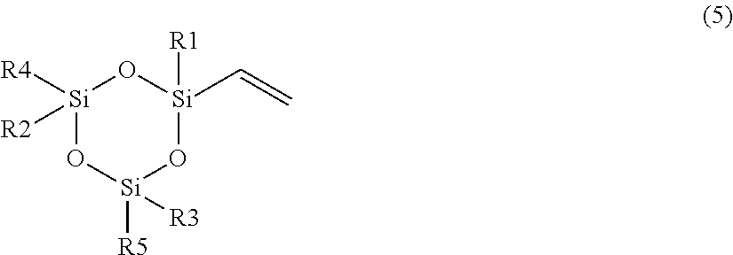
- a vinylcyclotrisiloxane derivative represented by the following formula (5) (wherein R1, R2, R3, R4 and R5 in the formula (5) may be identical or different, and each represent hydrogen, an alkyl group, an alkoxide group, an amino group, an alkene, an alkyne, a phenyl group, a phenol group or the like) may also be used. However, at least one (preferably all) of R1, R2, R3, R4 and R5 is the volatile hydrocarbon group described above.
- the cyclic siloxane compound is an 8-membered ring
- the cyclic siloxane compound is a tetravinylcyclotetrasiloxane monomer represented by the following formula (2) (wherein R1, R2, R3 and R4 in the formula (2) may be identical or different, and each represent hydrogen, an alkyl group, an alkoxide group, an amino group, an alkene, an alkyne, a phenyl group, a phenol group or the like). However, at least one (preferably all) of R1, R2, R3 and R4 is the volatile hydrocarbon group described above.
- a trivinylcyclotetrasiloxane derivative represented by the formula (6) (wherein R1, R2, R3, R4 and R5 in the formula (6) may be identical or different, and each represent hydrogen, an alkyl group, an alkoxide group, an amino group, an alkene, an alkyne, a phenyl group, a phenol group, or the like) may also be used. However, at least one (preferably all) of R1, R2, R3, R4 and R5 is the volatile hydrocarbon group described above.
- a divinylcyclotetrasiloxane derivative represented by formula (7) or (8) (wherein R1, R2, R3, R4, R5 and R6 in the formula (7) or (8) may be identical or different, and each represent hydrogen, an alkyl group, an alkoxide group, an amino group, an alkene, an alkyne, a phenyl group, a phenol group or the like) may also be used. However, at least one (preferably all) of R1, R2, R3, R4, R5 and R6 is the volatile hydrocarbon group described above.
- a vinylcyclotetrasiloxane derivative represented by formula (9) (wherein R1, R2, R3, R4, R5, R6 and R7 in the formula (9) may be identical or different, and each represent hydrogen, an alkyl group, an alkoxide group, an amino group, an alkene, an alkyne, a phenyl group, a phenol group or the like) may also be used. However, at least one (preferably all) of R1, R2, R3, R4, R5, R6 and R7 is the volatile hydrocarbon group described above.
- the cyclic siloxane compound may also be a pentavinylcyclotetrasiloxane derivative, a hexavinylcyclotetrasiloxane derivative, a heptavinylcyclotetrasiloxane derivative, or an octavinylcyclotetrasiloxane derivative.
- the silicon-containing compound that the skeleton includes silicon (Si) and oxygen (O) in a straight chain form.
- the silicon-containing compound has, for example, a structure represented by the following formula (3).
- R1 to R6 may be identical or different, and each represent any one selected from the group consisting of hydrogen, a hydrocarbon group, and an oxidized hydrocarbon group;
- R1 to R4 may be identical or different, and each represent any one selected from the group consisting of hydrogen, a hydrocarbon group, and an oxidized hydrocarbon group;
- R1 to R4 may be identical or different, and each represent any one selected from the group consisting of hydrogen, a hydrocarbon group, and an oxidized hydrocarbon group; or
- R1 to R4 may be identical or different, and each represent any one selected from the group consisting of hydrogen, a hydrocarbon group, and an oxidized hydrocarbon group.
- the silicon-containing compound is, for example, a divinylsiloxanebenzocyclobutene monomer represented by the following formula (10).
- FIG. 1 is a diagram showing the configuration of a film forming apparatus used in the production of a porous insulating film.
- This film forming apparatus has a film forming chamber 10 , an upper electrode 20 , and a lower electrode 30 .
- the upper electrode 20 and the lower electrode 30 are disposed inside the film forming chamber 10 , and are disposed to face each other.
- the upper electrode 20 is a high frequency electrode to which high frequency is applied, and serves as a shower head.
- the process gas for film formation is introduced into the film forming chamber 10 from the upper electrode 20 .
- the lower electrode 30 is a ground electrode, over which a substrate 100 is placed.
- the film forming chamber 10 is also equipped with a ventilation unit that is not shown.
- the process gas includes a noble gas (for example, He gas) containing the cyclic siloxane compound, a noble gas (for example, helium (He) gas) containing the silicon-containing compound, and an inert gas (for example, a noble gas such as He, argon (Ar) or xenon (Xe)).
- a noble gas for example, He gas
- helium (He) gas for example, helium (He) gas
- an inert gas for example, a noble gas such as He, argon (Ar) or xenon (Xe)
- the process gas may also contain an oxidizing gas (for example, N 2 O, O 2 , CO or CO 2 ) in addition to these gases.
- the substrate 100 is placed over the lower electrode 30 of the film forming apparatus shown in FIG. 1 .
- a noble gas containing a cyclic siloxane compound, a noble gas containing a silicon-containing compound, and an inert gas are introduced into the film forming chamber 10 , and high frequency is applied to the upper electrode 20 .
- plasma is generated in the space between the upper electrode 20 and the lower electrode 30 inside the film forming chamber 10 .
- the oxidizing gas mentioned above may be further introduced into the film forming chamber 10 .
- the cyclic siloxane compound is activated while the volatile hydrocarbon group is bonded to the cyclic siloxane, and the cyclic siloxane compound is deposited over the substrate 100 as an insulating substance.
- the silicon-containing compound is activated inside the plasma, and a plurality of cyclic siloxane molecules are bonded to each other through the Si contained in the silicon-containing compound.
- the skeleton of the silicon-containing compound is composed of Si and O
- a plurality of the cyclic siloxane molecules are bonded to each other through the bonding of Si and O (for example, a straight-chained siloxane).
- a straight-chained siloxane bonded to a plurality of cyclic siloxane molecules is likely to be generated.
- the cyclic siloxane constituting the insulating film has a volatile hydrocarbon group bonded thereto.
- the method of applying energy there are a method of applying heat to the substrate 100 and the insulating film, a method of irradiating light such as ultraviolet radiation, a method of irradiating charged particles such as electrons, and the like.
- the temperature of the substrate 100 is set to, for example, 150° C. to 400° C.
- the wavelength of the light is set to 150 to 350 nm.
- the energy of the electrons is set to 0.25 to 20 keV.
- the porous insulating film is, for example, a porous SiOH film, SiCOH film or SiCON film.
- the porous insulating film thus formed contains a plurality of cyclic siloxanes, and the elastic modulus obtained by a nanoindenter is equal to or greater than 5.
- the elastic modulus obtained by a nanoindenter can be measured with high accuracy when, for example, the thickness of the porous insulating film is equal to or greater than 500 nm.
- the molecules of the plurality of cyclic siloxanes are bonded to each other through Si or a straight-chained siloxane.
- the average value of diameter of the pores of the porous insulating film is equal to or less than 1 nm.
- the porous insulating film has a relative permittivity of equal to or less than 2.7, and a C/Si ratio of equal to or greater than 1 and equal to or less than 3 as a ratio of the number of atoms, and preferably equal to or greater than 2 and equal to or less than 3.
- FIG. 2 is an exemplary cross-sectional view of a semiconductor device having a substrate 100 .
- the substrate 100 has a transistor 102 formed thereover.
- An interlayer insulating film 104 and insulating layers 110 , 120 , 130 , 140 and 150 are laminated over the substrate 100 in this sequence.
- the interlayer insulating film 104 and the insulating layer 110 are, for example, silicon oxide films.
- the insulating layer 110 has a conductive pattern 210 buried therein through a barrier metal (not shown).
- the conductive pattern 210 is, for example, a copper (Cu) interconnect.
- the conductive pattern 210 is connected to the transistor 102 , for example, through a contact buried in the interlayer insulating film 104 .
- the insulating layers 120 , 130 and 140 are porous insulating films described above, and the films are respectively buried in conductive patterns 220 , 230 and 240 through barrier metals (not depicted).
- the conductive patterns 220 , 230 and 240 are, for example, Cu interconnects.
- the method of forming the conductive patterns 210 , 220 , 230 and 240 may be either the single Damascene method or the dual Damascene method.
- diffusion preventing film 310 Between the insulating layer 110 and the insulating layer 120 , there is formed a diffusion preventing film 310 . Similarly, diffusion preventing films 320 , 330 and 340 are also formed between the insulating layer 120 and the insulating layer 130 , between the insulating layer 130 and the insulating layer 140 , and between the insulating layer 140 and the insulating layer 150 , respectively.
- FIG. 3 is a graph showing the dependencies on the diameter of pores, respectively of the amount of water absorption in the case of immersing the porous insulating film in water, and of the increment in the relative permittivity before and after the immersion in water.
- the amount of water absorption is decreased with a decrease in the diameter of pores, and the increment of the relative permittivity is also decreased.
- the pore size is controlled to equal to or less than 1 nm, diffusion of moisture, process gas or the like inside the porous insulating film through the pores, can be reduced to a large extent.
- defining the pore size as equal to or less than 1 nm is effective in obtaining high reliability for semiconductor devices because there is an effect of suppressing gas diffusion in the porous insulating film.
- pore refinement since both the cyclic size of the cyclic siloxane, and the pores generated after the detachment of the volatile hydrocarbon group can be adjusted to equal to or less than 1 nm, it is possible to provide a porous insulating film having high reliability.
- a volatile hydrocarbon group is included in a side chain of the cyclic siloxane compound.
- aggregation of the volatile hydrocarbon at the time of deposition of the insulating film is suppressed. Therefore, enlargement of the size of the pores in the porous insulating film is suppressed, and the average value of the diameter of the pores becomes equal to or less than 1 nm.
- the diameter of the pores can be measured by, for example, a small-angle X-ray scattering method.
- the porous insulating film when the pore size is large, the amount of moisture absorption is increased, and thereby the dielectric constant of the porous insulating film is increased. Furthermore, when the amount of moisture absorption is increased, the gas components remaining inside the pores may react with moisture to generate a substance that degenerates the porous insulating film (for example, HF).
- a substance that degenerates the porous insulating film for example, HF
- the diameter of the pores in the porous insulating film can be made small, generation of such problems can be suppressed.
- the molecules of the plurality of cyclic siloxanes are bonded to each other through Si or through the bonding of Si and O (including a straight-chained siloxane). Therefore, the strength of the porous insulating film is increased, and as described above, an elastic modulus obtained by a nanoindenter equal to or greater than 5 is obtained.
- the C/Si ratio in the porous insulating film is equal to or greater than 1 and equal to or less than 3, and preferably equal to or greater than 2 and equal to or less than 3, as a ratio of the number of atoms, even if the porous insulating film is exposed to the plasma during etching or ashing in the subsequent processes, a decrease in the carbon content of the porous insulating film causing an increase in the relative permittivity of the porous insulating film, can be suppressed.
- cyclic siloxane compound a compound was prepared such that a high molecular weight hydrocarbon (the number of carbon atoms being equal to or greater than 2 and equal to or less than 10) was bonded to a side chain of a raw material molecule formed from a 6-membered ring of Si—O having a vinyl group in one of the side chains (trivinylcyclotrisiloxane monomer). Furthermore, dimethyldimethoxysilane (DMDMOS) was prepared as the silicon-containing compound.
- DMDMOS dimethyldimethoxysilane
- the cyclic siloxane compound, the silicon-containing compound and oxygen gas were introduced to a film forming chamber 10 , and thus an insulating film was formed over a silicon substrate. The insulating film over the silicon substrate was converted to a porous insulating film by irradiating the silicon substrate with ultraviolet radiation (Example).
- diethoxymethylsilane DEMS
- an alcohol C 2 H 5 OH, C 2 H 7 OH or the like
- surfactant molecules C 2 H 5 OH, C 2 H 7 OH or the like
- ethers such as vinyl furyl ether, difuryl ether or vinylfuran
- the average values of the diameter of the pores contained in these porous insulating films were measured by a small angle X-ray diffraction method.
- the relative permittivity of the porous insulating film was also measured. The results are presented in FIG. 4 . It was shown from this diagram that the porous insulating film according to the Example has a smaller average value of the diameter of pores even if the relative permittivity is lowered, as compared with the porous insulating film according to the Comparative Example. This is thought to be because, when the relative permittivity is decreased by increasing the amount of pores, aggregation of the porogen does not occur in the Example, while the porogen undergoes aggregation in the Comparative Example, upon the deposition of the insulating film.
Abstract
Description


wherein R1 to R6 may be identical or different, and each represent any one selected from the group consisting of hydrogen, a hydrocarbon group, and an oxidized hydrocarbon group;

wherein R1 to R4 may be identical or different, and each represent any one selected from the group consisting of hydrogen, a hydrocarbon group, and an oxidized hydrocarbon group;

wherein R1 to R4 may be identical or different, and each represent any one selected from the group consisting of hydrogen, a hydrocarbon group, and an oxidized hydrocarbon group; or

wherein R1 to R4 may be identical or different, and each represent any one selected from the group consisting of hydrogen, a hydrocarbon group, and an oxidized hydrocarbon group.

Claims (15)
CnH2n
CnH(2n+2)−2y
CnH2n-2x
CnH2n−2
CnH2n−(2+2x)
CnH2n−4


Priority Applications (1)
| Application Number | Priority Date | Filing Date | Title |
|---|---|---|---|
| US13/363,638 US8937023B2 (en) | 2008-11-18 | 2012-02-01 | Method of manufacturing porous insulating film |
Applications Claiming Priority (4)
| Application Number | Priority Date | Filing Date | Title |
|---|---|---|---|
| JP2008-294090 | 2008-11-18 | ||
| JP2008294090 | 2008-11-18 | ||
| US12/620,913 US8133821B2 (en) | 2008-11-18 | 2009-11-18 | Method of manufacturing porous insulating film, method of manufacturing semiconductor device, and semiconductor device |
| US13/363,638 US8937023B2 (en) | 2008-11-18 | 2012-02-01 | Method of manufacturing porous insulating film |
Related Parent Applications (1)
| Application Number | Title | Priority Date | Filing Date |
|---|---|---|---|
| US12/620,913 Division US8133821B2 (en) | 2008-11-18 | 2009-11-18 | Method of manufacturing porous insulating film, method of manufacturing semiconductor device, and semiconductor device |
Publications (2)
| Publication Number | Publication Date |
|---|---|
| US20120135611A1 US20120135611A1 (en) | 2012-05-31 |
| US8937023B2 true US8937023B2 (en) | 2015-01-20 |
Family
ID=42171331
Family Applications (2)
| Application Number | Title | Priority Date | Filing Date |
|---|---|---|---|
| US12/620,913 Expired - Fee Related US8133821B2 (en) | 2008-11-18 | 2009-11-18 | Method of manufacturing porous insulating film, method of manufacturing semiconductor device, and semiconductor device |
| US13/363,638 Active 2030-11-27 US8937023B2 (en) | 2008-11-18 | 2012-02-01 | Method of manufacturing porous insulating film |
Family Applications Before (1)
| Application Number | Title | Priority Date | Filing Date |
|---|---|---|---|
| US12/620,913 Expired - Fee Related US8133821B2 (en) | 2008-11-18 | 2009-11-18 | Method of manufacturing porous insulating film, method of manufacturing semiconductor device, and semiconductor device |
Country Status (2)
| Country | Link |
|---|---|
| US (2) | US8133821B2 (en) |
| JP (1) | JP2010153824A (en) |
Families Citing this family (6)
| Publication number | Priority date | Publication date | Assignee | Title |
|---|---|---|---|---|
| JP5671253B2 (en) * | 2010-05-07 | 2015-02-18 | ルネサスエレクトロニクス株式会社 | Manufacturing method of semiconductor device |
| JP5654794B2 (en) * | 2010-07-15 | 2015-01-14 | ルネサスエレクトロニクス株式会社 | Manufacturing method of semiconductor device |
| JP2013143392A (en) * | 2012-01-06 | 2013-07-22 | Renesas Electronics Corp | Method of manufacturing porous film, and method of manufacturing semiconductor device |
| TW201348496A (en) * | 2012-02-15 | 2013-12-01 | Renesas Electronics Corp | Methods for making porous insulating films and semiconductor devices including the same |
| US9799557B2 (en) * | 2014-01-22 | 2017-10-24 | Taiwan Semiconductor Manufacturing Co., Ltd. | Semiconductor device structure with metal ring on silicon-on-insulator (SOI) substrate |
| US9209017B2 (en) | 2014-03-26 | 2015-12-08 | International Business Machines Corporation | Advanced ultra low k SiCOH dielectrics prepared by built-in engineered pore size and bonding structured with cyclic organosilicon precursors |
Citations (8)
| Publication number | Priority date | Publication date | Assignee | Title |
|---|---|---|---|---|
| JP2004006822A (en) | 2002-04-17 | 2004-01-08 | Air Products & Chemicals Inc | Method for obtaining and using porogens, porogens-integrated precursor and porous organic silica glass film with low dielectric constant |
| JP2004274052A (en) | 2003-03-04 | 2004-09-30 | Air Products & Chemicals Inc | Mechanical enhancement of high-density porous organic silicate material by uv irradiation |
| WO2005053009A1 (en) | 2003-11-28 | 2005-06-09 | Nec Corporation | Porous insulating film, method for producing same, and semiconductor device using porous insulating film |
| JP2005524983A (en) | 2002-05-08 | 2005-08-18 | アプライド マテリアルズ インコーポレイテッド | Method of curing low dielectric constant film by electron beam |
| JP2005260205A (en) | 2004-02-13 | 2005-09-22 | Matsushita Electric Ind Co Ltd | Method for forming organic/inorganic hybrid insulation film |
| JP2005336391A (en) | 2004-05-28 | 2005-12-08 | Tosoh Corp | Silicon-containing film-forming material and its use |
| JP2007096237A (en) | 2005-09-30 | 2007-04-12 | Tosoh Corp | Si-CONTAINING FILM AND MANUFACTURING METHOD THEREFOR |
| WO2008010591A1 (en) | 2006-07-21 | 2008-01-24 | Nec Corporation | Method for forming porous insulating film |
-
2009
- 2009-11-18 JP JP2009262985A patent/JP2010153824A/en active Pending
- 2009-11-18 US US12/620,913 patent/US8133821B2/en not_active Expired - Fee Related
-
2012
- 2012-02-01 US US13/363,638 patent/US8937023B2/en active Active
Patent Citations (12)
| Publication number | Priority date | Publication date | Assignee | Title |
|---|---|---|---|---|
| JP2004006822A (en) | 2002-04-17 | 2004-01-08 | Air Products & Chemicals Inc | Method for obtaining and using porogens, porogens-integrated precursor and porous organic silica glass film with low dielectric constant |
| JP2007204850A (en) | 2002-04-17 | 2007-08-16 | Air Products & Chemicals Inc | Porogen, porogenated precursor and method for using the same to provide porous organosilica glass film with low dielectric constant |
| US7384471B2 (en) | 2002-04-17 | 2008-06-10 | Air Products And Chemicals, Inc. | Porogens, porogenated precursors and methods for using the same to provide porous organosilica glass films with low dielectric constants |
| US7943195B2 (en) | 2002-04-17 | 2011-05-17 | Air Products And Chemicals, Inc. | Porogens, porogenated precursors and methods for using the same to provide porous organosilica glass films with low dielectric constants |
| JP2005524983A (en) | 2002-05-08 | 2005-08-18 | アプライド マテリアルズ インコーポレイテッド | Method of curing low dielectric constant film by electron beam |
| JP2004274052A (en) | 2003-03-04 | 2004-09-30 | Air Products & Chemicals Inc | Mechanical enhancement of high-density porous organic silicate material by uv irradiation |
| WO2005053009A1 (en) | 2003-11-28 | 2005-06-09 | Nec Corporation | Porous insulating film, method for producing same, and semiconductor device using porous insulating film |
| JP2005260205A (en) | 2004-02-13 | 2005-09-22 | Matsushita Electric Ind Co Ltd | Method for forming organic/inorganic hybrid insulation film |
| JP2005336391A (en) | 2004-05-28 | 2005-12-08 | Tosoh Corp | Silicon-containing film-forming material and its use |
| JP2007096237A (en) | 2005-09-30 | 2007-04-12 | Tosoh Corp | Si-CONTAINING FILM AND MANUFACTURING METHOD THEREFOR |
| WO2008010591A1 (en) | 2006-07-21 | 2008-01-24 | Nec Corporation | Method for forming porous insulating film |
| US20090246538A1 (en) | 2006-07-21 | 2009-10-01 | Hironori Yamamoto | Method of forming a porous insulation film |
Non-Patent Citations (1)
| Title |
|---|
| Notice of Reasons for Rejection mailed Feb. 5, 2013 by the Japanese Patent Office in Japanese Patent Application No. 2009-262985 with English translation of portions within wavy lines. |
Also Published As
| Publication number | Publication date |
|---|---|
| JP2010153824A (en) | 2010-07-08 |
| US8133821B2 (en) | 2012-03-13 |
| US20100123223A1 (en) | 2010-05-20 |
| US20120135611A1 (en) | 2012-05-31 |
Similar Documents
| Publication | Publication Date | Title |
|---|---|---|
| US8937023B2 (en) | Method of manufacturing porous insulating film | |
| US7851384B2 (en) | Method to mitigate impact of UV and E-beam exposure on semiconductor device film properties by use of a bilayer film | |
| US7091137B2 (en) | Bi-layer approach for a hermetic low dielectric constant layer for barrier applications | |
| US6790788B2 (en) | Method of improving stability in low k barrier layers | |
| JP5398258B2 (en) | Dielectric stack and interconnect structure comprising the same | |
| US20050277302A1 (en) | Advanced low dielectric constant barrier layers | |
| US7115534B2 (en) | Dielectric materials to prevent photoresist poisoning | |
| KR101006329B1 (en) | DUV LASER ANNEALING AND STABILIZATION OF SiCOH FILMS | |
| JP5065054B2 (en) | Ultra-low dielectric constant film having controlled biaxial stress and method for producing the same | |
| US20050250346A1 (en) | Process and apparatus for post deposition treatment of low k dielectric materials | |
| KR20130043096A (en) | Ultra low dielectric materials using hybrid precursors containing silicon with organic functional groups by plasma-enhanced chemical vapor deposition | |
| US7288205B2 (en) | Hermetic low dielectric constant layer for barrier applications | |
| JP2007194639A (en) | Sicoh dielectric and its manufacturing method | |
| JP2008527757A5 (en) | ||
| JP5174435B2 (en) | Method for minimizing wet etch undercut and pore sealing ultra-low K (K <2.5) dielectrics | |
| US9698095B2 (en) | Interconnect structure | |
| US7105460B2 (en) | Nitrogen-free dielectric anti-reflective coating and hardmask | |
| JP2007220750A (en) | Forming material of exposure light shielding film, multilayer wiring, manufacturing method thereof, and semiconductor device | |
| KR101106425B1 (en) | Nitrogen-free dielectric anti-reflective coating and hardmask | |
| JP4814054B2 (en) | LAMINATED STRUCTURE, ITS MANUFACTURING METHOD, AND SEMICONDUCTOR DEVICE USING LAMINATE STRUCTURE | |
| US20110223766A1 (en) | Method and apparatus for manufacturing semiconductor device | |
| WO2004104698A2 (en) | Dielectric materials to prevent photoresist poisoning |
Legal Events
| Date | Code | Title | Description |
|---|---|---|---|
| AS | Assignment |
Owner name: NEC ELECTRONICS CORPORATION, JAPAN Free format text: ASSIGNMENT OF ASSIGNORS INTEREST;ASSIGNORS:ITO, FUMINORI;HAYASHI, YOSHIHIRO;REEL/FRAME:027632/0971 Effective date: 20091109 Owner name: RENESAS ELECTRONICS CORPORATION, JAPAN Free format text: CHANGE OF NAME;ASSIGNOR:NEC ELECTRONICS CORPORATION;REEL/FRAME:027633/0161 Effective date: 20100401 |
|
| STCF | Information on status: patent grant |
Free format text: PATENTED CASE |
|
| AS | Assignment |
Owner name: RENESAS ELECTRONICS CORPORATION, JAPAN Free format text: CHANGE OF ADDRESS;ASSIGNOR:RENESAS ELECTRONICS CORPORATION;REEL/FRAME:044928/0001 Effective date: 20150806 |
|
| MAFP | Maintenance fee payment |
Free format text: PAYMENT OF MAINTENANCE FEE, 4TH YEAR, LARGE ENTITY (ORIGINAL EVENT CODE: M1551) Year of fee payment: 4 |
|
| MAFP | Maintenance fee payment |
Free format text: PAYMENT OF MAINTENANCE FEE, 8TH YEAR, LARGE ENTITY (ORIGINAL EVENT CODE: M1552); ENTITY STATUS OF PATENT OWNER: LARGE ENTITY Year of fee payment: 8 |