US8929103B2 - Integrated magnetics with isolated drive circuit - Google Patents
Integrated magnetics with isolated drive circuit Download PDFInfo
- Publication number
- US8929103B2 US8929103B2 US13/427,384 US201213427384A US8929103B2 US 8929103 B2 US8929103 B2 US 8929103B2 US 201213427384 A US201213427384 A US 201213427384A US 8929103 B2 US8929103 B2 US 8929103B2
- Authority
- US
- United States
- Prior art keywords
- primary
- windings
- transformer
- switch
- power
- Prior art date
- Legal status (The legal status is an assumption and is not a legal conclusion. Google has not performed a legal analysis and makes no representation as to the accuracy of the status listed.)
- Active, expires
Links
Images


Classifications
-
- H—ELECTRICITY
- H02—GENERATION; CONVERSION OR DISTRIBUTION OF ELECTRIC POWER
- H02M—APPARATUS FOR CONVERSION BETWEEN AC AND AC, BETWEEN AC AND DC, OR BETWEEN DC AND DC, AND FOR USE WITH MAINS OR SIMILAR POWER SUPPLY SYSTEMS; CONVERSION OF DC OR AC INPUT POWER INTO SURGE OUTPUT POWER; CONTROL OR REGULATION THEREOF
- H02M3/00—Conversion of dc power input into dc power output
- H02M3/22—Conversion of dc power input into dc power output with intermediate conversion into ac
- H02M3/24—Conversion of dc power input into dc power output with intermediate conversion into ac by static converters
- H02M3/28—Conversion of dc power input into dc power output with intermediate conversion into ac by static converters using discharge tubes with control electrode or semiconductor devices with control electrode to produce the intermediate ac
- H02M3/325—Conversion of dc power input into dc power output with intermediate conversion into ac by static converters using discharge tubes with control electrode or semiconductor devices with control electrode to produce the intermediate ac using devices of a triode or a transistor type requiring continuous application of a control signal
- H02M3/335—Conversion of dc power input into dc power output with intermediate conversion into ac by static converters using discharge tubes with control electrode or semiconductor devices with control electrode to produce the intermediate ac using devices of a triode or a transistor type requiring continuous application of a control signal using semiconductor devices only
- H02M3/33569—Conversion of dc power input into dc power output with intermediate conversion into ac by static converters using discharge tubes with control electrode or semiconductor devices with control electrode to produce the intermediate ac using devices of a triode or a transistor type requiring continuous application of a control signal using semiconductor devices only having several active switching elements
- H02M3/33576—Conversion of dc power input into dc power output with intermediate conversion into ac by static converters using discharge tubes with control electrode or semiconductor devices with control electrode to produce the intermediate ac using devices of a triode or a transistor type requiring continuous application of a control signal using semiconductor devices only having several active switching elements having at least one active switching element at the secondary side of an isolation transformer
- H02M3/33592—Conversion of dc power input into dc power output with intermediate conversion into ac by static converters using discharge tubes with control electrode or semiconductor devices with control electrode to produce the intermediate ac using devices of a triode or a transistor type requiring continuous application of a control signal using semiconductor devices only having several active switching elements having at least one active switching element at the secondary side of an isolation transformer having a synchronous rectifier circuit or a synchronous freewheeling circuit at the secondary side of an isolation transformer
-
- H—ELECTRICITY
- H01—ELECTRIC ELEMENTS
- H01F—MAGNETS; INDUCTANCES; TRANSFORMERS; SELECTION OF MATERIALS FOR THEIR MAGNETIC PROPERTIES
- H01F27/00—Details of transformers or inductances, in general
- H01F27/34—Special means for preventing or reducing unwanted electric or magnetic effects, e.g. no-load losses, reactive currents, harmonics, oscillations, leakage fields
- H01F27/38—Auxiliary core members; Auxiliary coils or windings
-
- H—ELECTRICITY
- H02—GENERATION; CONVERSION OR DISTRIBUTION OF ELECTRIC POWER
- H02M—APPARATUS FOR CONVERSION BETWEEN AC AND AC, BETWEEN AC AND DC, OR BETWEEN DC AND DC, AND FOR USE WITH MAINS OR SIMILAR POWER SUPPLY SYSTEMS; CONVERSION OF DC OR AC INPUT POWER INTO SURGE OUTPUT POWER; CONTROL OR REGULATION THEREOF
- H02M1/00—Details of apparatus for conversion
- H02M1/0064—Magnetic structures combining different functions, e.g. storage, filtering or transformation
-
- H—ELECTRICITY
- H02—GENERATION; CONVERSION OR DISTRIBUTION OF ELECTRIC POWER
- H02M—APPARATUS FOR CONVERSION BETWEEN AC AND AC, BETWEEN AC AND DC, OR BETWEEN DC AND DC, AND FOR USE WITH MAINS OR SIMILAR POWER SUPPLY SYSTEMS; CONVERSION OF DC OR AC INPUT POWER INTO SURGE OUTPUT POWER; CONTROL OR REGULATION THEREOF
- H02M1/00—Details of apparatus for conversion
- H02M1/32—Means for protecting converters other than automatic disconnection
- H02M1/34—Snubber circuits
- H02M1/342—Active non-dissipative snubbers
-
- Y—GENERAL TAGGING OF NEW TECHNOLOGICAL DEVELOPMENTS; GENERAL TAGGING OF CROSS-SECTIONAL TECHNOLOGIES SPANNING OVER SEVERAL SECTIONS OF THE IPC; TECHNICAL SUBJECTS COVERED BY FORMER USPC CROSS-REFERENCE ART COLLECTIONS [XRACs] AND DIGESTS
- Y02—TECHNOLOGIES OR APPLICATIONS FOR MITIGATION OR ADAPTATION AGAINST CLIMATE CHANGE
- Y02B—CLIMATE CHANGE MITIGATION TECHNOLOGIES RELATED TO BUILDINGS, e.g. HOUSING, HOUSE APPLIANCES OR RELATED END-USER APPLICATIONS
- Y02B70/00—Technologies for an efficient end-user side electric power management and consumption
- Y02B70/10—Technologies improving the efficiency by using switched-mode power supplies [SMPS], i.e. efficient power electronics conversion e.g. power factor correction or reduction of losses in power supplies or efficient standby modes
-
- Y02B70/1475—
Definitions
- the present invention relates generally to switch-mode power converters. More particularly, the present invention relates to methods and devices for providing an isolated drive circuit integrated into a power transformer or power inductor.
- a switch-mode power converter typically uses an inductor, a transformer, a capacitor, or some combination thereof, as energy storage elements to transfer energy from an input source to an output load in discrete pulses. Additional circuitry is added to maintain a constant voltage or constant current within load limits of the circuit. Using a transformer allows the output to be electrically isolated from the input source.
- One solution is to use direct drive for the synchronous rectifiers with well-controlled timing between the drive signals for the main switches (input side) and the synchronous rectifiers (output side). This solution thus allows for efficient operation of the synchronous rectifiers even at high switching frequencies. Yet another benefit of direct driven synchronous rectifiers is that the drive voltage (gate to source) is constant and independent of input voltage, further improving efficiency over a wide input voltage range.
- Brkovic proposed an improved isolated drive circuit using a drive transformer which provides power and appropriate delays to the primary switches and the synchronous rectifiers.
- This circuit takes advantage of the leakage inductance of the drive transformer windings as well as the input capacitance of the primary switches (MOSFETs) to provide the necessary delays.
- the circuitry further discloses means to disable or enable the primary winding from a condition sensed on the secondary side even with a control and feedback circuit located on the output side.
- FIG. 1 A prior art isolated DC-to-DC converter which employs a double ended DC-to-DC converter having a half-bridge primary circuit and a full-wave secondary circuit employing synchronous rectifiers S 1 and S 2 is shown in FIG. 1 .
- the circuit in FIG. 1 includes switches Q 1 and Q 2 (also called primary controllable power switches), capacitors C 1 and C 2 , a power isolation transformer T 1 , synchronous rectifiers S 1 and S 2 , output inductor L o , and capacitor C o .
- the input voltage V IN is split with filtering capacitors C 1 and C 2 .
- One end of primary winding N p of transformer T 1 is connected to the common node of capacitors C 1 and C 2 while the second end is connected to the common node of switches Q 1 and Q 2 .
- Two secondary windings N S1 and N S2 are center tapped at a common node CT.
- the common node CT is connected to a low pass output filter including inductor L o and capacitor C o connected across the output of the converter and a load.
- the second end of winding N S1 is connected to synchronous rectifier S 1 while the second end of winding N S2 is connected to synchronous rectifier S 2 .
- the polarity of the windings of transformer T 1 is chosen such that when switch Q 1 is on, synchronous rectifier S 1 is on and S 2 is off.
- Switch Q 2 when switch Q 2 is on, synchronous rectifier S 1 is off and S 2 is on.
- Primary switches Q 1 and Q 2 are exemplified as MOSFETs (commonly used today) but may be also realized as IGBTs or other controllable switches.
- the output voltage V OUT is fed into a CONTROL CIRCUIT which generates two output signals OUTA and OUTB having a 180° phase shift that are fed into a SWITCH CONTROL CIRCUIT which generates four signals GQ 1 , GQ 2 , GS 1 and GS 2 for driving switches Q 1 , Q 2 , S 1 and S 2 , respectively.
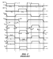
- FIG. 2 The salient waveforms demonstrating operation of the circuitry in the converter shown in FIG. 1 are illustrated in FIG. 2 . It is assumed, for simplicity of explanation, that all voltage waveforms (except OUTA and OUTB) have finite rise and fall times and that all switches have threshold voltages at one-half of the voltage amplitude of the drive signals. Also, the rise and fall times are exaggerated relative to switching period T S for purpose of explanation.
- T S represents the switching period of the converter.
- D represents the duty cycle of the logic signals OUTA and OUTB and is defined as a portion of the half of the switching period T S during which signal OUTA or OUTB are logic high.
- OUTA and OUTB are phase shifted by 180°, and are never at a logic high at the same time.
- FIG. 3 shows a prior art half-bridge converter with practical implementation of a drive transformer T 2 , primary switches Q 1 , Q 2 , as well as synchronous rectifier control circuits.
- a detailed description of the prior art circuit shown in FIG. 4 is described in U.S. Pat. No. 7,102,898 B2 by Brkovic.
- Drive transformer T 2 is implemented as a separate component with windings integrated in the PCB. This implementation has advantages over a solution with windings wound around the magnetic core because it provides better repeatability and control of leakage inductance and capacitance of the drive transformer. Thus, better control of the required timing between the drive signals for primary switches and synchronous rectifiers is achieved.
- the windings of a drive transformer are embedded into a power transformer or inductor so that a separate magnetic core is not needed for the drive transformer.
- the windings of the drive transformer are wound around an outer leg of an E-shaped core, while windings of power transformer or inductor are wound around the center leg.
- Such a winding structure is used to keep the windings of the drive transformer tightly coupled, and at the same time, loosely coupled with the windings of the power transformer or inductor.
- power for driving the power switches after initial turn-on or turn-off is provided from a power transformer or inductor.
- the drive voltage may be clamped in order to be independent of changes in the input voltage.
- the clamped energy is used to power the control and drive circuitry after initial start-up of the converter thus simplifying the bias circuit and reducing power requirements during normal operation of the converter.
- the windings of the drive transformer are wound around both the center and outer legs of the magnetic core of the power transformer or inductor.
- FIG. 1 is a schematic diagram of a prior art circuit using a half-bridge converter and drive transformer with a control and drive circuit referenced to the to the output side of the converter.
- FIG. 2 is a graphical diagram representing salient waveforms derived from several nodes in the prior art circuit of FIG. 1 .
- FIG. 3 is an embodiment of the prior art circuit shown in FIG. 1 , with a drive transformer used to transfer the output of the control circuit CC to the primary switches control circuit PSC.
- FIG. 4 illustrates another embodiment of the prior art circuit of FIG. 1 in which a drive transformer T 2 is used to directly drive the primary side switches and provide the required timing between the drive signals for the primary switches and the synchronous rectifiers.
- FIG. 5 is a schematic diagram of an embodiment of a power converter in accordance with the present invention, having a drive transformer integrated with the power isolation transformer.
- FIG. 6 is an oblique view of a prior art power transformer T 1 as may be used in the converter circuit of FIG. 4 .
- FIG. 7 is an oblique view of a prior art drive transformer T 2 as may be used in the converter circuit of FIG. 4 .
- FIG. 8 is an oblique view of a transformer T 3 as may be used in the converter circuit of FIG. 5 , showing integration of the windings of the power transformer and drive transformer on the same magnetic core according to one aspect of the present invention.
- FIG. 9 is an oblique view of a transformer T 12 as may be used in the converter circuit of FIG. 15 , showing integration of the windings of the power transformer and drive transformer on the same magnetic core according to one aspect of the present invention.
- FIG. 10 is schematic diagram of an active clamp forward converter with a power transformer and drive transformer integrated on one magnetic core according to the present invention, with the control circuit on the output side of the converter.
- FIG. 11 is a schematic diagram of an active clamp forward converter with a power transformer and drive transformer integrated on one magnetic core according to the present invention, with the control circuit on the input side of the converter.
- FIG. 12 is a schematic diagram of an active clamp converter with an output inductor (L 22 ) and drive transformer integrated on one magnetic core according to the present invention, with the control circuit on the input side of the converter.
- FIG. 13 is a schematic diagram of an active clamp converter with an output inductor (L 22 ) and drive transformer integrated on one magnetic core according to the present invention, with the control circuit on the output side of the converter.
- FIG. 14 is an oblique view of one embodiment of an integrated output inductor and drive transformer as may be used in the active clamp converters shown in FIGS. 12 and 13 , according to an aspect of the invention.
- FIG. 15 is a schematic diagram of an embodiment of the power converter circuit of FIG. 3 , but with the power isolation transformer and drive transformer integrated into a single transformer T 12 , according to an aspect of the present invention.
- Coupled means at least either a direct electrical connection between the connected items or an indirect connection through one or more passive or active intermediary devices.
- switching element and “switch” may be used interchangeably and may refer herein to at least: a variety of transistors as known in the art (including but not limited to FET, BJT, IGBT, JFET, etc.), a switching diode, a silicon controlled rectifier (SCR), a diode for alternating current (DIAC), a triode for alternating current (TRIAC), a mechanical single pole/double pole switch (SPDT), or electrical, solid state or reed relays.
- SCR silicon controlled rectifier
- DIAC diode for alternating current
- TRIAC triode for alternating current
- SPDT mechanical single pole/double pole switch
- FET field effect transistor
- BJT bipolar junction transistor
- power converter and “converter” unless otherwise defined with respect to a particular element may be used interchangeably herein and with reference to at least DC-DC, DC-AC, AC-DC, buck, buck-boost, boost, half-bridge, full-bridge, H-bridge or various other forms of power conversion or inversion as known to one of skill in the art.
- Terms such as “providing,” “processing,” “supplying,” “determining,” “calculating” or the like may refer at least to an action of a computer system, computer program, signal processor, logic or alternative analog or digital electronic device that may be transformative of signals represented as physical quantities, whether automatically or manually initiated.
- control circuit may refer to at least a general microprocessor, an application specific integrated circuit (ASIC), a digital signal processor (DSP), a microcontroller, a field programmable gate array, or various alternative blocks of discrete circuitry as known in the art, designed or otherwise programmed to perform or direct the performance of functions as further defined herein.
- ASIC application specific integrated circuit
- DSP digital signal processor
- microcontroller a field programmable gate array
- various alternative blocks of discrete circuitry as known in the art, designed or otherwise programmed to perform or direct the performance of functions as further defined herein.
- general purpose processors it may be understood that such components include or otherwise are functionally linked to non-transitory machine-readable memory media having program instructions residing therein and executable to perform or direct the performance of certain defined functions.
- FIGS. 5 and 8 - 15 various embodiments of a switch-mode power converter having an integrated magnetic structure in accordance with the present invention may be described herein. Where the various figures may describe embodiments sharing various common elements and features with other embodiments, similar elements and features are given the same reference numerals and redundant description thereof may be omitted below.
- FIG. 5 there is shown an embodiment of the present invention used with a half-bridge converter and developed in part from a design as represented in FIG. 4 .
- An important difference between the circuits shown in FIG. 5 and FIG. 4 is the implementation of the drive transformer T 2 .
- FIG. 6 An oblique view of a prior art power transformer T 1 as used in the circuit of FIG. 4 is shown in FIG. 6 .
- a prior art power transformer is typically implemented with a magnetic core having a center leg and two outer legs.
- the primary winding N p is wound around the center leg of the core, as are the center tapped secondary windings N S1 and N S2 .
- the magnetic flux induced by current flow in the winding primary N P circulates through both outer legs of the core, inducing a voltage in windings N S1 and N 32 .
- FIG. 7 An oblique view of a prior art drive transformer T 2 as used in the circuit of FIG. 4 is shown in FIG. 7 , having a construction similar to the power transformer T 1 shown in FIG. 6 .
- This prior art drive transformer is typically implemented with a magnetic core having a center leg and two outer legs. All three windings, N 1 , N 2 and N 3 of the drive transformer are typically wound around the center leg of the core so that they will be tightly coupled.
- FIG. 8 an oblique view of an integrated magnetic structure according to present invention is shown.
- the windings of power transformer T 1 and drive transformer T 2 used in the circuit of FIG. 4 are shown.
- the windings of the power transformer T 1 are wound around the center leg of the core in the same manner as shown in FIG. 6 .
- all windings of the drive transformer T 2 are wound around one of the outer legs of the core, thus preserving tight coupling.
- the windings of the drive transformer, being wound on one of the outer legs of the core of the power transformer are thereby loosely coupled with windings of the power transformer.
- FIG. 10 shows an active clamp forward converter, in which an active clamp circuit (switch Q 11 and capacitor C 11 ) is used to clamp the drain-to-source voltage of the primary switch Q 10 to an acceptable level by allowing the magnetizing current to circulate in the core of transformer T 10 during the reset period.
- An integrated transformer T 10 is used in accordance with the present invention, having power isolation transformer windings N 10 , N 11 and drive transformer windings N 12 , N 13 wound on a single magnetic core, using the winding and core arrangement generally shown in FIG. 8 .
- the control circuit 30 is configured on the output side of the converter.
- the control circuit 30 is functionally coupled to the rectifier control circuit 32 for driving secondary (e.g., synchronous rectifier) switches Q 20 and Q 21 and to the primary switch control circuit 31 used for driving primary side switch Q 10 and active clamp switch Q 11 .
- FIG. 11 shows an active clamp forward converter having a topology similar to that shown in FIG. 10 .
- a transformer T 10 has power isolation transformer windings N 10 , N 11 and drive transformer windings N 14 , N 15 wound on a single magnetic core, using the winding and core arrangement generally shown in FIG. 8 .
- the control circuit 30 is configured on the input side of the converter. The control circuit 30 is functionally coupled to the rectifier control circuit 32 for driving synchronous rectifier switches Q 20 and Q 21 and to the primary switch control circuit 31 used for driving primary side switch Q 10 and active clamp switch Q 11 .
- FIG. 12 shows an active clamp converter similar to those illustrated in FIGS. 10 and 11 , but having a power isolation transformer T 10 and a separate drive transformer T 20 in which the output inductor L 22 and drive transformer windings N 16 and N 17 are integrated on a single magnetic core.
- the control circuit 30 is configured on the input side of the converter.
- the control circuit 30 is functionally coupled to the rectifier control circuit 32 for driving synchronous rectifier switches Q 20 and Q 21 and to the primary switch control circuit 31 used for driving primary side switch Q 10 and active clamp switch Q 11 .
- Feedback isolation circuit 33 couples output voltage Vo to control circuit 30 .
- FIG. 13 illustrates another application of the present invention, showing an active clamp converter with a power isolation transformer T 10 and a separate drive transformer T 21 in which an output inductor L 22 and drive transformer windings N 18 and N 19 are integrated on a single magnetic core.
- the control circuit 30 is configured on the output side of the converter.
- the control circuit 30 is functionally coupled to the rectifier control circuit 32 for driving synchronous rectifier switches Q 20 and Q 21 and to the primary switch control circuit 31 used for driving primary side switch Q 10 and active clamp switch Q 11 .
- FIG. 14 shows an embodiment of an integrated output inductor and drive transformer in accordance with the present invention, as may be used in the active clamp converters shown in FIGS. 12 and 13 .
- FIG. 15 illustrates another application of the present invention, showing the converter circuit of FIG. 3 but with a power isolation transformer primary winding N P2 , split secondary windings N S1 , N S2 , and drive transformer windings 100 and 101 integrated on a single magnetic core of transformer T 12 , as shown in FIG. 9 .
- the converter drive voltage can be clamped to be independent of input voltage, because of the loose coupling between the windings of drive transformer relative to the windings of the power transformer.
- the drive voltage can be also adjusted to be a function of input voltage in applications where it is beneficial.
- energy delivered to the control/drive circuit via a winding can be also controlled or increased by introducing a gap into the center leg or outer leg of the core in a manner as may be understood by one of skill in the art.
- a small gap in the center leg may be needed in case of a very wide input voltage range as well as prolonged operation of the converter with the synchronous rectifiers disabled.
- the windings of the drive transformer can be wound around both the center and outer legs of the magnetic core, in which case the drive voltage for the controllable switches will be more dependent on the input voltage and only a portion of the drive voltage that can be clamped is across the winding wound around the outer leg.
- the present invention can be used in different converter topologies, including half-bridge (symmetric, asymmetric), full-bridge (symmetric, asymmetric), push-pull, forward converter (standard, active clamp, dual transistor), forward-flyback, and many others known in the art.
- the present invention is applicable to all topologies in which the voltage across the windings of the power transformer or inductor has substantially the same waveform with the drive voltage of the various controllable switches.
Landscapes
- Engineering & Computer Science (AREA)
- Power Engineering (AREA)
- Dc-Dc Converters (AREA)
Priority Applications (1)
| Application Number | Priority Date | Filing Date | Title |
|---|---|---|---|
| US13/427,384 US8929103B2 (en) | 2011-03-23 | 2012-03-22 | Integrated magnetics with isolated drive circuit |
Applications Claiming Priority (2)
| Application Number | Priority Date | Filing Date | Title |
|---|---|---|---|
| US201161466824P | 2011-03-23 | 2011-03-23 | |
| US13/427,384 US8929103B2 (en) | 2011-03-23 | 2012-03-22 | Integrated magnetics with isolated drive circuit |
Publications (2)
| Publication Number | Publication Date |
|---|---|
| US20120257421A1 US20120257421A1 (en) | 2012-10-11 |
| US8929103B2 true US8929103B2 (en) | 2015-01-06 |
Family
ID=46880062
Family Applications (1)
| Application Number | Title | Priority Date | Filing Date |
|---|---|---|---|
| US13/427,384 Active 2032-11-28 US8929103B2 (en) | 2011-03-23 | 2012-03-22 | Integrated magnetics with isolated drive circuit |
Country Status (8)
| Country | Link |
|---|---|
| US (1) | US8929103B2 (fr) |
| EP (1) | EP2689522B1 (fr) |
| KR (1) | KR101597885B1 (fr) |
| CN (1) | CN103636108B (fr) |
| ES (1) | ES2768299T3 (fr) |
| HU (1) | HUE048426T2 (fr) |
| PL (1) | PL2689522T3 (fr) |
| WO (1) | WO2012129485A2 (fr) |
Cited By (3)
| Publication number | Priority date | Publication date | Assignee | Title |
|---|---|---|---|---|
| US20140268902A1 (en) * | 2013-03-13 | 2014-09-18 | Apple Inc. | Single stage boost-asymmetric llc |
| US20150109827A1 (en) * | 2013-10-17 | 2015-04-23 | The Governing Council Of The University Of Toronto | Dual Active Bridge With Flyback Mode |
| US20160036337A1 (en) * | 2013-05-21 | 2016-02-04 | Murata Manufacturing Co | Switching power supply apparatus |
Families Citing this family (25)
| Publication number | Priority date | Publication date | Assignee | Title |
|---|---|---|---|---|
| TWI462445B (zh) * | 2012-10-19 | 2014-11-21 | Lite On Technology Corp | 電源轉換裝置 |
| CN102969912B (zh) * | 2012-10-23 | 2014-08-13 | 矽力杰半导体技术(杭州)有限公司 | 控制和驱动电路及方法 |
| US9391529B2 (en) * | 2013-03-04 | 2016-07-12 | Semiconductor Components Industries, Llc | Power converter including a secondary synchronous rectification control module |
| US9537407B2 (en) * | 2013-05-22 | 2017-01-03 | Cree, Inc. | Power supply with standby operation |
| JP6585874B2 (ja) * | 2013-08-26 | 2019-10-02 | ローム株式会社 | 電力供給装置、acアダプタ、および電子機器 |
| CN103777551B (zh) * | 2014-01-24 | 2016-05-18 | 中国北方车辆研究所 | 一种多负载驱动的自动控制与手动控制的切换装置 |
| FI125944B (en) | 2014-02-28 | 2016-04-29 | Jukka Vilhunen | Switched mode converter and electric energy conversion method |
| US9748864B2 (en) * | 2014-06-30 | 2017-08-29 | Mks Instruments, Inc. | Power supply circuits incorporating transformers for combining of power amplifier outputs and isolation of load voltage clamping circuits |
| GB2531350B (en) | 2014-10-17 | 2019-05-15 | Murata Manufacturing Co | High leakage inductance embedded isolation transformer device and method of making the same |
| TWI580168B (zh) * | 2015-05-21 | 2017-04-21 | 立錡科技股份有限公司 | 具有同步控制功能的電源轉換器及其控制方法 |
| WO2017147790A1 (fr) * | 2016-03-01 | 2017-09-08 | Astec International Limited | Alimentations à découpage comprenant des circuits de fixation de niveau côté primaire commandés sur la base de signaux côté secondaire |
| CN106230265A (zh) * | 2016-08-24 | 2016-12-14 | 国网江苏省电力公司电力科学研究院 | 一种电流型dc‑dc隔离转换控制电路 |
| US10003275B2 (en) * | 2016-11-11 | 2018-06-19 | Texas Instruments Incorporated | LLC resonant converter with integrated magnetics |
| KR20180073856A (ko) * | 2016-12-23 | 2018-07-03 | 현대엘리베이터주식회사 | 절연된 전원을 이용한 스위칭 구동회로 |
| CN107453610B (zh) | 2017-07-31 | 2020-01-24 | 西安矽力杰半导体技术有限公司 | 反激式变换器及其有源箝位控制电路和有源箝位控制方法 |
| CN107517005A (zh) * | 2017-09-22 | 2017-12-26 | 厦门玛司特电子工业有限公司 | 一种高低压同步有源钳位转换电路及其控制方法 |
| US10872753B2 (en) * | 2018-07-25 | 2020-12-22 | Agilent Technologies, Inc. | Precision high voltage power supply utilizing feedback through return side output |
| KR102016966B1 (ko) * | 2018-10-30 | 2019-09-02 | 청주대학교 산학협력단 | 플라이백 컨버터 |
| US10425080B1 (en) * | 2018-11-06 | 2019-09-24 | Crane Electronics, Inc. | Magnetic peak current mode control for radiation tolerant active driven synchronous power converters |
| CN112238785B (zh) | 2019-07-16 | 2022-03-04 | 宁德时代新能源科技股份有限公司 | 电池管理系统的唤醒方法和唤醒系统 |
| CN112238786B (zh) | 2019-07-16 | 2022-02-18 | 宁德时代新能源科技股份有限公司 | 常电提供系统和常电提供方法 |
| CN110957919A (zh) * | 2019-11-14 | 2020-04-03 | 北京新雷能科技股份有限公司 | 一种半桥磁集成驱动电路和dc/dc电源 |
| US11742767B2 (en) * | 2020-06-26 | 2023-08-29 | Maxim Integrated Products, Inc. | Flux-corrected switching power converters |
| CN113346764A (zh) * | 2021-05-13 | 2021-09-03 | 西安交通大学 | 一种基于高频磁耦合模块的中压变流器拓扑结构 |
| CN114301284B (zh) * | 2021-12-24 | 2023-09-08 | 有方(合肥)医疗科技有限公司 | X射线球管灯丝加热控制装置、方法及ct系统 |
Citations (21)
| Publication number | Priority date | Publication date | Assignee | Title |
|---|---|---|---|---|
| US4821163A (en) | 1987-12-23 | 1989-04-11 | Bloom Gordon E | Start-up circuit for an integrated-magnetic power converter |
| US5155676A (en) * | 1991-11-01 | 1992-10-13 | International Business Machines Corporation | Gapped/ungapped magnetic core |
| US5784266A (en) | 1996-06-14 | 1998-07-21 | Virginia Power Technologies, Inc | Single magnetic low loss high frequency converter |
| US5907481A (en) | 1997-10-31 | 1999-05-25 | Telefonaktiebolaget Lm Ericsson | Double ended isolated D.C.--D.C. converter |
| US6111769A (en) * | 1999-09-24 | 2000-08-29 | Ericsson, Inc. | External driving circuit for bridge type synchronous rectification |
| US20010024373A1 (en) | 2000-03-24 | 2001-09-27 | Slobodan Cuk | Lossless switching dc to dc converter with dc transformer |
| US20020110005A1 (en) * | 2001-02-09 | 2002-08-15 | Hengchun Mao | Power converter including circuits for improved operational contol of synchronous rectifiers therein |
| US6788553B1 (en) * | 2001-12-28 | 2004-09-07 | Broadband Telcom Power, Inc. | Switching-mode power converter with complementary synchronous rectification |
| US6804125B2 (en) | 2001-02-01 | 2004-10-12 | Di/Dt Inc. | Isolated drive circuitry used in switch-mode power converters |
| US20040257837A1 (en) * | 2003-01-24 | 2004-12-23 | Ming Xu | Self-driven circuit for synchronous rectifier DC/DC converter |
| US20050041441A1 (en) * | 2003-08-18 | 2005-02-24 | Murata Manfacturing Co., Ltd. | Switching electric source device |
| US20050068792A1 (en) * | 2003-09-30 | 2005-03-31 | Masayuki Yasumura | Switching power supply circuit |
| US6888728B2 (en) * | 2001-05-25 | 2005-05-03 | Tdk Corporation | Switching power supply unit |
| US7002818B2 (en) * | 2003-12-19 | 2006-02-21 | Silent Power, Inc. | Power converter with improved output switching timing |
| US20060077694A1 (en) * | 2004-10-07 | 2006-04-13 | Ivan Meszlenyi | Pulse transition time modulation power converter |
| US7102898B2 (en) | 2001-02-01 | 2006-09-05 | Di/Dt, Inc. | Isolated drive circuitry used in switch-mode power converters |
| CN201266888Y (zh) | 2008-10-15 | 2009-07-01 | 北京新雷能有限责任公司 | 一种集成磁元件的直流变换器 |
| US20090196076A1 (en) | 2008-01-31 | 2009-08-06 | Stmicroelectronics, Inc. | Integrated base driver and switching windings for an esbt power driver |
| US20090230776A1 (en) | 2008-03-17 | 2009-09-17 | Asic Advantage Inc. | Integrated multi-transformer |
| US20090244931A1 (en) * | 2008-03-27 | 2009-10-01 | Power-One, Inc. | Method and apparatus for providing an initial bias and enable signal for a power converter |
| US7876191B2 (en) | 2005-02-23 | 2011-01-25 | Flextronics International Usa, Inc. | Power converter employing a tapped inductor and integrated magnetics and method of operating the same |
Family Cites Families (4)
| Publication number | Priority date | Publication date | Assignee | Title |
|---|---|---|---|---|
| JP2000260639A (ja) * | 1999-03-11 | 2000-09-22 | Murata Mfg Co Ltd | コイル装置およびこれを用いたスイッチング電源装置 |
| CN1295853C (zh) * | 2001-02-09 | 2007-01-17 | 精电科技公司 | 包括用于对同步整流器进行控制的电路的电源变换器 |
| WO2007069403A1 (fr) * | 2005-12-16 | 2007-06-21 | Murata Manufacturing Co., Ltd. | Transformateur composite et alimentation à découpage isolée |
| CN101517878B (zh) * | 2006-10-02 | 2012-02-08 | 株式会社村田制作所 | 双端绝缘型dc-dc转换器 |
-
2012
- 2012-03-22 US US13/427,384 patent/US8929103B2/en active Active
- 2012-03-23 CN CN201280024672.5A patent/CN103636108B/zh active Active
- 2012-03-23 KR KR1020137027995A patent/KR101597885B1/ko active IP Right Grant
- 2012-03-23 HU HUE12761425A patent/HUE048426T2/hu unknown
- 2012-03-23 ES ES12761425T patent/ES2768299T3/es active Active
- 2012-03-23 WO PCT/US2012/030301 patent/WO2012129485A2/fr active Application Filing
- 2012-03-23 EP EP12761425.3A patent/EP2689522B1/fr active Active
- 2012-03-23 PL PL12761425T patent/PL2689522T3/pl unknown
Patent Citations (21)
| Publication number | Priority date | Publication date | Assignee | Title |
|---|---|---|---|---|
| US4821163A (en) | 1987-12-23 | 1989-04-11 | Bloom Gordon E | Start-up circuit for an integrated-magnetic power converter |
| US5155676A (en) * | 1991-11-01 | 1992-10-13 | International Business Machines Corporation | Gapped/ungapped magnetic core |
| US5784266A (en) | 1996-06-14 | 1998-07-21 | Virginia Power Technologies, Inc | Single magnetic low loss high frequency converter |
| US5907481A (en) | 1997-10-31 | 1999-05-25 | Telefonaktiebolaget Lm Ericsson | Double ended isolated D.C.--D.C. converter |
| US6111769A (en) * | 1999-09-24 | 2000-08-29 | Ericsson, Inc. | External driving circuit for bridge type synchronous rectification |
| US20010024373A1 (en) | 2000-03-24 | 2001-09-27 | Slobodan Cuk | Lossless switching dc to dc converter with dc transformer |
| US7102898B2 (en) | 2001-02-01 | 2006-09-05 | Di/Dt, Inc. | Isolated drive circuitry used in switch-mode power converters |
| US6804125B2 (en) | 2001-02-01 | 2004-10-12 | Di/Dt Inc. | Isolated drive circuitry used in switch-mode power converters |
| US20020110005A1 (en) * | 2001-02-09 | 2002-08-15 | Hengchun Mao | Power converter including circuits for improved operational contol of synchronous rectifiers therein |
| US6888728B2 (en) * | 2001-05-25 | 2005-05-03 | Tdk Corporation | Switching power supply unit |
| US6788553B1 (en) * | 2001-12-28 | 2004-09-07 | Broadband Telcom Power, Inc. | Switching-mode power converter with complementary synchronous rectification |
| US20040257837A1 (en) * | 2003-01-24 | 2004-12-23 | Ming Xu | Self-driven circuit for synchronous rectifier DC/DC converter |
| US20050041441A1 (en) * | 2003-08-18 | 2005-02-24 | Murata Manfacturing Co., Ltd. | Switching electric source device |
| US20050068792A1 (en) * | 2003-09-30 | 2005-03-31 | Masayuki Yasumura | Switching power supply circuit |
| US7002818B2 (en) * | 2003-12-19 | 2006-02-21 | Silent Power, Inc. | Power converter with improved output switching timing |
| US20060077694A1 (en) * | 2004-10-07 | 2006-04-13 | Ivan Meszlenyi | Pulse transition time modulation power converter |
| US7876191B2 (en) | 2005-02-23 | 2011-01-25 | Flextronics International Usa, Inc. | Power converter employing a tapped inductor and integrated magnetics and method of operating the same |
| US20090196076A1 (en) | 2008-01-31 | 2009-08-06 | Stmicroelectronics, Inc. | Integrated base driver and switching windings for an esbt power driver |
| US20090230776A1 (en) | 2008-03-17 | 2009-09-17 | Asic Advantage Inc. | Integrated multi-transformer |
| US20090244931A1 (en) * | 2008-03-27 | 2009-10-01 | Power-One, Inc. | Method and apparatus for providing an initial bias and enable signal for a power converter |
| CN201266888Y (zh) | 2008-10-15 | 2009-07-01 | 北京新雷能有限责任公司 | 一种集成磁元件的直流变换器 |
Non-Patent Citations (1)
| Title |
|---|
| International Search Report and Written Opinion, dated Oct. 25, 2012, 10 pp., in corresponding International Application No. PCT/US2012/030301. |
Cited By (6)
| Publication number | Priority date | Publication date | Assignee | Title |
|---|---|---|---|---|
| US20140268902A1 (en) * | 2013-03-13 | 2014-09-18 | Apple Inc. | Single stage boost-asymmetric llc |
| US9325249B2 (en) * | 2013-03-13 | 2016-04-26 | Apple Inc. | Single stage boost-asymmetric LLC |
| US20160036337A1 (en) * | 2013-05-21 | 2016-02-04 | Murata Manufacturing Co | Switching power supply apparatus |
| US9748851B2 (en) * | 2013-05-21 | 2017-08-29 | Murata Manufacturing Co., Ltd. | Switching power supply apparatus with snubber circuit |
| US20150109827A1 (en) * | 2013-10-17 | 2015-04-23 | The Governing Council Of The University Of Toronto | Dual Active Bridge With Flyback Mode |
| US9673719B2 (en) * | 2013-10-17 | 2017-06-06 | The Governing Council Of The University Of Toronto | Dual Active Bridge with flyback mode |
Also Published As
| Publication number | Publication date |
|---|---|
| CN103636108B (zh) | 2016-10-12 |
| ES2768299T3 (es) | 2020-06-22 |
| PL2689522T3 (pl) | 2020-06-01 |
| WO2012129485A2 (fr) | 2012-09-27 |
| WO2012129485A3 (fr) | 2012-12-27 |
| HUE048426T2 (hu) | 2020-08-28 |
| US20120257421A1 (en) | 2012-10-11 |
| EP2689522A2 (fr) | 2014-01-29 |
| EP2689522B1 (fr) | 2019-11-13 |
| EP2689522A4 (fr) | 2015-07-29 |
| KR20140015494A (ko) | 2014-02-06 |
| CN103636108A (zh) | 2014-03-12 |
| KR101597885B1 (ko) | 2016-02-25 |
Similar Documents
| Publication | Publication Date | Title |
|---|---|---|
| US8929103B2 (en) | Integrated magnetics with isolated drive circuit | |
| US9812977B2 (en) | Resonant converters with an improved voltage regulation range | |
| KR100691929B1 (ko) | 플로팅 게이트를 가진 동기 정류기에 대한 일반적인 자기 구동 동기 정류 방식 | |
| US6760235B2 (en) | Soft start for a synchronous rectifier in a power converter | |
| US8966294B2 (en) | Clamp circuits for power converters | |
| US20090196072A1 (en) | Phase-shifted dual-bridge DC/DC converter with wide-range ZVS and zero circulating current | |
| US6344768B1 (en) | Full-bridge DC-to-DC converter having an unipolar gate drive | |
| JP2019106839A (ja) | Dc/dcコンバータ | |
| US9837920B2 (en) | Commutation current steering method in a zero volt switching power converter using a synchronous rectifier | |
| CN107431438B (zh) | 包括基于次级侧信号受控的初级侧箝位电路的开关模式电源 | |
| Song et al. | Current-fed dual-bridge DC–DC converter | |
| CN104038037B (zh) | 辅助再充电 | |
| US9577540B1 (en) | Multi-stage flyback converter for wide input voltage range applications | |
| CN102239628A (zh) | 用于减少来自环振荡的emi的切换功率转换器及其控制方法 | |
| KR102129872B1 (ko) | 양방향 능동 정류 브릿지를 이용하는 전력 변환기 | |
| US6859372B2 (en) | Bridge-buck converter with self-driven synchronous rectifiers | |
| US20160036337A1 (en) | Switching power supply apparatus | |
| TWI580166B (zh) | 交錯式升壓轉換器 | |
| KR20160011497A (ko) | 고효율 역률 개선용 단일단 ac/dc 컨버터 | |
| US11973440B2 (en) | Isolated DC/DC converter with secondary-side full bridge diode rectifier and asymmetrical auxiliary capacitor | |
| KR101444594B1 (ko) | 위상 천이 풀브리지 컨버터 | |
| KR20150070898A (ko) | 직류-직류 컨버터 및 이의 스위칭 방법 | |
| JP2018061336A (ja) | 双方向絶縁型dc/dcコンバータ | |
| KR20220101673A (ko) | 직류 전력 변환기 | |
| KR102077825B1 (ko) | 부스트 컨버터 |
Legal Events
| Date | Code | Title | Description |
|---|---|---|---|
| AS | Assignment |
Owner name: BANK OF AMERICA, N.A., AS ADMINISTRATIVE AGENT, IL Free format text: PATENT SECURITY AGREEMENT;ASSIGNOR:POWER-ONE, INC.;REEL/FRAME:029759/0460 Effective date: 20130130 |
|
| AS | Assignment |
Owner name: POWER-ONE, INC., CALIFORNIA Free format text: ASSIGNMENT OF ASSIGNORS INTEREST;ASSIGNOR:BRKOVIC, MILIVOJE;REEL/FRAME:032510/0564 Effective date: 20120603 |
|
| AS | Assignment |
Owner name: POWER-ONE, INC., CALIFORNIA Free format text: RELEASE BY SECURED PARTY;ASSIGNOR:BANK OF AMERICA, N.A., AS ADMINISTRATIVE AGENT;REEL/FRAME:032821/0013 Effective date: 20130722 |
|
| AS | Assignment |
Owner name: PAI CAPITAL LLC, CALIFORNIA Free format text: NUNC PRO TUNC ASSIGNMENT;ASSIGNOR:POWER-ONE, INC.;REEL/FRAME:033227/0968 Effective date: 20140604 |
|
| STCF | Information on status: patent grant |
Free format text: PATENTED CASE |
|
| AS | Assignment |
Owner name: BEL POWER SOLUTIONS INC., CALIFORNIA Free format text: ASSIGNMENT OF ASSIGNORS INTEREST;ASSIGNOR:PAI CAPITAL LLC;REEL/FRAME:043274/0849 Effective date: 20170615 |
|
| MAFP | Maintenance fee payment |
Free format text: PAYMENT OF MAINTENANCE FEE, 4TH YEAR, LARGE ENTITY (ORIGINAL EVENT CODE: M1551) Year of fee payment: 4 |
|
| AS | Assignment |
Owner name: KEYBANK NATIONAL ASSOCIATION, AS ADMINISTRATIVE AGENT, OHIO Free format text: SECURITY INTEREST;ASSIGNOR:BEL FUSE INC.;REEL/FRAME:058917/0452 Effective date: 20210902 |
|
| MAFP | Maintenance fee payment |
Free format text: PAYMENT OF MAINTENANCE FEE, 8TH YEAR, LARGE ENTITY (ORIGINAL EVENT CODE: M1552); ENTITY STATUS OF PATENT OWNER: LARGE ENTITY Year of fee payment: 8 |