US8902135B2 - Pixel structure of organic electroluminescence device - Google Patents
Pixel structure of organic electroluminescence device Download PDFInfo
- Publication number
- US8902135B2 US8902135B2 US13/366,270 US201213366270A US8902135B2 US 8902135 B2 US8902135 B2 US 8902135B2 US 201213366270 A US201213366270 A US 201213366270A US 8902135 B2 US8902135 B2 US 8902135B2
- Authority
- US
- United States
- Prior art keywords
- gate
- disposed
- line
- source
- electrically connected
- Prior art date
- Legal status (The legal status is an assumption and is not a legal conclusion. Google has not performed a legal analysis and makes no representation as to the accuracy of the status listed.)
- Active, expires
Links
Images


Classifications
-
- H—ELECTRICITY
- H10—SEMICONDUCTOR DEVICES; ELECTRIC SOLID-STATE DEVICES NOT OTHERWISE PROVIDED FOR
- H10K—ORGANIC ELECTRIC SOLID-STATE DEVICES
- H10K59/00—Integrated devices, or assemblies of multiple devices, comprising at least one organic light-emitting element covered by group H10K50/00
- H10K59/30—Devices specially adapted for multicolour light emission
- H10K59/32—Stacked devices having two or more layers, each emitting at different wavelengths
-
- G—PHYSICS
- G09—EDUCATION; CRYPTOGRAPHY; DISPLAY; ADVERTISING; SEALS
- G09G—ARRANGEMENTS OR CIRCUITS FOR CONTROL OF INDICATING DEVICES USING STATIC MEANS TO PRESENT VARIABLE INFORMATION
- G09G3/00—Control arrangements or circuits, of interest only in connection with visual indicators other than cathode-ray tubes
- G09G3/20—Control arrangements or circuits, of interest only in connection with visual indicators other than cathode-ray tubes for presentation of an assembly of a number of characters, e.g. a page, by composing the assembly by combination of individual elements arranged in a matrix no fixed position being assigned to or needed to be assigned to the individual characters or partial characters
- G09G3/22—Control arrangements or circuits, of interest only in connection with visual indicators other than cathode-ray tubes for presentation of an assembly of a number of characters, e.g. a page, by composing the assembly by combination of individual elements arranged in a matrix no fixed position being assigned to or needed to be assigned to the individual characters or partial characters using controlled light sources
- G09G3/30—Control arrangements or circuits, of interest only in connection with visual indicators other than cathode-ray tubes for presentation of an assembly of a number of characters, e.g. a page, by composing the assembly by combination of individual elements arranged in a matrix no fixed position being assigned to or needed to be assigned to the individual characters or partial characters using controlled light sources using electroluminescent panels
- G09G3/32—Control arrangements or circuits, of interest only in connection with visual indicators other than cathode-ray tubes for presentation of an assembly of a number of characters, e.g. a page, by composing the assembly by combination of individual elements arranged in a matrix no fixed position being assigned to or needed to be assigned to the individual characters or partial characters using controlled light sources using electroluminescent panels semiconductive, e.g. using light-emitting diodes [LED]
- G09G3/3208—Control arrangements or circuits, of interest only in connection with visual indicators other than cathode-ray tubes for presentation of an assembly of a number of characters, e.g. a page, by composing the assembly by combination of individual elements arranged in a matrix no fixed position being assigned to or needed to be assigned to the individual characters or partial characters using controlled light sources using electroluminescent panels semiconductive, e.g. using light-emitting diodes [LED] organic, e.g. using organic light-emitting diodes [OLED]
- G09G3/3225—Control arrangements or circuits, of interest only in connection with visual indicators other than cathode-ray tubes for presentation of an assembly of a number of characters, e.g. a page, by composing the assembly by combination of individual elements arranged in a matrix no fixed position being assigned to or needed to be assigned to the individual characters or partial characters using controlled light sources using electroluminescent panels semiconductive, e.g. using light-emitting diodes [LED] organic, e.g. using organic light-emitting diodes [OLED] using an active matrix
- G09G3/3258—Control arrangements or circuits, of interest only in connection with visual indicators other than cathode-ray tubes for presentation of an assembly of a number of characters, e.g. a page, by composing the assembly by combination of individual elements arranged in a matrix no fixed position being assigned to or needed to be assigned to the individual characters or partial characters using controlled light sources using electroluminescent panels semiconductive, e.g. using light-emitting diodes [LED] organic, e.g. using organic light-emitting diodes [OLED] using an active matrix with pixel circuitry controlling the voltage across the light-emitting element
-
- G—PHYSICS
- G06—COMPUTING; CALCULATING OR COUNTING
- G06F—ELECTRIC DIGITAL DATA PROCESSING
- G06F3/00—Input arrangements for transferring data to be processed into a form capable of being handled by the computer; Output arrangements for transferring data from processing unit to output unit, e.g. interface arrangements
- G06F3/01—Input arrangements or combined input and output arrangements for interaction between user and computer
- G06F3/03—Arrangements for converting the position or the displacement of a member into a coded form
- G06F3/041—Digitisers, e.g. for touch screens or touch pads, characterised by the transducing means
- G06F3/0412—Digitisers structurally integrated in a display
-
- G—PHYSICS
- G06—COMPUTING; CALCULATING OR COUNTING
- G06F—ELECTRIC DIGITAL DATA PROCESSING
- G06F3/00—Input arrangements for transferring data to be processed into a form capable of being handled by the computer; Output arrangements for transferring data from processing unit to output unit, e.g. interface arrangements
- G06F3/01—Input arrangements or combined input and output arrangements for interaction between user and computer
- G06F3/03—Arrangements for converting the position or the displacement of a member into a coded form
- G06F3/041—Digitisers, e.g. for touch screens or touch pads, characterised by the transducing means
- G06F3/042—Digitisers, e.g. for touch screens or touch pads, characterised by the transducing means by opto-electronic means
- G06F3/0421—Digitisers, e.g. for touch screens or touch pads, characterised by the transducing means by opto-electronic means by interrupting or reflecting a light beam, e.g. optical touch-screen
-
- H—ELECTRICITY
- H10—SEMICONDUCTOR DEVICES; ELECTRIC SOLID-STATE DEVICES NOT OTHERWISE PROVIDED FOR
- H10K—ORGANIC ELECTRIC SOLID-STATE DEVICES
- H10K50/00—Organic light-emitting devices
- H10K50/10—OLEDs or polymer light-emitting diodes [PLED]
- H10K50/11—OLEDs or polymer light-emitting diodes [PLED] characterised by the electroluminescent [EL] layers
- H10K50/125—OLEDs or polymer light-emitting diodes [PLED] characterised by the electroluminescent [EL] layers specially adapted for multicolour light emission, e.g. for emitting white light
- H10K50/13—OLEDs or polymer light-emitting diodes [PLED] characterised by the electroluminescent [EL] layers specially adapted for multicolour light emission, e.g. for emitting white light comprising stacked EL layers within one EL unit
-
- H—ELECTRICITY
- H10—SEMICONDUCTOR DEVICES; ELECTRIC SOLID-STATE DEVICES NOT OTHERWISE PROVIDED FOR
- H10K—ORGANIC ELECTRIC SOLID-STATE DEVICES
- H10K50/00—Organic light-emitting devices
- H10K50/80—Constructional details
- H10K50/805—Electrodes
-
- H—ELECTRICITY
- H10—SEMICONDUCTOR DEVICES; ELECTRIC SOLID-STATE DEVICES NOT OTHERWISE PROVIDED FOR
- H10K—ORGANIC ELECTRIC SOLID-STATE DEVICES
- H10K50/00—Organic light-emitting devices
- H10K50/80—Constructional details
- H10K50/805—Electrodes
- H10K50/81—Anodes
- H10K50/818—Reflective anodes, e.g. ITO combined with thick metallic layers
-
- H—ELECTRICITY
- H10—SEMICONDUCTOR DEVICES; ELECTRIC SOLID-STATE DEVICES NOT OTHERWISE PROVIDED FOR
- H10K—ORGANIC ELECTRIC SOLID-STATE DEVICES
- H10K50/00—Organic light-emitting devices
- H10K50/80—Constructional details
- H10K50/805—Electrodes
- H10K50/82—Cathodes
- H10K50/828—Transparent cathodes, e.g. comprising thin metal layers
-
- H—ELECTRICITY
- H10—SEMICONDUCTOR DEVICES; ELECTRIC SOLID-STATE DEVICES NOT OTHERWISE PROVIDED FOR
- H10K—ORGANIC ELECTRIC SOLID-STATE DEVICES
- H10K59/00—Integrated devices, or assemblies of multiple devices, comprising at least one organic light-emitting element covered by group H10K50/00
- H10K59/10—OLED displays
- H10K59/12—Active-matrix OLED [AMOLED] displays
- H10K59/121—Active-matrix OLED [AMOLED] displays characterised by the geometry or disposition of pixel elements
- H10K59/1216—Active-matrix OLED [AMOLED] displays characterised by the geometry or disposition of pixel elements the pixel elements being capacitors
-
- H—ELECTRICITY
- H10—SEMICONDUCTOR DEVICES; ELECTRIC SOLID-STATE DEVICES NOT OTHERWISE PROVIDED FOR
- H10K—ORGANIC ELECTRIC SOLID-STATE DEVICES
- H10K59/00—Integrated devices, or assemblies of multiple devices, comprising at least one organic light-emitting element covered by group H10K50/00
- H10K59/10—OLED displays
- H10K59/12—Active-matrix OLED [AMOLED] displays
- H10K59/123—Connection of the pixel electrodes to the thin film transistors [TFT]
-
- H—ELECTRICITY
- H10—SEMICONDUCTOR DEVICES; ELECTRIC SOLID-STATE DEVICES NOT OTHERWISE PROVIDED FOR
- H10K—ORGANIC ELECTRIC SOLID-STATE DEVICES
- H10K59/00—Integrated devices, or assemblies of multiple devices, comprising at least one organic light-emitting element covered by group H10K50/00
- H10K59/10—OLED displays
- H10K59/12—Active-matrix OLED [AMOLED] displays
- H10K59/126—Shielding, e.g. light-blocking means over the TFTs
-
- H—ELECTRICITY
- H10—SEMICONDUCTOR DEVICES; ELECTRIC SOLID-STATE DEVICES NOT OTHERWISE PROVIDED FOR
- H10K—ORGANIC ELECTRIC SOLID-STATE DEVICES
- H10K59/00—Integrated devices, or assemblies of multiple devices, comprising at least one organic light-emitting element covered by group H10K50/00
- H10K59/10—OLED displays
- H10K59/12—Active-matrix OLED [AMOLED] displays
- H10K59/13—Active-matrix OLED [AMOLED] displays comprising photosensors that control luminance
-
- H—ELECTRICITY
- H10—SEMICONDUCTOR DEVICES; ELECTRIC SOLID-STATE DEVICES NOT OTHERWISE PROVIDED FOR
- H10K—ORGANIC ELECTRIC SOLID-STATE DEVICES
- H10K59/00—Integrated devices, or assemblies of multiple devices, comprising at least one organic light-emitting element covered by group H10K50/00
- H10K59/30—Devices specially adapted for multicolour light emission
- H10K59/35—Devices specially adapted for multicolour light emission comprising red-green-blue [RGB] subpixels
- H10K59/353—Devices specially adapted for multicolour light emission comprising red-green-blue [RGB] subpixels characterised by the geometrical arrangement of the RGB subpixels
-
- H—ELECTRICITY
- H10—SEMICONDUCTOR DEVICES; ELECTRIC SOLID-STATE DEVICES NOT OTHERWISE PROVIDED FOR
- H10K—ORGANIC ELECTRIC SOLID-STATE DEVICES
- H10K59/00—Integrated devices, or assemblies of multiple devices, comprising at least one organic light-emitting element covered by group H10K50/00
- H10K59/40—OLEDs integrated with touch screens
-
- G—PHYSICS
- G06—COMPUTING; CALCULATING OR COUNTING
- G06F—ELECTRIC DIGITAL DATA PROCESSING
- G06F2203/00—Indexing scheme relating to G06F3/00 - G06F3/048
- G06F2203/041—Indexing scheme relating to G06F3/041 - G06F3/045
- G06F2203/04103—Manufacturing, i.e. details related to manufacturing processes specially suited for touch sensitive devices
-
- G—PHYSICS
- G09—EDUCATION; CRYPTOGRAPHY; DISPLAY; ADVERTISING; SEALS
- G09G—ARRANGEMENTS OR CIRCUITS FOR CONTROL OF INDICATING DEVICES USING STATIC MEANS TO PRESENT VARIABLE INFORMATION
- G09G2300/00—Aspects of the constitution of display devices
- G09G2300/04—Structural and physical details of display devices
- G09G2300/0421—Structural details of the set of electrodes
- G09G2300/0426—Layout of electrodes and connections
-
- G—PHYSICS
- G09—EDUCATION; CRYPTOGRAPHY; DISPLAY; ADVERTISING; SEALS
- G09G—ARRANGEMENTS OR CIRCUITS FOR CONTROL OF INDICATING DEVICES USING STATIC MEANS TO PRESENT VARIABLE INFORMATION
- G09G2320/00—Control of display operating conditions
- G09G2320/02—Improving the quality of display appearance
- G09G2320/029—Improving the quality of display appearance by monitoring one or more pixels in the display panel, e.g. by monitoring a fixed reference pixel
- G09G2320/0295—Improving the quality of display appearance by monitoring one or more pixels in the display panel, e.g. by monitoring a fixed reference pixel by monitoring each display pixel
Definitions
- the present invention relates to a pixel structure. More particularly, the present invention relates to a pixel structure of an organic electroluminescence device.
- the organic electroluminescence device As an emissive device, the organic electroluminescence device has the advantages of no view angle limit, low fabrication cost, high response speed (about more than one hundred times faster than the response speed of the liquid crystal), power saving, adaptability to direct current driving in portable devices, broad operating temperature range, light weight, as well as providing miniature and low-profile design Therefore, the organic electroluminescence device has a great development potential and is expected to be the next generation of flat panel display.
- touch sensing display panels have been introduced as input devices in replacement of conventional keyboards or mice.
- a touch sensing display panel capable of performing both a touch sensing function and a display function is one of the most popular products at present.
- the present invention is directed to a pixel structure of an organic electroluminescence device having the touch sensing function.
- a pixel structure of an organic electroluminescence device includes a scan line, and a data line, a bias line and a readout line on a substrate, a first switch device, a capacitor, a driving device, an organic light emitting device, a second switch device and a photo sensor device is provided.
- the first switch device is electrically connected to the scan line and the data line.
- the capacitor is electrically connected to the first switch device and the bias line.
- the driving device is electrically connected to the first switch device, the capacitor and the bias line.
- the organic light emitting device is electrically connected to the driving device.
- the second switch device is electrically connected to the scan line and the readout line.
- the photo sensor device is electrically connected to the second switch device and the bias line.
- a pixel structure of an organic electroluminescence device includes a substrate, a first conductive layer, a first insulating layer, a semiconductor layer, a second conductive layer, a second insulating layer, a third conductive layer, an organic light emitting layer and an upper electrode.
- the first conductive layer is disposed on the substrate and comprises a first gate, a second gate, a third gate and a first electrode.
- the first insulating layer covers the first conductive layer.
- the semiconductor layer is disposed on the first insulating layer and comprises a first channel, a second channel, a third channel and a fourth channel.
- the second conductive layer is disposed on the semiconductor layer and comprises a first source, a first drain, a second source, a second drain, a third source, a third drain, a fourth source, a fourth drain and a second electrode.
- the first gate, the first channel, the first source and the first drain form a first switch device.
- the second gate, the second channel, the second source and the second drain form a driving device.
- the third gate, the third channel, the third source and the third drain form a second switch device.
- the first electrode and the second electrode form a capacitor.
- the second insulating layer covers the second conductive layer.
- the third conductive layer is disposed on the second insulating layer and comprises a fourth gate and a bottom electrode.
- the fourth gate, the fourth channel, the fourth source and the fourth drain form a photo sensor device.
- the bottom electrode is electrically connected to the second drain.
- the third insulating layer is disposed on the third conductive layer and exposes the bottom electrode.
- the organic light emitting layer is disposed on the exposed bottom electrode.
- the upper electrode is disposed on the organic light emitting layer.
- a pixel structure of an organic electroluminescence device includes a substrate, a first conductive layer, a first insulating layer, a semiconductor layer, a second conductive layer, a second insulating layer, a bottom electrode, an organic light emitting layer and an upper electrode.
- the first conductive layer is disposed on the substrate and comprises a first gate, a second gate, a third gate, a fourth gate and a first electrode.
- the first insulating layer covers the first conductive layer.
- the semiconductor layer is disposed on the first insulating layer and comprises a first channel, a second channel, a third channel and a fourth channel.
- the second conductive layer is disposed on the semiconductor layer and comprises a first source, a first drain, a second source, a second drain, a third source, a third drain, a fourth source, a fourth drain and a second electrode.
- the first gate, the first channel, the first source and the first drain form a first switch device.
- the second gate, the second channel, the second source and the second drain form a driving device.
- the third gate, the third channel, the third source and the third drain form a second switch device.
- the fourth gate, the fourth channel, the fourth source and the fourth drain form a photo sensor device.
- the first electrode and the second electrode form a capacitor.
- the second insulating layer covers the second conductive layer.
- the bottom electrode is disposed on the second insulating layer and electrically connected to the second drain.
- the third insulating layer is disposed on the second insulating layer and exposes the bottom electrode.
- the organic light emitting layer is disposed on the exposed bottom electrode.
- the upper electrode is disposed on the organic light emitting layer.
- the pixel structure has the organic light emitting device and the photo sensor device therein, and thus the organic electroluminescence device has the touch sensing function.
- FIG. 1 shows an equivalent circuitry of a pixel structure according to an embodiment of the present invention.
- FIG. 2 is a cross-sectional view of a pixel structure according to an embodiment of the present invention.
- FIG. 3 is a diagram showing a top view of a pixel structure according to an embodiment of the present invention.
- FIG. 4 and FIG. 5 are equivalent circuitry diagrams of a pixel structure according to other embodiments of the present invention.
- FIG. 6 is a diagram showing a top view of a pixel structure according to another embodiment of the present invention.
- FIG. 7 is a cross-sectional view of a pixel structure according to another embodiment of the present invention.
- FIGS. 8-11 are cross-sectional views of a pixel structure according to several embodiments of the present invention.
- FIGS. 12-13 are diagrams showing a top view of a pixel structure according to embodiments of the present invention.
- FIG. 1 shows an equivalent circuitry of a pixel structure according to an embodiment of the present invention.
- the pixel structure includes a scan line SL, a data line DL, a first bias line BL 1 , a second bias line BL 2 , a readout line RL, a first switch device T 1 , a capacitor C, a driving device T 2 , an organic light emitting device O, a second switch device T 3 and a photo sensor device T 4 .
- the first switch device T 1 is electrically connected to the scan line SL and the data line DL.
- the capacitor C is electrically connected to the first switch device T 1 and the first bias line BL 1 .
- the driving device T 2 is electrically connected to the first switch device T 1 , the capacitor C and the first bias line BL 1 .
- the organic light emitting device O is electrically connected to the driving device T 2 .
- the second switch device T 3 is electrically connected to the scan line SL and the readout line RL.
- the photo sensor device T 4 is electrically connected to the second switch device T 3 and the second bias line BL 2 .
- the first switch device T 1 , the driving device T 2 , the second switch device T 3 and the photo sensor device T 4 may respectively be a bottom gate thin film transistor or a top gate thin film transistor.
- the first switch device T 1 , the driving device T 2 , the second switch device T 3 and the photo sensor device T 4 may also respectively be an amorphous thin film transistor or low temperature poly-silicon (LTPS) thin film transistor.
- the organic light emitting device O may be a bottom emission organic light emitting device, a top emission organic light emitting device or a dual emission organic light emitting device.
- a pixel structure with the organic light emitting device O (bottom emission), the first switch device T 1 (bottom gate thin film transistor), the driving device T 2 (bottom gate thin film transistor), the second switch device T 3 (bottom gate thin film transistor) and the photo sensor device T 4 (top gate thin film transistor) is described, but it does not limit the present invention.
- FIG. 2 is a cross-sectional view of a pixel structure according to an embodiment of the present invention.
- FIG. 3 is a diagram showing a top view of a pixel structure according to an embodiment of the present invention, and the organic light emitting layer and the upper electrode layer of the pixel structure is not shown for illustration.
- the pixel structure includes a substrate 100 , a first conductive layer M 1 , a first insulating layer 102 , a semiconductor layer CH, a second conductive layer M 2 , a second insulating layer 104 , a third conductive layer M 3 , an organic light emitting layer 130 and an upper electrode 140 .
- the substrate 100 may be a rigid substrate, such as a glass substrate or a silicon substrate, or a flexible substrate, such as a polymer substrate or a plastic substrate.
- the first conductive layer M 1 is disposed on the substrate 100 and comprises a first gate G 1 , a second gate G 2 , a third gate G 3 and a first electrode E 1 .
- the first conductive layer M 1 comprises a metallic material or other suitable conductive materials.
- the first conductive layer M 1 further comprises a scan line SL (shown in FIG. 1 ) electrically connected to the first gate G 1 .
- the first insulating layer 102 covers the first conductive layer M 1 .
- the first insulating layer 102 comprises an inorganic insulating material, such as silicon oxide, silicon nitride or silicon oxynitride, or an organic insulating material.
- the semiconductor layer CH is disposed on the first insulating layer 102 and comprises a first channel CH 1 above the first gate G 1 , a second channel CH 2 above the second gate G 2 , a third channel CH 3 above the third gate G 3 and a fourth channel CH 4 .
- the first channel CH 1 is disposed directly above the first gate G 1
- the second channel CH 2 is disposed directly above the second gate G 2
- the third channel CH 3 is disposed directly above the third gate G 3 .
- the semiconductor layer CH comprises amorphous silicon, poly-silicon, micro-crystal silicon or other suitable semiconductor materials.
- the second conductive layer M 2 is disposed on the semiconductor layer CH and comprises a first source S 1 , a first drain D 1 , a second source S 2 , a second drain D 2 , a third source S 3 , a third drain D 3 , a fourth source S 4 , a fourth drain D 4 and a second electrode E 2 .
- the first source S 1 and the first drain D 1 are disposed on the first channel CH 1 .
- the second source S 2 and the second drain D 2 are disposed on the second channel CH 2 .
- the third source S 3 and the third drain D 3 are disposed on the third channel CH 3 .
- the fourth source S 4 and the fourth drain D 4 are disposed on the fourth channel CH 4 .
- the second electrode E 2 is disposed above the first electrode E 1 .
- the first gate G 1 , the first channel CH 1 , the first source S 1 and the first drain D 1 form a first switch device T 1 .
- the second gate G 2 , the second channel CH 2 , the second source S 2 and the second drain D 2 form a driving device T 2 .
- the third gate G 3 , the third channel CH 3 , the third source S 3 and the third drain D 3 form a second switch device T 3 .
- the first electrode E 1 and the second electrode E 2 form a capacitor C.
- the first drain D 1 of the first switch device T 1 is electrically connected to the first electrode El of the capacitor C and the second gate G 2 of the driving device T 2 .
- the third drain D 3 of the second switch device T 3 is electrically connected to the fourth source S 4 .
- the second conductive layer M 2 further comprises a data line DL, a readout line RL and a first bias line BL 1 .
- the data line DL is electrically connected to the first source Si of the first switch device T 1 .
- the readout line RL is electrically connected to the third source S 3 of the second switch device T 3 .
- the first bias line BL 1 is electrically connected to the second electrode E 2 of the capacitor C and the second source S 2 of the driving device T 2 .
- the data line DL, the readout line RL and the first bias line BL 1 are disposed crossing over the scan line SL. In the embodiment, the data line DL, the readout line RL and the first bias line BL 1 are parallel to one another.
- an extending direction of the data line DL, the readout line RL and the first bias line BL 1 is not parallel to an extending direction of the scan line SL.
- the extending direction of the data line DL, the readout line RL and the first bias line BL 1 is perpendicular to the extending direction of the scan line SL, but it does not limit the present invention.
- the readout line RL is disposed between the first bias line BL 1 and the photo sensor device T 4 (and the second switch device T 3 ).
- the photo sensor device T 4 (the second switch device T 3 ) is disposed between the readout line RL and a next data line (not shown) of a next pixel structure.
- the second insulating layer 104 covers the second conductive layer M 2 .
- the second insulating layer 104 comprises an inorganic insulating material, such as silicon oxide, silicon nitride or silicon oxynitride, or an organic insulating material.
- the third conductive layer M 3 is disposed on the second insulating layer 104 and comprises a fourth gate G 4 and a bottom electrode 120 .
- the fourth gate G 4 is disposed above the fourth channel CH 4 , and the fourth gate G 4 is electrically connected to the fourth drain D 4 .
- the fourth gate G 4 , the fourth channel CH 4 , the fourth source S 4 and the fourth drain D 4 form a photo sensor device T 4 .
- the bottom electrode 120 is electrically connected to the second drain D 2 of the driving device T 2 through the contact via V 1 formed in the second insulating layer 104 .
- the third conductive layer M 3 further comprises a connecting pattern 122 to electrically connect the first drain D 1 of the first switch device T 1 and the first electrode E 1 of the capacitor C.
- the connecting pattern 122 is disposed on the second insulating layer 104 and a contact via V 2 and a contact via V 3 are formed in the second insulating layer 104 .
- the first drain D 1 of the first switch device T 1 and the first electrode E 1 of the capacitor C are electrically connected to each other through the connecting pattern 122 , the contact via V 2 and the contact via V 3 .
- the third conductive layer M 3 further comprises a second bias line BL 2 electrically connected to the fourth gate G 4 and the fourth drain D 4 (as shown in FIG. 1 and FIG. 3 ).
- the second bias line BL 2 is disposed crossing over the data line DL, the readout line RL and the first bias line BL 1 .
- the second bias line BL 2 is parallel to the scan line SL and is perpendicular to the data line DL, the readout line RL and the first bias line BL 1 .
- the third conductive layer M 3 is a transparent conductive layer comprising Indium Tin Oxide (ITO) or Indium Zinc Oxide (IZO), for example. Since the third conductive layer M 3 is a transparent conductive layer, the bottom electrode 120 is a transparent electrode.
- ITO Indium Tin Oxide
- IZO Indium Zinc Oxide
- the third insulating layer 106 is disposed on the third conductive layer M 3 and exposes the bottom electrode 120 .
- the third insulating layer 106 comprises an inorganic insulating material, such as silicon oxide, silicon nitride or silicon oxynitride, or an organic insulating material.
- the organic light emitting layer 130 is disposed on the exposed bottom electrode 120 .
- the organic light emitting layer 130 may comprise a red organic light emitting material, a green organic light emitting material or a blue organic light emitting material.
- the organic light emitting layer 130 may also comprise an electron injection layer, an electron transport layer, a hole injection layer, a hole transport layer or a combination thereof.
- the touch sensing light source (not shown) can be designed within the organic light emitting layer 130 , or formed in an independent layer.
- the wavelength of the touch sensing light is different from the one of the visible organic light emitting material, for example, it may be an infrared or other invisible light.
- the upper electrode 140 is disposed on the organic light emitting layer 130 , and the upper electrode 140 , the organic light emitting layer 130 and the bottom electrode 120 form an organic light emitting device O.
- the upper electrode 140 comprises a reflective electrode material or a transparent electrode material. If the upper electrode 140 is a reflective electrode, the light L emitted from the organic light emitting layer 130 may pass though the bottom electrode 120 and the substrate 100 , such that the organic light emitting device O is a bottom emission organic light emitting device. If the upper electrode 140 is a transparent electrode, the light emitted from the organic light emitting layer 130 may pass though the bottom electrode 120 and the substrate 100 and also pass through the upper electrode 140 , such that the organic light emitting device 0 is a dual emission organic light emitting device.
- the first switch device T 1 , the driving device T 2 and the organic light emitting device O are controlled by the scan line SL, the data line DL and the first bias line BL 1 , such that the pixel structure may be driven to emit the light L or not.
- the second switch device T 3 and the photo sensor device T 4 are electrically connected to the readout line RL and the second bias line BL 2 .
- a photo sensing signal from the bottom of the pixel structure passes through the substrate 100 , it may be sensed or received by the photo sensor device T 4 and transmitted to the readout line RL, such that the pixel structure has the touch sensing function.
- the organic light emitting device O is a bottom emission organic light emitting device or a dual emission organic light emitting device
- the light L emitted from the organic light emitting device O may emit to the fourth channel CH 4 of the photo sensor device T 4 .
- the first conductive layer M 1 may further comprise a light shielding pattern SH, such as a black matrix, disposed under the photo sensor device T 4 .
- the light shielding pattern SH disposed under the photo sensor device T 4 can shield the light L emitting into the fourth channel CH 4 (active layer) of the photo sensor device T 4 , so as to prevent the light L from interfering the photo sensing function of the photo sensor device T 4 .
- the light shielding pattern SH is disposed corresponding to the fourth channel CH 4 of the photo sensor device T 4 to only allow the collimation light of the photo sensing signal from the external light source, such as a light pen. Therefore, the photo sensing signal from the bottom of the pixel structure and passing through the substrate 100 can still be sensed or received by the fourth channel CH 4 of the photo sensor device T 4 .
- FIG. 4 is equivalent circuitry diagram of a pixel structure according to other embodiments of the present invention.
- the embodiment is similar to the embodiment shown in FIG. 1 .
- identical components will be denoted with the same numerals and not repeated herein.
- the difference between the embodiment of FIG. 4 and the embodiment of FIG. 1 lies in that the pixel structure of FIG. 4 has only one bias line BL 1 .
- the bias line BL 1 is disposed parallel to the data line DL and the readout line RL.
- the second electrode E 2 of the capacitor C and the second source S 2 of the driving device T 2 are electrically connected the bias line BL 1
- the fourth gate G 4 and the fourth drain D 4 are also electrically connected to the bias line BL 1 .
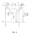
- FIG. 5 is equivalent circuitry diagram of a pixel structure according to other embodiments of the present invention.
- the embodiment is similar to the embodiment shown in FIG. 1 .
- identical components will be denoted with the same numerals and not repeated herein.
- the difference between the embodiment of FIG. 5 and the embodiment of FIG. 1 lies in that the pixel structure of FIG. 5 has only one bias line BL 2 .
- the bias line BL 2 is disposed parallel to the scan line SL.
- the second electrode E 2 of the capacitor C and the second source S 2 of the driving device T 2 are electrically connected the bias line BL 2
- the fourth gate G 4 and the fourth drain D 4 are also electrically connected to the bias line BL 2 .
- FIG. 6 is a diagram showing a top view of a pixel structure according to another embodiment of the present invention.
- the embodiment is similar to the embodiment shown in FIG. 3 .
- identical components will be denoted with the same numerals and not repeated herein.
- the difference between the embodiment of FIG. 6 and the embodiment of FIG. 3 lies in that the photo sensor device T 4 (and the second switch device T 3 ) is disposed between the first bias line BL 1 and the readout line RL.
- FIG. 7 is a cross-sectional view of a pixel structure according to another embodiment of the present invention.
- the embodiment is similar to the embodiment shown in FIG. 2 .
- identical components will be denoted with the same numerals and not repeated herein.
- the organic light emitting device O is a top emission organic light emitting device (or dual emission organic light emitting device) and the photo sensor device T 4 is a bottom gate thin film transistor.
- the upper electrode 140 of the organic light emitting device O comprises a transparent electrode material, such as Indium Tin Oxide (ITO) or Indium Zinc Oxide (IZO), and the bottom electrode 120 comprises a reflective electrode material or a transparent electrode material. If the bottom electrode 120 is a reflective electrode, the light L emitted from the organic light emitting layer 130 may pass though the upper electrode 140 , such that the organic light emitting device O is a top emission organic light emitting device. If the bottom electrode 120 is a transparent electrode, the light emitted from the organic light emitting layer 130 may pass though the upper electrode 140 and also pass through the bottom electrode 120 and the substrate 100 , such that the organic light emitting device O is a dual emission organic light emitting device.
- ITO Indium Tin Oxide
- IZO Indium Zinc Oxide
- the photo sensor device T 4 is a bottom gate thin film transistor structure. That is, the fourth gate G 4 is a part of the first conductive layer M 1 on the substrate 100 , the fourth channel CH 4 is disposed above the fourth gate G 4 , and the fourth source S 4 and the fourth drain D 4 are disposed on the fourth channel CH 4 . Since the fourth gate G 4 belongs to the first conductive layer M 1 , the bias line electrically connected to fourth gate G 4 and the fourth drain D 4 may also belong to the first conductive layer M 1 .
- the light shielding pattern can be omitted because the fourth gate G 4 is disposed under the fourth channel CH 4 to shield the light L from the organic light emitting layer 130 .
- FIGS. 8-11 are cross-sectional views of a pixel structure according to several embodiments of the present invention.
- the embodiment is similar to the embodiment shown in FIG. 2 .
- identical components will be denoted with the same numerals and not repeated herein.
- the difference between the embodiment of FIG. 8 and the embodiment of FIG. 2 lies in that the light shielding pattern B is disposed on an outer surface of the substrate 100 .
- the light shielding pattern B is disposed on the outer surface of the substrate 100 under the photo sensor device T 4 .
- the light shielding pattern B may be a color filter pattern or a black resin, for example.
- the light shielding pattern B is used to allow the specific wavelength to pass through, and enhance the sensing sensitivity of the photo sensor device T 4 .
- the embodiment is similar to the embodiment shown in FIG. 8 .
- identical components will be denoted with the same numerals and not repeated herein.
- the difference between the embodiment of FIG. 9 and the embodiment of FIG. 8 lies in that the light shielding pattern B is disposed on an inner surface of the substrate 100 .
- the light shielding pattern B is disposed between the substrate 100 and the photo sensor device T 4 .
- the light shielding pattern B may be a color filter pattern, and shield the photo sensor device T 4 from reflected light coming from the surrounding and the light L of the organic light emitting device O, to allow the specific wavelength to pass through and block the interference of the reflected light.
- the embodiment is similar to the embodiment shown in FIG. 9 .
- the organic light emitting device O comprises the touching sensing light source, such as infrared or other invisible light, except for the trichromatic light emitting diodes
- the difference between the embodiment of FIG. 10 and the embodiment of FIG. 9 lies in that the light shielding pattern B is disposed on the photo sensor device T 4 .
- the light shielding pattern B covers the gate G 4 of the photo sensor device T 4 .
- the light shielding pattern B may be a black resin, and shield the photo sensor device T 4 from reflected light L of the organic light emitting device O composed of the infrared light and the invisible light.
- the embodiment is similar to the embodiment shown in FIG. 10 .
- identical components will be denoted with the same numerals and not repeated herein.
- the difference between the embodiment of FIG. 11 and the embodiment of FIG. 10 lies in that the light shielding pattern B is disposed on the inner surface of the substrate 100 and on the photo sensor device T 4 .
- the light shielding pattern B is disposed between the substrate 100 and the photo sensor device T 4 and covers the gate G 4 of the photo sensor device T 4 .
- the light shielding pattern B may shield the photo sensor device T 4 from reflected light coming from the surrounding and the light L of the organic light emitting device O.
- FIGS. 12-13 are diagrams showing a top view of a pixel structure according to embodiments of the present invention.
- the light shielding pattern B shown in FIG. 8 , 9 , 10 or 11 is disposed corresponding to the photo sensor device T 4 , as shown in FIG. 12 and FIG. 13 .
- the light shielding pattern B mainly covers the photo sensor device T 4 and exposes other components of the pixel structure.
- the organic electroluminescence device has the touch sensing function.
- the manufacturing process of the touch sensing elements (comprising the photo sensor device, the second switch device, the readout line and the bias line) can be compliant with the manufacturing process of the organic light emitting elements (comprising the first switch device, the driving device, the organic light emitting device, the scan line and the data line), and therefore additional processes for the pixel structure are not required.
Landscapes
- Engineering & Computer Science (AREA)
- Physics & Mathematics (AREA)
- Theoretical Computer Science (AREA)
- Microelectronics & Electronic Packaging (AREA)
- General Engineering & Computer Science (AREA)
- General Physics & Mathematics (AREA)
- Optics & Photonics (AREA)
- Human Computer Interaction (AREA)
- Geometry (AREA)
- Computer Hardware Design (AREA)
- Electroluminescent Light Sources (AREA)
- Devices For Indicating Variable Information By Combining Individual Elements (AREA)
- Position Input By Displaying (AREA)
- Solid State Image Pick-Up Elements (AREA)
- Control Of Indicators Other Than Cathode Ray Tubes (AREA)
Abstract
Description
Claims (20)
Priority Applications (6)
| Application Number | Priority Date | Filing Date | Title |
|---|---|---|---|
| US13/366,270 US8902135B2 (en) | 2012-02-04 | 2012-02-04 | Pixel structure of organic electroluminescence device |
| EP13152458.9A EP2624245A3 (en) | 2012-02-04 | 2013-01-24 | Pixel structure of organic electroluminescence device |
| TW102103361A TWI512967B (en) | 2012-02-04 | 2013-01-29 | A pixel of an organic electroluminescence device |
| JP2013014808A JP5781553B2 (en) | 2012-02-04 | 2013-01-29 | Pixel structure of organic electroluminescence device |
| CN201310044046.9A CN103247664B (en) | 2012-02-04 | 2013-02-04 | The image element structure of organic electroluminescent element |
| KR1020130012512A KR101415894B1 (en) | 2012-02-04 | 2013-02-04 | Pixel structure of organic electroluminescence device |
Applications Claiming Priority (1)
| Application Number | Priority Date | Filing Date | Title |
|---|---|---|---|
| US13/366,270 US8902135B2 (en) | 2012-02-04 | 2012-02-04 | Pixel structure of organic electroluminescence device |
Publications (2)
| Publication Number | Publication Date |
|---|---|
| US20130201085A1 US20130201085A1 (en) | 2013-08-08 |
| US8902135B2 true US8902135B2 (en) | 2014-12-02 |
Family
ID=47623938
Family Applications (1)
| Application Number | Title | Priority Date | Filing Date |
|---|---|---|---|
| US13/366,270 Active 2033-03-24 US8902135B2 (en) | 2012-02-04 | 2012-02-04 | Pixel structure of organic electroluminescence device |
Country Status (6)
| Country | Link |
|---|---|
| US (1) | US8902135B2 (en) |
| EP (1) | EP2624245A3 (en) |
| JP (1) | JP5781553B2 (en) |
| KR (1) | KR101415894B1 (en) |
| CN (1) | CN103247664B (en) |
| TW (1) | TWI512967B (en) |
Cited By (1)
| Publication number | Priority date | Publication date | Assignee | Title |
|---|---|---|---|---|
| US9331107B2 (en) | 2013-11-06 | 2016-05-03 | Au Optronics Corporation | Pixel structure |
Families Citing this family (18)
| Publication number | Priority date | Publication date | Assignee | Title |
|---|---|---|---|---|
| KR101991338B1 (en) * | 2012-09-24 | 2019-06-20 | 엘지디스플레이 주식회사 | Thin film transistor array substrate and method for manufacturing of the same |
| CN103413522B (en) * | 2013-07-31 | 2015-04-22 | 京东方科技集团股份有限公司 | Pixel circuit, organic electroluminescence display panel and display device |
| TWI511283B (en) * | 2013-11-07 | 2015-12-01 | Chunghwa Picture Tubes Ltd | Pixel array substrate and organic light-emitting diode display |
| KR20160145643A (en) * | 2014-04-23 | 2016-12-20 | 가부시키가이샤 한도오따이 에네루기 켄큐쇼 | Input/output device and method for driving input/output device |
| CN105468205B (en) * | 2014-09-03 | 2018-08-31 | 上海和辉光电有限公司 | The touch device and preparation method thereof being integrated in AMOLED panel |
| KR102172389B1 (en) * | 2014-12-30 | 2020-10-30 | 엘지디스플레이 주식회사 | Organic light emitting display |
| TWI580015B (en) * | 2015-08-24 | 2017-04-21 | 友達光電股份有限公司 | Pixel array |
| KR102430575B1 (en) * | 2015-08-26 | 2022-08-08 | 엘지디스플레이 주식회사 | Organic Light Emitting Display Device and Method for the Same |
| JP6698486B2 (en) * | 2016-09-26 | 2020-05-27 | 株式会社ジャパンディスプレイ | Display device |
| KR102555180B1 (en) * | 2016-11-30 | 2023-07-13 | 엘지디스플레이 주식회사 | Touch display device, display panel, and all in one switch device |
| CN106708326A (en) * | 2017-01-10 | 2017-05-24 | 京东方科技集团股份有限公司 | Touch substrate and display device |
| CN106940602B (en) * | 2017-03-14 | 2020-04-03 | 合肥鑫晟光电科技有限公司 | Display panel, photosensitive touch circuit and control method thereof |
| CN109509767B (en) * | 2017-09-15 | 2024-07-12 | 京东方科技集团股份有限公司 | Display panel and display device |
| US20200111815A1 (en) * | 2018-10-09 | 2020-04-09 | Innolux Corporation | Display device |
| TWI724846B (en) * | 2020-03-30 | 2021-04-11 | 友達光電股份有限公司 | Sensing device and sensing method |
| CN113497160B (en) * | 2020-04-08 | 2024-04-23 | 和鑫光电股份有限公司 | Light sensing device, light sensing panel and light sensing display panel using same |
| JP7065147B2 (en) * | 2020-04-28 | 2022-05-11 | 株式会社ジャパンディスプレイ | Semiconductor device |
| US11830904B2 (en) * | 2020-07-08 | 2023-11-28 | Hannstouch Solution Incorporated | Light sensing device having offset gate electrode and light sensing panel and light sensing display panel using the same |
Citations (7)
| Publication number | Priority date | Publication date | Assignee | Title |
|---|---|---|---|---|
| US20020000576A1 (en) * | 2000-06-22 | 2002-01-03 | Kazutaka Inukai | Display device |
| US20070152180A1 (en) * | 2006-01-04 | 2007-07-05 | Toppoly Optoelectronics Corp. | Organic electroluminescent devices and fabrication methods thereof |
| JP2009244638A (en) | 2008-03-31 | 2009-10-22 | Mitsubishi Electric Corp | Display device including optical sensor |
| JP2009283676A (en) | 2008-05-22 | 2009-12-03 | Toshiba Mobile Display Co Ltd | Organic el display apparatus |
| US7915617B2 (en) * | 2005-07-04 | 2011-03-29 | Kabushiki Kaisha Toshiba | Semiconductor device |
| JP2011102960A (en) | 2009-11-10 | 2011-05-26 | Samsung Mobile Display Co Ltd | Organic light emitting diode display and method for manufacturing the same |
| US20120313913A1 (en) * | 2010-02-26 | 2012-12-13 | Sharp Kabushiki Kaisha | Display device |
Family Cites Families (6)
| Publication number | Priority date | Publication date | Assignee | Title |
|---|---|---|---|---|
| JPH1090655A (en) * | 1996-09-17 | 1998-04-10 | Toshiba Corp | Display device |
| JP3959454B2 (en) * | 2001-10-22 | 2007-08-15 | シャープ株式会社 | Input device and input / output device |
| JP2006267967A (en) * | 2005-03-25 | 2006-10-05 | Toshiba Matsushita Display Technology Co Ltd | Flat-panel display device |
| TWI253846B (en) * | 2005-03-28 | 2006-04-21 | Ind Tech Res Inst | Photo-sensing display unit |
| US8203645B2 (en) * | 2007-08-10 | 2012-06-19 | Canon Kabushiki Kaisha | Image-pickup apparatus and control method thereof with image generation based on a detected spatial frequency |
| TWI399680B (en) * | 2009-05-11 | 2013-06-21 | Innolux Corp | Touch display panel, touch display apparatus and control methods thereof |
-
2012
- 2012-02-04 US US13/366,270 patent/US8902135B2/en active Active
-
2013
- 2013-01-24 EP EP13152458.9A patent/EP2624245A3/en not_active Ceased
- 2013-01-29 TW TW102103361A patent/TWI512967B/en active
- 2013-01-29 JP JP2013014808A patent/JP5781553B2/en not_active Expired - Fee Related
- 2013-02-04 KR KR1020130012512A patent/KR101415894B1/en active IP Right Grant
- 2013-02-04 CN CN201310044046.9A patent/CN103247664B/en active Active
Patent Citations (7)
| Publication number | Priority date | Publication date | Assignee | Title |
|---|---|---|---|---|
| US20020000576A1 (en) * | 2000-06-22 | 2002-01-03 | Kazutaka Inukai | Display device |
| US7915617B2 (en) * | 2005-07-04 | 2011-03-29 | Kabushiki Kaisha Toshiba | Semiconductor device |
| US20070152180A1 (en) * | 2006-01-04 | 2007-07-05 | Toppoly Optoelectronics Corp. | Organic electroluminescent devices and fabrication methods thereof |
| JP2009244638A (en) | 2008-03-31 | 2009-10-22 | Mitsubishi Electric Corp | Display device including optical sensor |
| JP2009283676A (en) | 2008-05-22 | 2009-12-03 | Toshiba Mobile Display Co Ltd | Organic el display apparatus |
| JP2011102960A (en) | 2009-11-10 | 2011-05-26 | Samsung Mobile Display Co Ltd | Organic light emitting diode display and method for manufacturing the same |
| US20120313913A1 (en) * | 2010-02-26 | 2012-12-13 | Sharp Kabushiki Kaisha | Display device |
Non-Patent Citations (2)
| Title |
|---|
| "Office Action of Japan Counterpart Application", issued on Jan. 7, 2014, p .1-p. 3, in which the listed references(Ref. 1-3) were cited. |
| "Office Action of Korean Counterpart Application", issued on Mar. 4, 2014, with English translation thereof, p. 1-p. 7, in which the listed reference(Ref. 1) was cited. |
Cited By (2)
| Publication number | Priority date | Publication date | Assignee | Title |
|---|---|---|---|---|
| US9331107B2 (en) | 2013-11-06 | 2016-05-03 | Au Optronics Corporation | Pixel structure |
| US9331106B2 (en) | 2013-11-06 | 2016-05-03 | Au Optronics Corporation | Pixel structure and fabrication method thereof |
Also Published As
| Publication number | Publication date |
|---|---|
| KR101415894B1 (en) | 2014-07-04 |
| JP5781553B2 (en) | 2015-09-24 |
| EP2624245A3 (en) | 2016-11-09 |
| CN103247664B (en) | 2016-11-23 |
| TWI512967B (en) | 2015-12-11 |
| KR20130090825A (en) | 2013-08-14 |
| EP2624245A2 (en) | 2013-08-07 |
| TW201334178A (en) | 2013-08-16 |
| US20130201085A1 (en) | 2013-08-08 |
| CN103247664A (en) | 2013-08-14 |
| JP2013174877A (en) | 2013-09-05 |
Similar Documents
| Publication | Publication Date | Title |
|---|---|---|
| US8902135B2 (en) | Pixel structure of organic electroluminescence device | |
| US11003006B2 (en) | Touch input device | |
| CN107346192B (en) | Electronic device and display module provided therein | |
| KR102269919B1 (en) | Display device comprising touch sensor | |
| US8537149B2 (en) | Pixel array and display panel having the same | |
| US8901549B2 (en) | Organic light emitting diode touch display panel | |
| US20170269751A1 (en) | Touch input device | |
| CN106354296B (en) | Display device | |
| KR20210018720A (en) | Display device | |
| CN113140600A (en) | Display device | |
| US20190155438A1 (en) | Touch input device | |
| US20230118413A1 (en) | Display device | |
| CN219108131U (en) | Display device | |
| KR102627915B1 (en) | Touch sensible organic light emitting diode display | |
| US20240107851A1 (en) | Display device and method of manufacturing the same | |
| KR20240055919A (en) | Display device | |
| US20230083612A1 (en) | Display device | |
| KR20230144679A (en) | Display device | |
| CN116895082A (en) | Display device and driving method thereof | |
| CN116896954A (en) | display device | |
| KR20170013146A (en) | Smartphone |
Legal Events
| Date | Code | Title | Description |
|---|---|---|---|
| AS | Assignment |
Owner name: INTEGRATED DIGITAL TECHNOLOGIES, INC., TAIWAN Free format text: ASSIGNMENT OF ASSIGNORS INTEREST;ASSIGNORS:CHANG, YANG-HUI;HWANG, NAE-JYE;LIAW, SHEN-TAI;REEL/FRAME:027660/0618 Effective date: 20120204 |
|
| STCF | Information on status: patent grant |
Free format text: PATENTED CASE |
|
| AS | Assignment |
Owner name: SHANGHAI XUANYAN ELECTRONIC TECHNOLOGIES, INC, CHI Free format text: ASSIGNMENT OF ASSIGNORS INTEREST;ASSIGNOR:INTEGRATED DIGITAL TECHNOLOGIES, INC.;REEL/FRAME:039598/0623 Effective date: 20160816 |
|
| FEPP | Fee payment procedure |
Free format text: SURCHARGE FOR LATE PAYMENT, SMALL ENTITY (ORIGINAL EVENT CODE: M2554) |
|
| MAFP | Maintenance fee payment |
Free format text: PAYMENT OF MAINTENANCE FEE, 4TH YR, SMALL ENTITY (ORIGINAL EVENT CODE: M2551) Year of fee payment: 4 |
|
| AS | Assignment |
Owner name: HELLOSI INTEGRATED CIRCUIT INC., CHINA Free format text: ASSIGNMENT OF ASSIGNORS INTEREST;ASSIGNOR:SHANGHAI XUANYAN ELECTRONIC TECHNOLOGIES, INC.;REEL/FRAME:058265/0190 Effective date: 20211130 |
|
| MAFP | Maintenance fee payment |
Free format text: PAYMENT OF MAINTENANCE FEE, 8TH YR, SMALL ENTITY (ORIGINAL EVENT CODE: M2552); ENTITY STATUS OF PATENT OWNER: SMALL ENTITY Year of fee payment: 8 |