US8884379B2 - Strain engineering in semiconductor devices by using a piezoelectric material - Google Patents
Strain engineering in semiconductor devices by using a piezoelectric material Download PDFInfo
- Publication number
- US8884379B2 US8884379B2 US12/711,322 US71132210A US8884379B2 US 8884379 B2 US8884379 B2 US 8884379B2 US 71132210 A US71132210 A US 71132210A US 8884379 B2 US8884379 B2 US 8884379B2
- Authority
- US
- United States
- Prior art keywords
- region
- piezoelectric
- strain
- active
- active region
- Prior art date
- Legal status (The legal status is an assumption and is not a legal conclusion. Google has not performed a legal analysis and makes no representation as to the accuracy of the status listed.)
- Expired - Fee Related, expires
Links
- 239000000463 material Substances 0.000 title claims abstract description 128
- 239000004065 semiconductor Substances 0.000 title claims description 113
- 230000001939 inductive effect Effects 0.000 claims abstract description 31
- 238000000034 method Methods 0.000 claims description 77
- 239000000758 substrate Substances 0.000 claims description 51
- 230000005684 electric field Effects 0.000 claims description 42
- 238000002955 isolation Methods 0.000 claims description 13
- 230000005669 field effect Effects 0.000 claims description 11
- 238000009413 insulation Methods 0.000 claims description 6
- 230000003213 activating effect Effects 0.000 claims 2
- 230000007246 mechanism Effects 0.000 abstract description 16
- 238000004519 manufacturing process Methods 0.000 description 24
- 230000008569 process Effects 0.000 description 22
- 230000035882 stress Effects 0.000 description 19
- XUIMIQQOPSSXEZ-UHFFFAOYSA-N Silicon Chemical compound [Si] XUIMIQQOPSSXEZ-UHFFFAOYSA-N 0.000 description 17
- 239000011810 insulating material Substances 0.000 description 17
- 239000010703 silicon Substances 0.000 description 17
- 229910052710 silicon Inorganic materials 0.000 description 14
- 239000012876 carrier material Substances 0.000 description 13
- FVBUAEGBCNSCDD-UHFFFAOYSA-N silicide(4-) Chemical compound [Si-4] FVBUAEGBCNSCDD-UHFFFAOYSA-N 0.000 description 13
- VYPSYNLAJGMNEJ-UHFFFAOYSA-N silicon dioxide Inorganic materials O=[Si]=O VYPSYNLAJGMNEJ-UHFFFAOYSA-N 0.000 description 11
- 230000001965 increasing effect Effects 0.000 description 10
- 239000003989 dielectric material Substances 0.000 description 9
- 238000013459 approach Methods 0.000 description 7
- 238000005516 engineering process Methods 0.000 description 7
- 238000002513 implantation Methods 0.000 description 7
- 230000008901 benefit Effects 0.000 description 6
- 230000002708 enhancing effect Effects 0.000 description 6
- 230000009467 reduction Effects 0.000 description 6
- 235000012239 silicon dioxide Nutrition 0.000 description 6
- 229910045601 alloy Inorganic materials 0.000 description 5
- 239000000956 alloy Substances 0.000 description 5
- 238000000151 deposition Methods 0.000 description 5
- 230000000694 effects Effects 0.000 description 5
- 239000000377 silicon dioxide Substances 0.000 description 5
- 230000006978 adaptation Effects 0.000 description 4
- 239000002800 charge carrier Substances 0.000 description 4
- 238000011161 development Methods 0.000 description 4
- 230000018109 developmental process Effects 0.000 description 4
- 239000002019 doping agent Substances 0.000 description 4
- 229910052732 germanium Inorganic materials 0.000 description 4
- GNPVGFCGXDBREM-UHFFFAOYSA-N germanium atom Chemical compound [Ge] GNPVGFCGXDBREM-UHFFFAOYSA-N 0.000 description 4
- 238000001459 lithography Methods 0.000 description 4
- 238000012545 processing Methods 0.000 description 4
- 125000006850 spacer group Chemical group 0.000 description 4
- 229910000676 Si alloy Inorganic materials 0.000 description 3
- 230000008602 contraction Effects 0.000 description 3
- 239000002178 crystalline material Substances 0.000 description 3
- 230000008021 deposition Effects 0.000 description 3
- 238000013461 design Methods 0.000 description 3
- 229910052751 metal Inorganic materials 0.000 description 3
- 239000002184 metal Substances 0.000 description 3
- 230000004048 modification Effects 0.000 description 3
- 238000012986 modification Methods 0.000 description 3
- 239000002210 silicon-based material Substances 0.000 description 3
- 230000003068 static effect Effects 0.000 description 3
- 235000012431 wafers Nutrition 0.000 description 3
- 229910000927 Ge alloy Inorganic materials 0.000 description 2
- 229910052581 Si3N4 Inorganic materials 0.000 description 2
- 229910010293 ceramic material Inorganic materials 0.000 description 2
- 230000008878 coupling Effects 0.000 description 2
- 238000010168 coupling process Methods 0.000 description 2
- 238000005859 coupling reaction Methods 0.000 description 2
- 239000013078 crystal Substances 0.000 description 2
- 239000007772 electrode material Substances 0.000 description 2
- 238000005530 etching Methods 0.000 description 2
- 230000006355 external stress Effects 0.000 description 2
- 229910021332 silicide Inorganic materials 0.000 description 2
- HQVNEWCFYHHQES-UHFFFAOYSA-N silicon nitride Chemical compound N12[Si]34N5[Si]62N3[Si]51N64 HQVNEWCFYHHQES-UHFFFAOYSA-N 0.000 description 2
- 238000012546 transfer Methods 0.000 description 2
- 229910001339 C alloy Inorganic materials 0.000 description 1
- 230000032683 aging Effects 0.000 description 1
- 230000004075 alteration Effects 0.000 description 1
- 229910052782 aluminium Inorganic materials 0.000 description 1
- XAGFODPZIPBFFR-UHFFFAOYSA-N aluminium Chemical compound [Al] XAGFODPZIPBFFR-UHFFFAOYSA-N 0.000 description 1
- 230000015572 biosynthetic process Effects 0.000 description 1
- 239000003990 capacitor Substances 0.000 description 1
- 239000011365 complex material Substances 0.000 description 1
- 239000002131 composite material Substances 0.000 description 1
- 238000010276 construction Methods 0.000 description 1
- 230000003247 decreasing effect Effects 0.000 description 1
- 238000001514 detection method Methods 0.000 description 1
- 238000006073 displacement reaction Methods 0.000 description 1
- 238000010292 electrical insulation Methods 0.000 description 1
- 230000006872 improvement Effects 0.000 description 1
- 239000012212 insulator Substances 0.000 description 1
- 230000002452 interceptive effect Effects 0.000 description 1
- GQYHUHYESMUTHG-UHFFFAOYSA-N lithium niobate Chemical compound [Li+].[O-][Nb](=O)=O GQYHUHYESMUTHG-UHFFFAOYSA-N 0.000 description 1
- 239000000203 mixture Substances 0.000 description 1
- 238000012856 packing Methods 0.000 description 1
- 230000003071 parasitic effect Effects 0.000 description 1
- 238000000059 patterning Methods 0.000 description 1
- 238000005498 polishing Methods 0.000 description 1
- LJCNRYVRMXRIQR-OLXYHTOASA-L potassium sodium L-tartrate Chemical compound [Na+].[K+].[O-]C(=O)[C@H](O)[C@@H](O)C([O-])=O LJCNRYVRMXRIQR-OLXYHTOASA-L 0.000 description 1
- 239000010453 quartz Substances 0.000 description 1
- 238000001953 recrystallisation Methods 0.000 description 1
- 238000005549 size reduction Methods 0.000 description 1
- 235000011006 sodium potassium tartrate Nutrition 0.000 description 1
- 238000003860 storage Methods 0.000 description 1
- 238000004381 surface treatment Methods 0.000 description 1
- 239000011032 tourmaline Substances 0.000 description 1
- 229940070527 tourmaline Drugs 0.000 description 1
- 229910052613 tourmaline Inorganic materials 0.000 description 1
- 230000007704 transition Effects 0.000 description 1
- WFKWXMTUELFFGS-UHFFFAOYSA-N tungsten Chemical compound [W] WFKWXMTUELFFGS-UHFFFAOYSA-N 0.000 description 1
- 239000010937 tungsten Substances 0.000 description 1
- 229910052721 tungsten Inorganic materials 0.000 description 1
Images


Classifications
-
- H—ELECTRICITY
- H01—ELECTRIC ELEMENTS
- H01L—SEMICONDUCTOR DEVICES NOT COVERED BY CLASS H10
- H01L27/00—Devices consisting of a plurality of semiconductor or other solid-state components formed in or on a common substrate
- H01L27/02—Devices consisting of a plurality of semiconductor or other solid-state components formed in or on a common substrate including semiconductor components specially adapted for rectifying, oscillating, amplifying or switching and having at least one potential-jump barrier or surface barrier; including integrated passive circuit elements with at least one potential-jump barrier or surface barrier
- H01L27/12—Devices consisting of a plurality of semiconductor or other solid-state components formed in or on a common substrate including semiconductor components specially adapted for rectifying, oscillating, amplifying or switching and having at least one potential-jump barrier or surface barrier; including integrated passive circuit elements with at least one potential-jump barrier or surface barrier the substrate being other than a semiconductor body, e.g. an insulating body
- H01L27/1203—Devices consisting of a plurality of semiconductor or other solid-state components formed in or on a common substrate including semiconductor components specially adapted for rectifying, oscillating, amplifying or switching and having at least one potential-jump barrier or surface barrier; including integrated passive circuit elements with at least one potential-jump barrier or surface barrier the substrate being other than a semiconductor body, e.g. an insulating body the substrate comprising an insulating body on a semiconductor body, e.g. SOI
-
- H01L27/20—
-
- H—ELECTRICITY
- H01—ELECTRIC ELEMENTS
- H01L—SEMICONDUCTOR DEVICES NOT COVERED BY CLASS H10
- H01L29/00—Semiconductor devices adapted for rectifying, amplifying, oscillating or switching, or capacitors or resistors with at least one potential-jump barrier or surface barrier, e.g. PN junction depletion layer or carrier concentration layer; Details of semiconductor bodies or of electrodes thereof ; Multistep manufacturing processes therefor
- H01L29/66—Types of semiconductor device ; Multistep manufacturing processes therefor
- H01L29/68—Types of semiconductor device ; Multistep manufacturing processes therefor controllable by only the electric current supplied, or only the electric potential applied, to an electrode which does not carry the current to be rectified, amplified or switched
- H01L29/76—Unipolar devices, e.g. field effect transistors
- H01L29/772—Field effect transistors
- H01L29/78—Field effect transistors with field effect produced by an insulated gate
- H01L29/7842—Field effect transistors with field effect produced by an insulated gate means for exerting mechanical stress on the crystal lattice of the channel region, e.g. using a flexible substrate
- H01L29/7843—Field effect transistors with field effect produced by an insulated gate means for exerting mechanical stress on the crystal lattice of the channel region, e.g. using a flexible substrate the means being an applied insulating layer
-
- H—ELECTRICITY
- H01—ELECTRIC ELEMENTS
- H01L—SEMICONDUCTOR DEVICES NOT COVERED BY CLASS H10
- H01L29/00—Semiconductor devices adapted for rectifying, amplifying, oscillating or switching, or capacitors or resistors with at least one potential-jump barrier or surface barrier, e.g. PN junction depletion layer or carrier concentration layer; Details of semiconductor bodies or of electrodes thereof ; Multistep manufacturing processes therefor
- H01L29/66—Types of semiconductor device ; Multistep manufacturing processes therefor
- H01L29/68—Types of semiconductor device ; Multistep manufacturing processes therefor controllable by only the electric current supplied, or only the electric potential applied, to an electrode which does not carry the current to be rectified, amplified or switched
- H01L29/76—Unipolar devices, e.g. field effect transistors
- H01L29/772—Field effect transistors
- H01L29/78—Field effect transistors with field effect produced by an insulated gate
- H01L29/7842—Field effect transistors with field effect produced by an insulated gate means for exerting mechanical stress on the crystal lattice of the channel region, e.g. using a flexible substrate
- H01L29/7849—Field effect transistors with field effect produced by an insulated gate means for exerting mechanical stress on the crystal lattice of the channel region, e.g. using a flexible substrate the means being provided under the channel
-
- H—ELECTRICITY
- H10—SEMICONDUCTOR DEVICES; ELECTRIC SOLID-STATE DEVICES NOT OTHERWISE PROVIDED FOR
- H10N—ELECTRIC SOLID-STATE DEVICES NOT OTHERWISE PROVIDED FOR
- H10N39/00—Integrated devices, or assemblies of multiple devices, comprising at least one piezoelectric, electrostrictive or magnetostrictive element covered by groups H10N30/00 – H10N35/00
-
- H—ELECTRICITY
- H01—ELECTRIC ELEMENTS
- H01L—SEMICONDUCTOR DEVICES NOT COVERED BY CLASS H10
- H01L21/00—Processes or apparatus adapted for the manufacture or treatment of semiconductor or solid state devices or of parts thereof
- H01L21/70—Manufacture or treatment of devices consisting of a plurality of solid state components formed in or on a common substrate or of parts thereof; Manufacture of integrated circuit devices or of parts thereof
- H01L21/77—Manufacture or treatment of devices consisting of a plurality of solid state components or integrated circuits formed in, or on, a common substrate
- H01L21/78—Manufacture or treatment of devices consisting of a plurality of solid state components or integrated circuits formed in, or on, a common substrate with subsequent division of the substrate into plural individual devices
- H01L21/82—Manufacture or treatment of devices consisting of a plurality of solid state components or integrated circuits formed in, or on, a common substrate with subsequent division of the substrate into plural individual devices to produce devices, e.g. integrated circuits, each consisting of a plurality of components
- H01L21/822—Manufacture or treatment of devices consisting of a plurality of solid state components or integrated circuits formed in, or on, a common substrate with subsequent division of the substrate into plural individual devices to produce devices, e.g. integrated circuits, each consisting of a plurality of components the substrate being a semiconductor, using silicon technology
- H01L21/8232—Field-effect technology
- H01L21/8234—MIS technology, i.e. integration processes of field effect transistors of the conductor-insulator-semiconductor type
- H01L21/823412—MIS technology, i.e. integration processes of field effect transistors of the conductor-insulator-semiconductor type with a particular manufacturing method of the channel structures, e.g. channel implants, halo or pocket implants, or channel materials
-
- H—ELECTRICITY
- H01—ELECTRIC ELEMENTS
- H01L—SEMICONDUCTOR DEVICES NOT COVERED BY CLASS H10
- H01L21/00—Processes or apparatus adapted for the manufacture or treatment of semiconductor or solid state devices or of parts thereof
- H01L21/70—Manufacture or treatment of devices consisting of a plurality of solid state components formed in or on a common substrate or of parts thereof; Manufacture of integrated circuit devices or of parts thereof
- H01L21/77—Manufacture or treatment of devices consisting of a plurality of solid state components or integrated circuits formed in, or on, a common substrate
- H01L21/78—Manufacture or treatment of devices consisting of a plurality of solid state components or integrated circuits formed in, or on, a common substrate with subsequent division of the substrate into plural individual devices
- H01L21/82—Manufacture or treatment of devices consisting of a plurality of solid state components or integrated circuits formed in, or on, a common substrate with subsequent division of the substrate into plural individual devices to produce devices, e.g. integrated circuits, each consisting of a plurality of components
- H01L21/822—Manufacture or treatment of devices consisting of a plurality of solid state components or integrated circuits formed in, or on, a common substrate with subsequent division of the substrate into plural individual devices to produce devices, e.g. integrated circuits, each consisting of a plurality of components the substrate being a semiconductor, using silicon technology
- H01L21/8232—Field-effect technology
- H01L21/8234—MIS technology, i.e. integration processes of field effect transistors of the conductor-insulator-semiconductor type
- H01L21/8238—Complementary field-effect transistors, e.g. CMOS
- H01L21/823807—Complementary field-effect transistors, e.g. CMOS with a particular manufacturing method of the channel structures, e.g. channel implants, halo or pocket implants, or channel materials
Definitions
- the present disclosure relates to the field of integrated circuits, and, more particularly, to the manufacture of circuit elements, such as transistors, having strained semiconductor regions, such as channel regions, by using stress-inducing sources, such as globally strained silicon substrates and the like, to enhance charge carrier mobility in the strained semiconductor regions.
- CMOS technology is presently one of the most promising approaches due to the superior characteristics in view of operating speed and/or power consumption and/or cost efficiency.
- millions of transistors i.e., N-channel transistors and P-channel transistors, are formed on a substrate including a crystalline semiconductor layer.
- a MOS transistor irrespective of whether an N-channel transistor or a P-channel transistor is considered, comprises so-called PN junctions that are formed by an interface of highly doped drain and source regions with an inversely or weakly doped channel region disposed between the drain region and the source region.
- the conductivity of the channel region i.e., the drive current capability of the conductive channel, is controlled by a gate electrode located close to the channel region and separated therefrom by a thin insulating layer.
- the conductivity of the channel region upon formation of a conductive channel due to the application of an appropriate control voltage to the gate electrode, depends on the dopant concentration, the mobility of the charge carriers and, for a given extension of the channel region in the transistor width direction, on the distance between the source and drain regions, which is also referred to as channel length.
- the conductivity of the channel region is a dominant factor determining the performance of MOS transistors.
- the reduction of the channel length, and associated therewith the reduction of the channel resistivity is an important design criterion for accomplishing an increase in the operating speed of the integrated circuits.
- the continuing shrinkage of the transistor dimensions involves a plurality of issues associated therewith, such as reduced controllability of the channel, also referred to as short channel effects, and the like, that have to be addressed so as to not unduly offset the advantages obtained by steadily decreasing the channel length of MOS transistors.
- the thickness of the gate insulation layer typically an oxide-based dielectric
- the thickness of the gate insulation layer has to be reduced with reducing the gate length, wherein a reduced thickness of the gate dielectric may result in increased leakage currents, thereby posing limitations for oxide-based gate insulation layers at approximately 1-2 nm.
- the continuous size reduction of the critical dimensions necessitates the adaptation and possibly the new development of highly complex process techniques, for example, for compensating for short channel effects with oxide-based gate dielectric scaling being pushed to the limits with respect to tolerable leakage currents.
- One efficient mechanism for increasing the charge carrier mobility is the modification of the lattice structure in the channel region, for instance by creating tensile or compressive stress in the vicinity of the channel region so as to produce a corresponding strain in the channel region, which results in a modified mobility for electrons and holes, respectively.
- creating uniaxial tensile strain in the channel region along the channel length direction for a standard crystallographic orientation increases the mobility of electrons, which in turn may directly translate into a corresponding increase in the conductivity.
- uniaxial compressive strain in the channel region for the same configuration as above may increase the mobility of holes, thereby providing the potential for enhancing the performance of P-type transistors.
- strained silicon may be considered as a “new” type of semiconductor material, which may enable the fabrication of fast powerful semiconductor devices without requiring expensive semiconductor materials, while many of the well-established manufacturing techniques may still be used.
- a stress component created by, for instance, permanent overlaying layers, spacer elements and the like is used in an attempt to create a desired strain within the channel region.
- the process of creating the strain in the channel region by applying a specified external stress may depend on the efficiency of the stress transfer mechanism for the external stress provided, for instance, by contact layers, spacers and the like into the channel region to create the desired strain therein.
- differently stressed overlayers have to be provided, which may result in a plurality of additional process steps, wherein, in particular, any additional lithography steps may contribute significantly to the overall production costs.
- the amount of stress-inducing material and in particular the intrinsic stress thereof may not be arbitrarily increased without requiring significant design alterations.
- the degree of tensile stress in corresponding portions of the dielectric layer formed above an N-channel transistor may presently be limited to approximately 1.5 GPa (Giga Pascale), while the amount of tensile stressed material may have to be reduced in sophisticated transistor geometries including reduced distances of neighboring transistor elements in device areas of high packing density, and thus new developments of respective deposition techniques may be required for further improving performance of N-channel transistors on the basis of stressed overlayers.
- significantly higher compressive stress levels may be provided for P-channel transistors by presently established techniques, thereby creating an imbalance with respect to enhancing performance of NMOS and PMOS transistors.
- a substantially amorphized region may be formed adjacent to the gate electrode at an intermediate manufacturing stage, which may then be re-crystallized in the presence of a rigid layer formed above the transistor area.
- the growth of the crystal will occur under stress conditions created by the overlayer and result in a tensile strained crystal.
- the sacrificial stress layer may be removed, wherein, nevertheless, a certain amount of strain may be “conserved” in the re-grown lattice portion. This effect is generally known as stress memorization.
- a strain-inducing semiconductor alloy may be provided within drain and source regions, which may exert a specified type of stress on the channel region to thereby induce a desired type of strain therein.
- a silicon/germanium alloy may frequently be used for this purpose in order to obtain a compressive stress component in the adjacent channel region of, for instance, P-channel transistors in order to increase mobility of holes in the corresponding P-channel.
- two or more of the above-specified strain-inducing mechanisms may be combined to further enhance the overall strain obtained in the corresponding channel regions.
- strain-inducing mechanisms may be considered as “local” mechanisms, since the strain may be induced in and above the corresponding active region for the transistor element under consideration, wherein the finally obtained strain component in the channel region may significantly depend on the overall device dimensions. That is, typically, these local strain-inducing mechanisms may rely on the stress transfer capabilities via other device components, such as gate electrodes, spacer elements formed on sidewalls of the gate electrodes, the lateral dimensions of the drain and source regions and the like. Consequently, the magnitude of the strain in the channel region may significantly depend on the technology under consideration, since, typically, reduced device dimensions may result in an over-proportional reduction of the corresponding strain-inducing mechanism.
- creating strain by a dielectric overlayer such as a contact etch stop layer
- a dielectric overlayer such as a contact etch stop layer
- the amount of internal stress of the corresponding dielectric material may be restricted by deposition-related constraints, while at the same time, upon reducing device dimensions, for instance the spacing between two neighboring transistor elements, may require a significant reduction of the layer thickness, which may thus result in a reduction of the finally obtained strain component.
- the magnitude of the strain in the channel region provided by the local strain-inducing mechanisms may be several hundred MPa, while a further increase of this value may be difficult to be achieved upon further device scaling.
- a moderately high degree of strain may be created in a global manner, i.e., on wafer level, so that the corresponding active regions of the transistor elements may be formed in a globally strained semiconductor material, thereby providing a “direct” strain component in the corresponding channel regions.
- a silicon material may be epitaxially grown on an appropriately designed “buffer layer” in order to obtain a strained silicon layer.
- a silicon/germanium buffer layer which may be provided with its substantially natural lattice constant, may be used for forming thereon a strained silicon layer, which may have a moderately high tensile biaxial strain of 1 GPa or higher, depending on the lattice mismatch between the buffer layer and the strained silicon layer.
- the approach of applying a global strain-inducing layer across the entire substrate may enable a highly efficient strain-inducing mechanism for one type of transistor while possibly negatively affecting performance of the other type of transistor. Consequently, when combining the advantages of a global strain-inducing material with strain engineering techniques allowing a local adaptation of the strain conditions in a certain type of transistor, a significant degree of process complexity may also be involved since, for instance, the strain-inducing effect of the global strain layer may have to be locally relaxed or over-compensated for by specifically designed local strain techniques.
- the present disclosure is directed to various methods that may avoid, or at least reduce, the effects of one or more of the problems identified above.
- the present disclosure relates to techniques and devices for enhancing strain engineering techniques during the fabrication of sophisticated semiconductor devices by using a piezoelectric material that may be mechanically coupled to a semiconductor region of interest so as to induce a desired type of strain therein.
- Piezoelectric materials are typically crystalline materials or ceramic materials having a very low conductivity and may thus be considered as insulating materials.
- a substantial mechanical displacement i.e., a contraction or expansion, may be induced, which may, therefore, be efficiently used as a strain-inducing mechanism by transferring the strain into the mechanically coupled semiconductor region.
- the piezoelectric material may be provided in a global manner, for instance in the form of an appropriately prepared substrate material for the fabrication of semiconductor devices, wherein a local adaptation of the strain characteristics may be efficiently achieved on the basis of providing an appropriate contact regime for establishing a desired electric field in a highly local manner.
- the active regions of individual transistor elements receive an appropriate contact regime so as to allow individual adjustment of the magnitude and/or type of strain induced by the piezoelectric material, while, on the other hand, device areas may receive strain conditions on a more global scale, for instance by commonly controlling the strain conditions for a plurality of active regions or generally for a plurality of circuit elements, if appropriate.
- One illustrative semiconductor device disclosed herein comprises a semiconductor region formed above a substrate. Furthermore, a contact structure connects to the semiconductor region to define the direction of current flow through the semiconductor region. Additionally, the semiconductor device comprises a piezoelectric region formed above the substrate so as to be mechanically coupled to the semiconductor region. A first contact is provided and connects to a first contact portion of the piezoelectric region. Furthermore, a second contact is provided to connect to a second contact portion of the piezoelectric region, wherein the first and second contact portions of the piezoelectric region are positioned so as to define an electric field direction in the piezoelectric region that is aligned to the direction of current flow through the semiconductor region.
- One illustrative substrate for forming semiconductor devices disclosed herein comprises a carrier material and a buried insulating material formed on the carrier material, wherein the buried insulating material comprises a piezoelectric material layer. Moreover, the substrate comprises a crystalline semiconductor layer formed on the buried insulating material.
- One illustrative method disclosed herein relates to generating strain in a semiconductor device.
- the method comprises providing a piezoelectric region so as to be mechanically coupled to an active region of a semiconductor circuit element.
- the method further comprises generating an electric field in the piezoelectric region so as to be aligned with a current flow direction in the active region, wherein the electric field induces one of a compressive strain and a tensile strain in the active region along the current flow direction. Finally, a current flow is established in the active region.
- FIGS. 1 a - 1 c schematically illustrate cross-sectional views of a substrate for forming semiconductor devices, wherein the substrate comprises a buried insulating material including a piezoelectric material, according to various illustrative embodiments;
- FIG. 1 d schematically illustrates a top view of a substrate including a piezoelectric material having an orientation that is aligned with respect to a current flow direction of circuit elements to be formed on the basis of the substrate, according to illustrative embodiments;
- FIG. 2 a schematically illustrates a top view of a semiconductor device in which one or more circuit elements may comprise a piezoelectric material mechanically coupled to a semiconductor region so as to induce strain therein upon application of an appropriate voltage to the piezoelectric material, according to illustrative embodiments;
- FIGS. 2 b - 2 c schematically illustrate cross-sectional views of a portion of the semiconductor device in which a contact to the piezoelectric material may be obtained on the basis of an isolation structure, according to illustrative embodiments;
- FIG. 2 d schematically illustrates a cross-sectional view of the semiconductor device in which field strength and/or field orientation may be individually adjusted in two different piezoelectric regions, thereby enabling the adjustment of individual strain conditions in the corresponding active regions of the semiconductor device, according to illustrative embodiments;
- FIGS. 2 e - 2 g schematically illustrate cross-sectional views of the semiconductor device during various manufacturing stages in forming field effect transistors of different conductivity types which may, at least temporarily, have a different type of strain in the corresponding channel regions, according to still further illustrative embodiments.
- a piezoelectric material may be formed so as to be mechanically coupled to semiconductor regions, in which at least portions of circuit elements, such as transistors and the like, are to be formed.
- the piezoelectric effect is a phenomenon in which specific dipole regions of the material may align to an applied electric field, wherein, however, the alignment of the dipole regions may result in a significant mechanical deformation, such as contraction or expansion along the electric field as long as a certain critical electric field is not exceeded.
- Piezoelectric materials are frequently crystalline materials or ceramic materials having a very low electrical conductivity so that these materials may provide sufficient insulating abilities, even if they are in direct contact with conductive regions, such as semiconductor regions and the like.
- typical materials are quartz, rochelle salt, tourmaline, lithium niobate and the like.
- an appropriate piezoelectric material may be brought into close proximity to a semiconductor region of interest, such as a channel region of a field effect transistor and the like, wherein also the orientation of the piezoelectric material in combination with an electric field that may be established therein at any appropriate point in time may be aligned to a current flow direction in the semiconductor region of interest.
- controllable strain conditions may be induced in the semiconductor material by appropriately selecting the strength and orientation of the electric field, thereby providing the possibility of adjusting the drive current capabilities of sophisticated transistor elements in a static and/or dynamic manner, depending on the overall requirements. That is, by providing an appropriate contact regime for connecting to the piezoelectric material, the strain conditions may be adjusted in a local manner, while also allowing readjustment of the strain conditions during operation of the device according to a specific control regime.
- the performance of a specific circuit element may be increased or reduced, depending on the orientation of the corresponding strain component, which may be advantageous in appropriately adjusting the overall performance of specific circuit elements or circuit portions of sophisticated semiconductor devices.
- performance of P-channel transistors and N-channel transistors may be concurrently increased by locally providing an appropriate electric field in respective portions of the piezoelectric material, without requiring complex and complicated manufacturing strategies that are typically involved for providing different strain conditions on the basis of different strain-inducing materials, such as embedded semiconductor alloys, strain-inducing overlayers and the like.
- performance of the semiconductor device may be adjusted in accordance with certain requirements, for instance with respect to compensating for a natural aging of circuit elements and thus a natural decrease of performance over lifetime of the semiconductor device, while, in other cases, performance of circuit elements or entire device areas may be adjusted according to any appropriate control regime.
- the electric fields in the piezoelectric materials may be established on the basis of a contact regime, in which device internal contacts may be used, such as drain or source terminals and the like, thereby reducing the complexity of a contact structure for connecting to the piezoelectric material.
- the strain-inducing effect may, therefore, be established in a highly dynamic manner, i.e., only at time intervals in which an appropriate voltage drop may be present across the transistor elements, thereby enhancing performance thereof in a highly dynamic manner, i.e., at corresponding state transitions, while providing a reduced overall channel conductivity when the transistor is in a non-conductive state, thereby reducing parasitic leakage currents.
- the piezoelectric material may be incorporated in the form of a “buried insulating material” so that a strong coupling to corresponding active regions may be accomplished, while at the same time providing a high degree of compatibility with conventional process strategies.
- the piezoelectric material may be provided within or on a conventional buried insulating material, such as a silicon dioxide material and the like, while, in other cases, the buried insulating material of conventional SOI substrates may be replaced by the piezoelectric material, which may also provide sufficient insulating capabilities.
- the piezoelectric material may be efficiently contacted on the basis of appropriate contact elements which may, for instance, extend to the piezoelectric material within isolation structures in order to enable an individual supply of a voltage to the piezoelectric material without interfering with any supply voltages used in the active regions enclosed by the isolation structure.
- any other contact technology as may frequently be used for forming substrate contacts in SOI architectures, connecting to buried circuit elements, such as substrate diodes and the like, may also be efficiently used in order to connect to the piezoelectric material.
- the piezoelectric material in the form of a portion of the buried insulating material may be contacted through the overlying active semiconductor region, thereby reducing overall device and process complexity.
- the principles disclosed herein may also be efficiently combined with additional strain-inducing techniques, as are previously discussed, for instance in the form of stress memorization techniques, embedded semiconductor alloys, stress-inducing dielectric materials that may be formed above the basic transistor configuration and the like.
- the principles disclosed herein may also be used in combination with semiconductor devices that are fabricated on the basis of less sophisticated manufacturing techniques, i.e., involving critical dimensions above 50 nm, since, also in this case, a significant reduction of overall process complexity may be accomplished if a corresponding strain engineering may be required.
- controllable adjustment of strain conditions may also provide enhanced controllability of performance of semiconductor devices, for instance in a highly dynamic manner, which may be advantageous for many types of semiconductor devices without being restricted to specific technologies and device architectures. Consequently, unless explicitly set forth in the specification or the appended claims, the devices, substrates and methods disclosed herein should not be considered as being restricted to specific critical dimensions or device architectures.
- FIG. 1 a schematically illustrates a cross-sectional view of a substrate 101 , which may represent a substrate for forming therein and thereabove semiconductor devices including circuit elements, such as transistors, resistors, capacitors and the like, as are typically required for complex integrated circuits.
- the substrate 101 may thus have any appropriate size and shape so as to comply with the requirement for being processed in a semiconductor facility. That is, typically, the substrate 101 may be provided in the form of a wafer having an appropriate diameter, such as 100 mm, 200 mm, 300 mm, 450 mm and the like, depending on the corresponding industrial standards.
- the substrate 101 may comprise a carrier material 102 which may represent any appropriate material for imparting a sufficient mechanical stability to the substrate 101 and to comply with specific standards for being handled and processed in a semiconductor facility.
- the carrier material 102 may comprise a crystalline semiconductor material, such as a silicon material, in which other components, such as dopant species and the like, may be incorporated.
- the substrate 101 may comprise a piezoelectric material layer 103 , such as one of the above-specified materials, which may result in a specific degree of mechanical deformation upon application of a specified electric field.
- the piezoelectric material layer 103 may be formed on a crystalline semiconductor material of the carrier material 102 , for instance on a silicon material, thereby, as previously indicated, providing a moderately high degree of electrical insulation in the vertical direction.
- a thickness 103 T may be selected so as to comply with specific requirements of the semiconductor devices to be formed in and above the substrate 101 .
- the thickness 103 T may be selected to be approximately 1 ⁇ m and less so as to provide a high degree of compatibility with semiconductor wafers corresponding to an SOI (silicon-on-insulator) architecture for sophisticated and complex integrated circuits, which may require a moderately thin “active” semiconductor layer 104 formed above a buried insulating material.
- the thickness and the dielectric characteristics of a buried insulating material may have influence on the operational behavior of transistor elements formed in the semiconductor layer 104 and hence the thickness 103 T may be appropriately adapted in view of the material characteristics of the piezoelectric material and performance characteristics of circuit elements to be formed in and above the layer 104 . It should be appreciated that a value of greater than 1 ⁇ m may be used, if considered appropriate for a specific application.
- the semiconductor layer 104 such as a silicon-based layer, a silicon/germanium layer and the like, may have any appropriate thickness 104 T as required for the semiconductor devices under consideration.
- the thickness 104 T may be approximately 1 ⁇ m and less, wherein, in highly advanced SOI transistors based on silicon, the thickness 104 T may be in the range of 100 nm and significantly less.
- the semiconductor layer 104 may be formed on the piezoelectric material layer 103 , that is, the layer 104 may be in direct contact with the piezoelectric material 103 . Hence, in this case, a high degree of mechanical coupling between the material 103 and the layer 104 may be achieved.
- FIG. 1 b schematically illustrates the substrate 101 according to further illustrative embodiments in which a buried insulating material layer 105 may be provided in which, in addition to the piezoelectric material 103 , a further insulating material 106 may be provided.
- the material 106 may represent a conventional buried insulating material, such as silicon dioxide, silicon nitride and the like.
- the piezoelectric material 103 may still be in direct contact with the semiconductor layer 104 , while the layer 106 may be positioned between the layer 103 and the carrier material 102 .
- FIG. 1 c schematically illustrates further illustrative embodiments of the substrate 101 in which a buried insulating layer 105 may comprise, in addition to or alternatively to the layer 106 ( FIG. 1 b ), an additional “conventional” insulating material layer 107 which may separate the piezoelectric material 103 from the semiconductor layer 104 , if a high degree of compatibility with conventional process techniques and devices may be desired.
- the substrate 101 as shown in any of FIGS. 1 a - 1 c may be formed on the basis of the following techniques.
- the carrier material 102 may be provided in the form of a separate substrate and may be coated with the buried insulating layer 105 , which may comprise the piezoelectric material layer 103 , while, in other cases, the piezoelectric material layer 103 may be directly formed on the carrier material 102 .
- a dielectric material may be formed first and subsequently the material 103 may be formed thereon, for instance by deposition and surface treatment, by connecting a crystalline piezoelectric material and cleaving the same and the like, thereby obtaining a configuration as shown in FIG. 1 b .
- an additional dielectric material may be formed when a direct contact of the material 103 with the semiconductor layer 104 is considered inappropriate.
- the material 103 may be formed first followed by the deposition of the material 107 as illustrated in FIG. 1 c . Thereafter, a further carrier material having formed thereon an appropriate semiconductor material may be bonded to the buried insulating layer 105 or the layer 103 by applying heat and pressure, thereby forming a composite substrate. Thereafter, one of the carrier materials may be removed, for instance by cleaving, polishing and the like, so as to obtain the semiconductor layer 104 having a desired thickness.
- FIG. 1 d schematically illustrates a top view of the substrate 101 in which a notch 108 may be provided and which may be used for appropriately orienting the substrate 101 during the processing in a semiconductor facility.
- the semiconductor material 104 possibly in combination with a crystalline material provided in the carrier material 102 , may be provided in a well-defined manner with respect to the crystallographic configuration thereof.
- a surface orientation ( 100 ) may be used for silicon-based semiconductor layers, wherein a ⁇ 110> crystallographic axis may be oriented along a direction as indicated by the notch 108 .
- field effect transistors may frequently be oriented such that a channel length direction is aligned to the ⁇ 110> direction, in which case a compressive strain component along the current flow direction may result in an increased hole mobility, while a tensile strain component may increase the mobility of electrons. Consequently, in some illustrative embodiments, the piezoelectric material layer 103 may be formed such that an orientation of the dipole regions may be aligned with respect to a current flow direction of transistor elements or other circuit elements to be formed in and above the semiconductor layer 104 , which for convenience is not illustrated in FIG. 1 d .
- the piezoelectric material 103 may be oriented with respect to the ⁇ 110> crystallographic axis or any physically equivalent axis thereof so that establishing an electric field in this direction may result in a corresponding contraction or expansion, as previously explained. It should be appreciated, however, that, for a given crystallographic orientation of the substrate 101 , any other current flow direction may be selected during the processing of the substrate 101 , for instance by rotating the substrate 101 by, for instance 45 degrees, when a current flow direction along a ⁇ 100> crystallographic axis may be required. In this case, the layer 103 may be appropriately provided on the substrate 101 so as to result in a highly efficient mechanical deformation along the newly selected current flow direction.
- circuit elements such as transistors
- a piezoelectric material which may be provided in the form of a substrate, such as the substrate 101 as previously explained with reference to FIGS. 1 a - 1 d.
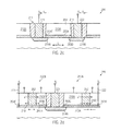
- FIG. 2 a schematically illustrates a top view of a semiconductor device 200 , which may comprise an appropriate substrate (not shown in FIG. 2 a ), which may include a piezoelectric material as explained above.
- the semiconductor device 200 may comprise one or more active regions 210 A, 210 B, which may be understood as semiconductor regions having or receiving an appropriate dopant profile therein in order to obtain at least one PN junction for controlling a current flow in the semiconductor material.
- the active regions 210 A, 210 B which in one illustrative embodiment may represent a semiconductor material including a silicon species, possibly in combination with other components such as germanium and the like, may be laterally enclosed by an isolation structure 211 which, in one illustrative embodiment, may be provided in the form of a shallow trench isolation.
- the active regions 210 A, 210 B may represent a portion of circuit elements, such as transistors and the like, the performance of which may be adjusted on the basis of a strain created in the active regions 210 A, 210 B.
- a first circuit element 250 A may be formed on the basis of the active region 210 A and a second circuit element 250 B may be provided on the basis of the active region 210 B.
- the circuit element 250 A may comprise or receive a gate electrode structure 251 when the device 250 A represents a field effect transistor.
- a current flow direction in the active region 210 A may be defined as a horizontal direction in FIG. 2 a , also indicated as a length direction L.
- a strain component provided along the length direction L may result in an increase of hole mobility or electron mobility, depending on the type of strain or a specified crystallographic configuration.
- the semiconductor device 200 may further comprise a first contact element 221 and a second contact element 222 , which may extend to a certain depth so as to electrically connect to the piezoelectric material (not shown) so that an appropriate electric field may be established upon applying an appropriate voltage across the contact elements 221 , 222 .
- the elements 221 , 222 may be comprised of any appropriate material composition, for instance in the form of a doped semiconductor material, a metal silicide material, tungsten, aluminum and the like.
- the contact elements 221 , 222 may be formed within the isolation structure 211 , so that the piezoelectric material may be electrically accessed without connecting to the active region 210 A, 210 B. In this case, a magnitude and type of strain may be individually adjusted for the active region 210 A, irrespective of any voltages applied to the active region 210 A.
- FIG. 2 b schematically illustrates a cross-sectional view of the semiconductor device 200 during a manufacturing stage in which the contact elements 221 , 222 ( FIG. 2 a ) may be formed within the isolation structure 211 ( FIG. 2 a ).
- the semiconductor device 200 may comprise a substrate 201 comprising a carrier material 202 , a buried insulating layer comprising a piezoelectric material 203 and a semiconductor layer 204 .
- the substrate 201 may have any configuration, as is also previously explained with reference to the substrate 101 .
- the semiconductor layer 204 may comprise a trench 212 that extends to and, in the embodiment shown, through the piezoelectric material layer 203 so as to connect to the carrier material 202 , which may comprise a crystalline semiconductor material.
- an implantation mask 213 may be formed above the semiconductor layer 204 so as to expose a portion of the trench 212 , for instance along a width direction, i.e., a direction perpendicular to the drawing plane of FIG. 2 b and corresponding to a vertical direction in FIG. 2 a , so as to connect to the entire width of the piezoelectric material 203 .
- a width direction i.e., a direction perpendicular to the drawing plane of FIG. 2 b and corresponding to a vertical direction in FIG. 2 a
- the mask 213 may be asymmetric with respect to the trench length 212 if electrical contact is to be established to a portion 203 A only, while not connecting to a portion 203 B. It should be appreciated that any other contact regime may be established, depending on the desired controllability of strain conditions in the active regions 210 A, 210 B ( FIG. 2 a ).
- the semiconductor device 200 as illustrated in FIG. 2 b may be formed on the basis of the following processes. After providing the substrate 201 , the trench 212 may be formed by using well-established patterning techniques involving sophisticated lithography and etch techniques.
- the process may be controlled by using the piezoelectric material layer 203 as an etch stop or etch control material, for instance by detecting specific atomic species released into the etch ambient and the like.
- additional insulating materials such as silicon dioxide, silicon nitride and the like, may be provided in combination with the piezoelectric material 203 so that established etch characteristics of these materials may be taken advantage of during the corresponding etch process.
- the implantation mask 213 may be provided, for instance in the form of a resist mask, and may be patterned in accordance with appropriate lithography techniques using a lithography mask including respective mask features for exposing the desired portion of the trench 212 .
- an implantation process 215 may be performed to incorporate an implantation species 214 so as to provide a desired enhanced degree of conductivity.
- the corresponding dopant species in the implantation region 214 may reliably connect to the portion 203 A after respective anneal processes, as indicated by the dashed line 214 A, thereby forming a contact portion 203 C for connecting to the piezoelectric material 203 A.
- the further processing may be continued by removing the mask 213 and filling the trench 212 with any appropriate dielectric material, such as silicon dioxide and the like.
- the further processing may be continued by forming circuit elements, such as transistors, in and above the active regions 210 A, 210 B ( FIG.
- the contacts 221 , 222 may be formed, for instance when forming contact elements to the active regions when forming substrate contacts and the like.
- any well-established process technique may be used.
- FIG. 2 c schematically illustrates the semiconductor device 200 in a further advanced manufacturing stage.
- the contact elements 221 , 222 may be formed in the isolation structure 211 , wherein the contact element 221 may connect to contact portion 203 C via the implantation region 214 A.
- the contact element 222 may connect to a second contact portion 203 D of the piezoelectric material 203 A via a corresponding implantation region 214 A.
- the contact elements 221 , 222 may be connected to any appropriate voltage source, an electric field may be established within the material 203 A, which substantially uniformly extends along the length direction within the material 203 A and may thus result in a corresponding mechanical deformation, which in turn may result in a desired magnitude and type of strain within the active region 210 A.
- the strain conditions in the active region 210 A may be individually adjustable by the contact elements 221 , 222 in order to appropriately adjust performance of any circuit element formed in and above the active region 210 A.
- FIG. 2 d schematically illustrates a cross-sectional view of the semiconductor device 200 in which the strain conditions in the active regions 210 B, 210 A may be individually adjusted on the basis of the piezoelectric materials 203 B, 203 A by providing an appropriate contact structure, which may include the contact elements 221 , 222 and at least one further contact element 223 .
- the contact element 221 may be used as a combined contact element so as to connect to both the piezoelectric material 203 A and the material 203 B via the contact portion 203 C and a corresponding contact portion 203 E. It should be appreciated, however, that, in other cases, separate contact elements may be provided to connect to the contact portion 203 E, if desired.
- the contact element 223 may connect to a contact portion 203 F so that the desired voltage may be applied across the contact elements 223 , 221 to induce a certain type of strain 210 T in the active region 210 B, as previously explained.
- the active region 210 B may represent a part of the circuit element 250 B in which the increase of the electron mobility in a specific zone 252 , such as a channel region, may result in enhanced device performance.
- the voltage across the contact elements 223 , 221 may be appropriately selected so as to obtain the strain component 210 T in the form of a tensile strain component.
- the active region 210 A may represent a part of the circuit element 250 A in which a specific zone 252 may result in enhanced performance upon creating a compressive strain component.
- the voltage across the contacts 221 , 222 may be selected such that the electric field in the material 203 A may result in a compressive strain component 210 C.
- FIG. 2 e schematically illustrates a cross-sectional view of the semiconductor device 200 when exposed to an etch ambient 217 in order to form the trench 212 on the basis of an etch mask 216 .
- this process 217 may be performed on the basis of well-established etch techniques, wherein appropriate endpoint detection techniques and the like may be used upon exposing the piezoelectric material 203 .
- the etch process 217 may be continued so as to etch through the layer 203 and a further insulating material may be provided, for instance a silicon dioxide material, which may act as an etch control layer.
- FIG. 2 f schematically illustrates the semiconductor device 200 in a further advanced manufacturing stage, i.e., after etching through the layer 203 and filling the trench 212 ( FIG. 2 e ) with an appropriate dielectric material so as to provide the isolation structure 211 .
- the isolation structure 211 may be formed on the basis of a high degree of compatibility with conventional process techniques, thereby providing the active regions 210 A, 210 B and the corresponding material layers 203 A, 203 B as “islands” that are separated by the structure 211 .
- FIG. 2 g schematically illustrates the semiconductor device 200 in a further advanced manufacturing stage.
- the circuit elements 250 A, 250 B formed on the basis of the active regions 210 A, 210 B may represent transistor elements, the performance of which may be adjusted on the basis of specific strain conditions, as described above.
- the transistors 250 A, 250 B may represent field effect transistors comprising a gate electrode structure 251 , which may include a gate insulation layer 251 D that separates a gate electrode material 251 A from the channel region 252 .
- the gate electrode structure 251 may comprise additional components, such as a metal silicide 251 C, spacer structure 254 and the like, if required.
- the gate electrode structure 251 may comprise a high-k dielectric material, i.e., the dielectric material having a dielectric constant of approximately 10.0 and higher, which may be included in the gate insulation layer 251 D.
- the electrode material 251 A may comprise a metal-containing material that may be in contact with the gate insulation layer 251 D.
- the transistors 250 A, 250 B may comprise drain and source regions 253 , which may be separated by the channel region 252 .
- the transistor 250 A may represent a transistor requiring a tensile strain component 252 T, while the transistor 250 B may represent a transistor requiring a compressive strain component 252 C.
- the transistors 250 A, 250 B may represent an N-channel transistor and a P-channel transistor, respectively. It should be appreciated that in other cases the transistors 250 A, 250 B may require the same type of strain, however, with a different magnitude and the like.
- the drain and source regions 253 may extend down to the corresponding piezoelectric materials 203 A, 203 B, thereby providing an appropriate contact regime in order to generate an electric field, at least temporarily, within the materials 203 A, 203 B according to the corresponding supply voltages supplied to drain and source regions 253 .
- one of the drain and source regions 253 may receive the supply voltage V dd
- the other one of the drain and source regions 253 may receive ground potential at a specific operational state.
- the strain component 252 T may be established within the channel region 252 of the transistor 250 A, which may result in an enhanced performance, at least as long as the corresponding voltage may drop across the drain and source regions 253 .
- the transistor 250 B in the form of a P-channel transistor may receive the supply voltage V dd and the ground potential, thereby inducing the compressive strain component 252 C, since the electric field in the material 203 B is of opposite direction compared to the electric field in the material 203 A with respect to the supply voltages as illustrated in FIG. 2 g .
- performance of the transistor 250 B may be enhanced, at least as long as a corresponding voltage drop may exist across the drain and source regions 253 .
- a positive voltage applied to the gate electrode structure 251 may thus result in the creation of a conductive channel, which may have an enhanced conductivity due to the presence of the tensile strain component 252 T, as long as a sufficient voltage drop exists across the drain and source regions 253 . Consequently, in this case, the transistor 250 A may have an increased drive current capability so as to achieve an increased switching speed.
- the transistor 250 B may also have superior performance, at least during a corresponding switching event.
- the transistors 250 A, 250 B may be formed on the basis of any well-established manufacturing technique, wherein, however, contrary to conventional strategies, different strain conditions may be established by using a single material in the form of the layers 203 A, 203 B without requiring complex separate process strategies for the transistors 250 A, 250 B. It should be appreciated, however, that, if required, other strain-inducing mechanisms may be implemented in one or both of the transistors 250 A, 250 B.
- a strain-inducing semiconductor alloy may be embedded into the active regions 210 A, 210 B, for instance by forming cavities therein and depositing an appropriate semiconductor alloy, as is previously described.
- strain-inducing dielectric materials may be formed above one or both of the transistors 250 A, 250 B in accordance with well-established stress engineering techniques. In this manner, respective “static” or “permanent” strain conditions may be established in one or both of the transistors 250 A, 250 B, while the mechanism based on the material layer 203 A, 203 B may provide an efficient modulation of the static strain conditions.
- the present disclosure provides semiconductor devices, substrates for forming the same and methods of operating the semiconductor device, in which a piezoelectric material may be used for adjusting the strain conditions within circuit elements, such as field effect transistors.
- a piezoelectric material may be used for adjusting the strain conditions within circuit elements, such as field effect transistors.
- an appropriate piezoelectric material may be provided in close proximity to the active semiconductor region, such as a channel region, and upon application of an appropriate voltage, a strain component may be established, which may be accomplished in a controllable manner or which may depend on the operational status of a circuit element formed in and above the semiconductor region under consideration. Consequently, different types of strain may be implemented into circuit elements, such as field effect transistors, on the basis of a single manufacturing regime, thereby significantly reducing the complexity of the overall manufacturing process.
Abstract
Description
Claims (17)
Priority Applications (1)
| Application Number | Priority Date | Filing Date | Title |
|---|---|---|---|
| US14/502,428 US9263582B2 (en) | 2009-02-27 | 2014-09-30 | Strain engineering in semiconductor devices by using a piezoelectric material |
Applications Claiming Priority (3)
| Application Number | Priority Date | Filing Date | Title |
|---|---|---|---|
| DE102009010843.2A DE102009010843B4 (en) | 2009-02-27 | 2009-02-27 | Substrates and semiconductor devices fabricated using a deformation technology using a piezoelectric material and methods of using such a deformation technology |
| DE102009010843.2 | 2009-02-27 | ||
| DE102009010843 | 2009-02-27 |
Related Child Applications (1)
| Application Number | Title | Priority Date | Filing Date |
|---|---|---|---|
| US14/502,428 Division US9263582B2 (en) | 2009-02-27 | 2014-09-30 | Strain engineering in semiconductor devices by using a piezoelectric material |
Publications (2)
| Publication Number | Publication Date |
|---|---|
| US20100219719A1 US20100219719A1 (en) | 2010-09-02 |
| US8884379B2 true US8884379B2 (en) | 2014-11-11 |
Family
ID=42666730
Family Applications (2)
| Application Number | Title | Priority Date | Filing Date |
|---|---|---|---|
| US12/711,322 Expired - Fee Related US8884379B2 (en) | 2009-02-27 | 2010-02-24 | Strain engineering in semiconductor devices by using a piezoelectric material |
| US14/502,428 Active US9263582B2 (en) | 2009-02-27 | 2014-09-30 | Strain engineering in semiconductor devices by using a piezoelectric material |
Family Applications After (1)
| Application Number | Title | Priority Date | Filing Date |
|---|---|---|---|
| US14/502,428 Active US9263582B2 (en) | 2009-02-27 | 2014-09-30 | Strain engineering in semiconductor devices by using a piezoelectric material |
Country Status (2)
| Country | Link |
|---|---|
| US (2) | US8884379B2 (en) |
| DE (1) | DE102009010843B4 (en) |
Cited By (1)
| Publication number | Priority date | Publication date | Assignee | Title |
|---|---|---|---|---|
| US10734531B2 (en) | 2017-06-22 | 2020-08-04 | The Penn State Research Foundation | Two-dimensional electrostrictive field effect transistor (2D-EFET) |
Families Citing this family (4)
| Publication number | Priority date | Publication date | Assignee | Title |
|---|---|---|---|---|
| FR2965658A1 (en) * | 2010-10-04 | 2012-04-06 | St Microelectronics Crolles 2 | Integrated device, has semiconductor layer formed on semiconductor substrate with interposition of insulating stack, where insulating stack has dielectric layer formed between piezoelectric layer and semiconductor layer |
| US10014331B2 (en) * | 2016-03-31 | 2018-07-03 | Skyworks Solutions, Inc. | Field-effect transistor devices having proximity contact features |
| CN109920844A (en) * | 2019-03-26 | 2019-06-21 | 电子科技大学 | A kind of insulated-gate type piezoelectricity field effect transistor |
| US11296224B1 (en) * | 2021-06-16 | 2022-04-05 | Purdue Research Foundation | Non-volatile polarization induced strain coupled 2D FET memory |
Citations (4)
| Publication number | Priority date | Publication date | Assignee | Title |
|---|---|---|---|---|
| US20060278903A1 (en) | 2005-05-31 | 2006-12-14 | Kabushiki Kaisha Toshiba | Semiconductor device with electrostrictive layer in semiconductor layer and method of manufacturing the same |
| US7230435B2 (en) * | 2003-01-21 | 2007-06-12 | Renesas Technology Corp. | Capacitance measurement circuit |
| US7453108B2 (en) * | 2006-05-09 | 2008-11-18 | Kabushiki Kaisha Toshiba | Semiconductor device that is advantageous in complex stress engineering and method of manufacturing the same |
| US7586158B2 (en) * | 2005-07-07 | 2009-09-08 | Infineon Technologies Ag | Piezoelectric stress liner for bulk and SOI |
Family Cites Families (7)
| Publication number | Priority date | Publication date | Assignee | Title |
|---|---|---|---|---|
| DE1277374B (en) * | 1964-09-30 | 1968-09-12 | Hitachi Ltd | Mechanical-electrical converter |
| US3463973A (en) * | 1967-09-12 | 1969-08-26 | Rca Corp | Insulating ferroelectric gate adaptive resistor |
| US3585415A (en) * | 1969-10-06 | 1971-06-15 | Univ California | Stress-strain transducer charge coupled to a piezoelectric material |
| US6596570B2 (en) * | 2001-06-06 | 2003-07-22 | International Business Machines Corporation | SOI device with reduced junction capacitance |
| US6884702B2 (en) * | 2002-06-04 | 2005-04-26 | Advanced Micro Devices, Inc. | Method of making an SOI semiconductor device having enhanced, self-aligned dielectric regions in the bulk silicon substrate |
| KR100682964B1 (en) * | 2006-02-09 | 2007-02-15 | 삼성전자주식회사 | Method for forming piezoelectric actuator of inkjet head |
| US7550330B2 (en) * | 2006-11-29 | 2009-06-23 | International Business Machines Corporation | Deep junction SOI MOSFET with enhanced edge body contacts |
-
2009
- 2009-02-27 DE DE102009010843.2A patent/DE102009010843B4/en not_active Expired - Fee Related
-
2010
- 2010-02-24 US US12/711,322 patent/US8884379B2/en not_active Expired - Fee Related
-
2014
- 2014-09-30 US US14/502,428 patent/US9263582B2/en active Active
Patent Citations (4)
| Publication number | Priority date | Publication date | Assignee | Title |
|---|---|---|---|---|
| US7230435B2 (en) * | 2003-01-21 | 2007-06-12 | Renesas Technology Corp. | Capacitance measurement circuit |
| US20060278903A1 (en) | 2005-05-31 | 2006-12-14 | Kabushiki Kaisha Toshiba | Semiconductor device with electrostrictive layer in semiconductor layer and method of manufacturing the same |
| US7586158B2 (en) * | 2005-07-07 | 2009-09-08 | Infineon Technologies Ag | Piezoelectric stress liner for bulk and SOI |
| US7453108B2 (en) * | 2006-05-09 | 2008-11-18 | Kabushiki Kaisha Toshiba | Semiconductor device that is advantageous in complex stress engineering and method of manufacturing the same |
Non-Patent Citations (1)
| Title |
|---|
| Translation of Official Communication from German Patent Office for German Patent Application No. 10 2009 010 843.2 dated Nov. 10, 2009. |
Cited By (2)
| Publication number | Priority date | Publication date | Assignee | Title |
|---|---|---|---|---|
| US10734531B2 (en) | 2017-06-22 | 2020-08-04 | The Penn State Research Foundation | Two-dimensional electrostrictive field effect transistor (2D-EFET) |
| US10964824B2 (en) | 2017-06-22 | 2021-03-30 | The Penn State Research Foundation | Two-dimensional electrostrictive field effect transistor (2D-EFET) |
Also Published As
| Publication number | Publication date |
|---|---|
| DE102009010843A1 (en) | 2010-11-11 |
| US20100219719A1 (en) | 2010-09-02 |
| US9263582B2 (en) | 2016-02-16 |
| DE102009010843B4 (en) | 2014-04-10 |
| US20150054083A1 (en) | 2015-02-26 |
Similar Documents
| Publication | Publication Date | Title |
|---|---|---|
| TWI387009B (en) | Technique for reducing crystal defects in strained transistors by tilted preamorphization | |
| US7329571B2 (en) | Technique for providing multiple stress sources in NMOS and PMOS transistors | |
| US7964458B2 (en) | Method for forming a strained transistor by stress memorization based on a stressed implantation mask | |
| US7547610B2 (en) | Method of making a semiconductor device comprising isolation trenches inducing different types of strain | |
| US8039878B2 (en) | Transistor having a channel with tensile strain and oriented along a crystallographic orientation with increased charge carrier mobility | |
| US20110269278A1 (en) | Stress Memorization with Reduced Fringing Capacitance Based on Silicon Nitride in MOS Semiconductor Devices | |
| US7932166B2 (en) | Field effect transistor having a stressed contact etch stop layer with reduced conformality | |
| US20110080772A1 (en) | Body Controlled Double Channel Transistor and Circuits Comprising the Same | |
| US7833874B2 (en) | Technique for forming an isolation trench as a stress source for strain engineering | |
| US9263582B2 (en) | Strain engineering in semiconductor devices by using a piezoelectric material | |
| US8062952B2 (en) | Strain transformation in biaxially strained SOI substrates for performance enhancement of P-channel and N-channel transistors | |
| US7999326B2 (en) | Tensile strain source using silicon/germanium in globally strained silicon | |
| US7754555B2 (en) | Transistor having a channel with biaxial strain induced by silicon/germanium in the gate electrode | |
| US7482219B2 (en) | Technique for creating different mechanical strain by a contact etch stop layer stack with an intermediate etch stop layer | |
| US8334569B2 (en) | Transistor with embedded Si/Ge material having enhanced across-substrate uniformity | |
| US8030148B2 (en) | Structured strained substrate for forming strained transistors with reduced thickness of active layer | |
| US8329531B2 (en) | Strain memorization in strained SOI substrates of semiconductor devices | |
| US7763515B2 (en) | Transistor with embedded silicon/germanium material on a strained semiconductor on insulator substrate | |
| US20130295767A1 (en) | Increased transistor performance by implementing an additional cleaning process in a stress liner approach | |
| KR20100078341A (en) | Method for fabricating a semiconductor | |
| WO2008042144A2 (en) | A semiconductor device comprising isolation trenches inducing different types of strain | |
| WO2007130240A1 (en) | A transistor having a channel with tensile strain and oriented along a crystallographic orientation with increased charge carrier mobility |
Legal Events
| Date | Code | Title | Description |
|---|---|---|---|
| AS | Assignment |
Owner name: GLOBALFOUNDRIES INC., CAYMAN ISLANDS Free format text: ASSIGNMENT OF ASSIGNORS INTEREST;ASSIGNORS:KRONHOLZ, STEPHAN;WIATR, MACIEJ;REEL/FRAME:024130/0401 Effective date: 20100302 |
|
| STCF | Information on status: patent grant |
Free format text: PATENTED CASE |
|
| MAFP | Maintenance fee payment |
Free format text: PAYMENT OF MAINTENANCE FEE, 4TH YEAR, LARGE ENTITY (ORIGINAL EVENT CODE: M1551) Year of fee payment: 4 |
|
| AS | Assignment |
Owner name: WILMINGTON TRUST, NATIONAL ASSOCIATION, DELAWARE Free format text: SECURITY AGREEMENT;ASSIGNOR:GLOBALFOUNDRIES INC.;REEL/FRAME:049490/0001 Effective date: 20181127 |
|
| AS | Assignment |
Owner name: GLOBALFOUNDRIES INC., CAYMAN ISLANDS Free format text: RELEASE BY SECURED PARTY;ASSIGNOR:WILMINGTON TRUST, NATIONAL ASSOCIATION;REEL/FRAME:054479/0842 Effective date: 20200410 Owner name: TAIWAN SEMICONDUCTOR MANUFACTURING CO., LTD., TAIWAN Free format text: ASSIGNMENT OF ASSIGNORS INTEREST;ASSIGNOR:GLOBALFOUNDRIES INC.;REEL/FRAME:054482/0862 Effective date: 20200515 |
|
| AS | Assignment |
Owner name: GLOBALFOUNDRIES INC., CAYMAN ISLANDS Free format text: RELEASE BY SECURED PARTY;ASSIGNOR:WILMINGTON TRUST, NATIONAL ASSOCIATION;REEL/FRAME:054636/0001 Effective date: 20201117 |
|
| FEPP | Fee payment procedure |
Free format text: MAINTENANCE FEE REMINDER MAILED (ORIGINAL EVENT CODE: REM.); ENTITY STATUS OF PATENT OWNER: LARGE ENTITY |
|
| LAPS | Lapse for failure to pay maintenance fees |
Free format text: PATENT EXPIRED FOR FAILURE TO PAY MAINTENANCE FEES (ORIGINAL EVENT CODE: EXP.); ENTITY STATUS OF PATENT OWNER: LARGE ENTITY |
|
| STCH | Information on status: patent discontinuation |
Free format text: PATENT EXPIRED DUE TO NONPAYMENT OF MAINTENANCE FEES UNDER 37 CFR 1.362 |
|
| FP | Lapsed due to failure to pay maintenance fee |
Effective date: 20221111 |