US8871652B2 - Method of manufacturing a semiconductor template - Google Patents
Method of manufacturing a semiconductor template Download PDFInfo
- Publication number
- US8871652B2 US8871652B2 US13/834,996 US201313834996A US8871652B2 US 8871652 B2 US8871652 B2 US 8871652B2 US 201313834996 A US201313834996 A US 201313834996A US 8871652 B2 US8871652 B2 US 8871652B2
- Authority
- US
- United States
- Prior art keywords
- microstructures
- patterned
- semiconductor
- substrate
- buffer layer
- Prior art date
- Legal status (The legal status is an assumption and is not a legal conclusion. Google has not performed a legal analysis and makes no representation as to the accuracy of the status listed.)
- Active, expires
Links
Images


Classifications
-
- H01L21/0243—
-
- H—ELECTRICITY
- H10—SEMICONDUCTOR DEVICES; ELECTRIC SOLID-STATE DEVICES NOT OTHERWISE PROVIDED FOR
- H10P—GENERIC PROCESSES OR APPARATUS FOR THE MANUFACTURE OR TREATMENT OF DEVICES COVERED BY CLASS H10
- H10P14/00—Formation of materials, e.g. in the shape of layers or pillars
- H10P14/20—Formation of materials, e.g. in the shape of layers or pillars of semiconductor materials
- H10P14/29—Formation of materials, e.g. in the shape of layers or pillars of semiconductor materials characterised by the substrates
- H10P14/2924—Structures
- H10P14/2925—Surface structures
-
- H—ELECTRICITY
- H10—SEMICONDUCTOR DEVICES; ELECTRIC SOLID-STATE DEVICES NOT OTHERWISE PROVIDED FOR
- H10P—GENERIC PROCESSES OR APPARATUS FOR THE MANUFACTURE OR TREATMENT OF DEVICES COVERED BY CLASS H10
- H10P14/00—Formation of materials, e.g. in the shape of layers or pillars
- H10P14/20—Formation of materials, e.g. in the shape of layers or pillars of semiconductor materials
- H10P14/29—Formation of materials, e.g. in the shape of layers or pillars of semiconductor materials characterised by the substrates
- H10P14/2901—Materials
-
- H—ELECTRICITY
- H10—SEMICONDUCTOR DEVICES; ELECTRIC SOLID-STATE DEVICES NOT OTHERWISE PROVIDED FOR
- H10P—GENERIC PROCESSES OR APPARATUS FOR THE MANUFACTURE OR TREATMENT OF DEVICES COVERED BY CLASS H10
- H10P14/00—Formation of materials, e.g. in the shape of layers or pillars
- H10P14/20—Formation of materials, e.g. in the shape of layers or pillars of semiconductor materials
- H10P14/32—Formation of materials, e.g. in the shape of layers or pillars of semiconductor materials characterised by intermediate layers between substrates and deposited layers
- H10P14/3202—Materials thereof
- H10P14/3214—Materials thereof being Group IIIA-VA semiconductors
- H10P14/3216—Nitrides
-
- H—ELECTRICITY
- H10—SEMICONDUCTOR DEVICES; ELECTRIC SOLID-STATE DEVICES NOT OTHERWISE PROVIDED FOR
- H10P—GENERIC PROCESSES OR APPARATUS FOR THE MANUFACTURE OR TREATMENT OF DEVICES COVERED BY CLASS H10
- H10P14/00—Formation of materials, e.g. in the shape of layers or pillars
- H10P14/20—Formation of materials, e.g. in the shape of layers or pillars of semiconductor materials
- H10P14/34—Deposited materials, e.g. layers
- H10P14/3402—Deposited materials, e.g. layers characterised by the chemical composition
- H10P14/3414—Deposited materials, e.g. layers characterised by the chemical composition being group IIIA-VIA materials
- H10P14/3416—Nitrides
-
- H—ELECTRICITY
- H10—SEMICONDUCTOR DEVICES; ELECTRIC SOLID-STATE DEVICES NOT OTHERWISE PROVIDED FOR
- H10H—INORGANIC LIGHT-EMITTING SEMICONDUCTOR DEVICES HAVING POTENTIAL BARRIERS
- H10H20/00—Individual inorganic light-emitting semiconductor devices having potential barriers, e.g. light-emitting diodes [LED]
- H10H20/01—Manufacture or treatment
- H10H20/011—Manufacture or treatment of bodies, e.g. forming semiconductor layers
- H10H20/013—Manufacture or treatment of bodies, e.g. forming semiconductor layers having light-emitting regions comprising only Group III-V materials
- H10H20/0133—Manufacture or treatment of bodies, e.g. forming semiconductor layers having light-emitting regions comprising only Group III-V materials with a substrate not being Group III-V materials
- H10H20/01335—Manufacture or treatment of bodies, e.g. forming semiconductor layers having light-emitting regions comprising only Group III-V materials with a substrate not being Group III-V materials the light-emitting regions comprising nitride materials
-
- H—ELECTRICITY
- H10—SEMICONDUCTOR DEVICES; ELECTRIC SOLID-STATE DEVICES NOT OTHERWISE PROVIDED FOR
- H10H—INORGANIC LIGHT-EMITTING SEMICONDUCTOR DEVICES HAVING POTENTIAL BARRIERS
- H10H20/00—Individual inorganic light-emitting semiconductor devices having potential barriers, e.g. light-emitting diodes [LED]
- H10H20/80—Constructional details
- H10H20/81—Bodies
- H10H20/819—Bodies characterised by their shape, e.g. curved or truncated substrates
Definitions
- the present invention relates to a method of manufacturing a semiconductor template and more particularly, relates to a method of manufacturing a semiconductor template by attracting strains by means of microstructures.
- Nitride HEMTs on a sapphire substrate has been applied to X-band (8-12 GHz).
- X-band 8-12 GHz.
- the corresponding gate length is shortened, which results in the self-heating effect in Nitride HEMTs under the operations of high frequency, high bias voltage, high current, high power, and especially in high frequency band.
- the thermal conductivity of sapphire substrates is lower (0.4 Wcm ⁇ 1 K ⁇ 1 )
- the heat generated by the Nitride HEMTs is accumulated in the transistor, and thus the self-heating effect will limit the performance of transistors and cause damages.
- the thermal conductivity of a sapphire substrate is 0.4 Wcm ⁇ 1 K ⁇ 1 while the thermal conductivity of a SiC substrate is 4.9 Wcm ⁇ 1 K ⁇ 1 and the thermal conductivity of a Si substrate is 1.5 Wcm ⁇ 1 K ⁇ 1 —both of them have higher thermal conductivity than the sapphire substrate and thus are favored by being the substrates of high-power and high-speed GaN-based devices.
- a high-power and high-speed GaN-based device including a SiC substrate has high performance in device characteristics, the costs on SiC substrates are too high. In consideration of costs on substrates, Si substrates are cheaper than SiC substrates and sapphire substrates.
- LEDs have many advantages such as lower energy consumption, longer lifetime, faster reaction speed, etc.; therefore, LEDs have been gradually replacing traditional lights such as bulbs and fluorescent lamps.
- the luminous efficiency of LEDs has been a target that manufacturers go for.
- the luminous flux of LEDs is inspected all the time during the whole process of manufacturing so as to confirm whether the luminous efficiency of LEDs meets the expectation.
- blue LED chips are utilized as excitation sources by white LEDs in the market.
- Most blue LED chips include GaN or InGaN as primary materials for light emitting, and blue LED chips include GaN-based epitaxial layer depositing on sapphire substrates.
- GaN-based epitaxial layer and sapphire substrate have the same crystal structure of hexagonal close-packed lattice form.
- the sapphire substrate is patterned. Owing to the use of ordered arrangement of patterns in the sapphire substrate, internal quantum efficiency is improved, and light extraction efficiency is increased. As a result, the brightness of LEDs is enhanced.
- the lattice constant and the thermal conductivity of GaN-based epitaxial layer and of sapphire substrates are not matching.
- the mismatch in the lattice constant of GaN-based epitaxial layers and that of sapphire substrate is up to 16%. Therefore, if GaN-based epitaxial layers are deposited on a sapphire substrate, defects such as point defects, dislocation defects and cracks are generated due to the partial relaxation of strains in GaN-based epitaxial layers.
- GaN-based epitaxial layers When different substrates can be used to grow GaN-based epitaxial layers, users can either choose a SiC substrate or a Si substrate. In the consideration of costs, utilization of Si substrates in LEDs will be the mainstream in the future. However, the mismatches in lattice constant and in thermal conductivity between the GaN-based epitaxial layer and the Si substrate are greater than that between the GaN-based epitaxial layer and the sapphire substrate, which makes it even more difficult to grow GaN-based epitaxial layers on Si substrates without defects.
- a method for manufacturing a semiconductor template balanced between strains and defects is provided according to embodiments of the present invention to avoid defects generated due to mismatches in lattice constant and in thermal conductivity between the GaN-based epitaxial layer and the substrate.
- a method for manufacturing a semiconductor template balanced between strains and defects utilizes microstructures to accumulate strains toward the outside of a first patterned zones, to reduce the residual strains in the first patterned zones, and to avoid generating defects in the first patterned zones.
- a method for manufacturing a semiconductor template balanced between strains and defects including: preparing a substrate, dividing the substrate into a plurality of first patterned zones and a plurality of second patterned zones, the second patterned zones applied to separate the first patterned zones; selecting a semiconductor with an ideal lattice of a semiconductor buffer layer to be deposited on the substrate; etching a plurality of first microstructures in the first patterned zones according to the semiconductor with an ideal lattice, the first microstructures and the semiconductor with the ideal lattice following a lattice-structure matching relationship, discovered by strain-traction experiments, making the substrate a multi-patterned substrate; and depositing the semiconductor buffer layer having the semiconductor with the ideal lattice on the multi-patterned substrate to manufacture a semiconductor template which is balanced between strains and defects.
- the semiconductor buffer layer is affected by the difference between a strain-traction force in the semiconductor with the ideal lattice on the first patterned zones and in a semiconductor with a lattice on the second patterned zones; owing to the lower lattice-constant mismatch in the semiconductor buffer layer grown on the first microstructures, the residual strains in the semiconductor buffer layer are accumulated toward the outside of the first patterned zones; as a result, the strains in the semiconductor buffer layer on the first patterned zones are relaxed.
- the method further includes the second patterned zones being connected so the first patterned zones are disposed into an array among the second patterned zones.
- the method further includes etching the first microstructures within the height of 0.3-10 ⁇ m in the first patterned zones.
- the photolithography process is selected from the group of UV lithography, laser interference lithography, holographic lithography, E-beam lithography, X-ray lithography, Nano lithography and Nano imprinting; the etching process is selected from the group of wet etching and dry etching.
- the area of the first patterned zones is less than 4 cm 2 .
- Materials of the semiconductor buffer layer are selected from the group of Carbon, Silicon and Germanium.
- the semiconductor buffer layer includes a compound semiconductor having materials selected from the group of Group III-V, Group II-VI and Group III-VI of the periodic table.
- the defects are selected from the group of point defects, dislocation defects and cracks.
- embodiments of the present invention describe method including dividing the substrate into the first patterned zones and the second patterned zones; forming a plurality of microstructures in the first patterned zones; thus, when depositing the semiconductor buffer layer on the substrate, the method utilizes microstructures to accumulate strains toward the outside of the first patterned zones, to reduce the residual strains in the first patterned zones, and to avoid generating defects in the first patterned zones.
- FIG. 1 is a schematic view of a substrate provided according to a first embodiment of the present invention.
- FIG. 2A is a cross-sectional view of crossing along A-A line in FIG. 1 .
- FIG. 2C is a cross-sectional view showing exposing the photoresist layer to light so the photoresist layer is patterned corresponding to first microstructures.
- FIG. 2D is a cross-sectional view showing etching the hard mask layer with the shades of the photoresist layer so the hard mask layer is patterned corresponding to the first microstructures.
- FIG. 2E is a cross-sectional view showing etching the first microstructures in the substrate with the shades of the hard mask layer.
- FIG. 3 is a schematic view of a multi-patterned substrate according to the first embodiment of the present invention.
- FIG. 4 is a cross-sectional view showing depositing a semiconductor buffer layer on the multi-patterned substrate to manufacture a semiconductor template that is balanced between strains and defects according to the first embodiment of the present invention.
- FIG. 5 is a cross-sectional view showing a defectless epitaxial substrate after removing the second patterned zones according to the first embodiment of the present invention.
- FIG. 6 is a schematic view of a multi-patterned substrate according to a second embodiment of the present invention.
- FIG. 7 is a cross-sectional view of the multi-patterned substrate according to the second embodiment of the present invention.
- FIG. 8 is a cross-sectional view of a multi-patterned substrate according to a third embodiment of the present invention.
- FIG. 9 is an electron microscope image of a semiconductor template according to an embodiment of the present invention.
- FIG. 10 is an optical microscope image of a semiconductor template according to an embodiment of the present invention.
- FIG. 11 is a diagram showing a room temperature photoluminescence (PL) spectrum of InGaN-based LEDs grown on the semiconductor template of FIG. 10 and on a conventional polished sapphire substrate.
- PL room temperature photoluminescence
- FIG. 12 is a diagram showing shifts of PL peak energy versus excitation power density of InGaN-based LEDs grown on the semiconductor template of FIG. 10 and on a conventional polished sapphire substrate.
- FIG. 13 is a diagram showing the PL peak intensity versus excitation power density of InGaN-based LEDs grown on the semiconductor template of FIG. 10 and on a conventional polished sapphire substrate.
- the present invention relates to a method of manufacturing a semiconductor template balanced between strains and defects.
- numerous details are set forth in order to provide a thorough understanding of the present invention. It will be appreciated by one skilled in the art that variations of these specific details are possible while still achieving the results of the present invention. In other instance, well-known components are not described in detail in order not to unnecessarily obscure the present invention.
- a method includes: preparing a substrate 1 ; dividing the substrate into a plurality of first patterned zones 11 (only one is identified with referential number in the figure) and a plurality of second patterned zones 12 (only one is identified with referential number in the figure).
- the substrate 11 is selected from the group of a SiC substrate, a Si substrate, a GaAs substrate, a GaN substrate, an InAs substrate, and a sapphire substrate.
- the second patterned zones 12 are connected as grid shaped and the first patterned zones 11 are disposed into an array among the second patterned zones 12 .
- the area of the first patterned zones is less than 4 cm 2 .
- the method then includes: selecting a semiconductor with an ideal lattice of a semiconductor buffer layer 3 (illustrated in FIG. 4 ) to be deposited. (By “ideal,” here it means there is no strain existing in the lattice of the semiconductor buffer layer.) Given the materials of the semiconductor buffer layer 3 include GaN, the semiconductor with the ideal lattice has a hexagonal close-packed lattice structure.
- FIG. 2A is a cross-sectional view along the A-A line in FIG. 1 .
- FIG. 2B is a cross-sectional view showing forming a hard mask layer and a photoresist layer on the substrate.
- FIG. 2C is a cross-sectional view showing exposing the photoresist layer to light, including electrons, so that the photoresist layer is patterned corresponding to the first microstructures 2 .
- FIG. 2D is a cross-sectional view showing etching the hard mask layer with the shades of the photoresist layer so that the hard mask layer is patterned corresponding to the first microstructures.
- FIG. 2E is a cross-sectional view showing etching the substrate with the shades of the hard mask layer so that the first microstructures 1 is formed in the first patterned zones, and the second patterned zones remain blank.
- the method can be summarized as follows.
- a hard mask layer 200 and a photoresist layer 300 are formed on the substrate 1 .
- a photolithography process is performed.
- the photolithography process means exposing the photoresist layer 300 to light, including electrons, so as to pattern the photoresist layer 300 in the first patterned zones 11 .
- the photoresist layer 300 is selected from the group of positive photoresist and negative photoresist.
- the difference between two photoresists lies in: when the photoresist layer 300 is positive photoresist, the portion of the photoresist that is exposed to light becomes soluble to photoresist developer, and the portion of the photoresist that is unexposed remains insoluble to photoresist developer; when the photoresist layer 300 is negative photoresist, the portion of the photoresist that is exposed to light becomes insoluble to the photoresist developer, and the unexposed portion of the photoresist is dissolved by photoresist developer.
- first microstructures In order to acquire a semiconductor with an ideal lattice on a first patterned zones, the design of first microstructures needs to follow a lattice-structure matching relationship, discovered by the strain-traction experiments as shown in FIG. 8 to FIG. 13 . Therefore, after the deposition of the semiconductor buffer, strains, which are generated due to the mismatches in lattice constant and in thermal conductivity between the semiconductor buffer layer 3 and the substrate 1 , are accumulated toward the outside of the first patterned zones 11 . Areas outside the first pattern zones 11 includes an interval interface between the first patterned zone 11 and the second patterned zone 12 and includes areas inside the second patterned zones 12 .
- the height 21 of the first microstructures is 0.3-10 ⁇ m, and the protrusive shape of the first microstructures 2 is selected from the group of rod, cone and pyramid.
- the photolithography process is selected from the group of UV lithography, laser interference lithography, holographic lithography, E-beam lithography, X-ray lithography, Nano lithography and Nano imprinting.
- the etching process is selected from the group of wet etching and dry etching. Wet etching includes etching the first patterned zones 11 with an etching solution, and dry etching includes etching the first patterned zones 11 with an ICP-RIE (Inductively Coupled Plasma Reactive Ion Etching) or an RIE (Reactive Ion Etching).
- the photolithography process can be performed directly on the first patterned zones 11 and the second patterned zones 12 as follows.
- the photoresist layer 300 is formed on the first patterned zones 11 and the second patterned zones 12 .
- the photoresist layer 300 on the first patterned zones 11 is exposed to light according to the positions of first microstructures 2 .
- the unexposed photoresist (Here is the negative photoresist, which means the unexposed photoresist is solved) on the first patterned zones 11 and second patterned zones 12 is solved so that the patterns of first patterned zones 11 reveal (i.e. a developing step).
- the patterns of photoresist layer are transferred to the substrate by an etching process to form a plurality of the first microstructures in the first patterned zones, and the second patterned zones remain blank.
- Ways of forming the first microstructures 2 with photolithography process and etching process are common techniques in the field and are not mentioned more here.
- FIG. 3 is a schematic view of a multi-patterned substrate according to the first embodiment of the present invention.
- the first microstructures 2 are formed in the first patterned zones 11 .
- the semiconductor with the ideal lattice has a hexagonal close-packed lattice structure.
- the first microstructures 2 are arranged in the first patterned zones 11 with the hexagonal close-packed lattice cycle, which is defined as a first cycle P1.
- P1 is the first cycle
- n is a positive integer
- A is a lattice constant of the semiconductor buffer layer
- P1′ ⁇ abs(nA)*0.15.
- the ratio value which is defined as the height 21 of the first microstructures divided by the distance between the first microstructures, is larger than 1.
- the first microstructures 2 can be arranged in a square lattice cycle.
- FIG. 4 is a cross-sectional view showing depositing a semiconductor buffer layer on the multi-patterned substrate to manufacture a semiconductor template which is balanced between strains and defects according to the first embodiment of the present invention.
- the additional method can be summarized as follows.
- the semiconductor buffer layer 3 having the semiconductor with a ideal lattice is deposited on the multi-patterned substrate 1 ′.
- the first microstructures 2 and the semiconductor with the ideal lattice need to follow a lattice-structure matching relationship, discovered by the strain-traction experiments. Therefore, a semiconductor template 100 balanced between strains and defects is manufactured.
- Materials of the semiconductor buffer layer 3 are selected from the group of Carbon, Silicon and Germanium; for example, C, Si, Ge, SiC or SiGe.
- the semiconductor buffer layer 3 also includes a compound semiconductor having materials selected from the group of Group III-V, Group II-VI and Group III-VI of the periodic table; for example, GaN, AlN, AlGaN, AlInGaN, GaAs, AlGaAs or GaAsP.
- the semiconductor buffer layer is affected by the difference between a strain-traction force in the semiconductor with the ideal lattice on the first patterned zones and in a semiconductor with a lattice on the second patterned zones; owing to the lower lattice-constant mismatch in the semiconductor buffer layer grown on the first microstructures, the residual strains in the semiconductor buffer layer are accumulated toward the outside of the first patterned zones; as a result, the strains in the semiconductor buffer layer on the first patterned zones are relaxed.
- a semiconductor template 100 which is balanced between strains and defects is manufactured.
- the semiconductor buffer layer 3 when the semiconductor buffer layer 3 is deposited on a multi-patterned substrate, the semiconductor buffer layer with a better lattice would grow along with the protrusive shape of the first microstructures rather than the blank in the second patterned zones, and subsequently the lattice of the semiconductor buffer layer on the first patterned zones is close to an ideal lattice.
- the strains which are generated from the lattice constant mismatch and different thermal conductivity between the semiconductor buffer layer 3 and the substrate 1 , are accumulated toward the outside of the first patterned zones 11 , and thus the defects 31 are generated toward the outside of the first patterned zones 11 .
- the defects 31 include point defects, dislocation defects, or cracks.
- FIG. 5 is a cross-sectional view showing a defectless epitaxial substrate after removing the second patterned zones according to the first embodiment of the present invention.
- a plurality of defect-accumulated areas 12 ′ and a plurality of strain-relaxed areas 11 ′ corresponding to the second patterned zones 12 and the first patterned zones 11 on the semiconductor template 100 , respectively, are found.
- the additional method is removing the defect-accumulated areas 12 ′, and thus the strain-relaxed areas 11 ′ are being a plurality of defectless epitaxial substrates 100 ′.
- FIG. 6 is a schematic view of a multi-patterned substrate according to a second embodiment of the present invention
- FIG. 7 is a cross-sectional view of the multi-patterned substrate according to the second embodiment of the present invention.
- the multi-patterned substrate 1 a is similar to the multi-patterned substrate 1 ′, but a plurality of the second microstructures 4 a are formed in the second patterned zones 12 with the photolithography process and the etching process on the multi-patterned substrate 1 a .
- the second microstructures 4 a are arranged in a second cycle P2, which is different from the first cycle.
- the formula of the second cycle is: P 2 ⁇ 10*( nA ) ⁇ P 2′,
- P2 is the second cycle
- n is a positive integer
- A is a lattice constant of the semiconductor buffer layer
- P2′ ⁇ abs(10*(nA)).
- the height 41 a of the protrusion of the second microstructures 4 a is lower than the height 21 a of the protrusion of the first microstructures 2 a , and the difference in the protrusive height between the first microstructures and the second microstructures is within 0.05-10 ⁇ m. Furthermore, in order to discriminate the area ratio of the second microstructures 4 a in one unit cell in the second patterned zone from that of the first microstructures 2 a in one unit cell in the first patterned zone 11 , the air-duty cycle, which is defined as the area of the second microstructures 4 a in one unit cell in the second patterned zone divided by the area of the second patterned zone, is used.
- the air-duty cycle in the second patterned zones 12 is under 20%; according to other embodiments of the present invention, the air-duty cycle of the second microstructures 4 a in the second patterned zones 12 can be more than 80%.
- the semiconductor buffer layer with a better lattice would grow along with the higher protrusive shape of the first microstructures rather than the lower protrusive shape of the second microstructures. Therefore, the lattice of the semiconductor buffer layer on the first patterned zones is close to an ideal lattice.
- the strains, which are generated due to the lattice constant mismatch and different thermal conductivity between the semiconductor buffer layer and the multi-patterned substrate 1 a are accumulated toward the outside of the first patterned zones 11 .
- FIG. 8 a cross-sectional view of a multi-patterned substrate according to a third embodiment of the present invention.
- the multi-patterned substrate 1 b is provided according to the third embodiment of the present invention.
- the multi-patterned substrate 1 b is similar to the multi-patterned substrate 1 ′, but a plurality of second microstructures 4 b are formed in the second patterned zones 12 with the photolithography process and the etching process on the multi-patterned substrate 1 b ; the second microstructures 4 a are arranged in a second cycle, which is different from the first cycle.
- the formula of the second cycle is: P 2 ⁇ 10*( nA ) ⁇ P 2′,
- P2 is the second cycle
- n is a positive integer
- A is a lattice constant of the semiconductor buffer layer
- P2′ ⁇ abs(10*(nA)).
- the shape of second microstructures 4 b are depression, and the distance from the lowest point of the second microstructures 4 b to the highest point of the first microstructures 2 b is within 0.2-10 ⁇ m. Furthermore, in order to discriminate the area ratio of the second microstructures in one unit cell in the second patterned zone from that of the first microstructures 2 a in one unit cell in the first patterned zone 11 , the air-duty cycle is used. According to one embodiment of the present invention, the air-duty cycle of the second microstructures 4 b in the second patterned zones 12 is under 20%; according to other embodiments of the present invention, the air-duty cycle of the second microstructures 4 b in the second patterned zones 12 can be more than 80%.
- the semiconductor buffer layer with a better lattice would grow along with the higher protrusive shape of the first microstructure rather than the second microstructures with the shape of depression. Therefore, the lattice of the semiconductor buffer layer on the first patterned zones is close to an ideal lattice. As a result, the strains, which are generated due to the lattice constant mismatch and different thermal conductivity between the semiconductor buffer layer and the multi-patterned substrate 1 a , are accumulated toward the outside of the first patterned zones 11 .
- FIG. 9 shows a secondary electron microscope image of a InGaN-based LED grown on the semiconductor template, which is according to the first embodiment of the present invention.
- the semiconductor template consists of a GaN-based semiconductor buffer layer and a multi-patterned sapphire substrate.
- the corresponding multi-patterned substrate comprises first microstructures in the first patterned zone with the area of 600 ⁇ m ⁇ 600 ⁇ m, and the blank in the second patterned zone (i.e. the outside of the first patterned zone).
- the first microstructures have the shape of the protrusion, the first cycle P1 of 500 nm, the height of about 550 nm and the 30% air-duty cycle. As induced by the strain-traction force, dislocation defects are observed in the interval interface between the first patterned zone and the second patterned zone.
- FIG. 10 shows an optical microscope image of a InGaN-based LED grown on the semiconductor template, which is according to a first embodiment of the present invention.
- the semiconductor template consists of a GaN-based semiconductor buffer layer and a multi-patterned sapphire substrate.
- the corresponding multi-patterned substrate comprises first microstructures in the first patterned zone with the area of 600 ⁇ m ⁇ 600 ⁇ m, and the blank in the second patterned zone (i.e. the outside of the first patterned zone).
- the first microstructures have the shape of the protrusion, the first cycle P1 of 500 nm, the height of about 550 nm and the 50% air-duty cycle. As induced by the strain-traction force, cracks are observed outside the first patterned zone.
- FIG. 11 shows a room temperature photoluminescence (PL) spectrum of InGaN-based LEDs grown on the semiconductor template of FIG. 10 and on a conventional polished sapphire substrate.
- the semiconductor template consists of a GaN-based semiconductor buffer layer and a multi-patterned sapphire substrate.
- the InGaN-based LEDs with the semiconductor template of FIG. 10 and the conventional polished sapphire substrate were grown under the same growth conditions.
- curve C1 corresponds to the PL spectrum of the InGaN-based LED grown on the semiconductor template in the first patterned zones
- curve C2 corresponds to the PL spectrum of the InGaN-based LED grown on the conventional polished sapphire substrate
- curve C3 corresponds to the PL spectrum of the InGaN-based LED grown on the semiconductor template in the second patterned zone (i.e. the outside of the first patterned zone). Due to the proper design of the first microstructures in the first patterned zones, the residual strains in the semiconductor buffer layer are accumulated toward the outside of the first patterned zones (i.e. the second patterned zone), and thus the defects are generated toward the outside of the first patterned zones.
- FIG. 12 shows the shifts of PL peak energy versus excitation power density of InGaN-based LEDs grown on the semiconductor template of FIG. 10 and on a conventional polished sapphire substrate.
- C4 and C5 are the curves showing shifts of PL peak energy corresponding to the InGaN-based LEDs as shown in curve C1 and C2 in FIG. 11 , respectively.
- the shifts of PL peak energy through the InGaN-based LED grown on the semiconductor template in the first patterned zones i.e. C4
- the sample grown on the conventional polished sapphire substrate i.e.
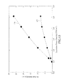
- FIG. 13 shows the PL peak intensity versus excitation power density of InGaN-based LEDs grown on the semiconductor template of FIG. 10 and on a conventional polished sapphire substrate.
- C6 and C7 are curves showing the PL peak intensity corresponding to the InGaN-based LEDs as shown in curve C1 and C2 in FIG. 11 .
- the much more linear enhancement of the PL peak intensity of the InGaN-based LED grown on the semiconductor template in the first patterned zones i.e. C6
- the saturation behavior is shown in the PL peak intensity of the InGaN-based LED grown on the conventional polished sapphire substrate (i.e. C5) under high excitation power. It is attributed to the Quantum-Confined Stark Effect significantly within the multiple quantum wells.
- the method includes forming the first microstructures in the first patterned zones of the substrate; thus, when depositing the semiconductor buffer layer on the substrate, the strains, which are generated due to the mismatches in lattice constant and in thermal conductivity between the semiconductor buffer layer and the substrate, are attracted toward the outside of the first patterned zones.
- the first microstructures and second microstructures having difference are formed corresponding to the first patterned zones and the second patterned zones.
- strains which are generated due to the mismatches in lattice constant and in thermal conductivity between the semiconductor buffer layer and the substrate, are attracted toward the outside of the first patterned zones.
- the difference between the first microstructures and second microstructures includes height, cycle, or area ratio.
- substrate utilized in embodiments of the present invention is selected from the group of SiC substrate, Si substrate and sapphire substrate, which is different from the materials of the semiconductor buffer layer (the semiconductor buffer layer includes a compound semiconductor having materials selected from the group of Group III-V, Group II-VI and Group III-VI of the periodic table).
Landscapes
- Led Devices (AREA)
Abstract
Description
P1=nA±P1′
P2≧10*(nA)±P2′,
P2≧10*(nA)±P2′,
Claims (15)
Applications Claiming Priority (3)
| Application Number | Priority Date | Filing Date | Title |
|---|---|---|---|
| TW101144726A TWI473295B (en) | 2012-11-29 | 2012-11-29 | Method for manufacturing semiconductor template with equalization between stress and defect |
| TW101144726A | 2012-11-29 | ||
| TW101144726 | 2012-11-29 |
Publications (2)
| Publication Number | Publication Date |
|---|---|
| US20140147991A1 US20140147991A1 (en) | 2014-05-29 |
| US8871652B2 true US8871652B2 (en) | 2014-10-28 |
Family
ID=50773654
Family Applications (1)
| Application Number | Title | Priority Date | Filing Date |
|---|---|---|---|
| US13/834,996 Active 2033-04-05 US8871652B2 (en) | 2012-11-29 | 2013-03-15 | Method of manufacturing a semiconductor template |
Country Status (2)
| Country | Link |
|---|---|
| US (1) | US8871652B2 (en) |
| TW (1) | TWI473295B (en) |
Cited By (1)
| Publication number | Priority date | Publication date | Assignee | Title |
|---|---|---|---|---|
| EP3696300A1 (en) | 2019-02-18 | 2020-08-19 | Aixatech GmbH | Method for the production of a body made of composite material, especially for use in the manufacture of electronic or optoelectronic components |
Families Citing this family (4)
| Publication number | Priority date | Publication date | Assignee | Title |
|---|---|---|---|---|
| DE102018116783B4 (en) | 2017-09-29 | 2024-05-08 | Taiwan Semiconductor Manufacturing Co., Ltd. | Semiconductor substrate and method for manufacturing the same |
| US20190103267A1 (en) * | 2017-09-29 | 2019-04-04 | Taiwan Semiconductor Manufacturing Co., Ltd. | Semiconductor substrate and method of manufacturing thereof |
| CN112507653B (en) * | 2020-10-27 | 2022-10-21 | 南京理工大学 | IV-V group two-dimensional semiconductor model construction method with better electron transport performance |
| TWI757170B (en) * | 2021-05-10 | 2022-03-01 | 友達光電股份有限公司 | Light emitting device and method of light emitting chip mass transfer |
Citations (3)
| Publication number | Priority date | Publication date | Assignee | Title |
|---|---|---|---|---|
| US20050196925A1 (en) * | 2003-12-22 | 2005-09-08 | Kim Sang H. | Method of forming stress-relaxed SiGe buffer layer |
| US20070020874A1 (en) * | 2005-07-22 | 2007-01-25 | Ya-Hong Xie | Method for controlling dislocation positions in silicon germanium buffer layers |
| US20120235161A1 (en) * | 2008-05-06 | 2012-09-20 | Tanya Paskova | Group iii nitride templates and related heterostructures, devices, and methods for making them |
-
2012
- 2012-11-29 TW TW101144726A patent/TWI473295B/en not_active IP Right Cessation
-
2013
- 2013-03-15 US US13/834,996 patent/US8871652B2/en active Active
Patent Citations (3)
| Publication number | Priority date | Publication date | Assignee | Title |
|---|---|---|---|---|
| US20050196925A1 (en) * | 2003-12-22 | 2005-09-08 | Kim Sang H. | Method of forming stress-relaxed SiGe buffer layer |
| US20070020874A1 (en) * | 2005-07-22 | 2007-01-25 | Ya-Hong Xie | Method for controlling dislocation positions in silicon germanium buffer layers |
| US20120235161A1 (en) * | 2008-05-06 | 2012-09-20 | Tanya Paskova | Group iii nitride templates and related heterostructures, devices, and methods for making them |
Cited By (1)
| Publication number | Priority date | Publication date | Assignee | Title |
|---|---|---|---|---|
| EP3696300A1 (en) | 2019-02-18 | 2020-08-19 | Aixatech GmbH | Method for the production of a body made of composite material, especially for use in the manufacture of electronic or optoelectronic components |
Also Published As
| Publication number | Publication date |
|---|---|
| US20140147991A1 (en) | 2014-05-29 |
| TWI473295B (en) | 2015-02-11 |
| TW201421730A (en) | 2014-06-01 |
Similar Documents
| Publication | Publication Date | Title |
|---|---|---|
| US8871652B2 (en) | Method of manufacturing a semiconductor template | |
| CN101814564B (en) | Method for preparing epitaxial growing nano pattern substrate of nitride | |
| CN104221168B (en) | The method for manufacturing the nano-patterning base material for high efficiency nitride light-emitting diode | |
| KR101238169B1 (en) | Method of manufacturing light emitting diode using wet etched type buffer layer | |
| US9000414B2 (en) | Light emitting diode having heterogeneous protrusion structures | |
| KR101023135B1 (en) | Semiconductor light emitting device having a substrate having a biconcave-convex structure and a manufacturing method thereof | |
| US20150333223A1 (en) | Reversely-Installed Photonic Crystal LED Chip and Method for Manufacturing Same | |
| JP5306779B2 (en) | Light emitting device and manufacturing method thereof | |
| US20150064821A1 (en) | Method for fabricating nano-patterned substrate for high-efficiency nitride-based light-emitting diode | |
| CN103311097A (en) | Method for manufacturing micro-nano graph on sapphire substrate | |
| TW202030891A (en) | Concave patterned substrate structure, semiconductor device with heat dissipation enhancement, and manufacturing method of the semiconductor device using the concave patterned substrate structure | |
| Zhang et al. | The improvement of GaN-based light-emitting diodes using nanopatterned sapphire substrate with small pattern spacing | |
| Xu et al. | Preparation of dome-shaped SiO 2/Al 2 O 3 composite-patterned sapphire substrate for high-performance mini-LED backlight modules | |
| TW201236190A (en) | LED epitaxial structure and manufacturing method | |
| US20130126929A1 (en) | Method for manufacturing nano-imprint mould, method for manufacturing light-emitting diode using the nano imprint mould manufactured thereby, and light-emitting diode manufactured thereby | |
| CN103904175B (en) | There is the manufacture method of waveguiding structure photonic crystal light-emitting diode | |
| CN205385037U (en) | Ultraviolet gan base led epitaxial structure | |
| US20110254019A1 (en) | Adapted semiconductor light emitting device and method for manufacturing the same | |
| CN107482094A (en) | LED based on GaN-based axial nanorod array and its preparation method | |
| CN115148873B (en) | Method for preparing semiconductor device | |
| Ogiya et al. | Improvement of LED luminance efficiency by sapphire nano PSS etching | |
| CN103682005B (en) | LED epitaxial growth processing procedure | |
| KR101244298B1 (en) | Method of manufacturing Light Emitting Diode using Heat Treatment and Light Emitting Diode of formed by using the same | |
| TWM365362U (en) | Structural improvement of patterned sapphire substrate and light emitting device | |
| CN116364824A (en) | A deep ultraviolet light emitting diode |
Legal Events
| Date | Code | Title | Description |
|---|---|---|---|
| AS | Assignment |
Owner name: KINGWAVE CORPORATION, TAIWAN Free format text: ASSIGNMENT OF ASSIGNORS INTEREST;ASSIGNORS:KUAN, CHIEH-HSIUNG;SU, WEN-SHENG;REEL/FRAME:030046/0600 Effective date: 20130314 |
|
| STCF | Information on status: patent grant |
Free format text: PATENTED CASE |
|
| MAFP | Maintenance fee payment |
Free format text: PAYMENT OF MAINTENANCE FEE, 4TH YR, SMALL ENTITY (ORIGINAL EVENT CODE: M2551) Year of fee payment: 4 |
|
| MAFP | Maintenance fee payment |
Free format text: PAYMENT OF MAINTENANCE FEE, 8TH YR, SMALL ENTITY (ORIGINAL EVENT CODE: M2552); ENTITY STATUS OF PATENT OWNER: SMALL ENTITY Year of fee payment: 8 |
|
| AS | Assignment |
Owner name: JAMHO ENTERPRISE CO., LTD., TAIWAN Free format text: ASSIGNMENT OF ASSIGNORS INTEREST;ASSIGNOR:KINGWAVE CORPORATION;REEL/FRAME:068694/0637 Effective date: 20240912 |