US8859413B2 - Method of growing gan crystal on silicon substrate, and light emitting device and method of manufacturing thereof - Google Patents
Method of growing gan crystal on silicon substrate, and light emitting device and method of manufacturing thereof Download PDFInfo
- Publication number
- US8859413B2 US8859413B2 US12/073,097 US7309708A US8859413B2 US 8859413 B2 US8859413 B2 US 8859413B2 US 7309708 A US7309708 A US 7309708A US 8859413 B2 US8859413 B2 US 8859413B2
- Authority
- US
- United States
- Prior art keywords
- gan
- layer
- nano
- silicon substrate
- electrode
- Prior art date
- Legal status (The legal status is an assumption and is not a legal conclusion. Google has not performed a legal analysis and makes no representation as to the accuracy of the status listed.)
- Active, expires
Links
Images


Classifications
-
- H01L21/02381—
-
- H—ELECTRICITY
- H10—SEMICONDUCTOR DEVICES; ELECTRIC SOLID-STATE DEVICES NOT OTHERWISE PROVIDED FOR
- H10P—GENERIC PROCESSES OR APPARATUS FOR THE MANUFACTURE OR TREATMENT OF DEVICES COVERED BY CLASS H10
- H10P14/00—Formation of materials, e.g. in the shape of layers or pillars
- H10P14/20—Formation of materials, e.g. in the shape of layers or pillars of semiconductor materials
- H10P14/29—Formation of materials, e.g. in the shape of layers or pillars of semiconductor materials characterised by the substrates
- H10P14/2901—Materials
- H10P14/2902—Materials being Group IVA materials
- H10P14/2905—Silicon, silicon germanium or germanium
-
- H01L21/02488—
-
- H01L21/02491—
-
- H01L21/0254—
-
- H01L21/02639—
-
- H01L21/02645—
-
- H01L33/007—
-
- H01L33/12—
-
- H—ELECTRICITY
- H10—SEMICONDUCTOR DEVICES; ELECTRIC SOLID-STATE DEVICES NOT OTHERWISE PROVIDED FOR
- H10H—INORGANIC LIGHT-EMITTING SEMICONDUCTOR DEVICES HAVING POTENTIAL BARRIERS
- H10H20/00—Individual inorganic light-emitting semiconductor devices having potential barriers, e.g. light-emitting diodes [LED]
- H10H20/01—Manufacture or treatment
- H10H20/011—Manufacture or treatment of bodies, e.g. forming semiconductor layers
- H10H20/013—Manufacture or treatment of bodies, e.g. forming semiconductor layers having light-emitting regions comprising only Group III-V materials
- H10H20/0133—Manufacture or treatment of bodies, e.g. forming semiconductor layers having light-emitting regions comprising only Group III-V materials with a substrate not being Group III-V materials
- H10H20/01335—Manufacture or treatment of bodies, e.g. forming semiconductor layers having light-emitting regions comprising only Group III-V materials with a substrate not being Group III-V materials the light-emitting regions comprising nitride materials
-
- H—ELECTRICITY
- H10—SEMICONDUCTOR DEVICES; ELECTRIC SOLID-STATE DEVICES NOT OTHERWISE PROVIDED FOR
- H10H—INORGANIC LIGHT-EMITTING SEMICONDUCTOR DEVICES HAVING POTENTIAL BARRIERS
- H10H20/00—Individual inorganic light-emitting semiconductor devices having potential barriers, e.g. light-emitting diodes [LED]
- H10H20/80—Constructional details
- H10H20/81—Bodies
- H10H20/815—Bodies having stress relaxation structures, e.g. buffer layers
-
- H—ELECTRICITY
- H10—SEMICONDUCTOR DEVICES; ELECTRIC SOLID-STATE DEVICES NOT OTHERWISE PROVIDED FOR
- H10P—GENERIC PROCESSES OR APPARATUS FOR THE MANUFACTURE OR TREATMENT OF DEVICES COVERED BY CLASS H10
- H10P14/00—Formation of materials, e.g. in the shape of layers or pillars
- H10P14/20—Formation of materials, e.g. in the shape of layers or pillars of semiconductor materials
- H10P14/27—Formation of materials, e.g. in the shape of layers or pillars of semiconductor materials using selective deposition, e.g. simultaneous growth of monocrystalline and non-monocrystalline semiconductor materials
- H10P14/271—Formation of materials, e.g. in the shape of layers or pillars of semiconductor materials using selective deposition, e.g. simultaneous growth of monocrystalline and non-monocrystalline semiconductor materials characterised by the preparation of substrate for selective deposition
- H10P14/274—Formation of materials, e.g. in the shape of layers or pillars of semiconductor materials using selective deposition, e.g. simultaneous growth of monocrystalline and non-monocrystalline semiconductor materials characterised by the preparation of substrate for selective deposition using seed materials
-
- H—ELECTRICITY
- H10—SEMICONDUCTOR DEVICES; ELECTRIC SOLID-STATE DEVICES NOT OTHERWISE PROVIDED FOR
- H10P—GENERIC PROCESSES OR APPARATUS FOR THE MANUFACTURE OR TREATMENT OF DEVICES COVERED BY CLASS H10
- H10P14/00—Formation of materials, e.g. in the shape of layers or pillars
- H10P14/20—Formation of materials, e.g. in the shape of layers or pillars of semiconductor materials
- H10P14/32—Formation of materials, e.g. in the shape of layers or pillars of semiconductor materials characterised by intermediate layers between substrates and deposited layers
- H10P14/3202—Materials thereof
- H10P14/3238—Materials thereof being insulating materials
-
- H—ELECTRICITY
- H10—SEMICONDUCTOR DEVICES; ELECTRIC SOLID-STATE DEVICES NOT OTHERWISE PROVIDED FOR
- H10P—GENERIC PROCESSES OR APPARATUS FOR THE MANUFACTURE OR TREATMENT OF DEVICES COVERED BY CLASS H10
- H10P14/00—Formation of materials, e.g. in the shape of layers or pillars
- H10P14/20—Formation of materials, e.g. in the shape of layers or pillars of semiconductor materials
- H10P14/32—Formation of materials, e.g. in the shape of layers or pillars of semiconductor materials characterised by intermediate layers between substrates and deposited layers
- H10P14/3202—Materials thereof
- H10P14/3241—Materials thereof being conductive materials
-
- H—ELECTRICITY
- H10—SEMICONDUCTOR DEVICES; ELECTRIC SOLID-STATE DEVICES NOT OTHERWISE PROVIDED FOR
- H10P—GENERIC PROCESSES OR APPARATUS FOR THE MANUFACTURE OR TREATMENT OF DEVICES COVERED BY CLASS H10
- H10P14/00—Formation of materials, e.g. in the shape of layers or pillars
- H10P14/20—Formation of materials, e.g. in the shape of layers or pillars of semiconductor materials
- H10P14/34—Deposited materials, e.g. layers
- H10P14/3402—Deposited materials, e.g. layers characterised by the chemical composition
- H10P14/3414—Deposited materials, e.g. layers characterised by the chemical composition being group IIIA-VIA materials
- H10P14/3416—Nitrides
-
- H01L33/20—
-
- H—ELECTRICITY
- H10—SEMICONDUCTOR DEVICES; ELECTRIC SOLID-STATE DEVICES NOT OTHERWISE PROVIDED FOR
- H10H—INORGANIC LIGHT-EMITTING SEMICONDUCTOR DEVICES HAVING POTENTIAL BARRIERS
- H10H20/00—Individual inorganic light-emitting semiconductor devices having potential barriers, e.g. light-emitting diodes [LED]
- H10H20/80—Constructional details
- H10H20/81—Bodies
- H10H20/819—Bodies characterised by their shape, e.g. curved or truncated substrates
Definitions
- Example embodiments are directed to a method of growing GaN single crystals on a silicon substrate, a method of manufacturing a GaN-based light emitting device using the silicon substrate, and a GaN-based light emitting device manufactured using the silicon substrate.
- Example embodiments include a method of growing GaN single crystals using a TiN group metal nitride as a buffer layer, a method of manufacturing a GaN-based light emitting device using a silicon substrate, and a GaN-based light emitting device manufactured using a silicon substrate.
- Nitride group semiconductors such as GaN may be used in light emitting devices, and examples of such light emitting devices include blue-violet light emitting diodes and laser diodes and electronic devices with higher switching speed and higher output.
- FIG. 1 is a cross-sectional view of an example embodiment of a conventional light emitting device 1 manufactured using a sapphire substrate.
- the light emitting device 1 may include a GaN buffer layer 12 , an n-GaN layer 14 , an active layer 16 , and a p-GaN layer 18 , for example, and these layers may be sequentially formed on a sapphire substrate 10 .
- a p-electrode 20 and an n-electrode 22 may be required to apply power in order to combine electrons and holes in the active layer 16 .
- the p-electrode 20 may be formed on the p-GaN layer 18 and the n-electrode 22 may be formed on the n-GaN layer 14 .
- a dry etching process or other like process for etching portions of regions of the p-GaN layer 18 and the active layer 16 may be performed to form the n-electrode 22 , because the sapphire substrate 10 may be non-conductive and otherwise it may not be possible to form an electrode on a lower surface of the sapphire substrate 10 .
- the sapphire substrate 10 can be replaced by a silicon substrate
- manufacturing costs may be reduced since the cost of the silicon substrate may be less than the sapphire substrate 10 , the SiC substrate, or other like substrate.
- a larger silicon substrate or other like substrate may be used in the above light emitting device 1 , and this may also achieve cost reduction.
- an electrode may be formed on a lower surface of the silicon substrate, and this may result in reduced manufacturing processes.
- a GaN light emitting device may not use a silicon substrate because thermal expansion may cause severe cracks to form between the silicon substrate and the GaN thin film layer.
- a method of using a buffer layer formed of AlN between the silicon substrate and the GaN thin film layer may address this problem.
- the higher electrical conductivity and higher thermal conductivity of the silicon substrate may not be utilized because the AlN layer has a lower electrical conductivity.
- Example embodiments provide a method of growing a GaN single crystal thin film on a silicon or other like substrate using a buffer layer formed of TiN or other like material that may have higher electrical conductivity and thermal conductivity, and a method of manufacturing a GaN-based light emitting device using a silicon substrate.
- Example embodiments also provide a GaN-based light emitting device including a silicon substrate.
- a method of growing GaN single crystals may include forming a buffer layer comprising a TiN group material on a silicon substrate, forming a nano-pattern comprising silicon oxide on the buffer layer, and growing GaN single crystals on buffer layer and the nano-pattern.
- Example embodiments provide a method of manufacturing a light emitting device that may include forming a buffer layer using a TiN group material on a silicon substrate, forming a nano-pattern using silicon oxide on the buffer layer, forming an n-GaN layer on the buffer layer and the nano-pattern, forming an active layer on the n-GaN layer, forming a p-GaN layer on the active layer, and forming a p-electrode and an n-electrode.
- Example embodiments also provide a light emitting device that may include a silicon substrate, a buffer layer formed of a TiN group material on the silicon substrate, a nano-pattern formed of SiO 2 on the buffer layer, an n-GaN layer formed on the buffer layer and the nano-pattern, an active layer formed on the n-GaN layer, and a p-GaN layer formed on the active layer.
- FIG. 1 is a schematic cross-sectional view of a structure of a conventional light emitting device manufactured using a sapphire substrate.
- FIGS. 2A through 2G are cross-sectional views illustrating a method of growing GaN single crystals according to example embodiments.
- FIGS. 3A through 3C are microscopic images of metal nano-clusters formed by annealing metal layers formed of Au to thicknesses of 50 ⁇ , 150 ⁇ , and 300 ⁇ , respectively, according to example embodiments.
- FIGS. 4A and 4B are graphs showing various characteristics of metal nano-clusters formed by annealing according to varying thicknesses of metal layers formed of Au according to example embodiments.
- FIG. 5 is a microscopic image of a metal nano-cluster formed of anodized aluminum oxide (MO) according to example embodiments.
- FIG. 6 is a microscopic image of a sample of GaN single crystals grown on a silicon substrate according to example embodiments.
- FIGS. 7 and 8 respectively are graphs showing XRD locking curves measured at (002) plane and (102) plane according to example embodiments.
- FIGS. 9A through 9D are cross-sectional views illustrating a method of manufacturing a GaN-based light emitting device, according to example embodiments.
- a silicon substrate 100 as a substrate for growing a GaN single crystal thin film thereon may be prepared.
- a buffer layer 120 may be formed on the silicon substrate 100 .
- the buffer layer 120 may be formed of a TiN group metal nitride or other like metal nitride having higher corrosion and erosion resistance, higher electrical conductivity, and higher adhesion.
- Other metal nitrides may include Al x Ti 1-x N, where 0 ⁇ x ⁇ 0.5, or Cr x Ti 1-x N, where 0 ⁇ x ⁇ 0.5, for example.
- the thickness of the buffer layer 120 may affect the growth of the GaN single crystal thin film.
- the thickness of the buffer layer 120 may be between 1 and 50 nm, for example, and the optimum thickness of the buffer layer 120 may be determined.
- a SiO 2 layer 140 and a metal layer 150 may be formed on the buffer layer 120 , and the SiO 2 layer 140 and the metal layer 150 may be sequentially formed on the buffer layer 120 , for example.
- the metal layer 150 may be formed of Au or other like metal.
- a metal nano-cluster 155 formed of a plurality of metal nano-dots may be formed by annealing the metal layer 150 .
- the density, width, and/or height of the metal nano-cluster 155 and of the gaps between the metal nano-dots may be controlled by the thickness and/or the annealing condition of the metal layer 150 .
- FIGS. 3A through 3C are microscopic images of metal nano-clusters according to example embodiments formed by annealing metal layers formed of Au to thicknesses of 50 ⁇ , 150 ⁇ , and 300 ⁇ , respectively, at a temperature of 600° C. for 1 minute under an air atmosphere.
- FIG. 4A is a graph showing the width of metal nano-dots of the metal nano-cluster and the distance between successive nano-dots according to the thicknesses of Au used as the metal layers 150 .
- FIG. 4B is a graph showing the height and density of the metal nano-dots of the metal nano-cluster according to the thicknesses of Au used as the metal layers 150 . Referring to FIGS.
- a nano-cluster with nano-dots having a width of 50 to 300 nm, a height of 10 to 160 nm, and gaps of 50 to 200 nm between the nano-dots may have a density of 5 to 100 ea/ ⁇ m 2 .
- the metal nano-cluster 155 may be formed by anodizing.
- the metal layer 150 may be formed of Al, and the metal nano-cluster 155 may be formed by anodizing the Al.
- FIG. 5 is a microscopic image of example embodiments of a metal nano-cluster 155 formed of anodized aluminum oxide (AAO).
- AAO anodized aluminum oxide
- the anodizing was performed at a temperature of 10° C. using 0.3M oxalic acid, and a pore widening process was performed at a temperature of 20° C. using 5.4 wt % phosphoric acid.
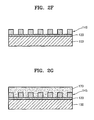
- a nano-pattern 145 formed of silicon oxide may be formed by dry etching the SiO 2 layer 140 using the metal nano-cluster 155 as a mask and stripping the metal nano-cluster 155 .
- Example embodiments of the process of forming the nano-pattern 145 using the metal nano-cluster 155 as a mask after the metal nano-cluster 155 is formed are described with reference to FIGS. 2C through 2F , although the nano-pattern 145 may be formed using a conventional photolithography process or other like process. However, forming the nano-pattern 145 using the metal nano-cluster 155 formed by annealing the metal layer 150 or using AAO as a mask may be economical and/or reduce manufacturing processes.
- GaN single crystals 170 may be grown from the buffer layer 120 over the nano-pattern 145 .
- TiN and GaN have a lattice constant difference (i.e., a rate of lattice mismatch) of approximately 6%, that is, d TIN ⁇ 220 ⁇ is 0.149 nm and d GAN ⁇ 11 — 20 ⁇ is 0.159 nm, and thus, the rate of lattice mismatch is approximately 6.3%. Accordingly, the rate of lattice mismatch of approximately 20% between silicon and GaN may be buffered.
- the buffer layer 120 is formed of AlN as in the prior art, d AlN ⁇ 11 — 20 ⁇ is 0.155 nm and d GAN ⁇ 11 — 20 ⁇ is 0.159 nm, and thus, the rate of lattice mismatch is approximately 2.5%. That is, the lattice constant difference (2.5%) between AlN and GaN is lower than lattice constant differences exhibited by example embodiments.
- the advantages of the silicon substrate having higher electrical conductivity may not be used.
- TiN has a lower resistivity and it may function with the silicon substrate.
- TiN has a thermal expansion coefficient between those of GaN and silicon and accordingly, the occurrence of cracks due to thermal expansion difference may be reduced when the GaN single crystals 170 are grown.
- SiO 2 is amorphous and may absorb stress transmitted to the GaN single crystals 170 .
- the GaN single crystals 170 may be formed over the nano-pattern 145 formed of SiO 2 , a similar effect to an epitaxial lateral overgrowth (ELOG) is possible.
- ELOG epitaxial lateral overgrowth
- higher quality GaN single crystals 170 having higher crystallinity may be grown, and for example, the GaN single crystals 170 grown between the adjacent nano-patterns 145 may have a defect density of greater than 10 9 ea/cm 2 .
- the GaN single crystals 170 grown above the nano-patterns 145 may have a defect density of approximately 10 6 to 10 7 ea/cm 2 .
- FIG. 6 is a microscopic image of example embodiments of GaN single crystals grown on a silicon substrate
- FIGS. 7 and 8 respectively are graphs showing XRD locking curves measured at (002) plane and (102) plane with respect to the GaN single crystals of FIG. 6
- the GaN single crystal has the buffer layer formed of TiN to a thickness of 20 nm, and the nano-pattern may be formed using the metal nano-cluster 155 formed of MO as a mask, for example.
- a full width at half maximum (FWHM) at (002) plane is approximately 377 arcsec
- that of at (102) plane is approximately 655 arcsec.
- FIGS. 9A through 9D are cross-sectional views illustrating a method of manufacturing the GaN-based light emitting device, according to example embodiments.
- a buffer layer 120 , a nano-pattern 145 formed of silicon oxide, and GaN single crystals 170 grown over the buffer layer 120 and the nano-pattern 145 may be formed on a silicon substrate 100 .
- the buffer layer 120 may be formed of a TiN group metal nitride or other like metal nitride, for example Al x Ti 1-x N where 0 ⁇ x ⁇ 0.5, or Cr x Ti 1-x N where 0 ⁇ x ⁇ 0.5.
- the nano-pattern 145 formed of silicon oxide may be formed using a metal nano-cluster formed by annealing a metal layer, or using AAO as a mask, or can be formed using a conventional photo lithography method or other like method.
- an n-GaN layer 175 may be formed by doping an n-type dopant in the GaN single crystals 170 , for example.
- an active layer 190 and a p-GaN layer 210 may be formed on the n-GaN layer 175 , and the active layer 190 and p-GaN layer 210 may be formed sequentially on the n-GaN layer 175 .
- the active layer 190 may be formed of a GaN-based Group III-V nitride semiconductor or the like.
- the active layer 190 may have a single quantum well structure or a multi-quantum well structure of InGaN/GaN, InGaN/InGaN, InGaN/AlGaN, or InGaN/InAlGaN or other like structure.
- the p-GaN layer 210 may be formed by doping a p-type dopant in a GaN layer after the GaN layer is formed, for example.
- a p-electrode 230 and an n-electrode 250 may be formed in a vertical electrode structure, and for example, the p-electrode 230 may be formed on the p-GaN layer 210 , and the n-electrode 250 may be formed on a lower surface of the silicon substrate 100 , although numerous example embodiments may be formed. As other example embodiments provide, the n-electrode 250 may be formed on exposed portions of the n-GaN layer 175 . The exposed portions of the n-GaN layer 175 may be formed by etching portions of the p-GaN layer 210 and the active layer 190 or other like process.
- Forming the p-electrode 230 and the n-electrode 250 in a vertical electrode structure may simplify manufacturing processes, and also may increase an effective area of the active layer 190 is increased. As example embodiments provide, increasing an effective area of the active layer 190 may increase light emission efficiency of the GaN-based light emitting device.
- TiN has a lower resistivity (approximately 15 ⁇ cm), and thus, the electrical conductivity of the silicon substrate 100 may be utilized.
- the p-electrode 230 and the n-electrode 250 formed in a vertical electrode structure may be adopted in the GaN-based light emitting device.
- a feature of a method of growing a GaN single crystal thin film according to example embodiments is using TiN which has a higher electrical and thermal conductivity. Thus, cracks generated during growing a GaN single crystal thin film can be reduced. Also, a higher quality GaN thin film having higher crystallinity may be grown by growing the GaN thin film on a silicon oxide film having a nano-pattern.
- a GaN-based light emitting device including a silicon substrate may have a lower manufacturing cost since the price of the silicon substrate may be less than the price of a sapphire substrate and the light emitting device may be formed using a larger diameter substrate. Using a larger diameter substrate in the light emitting device may increase productivity. Additionally, adopting a vertical electrode structure may reduce manufacturing processes and/or manufacturing costs.
Landscapes
- Led Devices (AREA)
Abstract
Description
Claims (7)
Applications Claiming Priority (2)
| Application Number | Priority Date | Filing Date | Title |
|---|---|---|---|
| KR1020070048309A KR100902512B1 (en) | 2007-05-17 | 2007-05-17 | Method for growing BaN single crystals on silicon substrate, manufacturing method of BaN-based light emitting devices and BaN-based light emitting devices |
| KR10-2007-0048309 | 2007-05-17 |
Publications (2)
| Publication Number | Publication Date |
|---|---|
| US20080283821A1 US20080283821A1 (en) | 2008-11-20 |
| US8859413B2 true US8859413B2 (en) | 2014-10-14 |
Family
ID=40026590
Family Applications (1)
| Application Number | Title | Priority Date | Filing Date |
|---|---|---|---|
| US12/073,097 Active 2031-07-29 US8859413B2 (en) | 2007-05-17 | 2008-02-29 | Method of growing gan crystal on silicon substrate, and light emitting device and method of manufacturing thereof |
Country Status (2)
| Country | Link |
|---|---|
| US (1) | US8859413B2 (en) |
| KR (1) | KR100902512B1 (en) |
Families Citing this family (37)
| Publication number | Priority date | Publication date | Assignee | Title |
|---|---|---|---|---|
| US8946674B2 (en) * | 2005-08-31 | 2015-02-03 | University Of Florida Research Foundation, Inc. | Group III-nitrides on Si substrates using a nanostructured interlayer |
| US20100176369A2 (en) * | 2008-04-15 | 2010-07-15 | Mark Oliver | Metalized Silicon Substrate for Indium Gallium Nitride Light-Emitting Diodes |
| US8154038B2 (en) * | 2008-07-01 | 2012-04-10 | Taiwan Semiconductor Manufacturing Co., Ltd | Group-III nitride for reducing stress caused by metal nitride reflector |
| KR101064082B1 (en) * | 2009-01-21 | 2011-09-08 | 엘지이노텍 주식회사 | Light emitting element |
| GB2467911B (en) * | 2009-02-16 | 2013-06-05 | Rfmd Uk Ltd | A semiconductor structure and a method of manufacture thereof |
| KR101040012B1 (en) * | 2009-03-16 | 2011-06-08 | 엘지이노텍 주식회사 | Semiconductor device manufacturing method |
| KR101055867B1 (en) | 2009-03-27 | 2011-08-11 | 한국표준과학연구원 | Gap Device Containing Metal Nanopoints |
| US8405068B2 (en) * | 2009-07-22 | 2013-03-26 | Rfmd (Uk) Limited | Reflecting light emitting structure and method of manufacture thereof |
| KR101650840B1 (en) * | 2009-08-26 | 2016-08-24 | 삼성전자주식회사 | Light emitting device and method of manufacturing the same |
| US8203153B2 (en) * | 2010-01-15 | 2012-06-19 | Koninklijke Philips Electronics N.V. | III-V light emitting device including a light extracting structure |
| KR101217210B1 (en) | 2010-10-07 | 2012-12-31 | 서울대학교산학협력단 | Light emitting device and method for manufacturing the same |
| CN102280545A (en) * | 2011-08-17 | 2011-12-14 | 中国科学院苏州纳米技术与纳米仿生研究所 | Silicon-based light emission device and method for making same |
| KR101867999B1 (en) | 2011-10-31 | 2018-06-18 | 삼성전자주식회사 | Method of forming III-V group material layer, semiconductor device comprising III-V group material layer and method of manufacturing the same |
| CN102610716A (en) * | 2012-03-31 | 2012-07-25 | 中国科学院半导体研究所 | Method for large-area manufacture of nano-gallium nitride patterned substrates |
| US9093420B2 (en) | 2012-04-18 | 2015-07-28 | Rf Micro Devices, Inc. | Methods for fabricating high voltage field effect transistor finger terminations |
| US9124221B2 (en) | 2012-07-16 | 2015-09-01 | Rf Micro Devices, Inc. | Wide bandwidth radio frequency amplier having dual gate transistors |
| US8988097B2 (en) | 2012-08-24 | 2015-03-24 | Rf Micro Devices, Inc. | Method for on-wafer high voltage testing of semiconductor devices |
| US9147632B2 (en) | 2012-08-24 | 2015-09-29 | Rf Micro Devices, Inc. | Semiconductor device having improved heat dissipation |
| US9142620B2 (en) | 2012-08-24 | 2015-09-22 | Rf Micro Devices, Inc. | Power device packaging having backmetals couple the plurality of bond pads to the die backside |
| US9917080B2 (en) | 2012-08-24 | 2018-03-13 | Qorvo US. Inc. | Semiconductor device with electrical overstress (EOS) protection |
| US9202874B2 (en) | 2012-08-24 | 2015-12-01 | Rf Micro Devices, Inc. | Gallium nitride (GaN) device with leakage current-based over-voltage protection |
| US9129802B2 (en) | 2012-08-27 | 2015-09-08 | Rf Micro Devices, Inc. | Lateral semiconductor device with vertical breakdown region |
| US9070761B2 (en) | 2012-08-27 | 2015-06-30 | Rf Micro Devices, Inc. | Field effect transistor (FET) having fingers with rippled edges |
| US9325281B2 (en) | 2012-10-30 | 2016-04-26 | Rf Micro Devices, Inc. | Power amplifier controller |
| MY164421A (en) * | 2012-12-06 | 2017-12-15 | Mimos Berhad | A method of producing vertical nanowires |
| CN104638068B (en) * | 2013-11-07 | 2018-08-24 | 上海蓝光科技有限公司 | A kind of substrat structure and preparation method thereof being used for the growth of III-V group-III nitride |
| US9455327B2 (en) | 2014-06-06 | 2016-09-27 | Qorvo Us, Inc. | Schottky gated transistor with interfacial layer |
| US9536803B2 (en) | 2014-09-05 | 2017-01-03 | Qorvo Us, Inc. | Integrated power module with improved isolation and thermal conductivity |
| US10062684B2 (en) | 2015-02-04 | 2018-08-28 | Qorvo Us, Inc. | Transition frequency multiplier semiconductor device |
| US10615158B2 (en) | 2015-02-04 | 2020-04-07 | Qorvo Us, Inc. | Transition frequency multiplier semiconductor device |
| US9496523B1 (en) * | 2015-06-19 | 2016-11-15 | Universal Display Corporation | Devices and methods to improve light outcoupling from an OLED array |
| US10431624B2 (en) * | 2015-07-08 | 2019-10-01 | Samsung Electronics Co., Ltd. | Method of manufacturing image sensor including nanostructure color filter |
| US9917156B1 (en) | 2016-09-02 | 2018-03-13 | IQE, plc | Nucleation layer for growth of III-nitride structures |
| WO2019040358A1 (en) * | 2017-08-22 | 2019-02-28 | Corning Incorporated | Glass article with transparent, light converting spatial location encoding layer |
| US11929446B2 (en) | 2021-12-30 | 2024-03-12 | Changchun University Of Science And Technology | Detector material and preparation method thereof |
| CN114300580B (en) * | 2021-12-30 | 2024-06-04 | 长春理工大学 | Detector material and preparation method thereof |
| CN120358782B (en) * | 2025-06-25 | 2025-09-19 | 深圳平湖实验室 | Gallium nitride device and method for manufacturing gallium nitride device |
Citations (9)
| Publication number | Priority date | Publication date | Assignee | Title |
|---|---|---|---|---|
| US20020068466A1 (en) * | 2000-12-06 | 2002-06-06 | Seung-Hwan Lee | Methods of forming thin films by atomic layer deposition |
| US20020197825A1 (en) * | 2001-03-27 | 2002-12-26 | Akira Usui | Semiconductor substrate made of group III nitride, and process for manufacture thereof |
| US20040106274A1 (en) * | 2002-11-21 | 2004-06-03 | International Business Machines Corporation | Gate structure with independently tailored vertical doping profile |
| US20050156180A1 (en) * | 2001-06-25 | 2005-07-21 | Zhibo Zhang | Optoelectronic devices having arrays of quantum-dot compound semiconductor superlattices therein |
| KR20050088960A (en) | 2005-08-12 | 2005-09-07 | 장구현 | Growth of single nitride-based semiconductor substrate and manufacturing of high-quality nitride-based light emitting devices |
| WO2006025793A1 (en) * | 2004-08-31 | 2006-03-09 | Agency For Science, Technology And Research | Nanostructures and method of making the same |
| US20060172512A1 (en) * | 2003-03-07 | 2006-08-03 | Kazumasa Hiramatsu | Substrate of gallium nitride single crystal and process for producing the same |
| KR20070011550A (en) | 2004-04-30 | 2007-01-24 | 나노시스, 인크. | Nanowire Growth and Acquisition Systems and Methods |
| US20070085093A1 (en) * | 2005-09-22 | 2007-04-19 | Akira Ohmae | Light-emitting diode and method for manufacturing same, integrated light-emitting diode and method for manufacturing same, method for growing a nitride-based iii-v group compound semiconductor, substrate for growing a nitride-based iii-v group compound semiconductor, light source cell unit, light-emitting diode backlight, light-emitting diode illuminating device, light-emitting diode display and electronic instrument, electronic device and method for manufacturing same |
-
2007
- 2007-05-17 KR KR1020070048309A patent/KR100902512B1/en not_active Expired - Fee Related
-
2008
- 2008-02-29 US US12/073,097 patent/US8859413B2/en active Active
Patent Citations (10)
| Publication number | Priority date | Publication date | Assignee | Title |
|---|---|---|---|---|
| US20020068466A1 (en) * | 2000-12-06 | 2002-06-06 | Seung-Hwan Lee | Methods of forming thin films by atomic layer deposition |
| US20020197825A1 (en) * | 2001-03-27 | 2002-12-26 | Akira Usui | Semiconductor substrate made of group III nitride, and process for manufacture thereof |
| US20050156180A1 (en) * | 2001-06-25 | 2005-07-21 | Zhibo Zhang | Optoelectronic devices having arrays of quantum-dot compound semiconductor superlattices therein |
| US20040106274A1 (en) * | 2002-11-21 | 2004-06-03 | International Business Machines Corporation | Gate structure with independently tailored vertical doping profile |
| US20060172512A1 (en) * | 2003-03-07 | 2006-08-03 | Kazumasa Hiramatsu | Substrate of gallium nitride single crystal and process for producing the same |
| KR20070011550A (en) | 2004-04-30 | 2007-01-24 | 나노시스, 인크. | Nanowire Growth and Acquisition Systems and Methods |
| WO2006025793A1 (en) * | 2004-08-31 | 2006-03-09 | Agency For Science, Technology And Research | Nanostructures and method of making the same |
| US20080318003A1 (en) * | 2004-08-31 | 2008-12-25 | Agency For Science, Technology And Research | Nanostructures and Method of Making the Same |
| KR20050088960A (en) | 2005-08-12 | 2005-09-07 | 장구현 | Growth of single nitride-based semiconductor substrate and manufacturing of high-quality nitride-based light emitting devices |
| US20070085093A1 (en) * | 2005-09-22 | 2007-04-19 | Akira Ohmae | Light-emitting diode and method for manufacturing same, integrated light-emitting diode and method for manufacturing same, method for growing a nitride-based iii-v group compound semiconductor, substrate for growing a nitride-based iii-v group compound semiconductor, light source cell unit, light-emitting diode backlight, light-emitting diode illuminating device, light-emitting diode display and electronic instrument, electronic device and method for manufacturing same |
Non-Patent Citations (1)
| Title |
|---|
| Korean Office Action dated Sep. 30, 2008. |
Also Published As
| Publication number | Publication date |
|---|---|
| US20080283821A1 (en) | 2008-11-20 |
| KR20080102028A (en) | 2008-11-24 |
| KR100902512B1 (en) | 2009-06-15 |
Similar Documents
| Publication | Publication Date | Title |
|---|---|---|
| US8859413B2 (en) | Method of growing gan crystal on silicon substrate, and light emitting device and method of manufacturing thereof | |
| CN102308370B (en) | Epitaxial wafer, method for manufacturing gallium nitride-based semiconductor device, gallium nitride-based semiconductor device, and gallium oxide wafer | |
| US9449817B2 (en) | Semiconductor devices and methods of manufacturing the same | |
| US8680509B2 (en) | Nitride semiconductor device and method of producing the same | |
| US6841808B2 (en) | Group III nitride compound semiconductor device and method for producing the same | |
| US8803189B2 (en) | III-V compound semiconductor epitaxy using lateral overgrowth | |
| US8772831B2 (en) | III-nitride growth method on silicon substrate | |
| JP5099008B2 (en) | Compound semiconductor device using SiC substrate and manufacturing method thereof | |
| CN113875030B (en) | Light-emitting diode precursor including a passivation layer | |
| CN103137446A (en) | Gallium nitride growth method on silicon substrate | |
| US9202873B2 (en) | Semiconductor wafer for semiconductor device having a multilayer | |
| US8969891B2 (en) | Nitride semiconductor device, nitride semiconductor wafer and method for manufacturing nitride semiconductor layer | |
| JP3977659B2 (en) | Heterojunction field effect transistor | |
| US8878211B2 (en) | Heterogeneous substrate, nitride-based semiconductor device using same, and manufacturing method thereof | |
| KR20130120430A (en) | Nitride semiconductor device, nitride semiconductor wafer and method for manufacturing nitride semiconductor layer | |
| CN103489896A (en) | Gallium nitride based semiconductor device and method of manufacturing the same | |
| JP2005285869A (en) | Epitaxial substrate and semiconductor device using the same | |
| KR101762177B1 (en) | Semiconductor device and method of manufacturing the same | |
| KR20100134480A (en) | Heterogeneous substrate, nitride based semiconductor device using same and manufacturing method thereof | |
| CN101276864A (en) | Light emitting element | |
| US9315920B2 (en) | Growth substrate and light emitting device comprising the same | |
| KR100786797B1 (en) | Light Emitting Diode Having Silicon Substrate Group III-nitride-Laminated Structure and Its Manufacturing Method | |
| US12550484B2 (en) | LED structure with stress releasing layers comprising periodic structures | |
| JP2009259952A (en) | Schottky barrier diode and method of manufacturing the same | |
| US20120187374A1 (en) | Semiconductor Device |
Legal Events
| Date | Code | Title | Description |
|---|---|---|---|
| AS | Assignment |
Owner name: SAMSUNG CORNING CO., LTD., KOREA, REPUBLIC OF Free format text: ASSIGNMENT OF ASSIGNORS INTEREST;ASSIGNORS:PARK, SUNG-SOO;LEE, JUNE-KEY;REEL/FRAME:020626/0451 Effective date: 20080221 |
|
| AS | Assignment |
Owner name: SAMSUNG CORNING PRECISION MATERIALS CO., LTD., KOR Free format text: CHANGE OF NAME;ASSIGNOR:SAMSUNG CORNING PRECISION GLASS CO., LTD.;REEL/FRAME:024804/0238 Effective date: 20100713 |
|
| STCF | Information on status: patent grant |
Free format text: PATENTED CASE |
|
| AS | Assignment |
Owner name: CORNING PRECISION MATERIALS CO., LTD., KOREA, REPU Free format text: CHANGE OF NAME;ASSIGNOR:SAMSUNG CORNING PRECISION MATERIALS CO., LTD.;REEL/FRAME:034774/0676 Effective date: 20140430 |
|
| MAFP | Maintenance fee payment |
Free format text: PAYMENT OF MAINTENANCE FEE, 4TH YEAR, LARGE ENTITY (ORIGINAL EVENT CODE: M1551) Year of fee payment: 4 |
|
| MAFP | Maintenance fee payment |
Free format text: PAYMENT OF MAINTENANCE FEE, 8TH YEAR, LARGE ENTITY (ORIGINAL EVENT CODE: M1552); ENTITY STATUS OF PATENT OWNER: LARGE ENTITY Year of fee payment: 8 |