US8855212B2 - System and method for AV synchronization of encoder data - Google Patents
System and method for AV synchronization of encoder data Download PDFInfo
- Publication number
- US8855212B2 US8855212B2 US12/632,177 US63217709A US8855212B2 US 8855212 B2 US8855212 B2 US 8855212B2 US 63217709 A US63217709 A US 63217709A US 8855212 B2 US8855212 B2 US 8855212B2
- Authority
- US
- United States
- Prior art keywords
- audio
- clock
- video
- data
- clock signal
- Prior art date
- Legal status (The legal status is an assumption and is not a legal conclusion. Google has not performed a legal analysis and makes no representation as to the accuracy of the status listed.)
- Active, expires
Links
Images


Classifications
-
- H—ELECTRICITY
- H04—ELECTRIC COMMUNICATION TECHNIQUE
- H04N—PICTORIAL COMMUNICATION, e.g. TELEVISION
- H04N21/00—Selective content distribution, e.g. interactive television or video on demand [VOD]
- H04N21/20—Servers specifically adapted for the distribution of content, e.g. VOD servers; Operations thereof
- H04N21/23—Processing of content or additional data; Elementary server operations; Server middleware
- H04N21/236—Assembling of a multiplex stream, e.g. transport stream, by combining a video stream with other content or additional data, e.g. inserting a URL [Uniform Resource Locator] into a video stream, multiplexing software data into a video stream; Remultiplexing of multiplex streams; Insertion of stuffing bits into the multiplex stream, e.g. to obtain a constant bit-rate; Assembling of a packetised elementary stream
- H04N21/2368—Multiplexing of audio and video streams
-
- H—ELECTRICITY
- H04—ELECTRIC COMMUNICATION TECHNIQUE
- H04N—PICTORIAL COMMUNICATION, e.g. TELEVISION
- H04N21/00—Selective content distribution, e.g. interactive television or video on demand [VOD]
- H04N21/20—Servers specifically adapted for the distribution of content, e.g. VOD servers; Operations thereof
- H04N21/23—Processing of content or additional data; Elementary server operations; Server middleware
- H04N21/242—Synchronization processes, e.g. processing of PCR [Program Clock References]
Definitions
- A/V data is compressed into a first format by an encoder for transmission to an end user. Compression/encoding is typically done prior to data storage or transmission in order to reduce the amount of data that must be stored or transferred. At the end user, the compressed data is the decompressed to another format by a decoder.
- the decoder must uncompress the A/V data and “present” it to a consumer such as a television (TV). For the A/V data to be displayed/heard properly, the decoder must recreate the original rates at which the data was encoded. In order to do this, the decoder relies on timing information embedded in the encoded data. For precise and glitch-free recovery by the decoder, the encoder must: (1) utilize a very stable and accurate timing reference to generate the embedded timing information; and (2) be “frequency locked” to the rate of the audio/video data being compressed. The encoder is not always able to perform these functions. The rate of the A/V data may occasionally deviate significantly from the encoder's timing embedder's requirements.
- the A/V data must be transferred to a “clean” time domain prior to encoding.
- the data of the video is provided at a first rate or a first clock signal, whereas the encoder is able to encode data at a second, different rate or a second clock signal.
- the video data and audio data may additionally be provided at different clock signals and may be processed by the encoder with still different clock signals.
- the process of transferring audio and video data from its source to an encoder is typically a complex process that involves synchronizing the audio and video data to respective clocks signals, while taking care to maintain audio/video (AV) synchronization between the frames in the video data and the audio signal. If there is no AV synchronization, then the audio data may be played at a time that is inconsistent with the video data that originally corresponded to the audio data. For example, when watching a video on television, if the sound does not synchronize with the image, the viewer may see a person's lips moving whereas the resulting sound (speech) does not match the lip movement. In order to maintain high performance and minimize bandwidth usage in the process of transferring audio and video data from its source to an encoder, this transfer process typically requires fairly complicated systems using costly components.
- the video clock signal accompanying video data sent to an encoder is required to meet certain requirements (e.g. should be glitch-free, frequency must be within a certain range). Therefore, a clock signal synthesizer is typically used to generate a clock signal that is locked to the source video clock signal but meets these requirements. This is known as the time-base corrected (TBC) video clock signal.
- TBC time-base corrected
- Video data is typically accompanied by audio data, which may be embedded in the video data (known as ancillary audio) or may come from another source. Audio data that is not embedded in the video data, i.e., ancillary audio data, is required to be in the source audio clock domain before it can be encoded. Ancillary audio data needs to be extracted and transferred to a source audio clock domain. However, since the video data sent to the encoder is in the domain of the TBC video clock signal, the audio data must also be sent using a clock signal derived from the TBC video clock signal. Thus, it is necessary to transfer the audio data to a domain of the TBC audio clock signal.
- the source video clock signal there are the following four clock signals: 1) the source video clock signal; 2) the source audio clock signal, consisting of an audio clock signal derived from the source video clock signal; 3) the TBC video clock signal; and 4) the TBC audio clock signal, consisting of an audio clock signal derived from TBC video clock signal.
- Transferring audio data to the domain of the TBC audio clock signal, while maintaining A/V synchronization, can be a fairly complicated process, due to various considerations and limitations.
- One possible method is to simply re-sample the audio data in the domain of the TBC audio clock signal.
- this solution is not versatile as it is can only be implemented for uncompressed audio data, and not for pre-compressed audio data.
- Another possible solution is to allow the ancillary audio data to be written to the video frame buffer along with video data, such that the audio data as well as the video data is transferred to the domain of the TBC video clock signal.
- this solution is also not versatile since it can only be used for embedded audio data, which has a known timing relation to the corresponding video data. Audio data from external sources is required to have a known timing relation with the video data as mentioned above. This approach is not feasible for audio data from an external source because it would complicate the frame buffer design to account for writing audio data, in addition to video data, to the frame buffer. Further, as with ancillary audio data, memory bandwidth utilization will increase.
- FIG. 1 is a schematic illustrating a conventional system 100 for transferring audio data from a domain of the source clock signal to a domain of the TBC audio clock signal.
- Conventional system 100 includes a source clock synthesizer 102 , a field programmable gate array (FPGA) 104 , a double data rate synchronous dynamic random access memory (DDR 2 SDRAM) 106 , a numerically controlled oscillator (NCO) 108 , a video clock synthesizer 110 , an audio clock synthesizer 112 and an encoder 114 .
- FPGA field programmable gate array
- DDR 2 SDRAM double data rate synchronous dynamic random access memory
- NCO numerically controlled oscillator
- FPGA 104 includes a DDR 2 controller 146 , an audio de-embedder 118 , a first-in-first-out (FIFO) buffer 120 and an NCO controller 148 .
- Encoder 114 includes an audio data buffer 124 .
- DDR 2 106 and DDR 2 controller 146 together may be considered a frame synchronizer and buffer 116 .
- NCO 108 and NCO controller 148 together may be considered a TBC clock synthesizer 122 .
- frame synchronizer and buffer 116 includes a portion external to FPGA 104 (DDR 2 106 , the “buffer” portion) as well as a portion implemented within FPGA 104 (DDR 2 controller 146 , the “frame synchronizer” or “controller” portion).
- TBC clock synthesizer 122 includes a portion external to FPGA 104 (NCO 108 ) as well as a portion implemented within FPGA 104 (NCO controller 148 , which may include clock signal synthesis components such as a phase comparator and loop filter).
- Source clock synthesizer 102 is arranged to receive source video clock signal 126 and to output a source audio clock signal 130 .
- Audio de-embedder 118 is arranged to receive source video data 128 and to output audio data 134 .
- FIFO buffer 120 is arranged to receive audio data 134 , source video clock signal 126 and source audio clock signal 130 and to output audio data 136 .
- TBC clock synthesizer 122 is arranged to provide reference clock signal 138 .
- Video clock synthesizer 110 is arranged to receive reference clock signal 138 and to output TBC video clock signal 140 .
- Audio clock synthesizer 112 is arranged to receive reference clock signal 138 and to output TBC audio clock signal 142 .
- Frame synchronizer and buffer 116 is arranged to receive source video clock signal 126 , source video data 128 and TBC video clock signal 140 and to output TBC video data 132 and frame sync status 144 .
- Encoder 114 is arranged to receive TBC video data 132 , frame sync status 144 , audio data 136 , source audio clock signal 130 , TBC video clock signal 140 and TBC audio clock signal 142 and to output frame sync status 144 .
- Audio data buffer 124 is arranged to receive audio data 136 .
- Source video data 128 includes portions of video data and portions of audio data.
- Source video data 128 is provided by source video clock signal 126 .
- source video data 128 In order for encoder 114 to be able to encode source video data 128 for transmission, source video data 128 must be provided to encoder 114 at a TBC clock signal speed. In many cases, source video clock signal 126 is not a TBC clock signal speed. Accordingly, frame synchronizer and buffer 116 is operable to synchronize and buffer frames of the video data of source video data 128 . In other words, video data of source video data 128 is written into frame synchronizer and buffer 116 using source video clock signal 126 . The video data of source video data 128 will then be read from frame synchronizer and buffer 116 as TBC video data 132 using TBC clock signal 140 .
- Audio de-embedder 118 is operable to strip out the portions of audio data from source video data 128 and provide those portions to FIFO buffer 120 as audio data 134 .
- Audio data 134 is written into FIFO buffer 120 with source video clock signal 126 .
- Audio data 136 is read from FIFO buffer 120 with source audio clock signal 130 .
- audio data 136 is read from FIFO buffer 120 using source audio clock signal 130 , which is based on source video clock signal 126 . If there is a problem with source video clock signal 126 , then there will be a problem with source audio clock signal 130 . In such a case, there will be a problem reading audio data 136 from FIFO buffer 120 , but TBC video data 132 will still be read from frame synchronizer and buffer 116 with TBC video clock signal 140 . In this situation, encoder 114 will recognize, by way of frame sync status 144 , that audio data 136 does not synchronize with TBC video data 132 and will adjust the amount of audio data buffered in audio data buffer 124 to compensate.
- Video clock synthesizer 110 generates TBC video clock signal 140 from reference clock signal 138 .
- audio clock synthesizer 112 generates TBC audio clock signal 142 from reference clock signal 138 .
- Video clock synthesizer 110 and audio clock synthesizer 112 are set such that TBC video clock signal 140 and TBC audio clock signal 142 meet the requirements of encoder 114 for encoding AV data in accordance with the predetermined coding scheme.
- TBC video data 132 is written into encoder 114 by way of TBC video clock signal 140 .
- Audio data 136 is written into audio data buffer 124 by way of source audio clock signal 130 .
- Audio data 136 is read from audio data buffer 124 by way of TBC audio clock signal 142 .
- Video clock synthesizer 110 generates TBC video clock signal 140 and audio clock synthesizer 112 generates TBC audio clock signal 142 based on reference clock signal 138 . Therefore TBC video clock signal 140 and TBC audio clock signal 142 are of the same domain.
- Encoder 114 uses TBC video clock signal 140 to write TBC video data 132 for encoding.
- Encoder 114 uses TBC audio clock signal 142 to write audio data from audio data buffer 124 for encoding.
- process 200 starts (S 202 ) and source video clock synthesizer 102 receives source video clock signal 126 and produces source audio clock signal 130 (S 204 ).
- Source video data 128 for encoding is additionally supplied to the video and audio buffers (S 206 ).
- Audio de-embedder 118 receives source video data 128 , which includes video data portions and audio data portions, and extracts the audio data portions as audio data 134 . Audio de-embedder 118 then provides audio data 134 to FIFO buffer 120 .
- Source video data 128 is concurrently provided to frame synchronizer and buffer 116 .
- Source video data 128 is then written to the video and audio buffers (S 208 ).
- Source video clock signal 126 enables source video data 128 to be written into frame synchronizer and buffer 116 and additionally enables audio data 134 to be written into FIFO buffer 120 .
- Audio data is then supplied to the encoder (S 210 ). Audio data 136 is read from FIFO buffer 120 using source audio clock signal 130 . Audio data 136 is then provided to audio data buffer 124 within encoder 114 .
- TBC video data 132 is then supplied to encoder 114 (S 212 ).
- TBC video data 132 is read from frame synchronizer and buffer 116 using TBC video clock signal 140 .
- TBC video data 132 is then provided to encoder 114 .
- TBC video clock signal 140 writes TBC video data 132 into encoder 114 while TBC audio clock signal 142 writes audio data 136 from audio data buffer 124 into encoder 114 (S 212 ).
- Audio data buffer 124 may full up if too much audio data is provided for a corresponding portion of video data. This may occur when data is read from frame synchronizer and buffer 116 at a rate that is slower than the required rate for the data that is read from FIFO buffer 120 .
- source audio clock 130 is not synchronized with TBC video clock 140 , audio 136 may be read into audio data buffer 124 at a much higher rate than TBC video data 132 is read into Encoder 114 . This situation may cause audio data buffer 124 to fill up.
- encoder 114 constantly exchanges frame buffer status (via frame sync status 144 ) with frame synchronizer and buffer 116 , in order to maintain AV synchronization.
- Encoder 114 then encodes TBC video data 132 and audio data 136 (S 214 ) in accordance with a predetermined coding scheme and process 200 stops (S 216 ).
- source audio clock synthesizer 102 which is required to generate source audio clock signal 130 from source video clock signal 126 (S 204 ), might not accurately lock with source video clock signal 126 . This may case large swings, or even overflow, in data storage within FIFO buffer 120 . Further, reading audio data 136 into audio data buffer 124 with source audio clock signal 130 might not accurately correspond the reading of TBC video data 132 into encoder 114 with TBC video clock signal 140 . This may case large swings, or even overflow, in audio data buffer 124 . Overflow in data storage within FIFO buffer 120 or within audio data buffer 124 may disrupt AV synchronization. To avoid this issue in the conventional method, a very significant amount of design, integration and debugging of resources may be required.
- What is needed is a system and method that can perform the process of transferring audio data from a domain of the source clock signal to a domain of the TBC audio clock signal while preserving A/V synchronization in a simple, cost-effective manner, thereby providing significant cost and design time reduction benefits.
- the present invention provides a system and method that can perform the process of transferring audio data from a domain of the source clock signal to a domain of the TBC audio clock signal while preserving A/V synchronization in a simple, cost-effective manner, thereby providing significant cost and design time reduction benefits.
- a device for use with an encoder, source video data and a source video clock.
- the encoder can encode video data at a timebase corrected video clock and can encode audio data at a timebase corrected audio clock.
- the source video data includes a video data portion and an audio data portion.
- the device includes a video processing portion, an audio processing portion and a clock generating portion.
- the video processing portion is arranged to receive the source video data based on the source video clock.
- the audio processing portion is arranged to receive the source video data based on the source video clock.
- the clock generating portion can generate the timebase corrected video clock and can generate the timebase corrected audio clock.
- the video processing portion can provide, to the encoder, the video data portion of the source video data based on the timebase corrected video clock.
- the audio processing portion can provide, to the encoder, the audio data portion of the source video data based on the timebase corrected audio clock.
- FIG. 1 is a schematic illustrating a conventional system for transferring audio data from a domain of a source clock signal to a domain of a TBC audio clock signal;
- FIG. 2 illustrates an example method for the operation of the conventional system of FIG. 1 ;
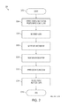
- FIG. 3 illustrates a system for transferring audio data from a domain of a source clock signal to a domain of a TBC audio clock signal, in accordance with an aspect of the present invention
- FIG. 4 illustrates an example method for the operation of the system of FIG. 3 , in accordance with an aspect of the present invention.
- FIG. 5 illustrates an example set of calculation and conversion tables used in the system of FIG. 3 , in accordance with an aspect of the present invention.
- a system and method is able to perform the process of transferring audio data from a domain of a source clock signal to a domain of a TBC audio clock signal in a simple and cost-effective manner.
- FIG. 3 illustrates a system 300 for transferring audio data from a domain of a source clock signal to a domain of a TBC audio clock signal, in accordance with an aspect of the present invention.
- System 300 includes a field programmable gate array (FPGA) 302 , double data rate synchronous dynamic random access memory (DDR 2 SDRAM) 106 , numerically controlled oscillator (NCO) 108 , video clock synthesizer 110 , audio clock synthesizer 112 and an encoder 314 .
- FPGA field programmable gate array
- DDR 2 SDRAM double data rate synchronous dynamic random access memory
- NCO numerically controlled oscillator
- FPGA 302 includes DDR 2 controller 146 , audio de-embedder 118 , FIFO buffer 120 and NCO controller 148 .
- DDR 2 106 and DDR 2 controller 146 together may be considered frame synchronizer and buffer 116 .
- NCO 108 and NCO controller 148 together may be considered TBC clock synthesizer 122 .
- audio de-embedder 118 is arranged to receive source video data 128 and to output audio data 134 .
- TBC clock synthesizer 122 is arranged to provide TBC reference clock signal 138 .
- Video clock synthesizer 110 is arranged to receive TBC reference clock signal 138 and to output TBC video clock signal 140 .
- Audio clock synthesizer 112 is arranged to receive TBC reference clock signal 138 and to output TBC audio clock signal 142 .
- FIFO buffer 120 is arranged to receive audio data 134 and source video clock signal 126 and to output TBC audio data 136 .
- Frame synchronizer and buffer 116 is arranged to receive source video clock signal 126 , source video data 128 and TBC video clock signal 140 and output TBC video data 132 .
- Encoder 314 is arranged to receive TBC video data 132 , TBC audio data 136 , TBC video clock signal 140 and TBC audio clock signal 142 .
- Audio de-embedder 118 is operable to strip out the portions of audio data from source video data 128 and provide portions to FIFO buffer 120 as audio data 134 . Audio data 134 is written into FIFO buffer 120 with source video clock signal 126 . Unlike conventional system 100 discussed above with reference to FIG. 1 , in system 300 , audio data 136 is read from buffer 120 with TBC Audio Clock 142 .
- system 300 does not contain a clock synthesizer to derive a source audio clock signal from source video clock signal 126 (such as source audio clock synthesizer 102 in conventional system 100 ). Rather, TBC audio clock signal 142 is instead supplied to FIFO buffer 120 as the read clock signal such that resulting output (TBC audio data 136 ) is in the domain of TBC audio clock signal 142 . Further, encoder 314 does not contain an audio buffer (such as audio buffer 124 in conventional system 100 ), nor does encoder 314 exchange frame sync status with frame synchronizer and buffer 116 .
- TBC video clock signal 140 and TBC audio clock signal 142 are generated from a single source, TBC reference clock signal 138 . Accordingly TBC video data 132 will always be read from frame synchronizer and buffer 116 with in a manner corresponding to audio data 136 being read from FIFO buffer 120 .
- process 400 starts (S 202 ).
- Source video data 128 for encoding is supplied to the video and audio buffers.
- Audio de-embedder 118 receives source video data 128 , which includes video data portions and audio data portions, and extracts the audio data portions as audio data 134 (S 206 ). Audio de-embedder 118 then provides audio data 134 to FIFO buffer 120 . Source video data 128 is concurrently provided to frame synchronizer and buffer 116 .
- Source video data 128 is then written to the video and audio buffers (S 208 ).
- Source video clock signal 126 enables source video data 128 to be written into frame synchronizer and buffer 116 and additionally enables audio data 134 to be written into FIFO buffer 120 .
- TBC video data 132 and audio data 136 are then supplied to encoder 314 (S 402 ).
- TBC video data 132 is read from frame synchronizer and buffer 116 using TBC video clock signal 140 .
- TBC video data 132 is then provided to encoder 314 .
- Audio data 136 is read from FIFO buffer 120 using TBC audio clock signal 142 . Audio data 136 is then provided to encoder 314 .
- TBC video clock signal 140 writes TBC video data 132 into encoder 314 while TBC audio clock signal 142 writes audio data 136 into encoder 314 (S 404 ).
- Encoder 314 then encodes TBC video data 132 and audio data 136 (S 214 ) in accordance with a predetermined coding scheme and process 200 stops (S 216 ).
- Method 400 differs from method 200 discussed above in that, process 400 does not derive a source audio clock signal from the source video clock signal and does not buffer audio data and then transfer the audio data to the domain of the TBC audio clock signal. This is because in step S 402 , audio data 134 is transferred from the domain of source video clock signal 126 to that of TBC audio clock signal 142 , avoiding the generation of a source audio clock signal and also the need for encoder 314 to buffer audio data 136 to complete its clock domain transfer.
- TBC reference clock signal 138 output from TBC clock synthesizer 122 is a 27 MHz signal.
- TBC reference clock signal 138 is supplied to two devices; TBC video clock synthesizer 110 and TBC audio clock synthesizer 112 .
- TBC video clock synthesizer 110 is used to generate the required video frequency (TBC video clock signal 140 ), which may include frequencies such as 27 MHz, 74.25 MHz, or 74.25*1000/1001 MHz, depending on the video format.
- TBC audio clock synthesizer 112 is used to generate the required audio frequency (TBC audio clock signal 142 ), which may be a multiple of 32 kHz, 44.1 kHz, or 48 kHz, depending on the audio sampling rate. It should be noted that the generation of an audio frequency from a 27 MHz clock signal (TBC reference clock signal 138 ) can be easily achieved with readily available and inexpensive parts. In contrast, the generation of an audio frequency using an HD video clock signal (as done in conventional system 100 , in S 204 of process 200 ) requires costly and hard-to-obtain devices. Source audio clock synthesizer 102 is typically a very expensive and difficult-to-find clock synthesis device.
- frame synchronizer and buffer 116 is used to transfer source video data 128 from the domain of source video clock signal 126 to the domain of TBC video clock signal 140 (S 410 of process 400 ).
- a “depth” of a frame buffer is considered the register size of the frame buffer, wherein each register is operable to store image data corresponding to a single frame.
- a frame buffer having a depth of one (1) may store image data corresponding to a single frame
- a frame buffer having a depth of five (5) may store image data corresponding to five frames.
- the minimum depth of the video frame buffer in frame synchronizer and buffer 116 is 2 video frames, and during operation, the level may vary by anywhere between 1 and 2 frames.
- TBC video clock signal 140 can be adjusted until the depth returns to the initial value.
- embedded audio data is extracted from source video data 128 and written to FIFO buffer 120 in the domain of source video clock signal 126 .
- the audio data is written to FIFO buffer 120 in the domain of source audio clock signal 130 .
- the audio data is read from FIFO buffer 120 in the domain of TBC audio clock signal 142 . In this manner, audio data is transferred from either the domain of source video clock signal 126 (in the case of embedded audio) or the domain of source audio clock signal 130 (external audio) to the domain of TBC audio clock signal 142 .
- FIFO buffer 120 For this clock domain transfer of audio data, as long as the “write” clock signal (source video clock signal 126 , in the case of embedded audio) and the “read” clock signal (TBC audio clock signal 142 ) of FIFO buffer 120 are locked, there will be no problems. However, if TBC clock synthesizer 122 is unable to lock or loses lock momentarily or periodically, FIFO buffer 120 may underflow or overflow.
- FIFO buffer 120 can help make the overflows/underflows less frequent, but will not eliminate them. Further, as mentioned earlier, increasing the depth of FIFO buffer 120 may introduce AV synchronization delays. Thus, in accordance with an aspect of the present invention, in system 300 this problem is solved by reproducing the behavior of frame synchronization and buffer 116 in FIFO buffer 120 when the source video clock signal 126 and TBC video clock signal 140 are not locked. This can be accomplished by creating FIFO buffer 120 deep enough to hold at least one video frame worth of audio data and then initializing FIFO buffer 120 to the same depth as the video frame buffer in frame synchronization and buffer 116 .
- FIFO buffer 120 since FIFO buffer 120 is being read with an audio clock signal that is derived from TBC reference clock signal 138 , any manipulation of TBC reference clock signal 138 to maintain the level of the video frame buffer (as discussed previously) will be reflected in FIFO buffer 120 as well, and therefore FIFO buffer 120 will track the video frame buffer's depth at all times. Thus, as long as video frame buffer level does not empty or fill up, FIFO buffer 120 will not overflow or underflow. An example implementation of this aspect of the present invention will now be discussed in further detail with reference to FIG. 5 .
- FIG. 5 illustrates an example set of calculation and conversion tables 500 used in system 300 , in accordance with an aspect of the present invention.
- Table set 500 includes table 502 and table 504 .
- Table 502 includes columns 506 , 508 , 510 and 512 , whereas table 504 includes columns 514 and 516 .
- Table 502 illustrates calculations of audio samples per video lines for a variety of video formats.
- Table 504 illustrates a lookup table that may be maintained in FPGA 302 , which provides the formula for the number of audio samples, given the number of audio lines for a variety of video formats.
- tables 502 and 504 will be illustrated in the following example.
- FPGA 302 detects source video data 128 is good and begins writing video data to frame synchronizer and buffer 116 . After one complete video frame has been written, the frame synchronizing portion of frame synchronizer and buffer 116 starts waiting for a start-of-frame signal from the frame template generator to start reading from the video frame buffer portion. Suppose that this occurs 300 video lines after the first frame was written. Thus, FIFO buffer 120 must be initialized with an equivalent amount of audio data. For audio data at 48 kHz, there are 48,000 audio samples per second.
- Table 504 is then used within FPGA 302 to obtain the conversion factor, or the number of audio samples per video line.
- the video format is 1080i, so column 514 is used.
- the conversion formula in this case for the number of audio samples required would be 1.44n (where n is the number of video lines required), which may be implemented as n+n/2 ⁇ n/16 inside FPGA 302 .
- a FIFO buffer is implemented inside an FPGA that tracks the behavior of the video frame buffer, thereby allowing a glitch-free transfer of audio data from the domain of the source clock signal to a domain of the TBC clock signal, thus eliminating the need for costly clock synthesis devices that would otherwise be required for such a transfer.
- exact AV synchronization is guaranteed within the FPGA, without the need for a more complicated design involving multiple devices, such as the encoder.
- This approach can be implemented for all types of audio data, whether pre-compressed or uncompressed and embedded in video data or from an external source.
Abstract
Description
Claims (20)
Priority Applications (1)
| Application Number | Priority Date | Filing Date | Title |
|---|---|---|---|
| US12/632,177 US8855212B2 (en) | 2009-12-07 | 2009-12-07 | System and method for AV synchronization of encoder data |
Applications Claiming Priority (1)
| Application Number | Priority Date | Filing Date | Title |
|---|---|---|---|
| US12/632,177 US8855212B2 (en) | 2009-12-07 | 2009-12-07 | System and method for AV synchronization of encoder data |
Publications (2)
| Publication Number | Publication Date |
|---|---|
| US20110135010A1 US20110135010A1 (en) | 2011-06-09 |
| US8855212B2 true US8855212B2 (en) | 2014-10-07 |
Family
ID=44081989
Family Applications (1)
| Application Number | Title | Priority Date | Filing Date |
|---|---|---|---|
| US12/632,177 Active 2031-07-15 US8855212B2 (en) | 2009-12-07 | 2009-12-07 | System and method for AV synchronization of encoder data |
Country Status (1)
| Country | Link |
|---|---|
| US (1) | US8855212B2 (en) |
Families Citing this family (3)
| Publication number | Priority date | Publication date | Assignee | Title |
|---|---|---|---|---|
| CN104333677A (en) * | 2013-07-23 | 2015-02-04 | 合肥赛为智能有限公司 | Video and audio signal demultiplexing device and demultiplexing method thereof |
| JP6978852B2 (en) * | 2017-05-10 | 2021-12-08 | キヤノン株式会社 | Synchronous signal output device, control method, and program |
| CN113596549B (en) * | 2020-10-13 | 2023-09-22 | 杭州涂鸦信息技术有限公司 | Audio and video synchronization method and device based on different reference clocks and computer equipment |
Citations (3)
| Publication number | Priority date | Publication date | Assignee | Title |
|---|---|---|---|---|
| US6493357B1 (en) * | 1994-06-27 | 2002-12-10 | Sony Corporation | Digital serial data interface |
| US7474724B1 (en) * | 2004-10-13 | 2009-01-06 | Cirrus Logic, Inc. | Method and system for video-synchronous audio clock generation from an asynchronously sampled video signal |
| US20090310941A1 (en) * | 2004-05-28 | 2009-12-17 | Melanson John L | Audio clocking in video applications |
-
2009
- 2009-12-07 US US12/632,177 patent/US8855212B2/en active Active
Patent Citations (3)
| Publication number | Priority date | Publication date | Assignee | Title |
|---|---|---|---|---|
| US6493357B1 (en) * | 1994-06-27 | 2002-12-10 | Sony Corporation | Digital serial data interface |
| US20090310941A1 (en) * | 2004-05-28 | 2009-12-17 | Melanson John L | Audio clocking in video applications |
| US7474724B1 (en) * | 2004-10-13 | 2009-01-06 | Cirrus Logic, Inc. | Method and system for video-synchronous audio clock generation from an asynchronously sampled video signal |
Also Published As
| Publication number | Publication date |
|---|---|
| US20110135010A1 (en) | 2011-06-09 |
Similar Documents
| Publication | Publication Date | Title |
|---|---|---|
| EP1414235B1 (en) | Audio-video-system and method supporting a pull data flow scheme | |
| KR100296733B1 (en) | Method and system for selectively independently or simultaneously updating multiple system time clocks in an mpeg system | |
| US6429902B1 (en) | Method and apparatus for audio and video end-to-end synchronization | |
| US7852160B2 (en) | NCO based timebase recovery system and method for A/V decoder | |
| CN101419827B (en) | Method for synchronzing audio and video data in avi file | |
| US20060120462A1 (en) | Compressed stream decoding apparatus and method | |
| US6948185B1 (en) | Process and device for synchronizing an MPEG decoder | |
| US8855212B2 (en) | System and method for AV synchronization of encoder data | |
| EP1414247B1 (en) | Data rate management system and method for A/V decoder | |
| EP1414249B1 (en) | A/V decoder having a clocking scheme that is independent of input data streams | |
| JP2010506538A (en) | Clock generation using a minimum number of crystals in multimedia systems | |
| US20080124043A1 (en) | Multiplexing apparatus, multiplexing method, and computer product | |
| KR20080089721A (en) | Lip-synchronize method | |
| KR100311464B1 (en) | Apparatus for synchronizing audio/video of digital tv | |
| JP2006191538A (en) | Compressed stream decoding instrument and compressed stream decoding method | |
| JP4000771B2 (en) | Synchronization management system | |
| JP2558730B2 (en) | Video transmission system | |
| JP2003339023A (en) | Moving picture reproducing apparatus | |
| JPH0937208A (en) | Method and device for moving image expansion reproduction | |
| KR100267371B1 (en) | An interface system between the system and audio decoder of mpeg-2 | |
| JP2004023134A (en) | Device for synchronizing image with sound | |
| JP4157795B2 (en) | Video digital recording and playback device | |
| JP2016187142A (en) | Information processing method, information processing unit and moving image data transmission system | |
| JPH08280008A (en) | Method and device for encoding | |
| KR100348240B1 (en) | Pts/dts controller using numerically controlled oscillator |
Legal Events
| Date | Code | Title | Description |
|---|---|---|---|
| AS | Assignment |
Owner name: GENERAL INSTRUMENT CORPORATION, PENNSYLVANIA Free format text: ASSIGNMENT OF ASSIGNORS INTEREST;ASSIGNOR:NAJEEB, TALHA;REEL/FRAME:023613/0235 Effective date: 20091207 |
|
| AS | Assignment |
Owner name: BANK OF AMERICA, N.A., AS ADMINISTRATIVE AGENT, IL Free format text: SECURITY AGREEMENT;ASSIGNORS:ARRIS GROUP, INC.;ARRIS ENTERPRISES, INC.;ARRIS SOLUTIONS, INC.;AND OTHERS;REEL/FRAME:030498/0023 Effective date: 20130417 Owner name: BANK OF AMERICA, N.A., AS ADMINISTRATIVE AGENT, ILLINOIS Free format text: SECURITY AGREEMENT;ASSIGNORS:ARRIS GROUP, INC.;ARRIS ENTERPRISES, INC.;ARRIS SOLUTIONS, INC.;AND OTHERS;REEL/FRAME:030498/0023 Effective date: 20130417 |
|
| STCF | Information on status: patent grant |
Free format text: PATENTED CASE |
|
| AS | Assignment |
Owner name: ARRIS TECHNOLOGY, INC., GEORGIA Free format text: MERGER AND CHANGE OF NAME;ASSIGNOR:GENERAL INSTRUMENT CORPORATION;REEL/FRAME:035176/0620 Effective date: 20150101 Owner name: ARRIS TECHNOLOGY, INC., GEORGIA Free format text: MERGER AND CHANGE OF NAME;ASSIGNORS:GENERAL INSTRUMENT CORPORATION;GENERAL INSTRUMENT CORPORATION;REEL/FRAME:035176/0620 Effective date: 20150101 |
|
| AS | Assignment |
Owner name: ARRIS ENTERPRISES, INC., GEORGIA Free format text: ASSIGNMENT OF ASSIGNORS INTEREST;ASSIGNOR:ARRIS TECHNOLOGY, INC;REEL/FRAME:037328/0341 Effective date: 20151214 |
|
| MAFP | Maintenance fee payment |
Free format text: PAYMENT OF MAINTENANCE FEE, 4TH YEAR, LARGE ENTITY (ORIGINAL EVENT CODE: M1551) Year of fee payment: 4 |
|
| AS | Assignment |
Owner name: SETJAM, INC., PENNSYLVANIA Free format text: TERMINATION AND RELEASE OF SECURITY INTEREST IN PATENTS;ASSIGNOR:BANK OF AMERICA, N.A., AS ADMINISTRATIVE AGENT;REEL/FRAME:048825/0294 Effective date: 20190404 Owner name: GIC INTERNATIONAL HOLDCO LLC, PENNSYLVANIA Free format text: TERMINATION AND RELEASE OF SECURITY INTEREST IN PATENTS;ASSIGNOR:BANK OF AMERICA, N.A., AS ADMINISTRATIVE AGENT;REEL/FRAME:048825/0294 Effective date: 20190404 Owner name: SUNUP DESIGN SYSTEMS, INC., PENNSYLVANIA Free format text: TERMINATION AND RELEASE OF SECURITY INTEREST IN PATENTS;ASSIGNOR:BANK OF AMERICA, N.A., AS ADMINISTRATIVE AGENT;REEL/FRAME:048825/0294 Effective date: 20190404 Owner name: ARRIS KOREA, INC., PENNSYLVANIA Free format text: TERMINATION AND RELEASE OF SECURITY INTEREST IN PATENTS;ASSIGNOR:BANK OF AMERICA, N.A., AS ADMINISTRATIVE AGENT;REEL/FRAME:048825/0294 Effective date: 20190404 Owner name: TEXSCAN CORPORATION, PENNSYLVANIA Free format text: TERMINATION AND RELEASE OF SECURITY INTEREST IN PATENTS;ASSIGNOR:BANK OF AMERICA, N.A., AS ADMINISTRATIVE AGENT;REEL/FRAME:048825/0294 Effective date: 20190404 Owner name: IMEDIA CORPORATION, PENNSYLVANIA Free format text: TERMINATION AND RELEASE OF SECURITY INTEREST IN PATENTS;ASSIGNOR:BANK OF AMERICA, N.A., AS ADMINISTRATIVE AGENT;REEL/FRAME:048825/0294 Effective date: 20190404 Owner name: BROADBUS TECHNOLOGIES, INC., PENNSYLVANIA Free format text: TERMINATION AND RELEASE OF SECURITY INTEREST IN PATENTS;ASSIGNOR:BANK OF AMERICA, N.A., AS ADMINISTRATIVE AGENT;REEL/FRAME:048825/0294 Effective date: 20190404 Owner name: POWER GUARD, INC., PENNSYLVANIA Free format text: TERMINATION AND RELEASE OF SECURITY INTEREST IN PATENTS;ASSIGNOR:BANK OF AMERICA, N.A., AS ADMINISTRATIVE AGENT;REEL/FRAME:048825/0294 Effective date: 20190404 Owner name: MOTOROLA WIRELINE NETWORKS, INC., PENNSYLVANIA Free format text: TERMINATION AND RELEASE OF SECURITY INTEREST IN PATENTS;ASSIGNOR:BANK OF AMERICA, N.A., AS ADMINISTRATIVE AGENT;REEL/FRAME:048825/0294 Effective date: 20190404 Owner name: BIG BAND NETWORKS, INC., PENNSYLVANIA Free format text: TERMINATION AND RELEASE OF SECURITY INTEREST IN PATENTS;ASSIGNOR:BANK OF AMERICA, N.A., AS ADMINISTRATIVE AGENT;REEL/FRAME:048825/0294 Effective date: 20190404 Owner name: GENERAL INSTRUMENT CORPORATION, PENNSYLVANIA Free format text: TERMINATION AND RELEASE OF SECURITY INTEREST IN PATENTS;ASSIGNOR:BANK OF AMERICA, N.A., AS ADMINISTRATIVE AGENT;REEL/FRAME:048825/0294 Effective date: 20190404 Owner name: UCENTRIC SYSTEMS, INC., PENNSYLVANIA Free format text: TERMINATION AND RELEASE OF SECURITY INTEREST IN PATENTS;ASSIGNOR:BANK OF AMERICA, N.A., AS ADMINISTRATIVE AGENT;REEL/FRAME:048825/0294 Effective date: 20190404 Owner name: NETOPIA, INC., PENNSYLVANIA Free format text: TERMINATION AND RELEASE OF SECURITY INTEREST IN PATENTS;ASSIGNOR:BANK OF AMERICA, N.A., AS ADMINISTRATIVE AGENT;REEL/FRAME:048825/0294 Effective date: 20190404 Owner name: CCE SOFTWARE LLC, PENNSYLVANIA Free format text: TERMINATION AND RELEASE OF SECURITY INTEREST IN PATENTS;ASSIGNOR:BANK OF AMERICA, N.A., AS ADMINISTRATIVE AGENT;REEL/FRAME:048825/0294 Effective date: 20190404 Owner name: ARRIS ENTERPRISES, INC., PENNSYLVANIA Free format text: TERMINATION AND RELEASE OF SECURITY INTEREST IN PATENTS;ASSIGNOR:BANK OF AMERICA, N.A., AS ADMINISTRATIVE AGENT;REEL/FRAME:048825/0294 Effective date: 20190404 Owner name: GENERAL INSTRUMENT AUTHORIZATION SERVICES, INC., P Free format text: TERMINATION AND RELEASE OF SECURITY INTEREST IN PATENTS;ASSIGNOR:BANK OF AMERICA, N.A., AS ADMINISTRATIVE AGENT;REEL/FRAME:048825/0294 Effective date: 20190404 Owner name: ACADIA AIC, INC., PENNSYLVANIA Free format text: TERMINATION AND RELEASE OF SECURITY INTEREST IN PATENTS;ASSIGNOR:BANK OF AMERICA, N.A., AS ADMINISTRATIVE AGENT;REEL/FRAME:048825/0294 Effective date: 20190404 Owner name: AEROCAST, INC., PENNSYLVANIA Free format text: TERMINATION AND RELEASE OF SECURITY INTEREST IN PATENTS;ASSIGNOR:BANK OF AMERICA, N.A., AS ADMINISTRATIVE AGENT;REEL/FRAME:048825/0294 Effective date: 20190404 Owner name: ARRIS GROUP, INC., PENNSYLVANIA Free format text: TERMINATION AND RELEASE OF SECURITY INTEREST IN PATENTS;ASSIGNOR:BANK OF AMERICA, N.A., AS ADMINISTRATIVE AGENT;REEL/FRAME:048825/0294 Effective date: 20190404 Owner name: GIC INTERNATIONAL CAPITAL LLC, PENNSYLVANIA Free format text: TERMINATION AND RELEASE OF SECURITY INTEREST IN PATENTS;ASSIGNOR:BANK OF AMERICA, N.A., AS ADMINISTRATIVE AGENT;REEL/FRAME:048825/0294 Effective date: 20190404 Owner name: MODULUS VIDEO, INC., PENNSYLVANIA Free format text: TERMINATION AND RELEASE OF SECURITY INTEREST IN PATENTS;ASSIGNOR:BANK OF AMERICA, N.A., AS ADMINISTRATIVE AGENT;REEL/FRAME:048825/0294 Effective date: 20190404 Owner name: JERROLD DC RADIO, INC., PENNSYLVANIA Free format text: TERMINATION AND RELEASE OF SECURITY INTEREST IN PATENTS;ASSIGNOR:BANK OF AMERICA, N.A., AS ADMINISTRATIVE AGENT;REEL/FRAME:048825/0294 Effective date: 20190404 Owner name: ARRIS SOLUTIONS, INC., PENNSYLVANIA Free format text: TERMINATION AND RELEASE OF SECURITY INTEREST IN PATENTS;ASSIGNOR:BANK OF AMERICA, N.A., AS ADMINISTRATIVE AGENT;REEL/FRAME:048825/0294 Effective date: 20190404 Owner name: NEXTLEVEL SYSTEMS (PUERTO RICO), INC., PENNSYLVANI Free format text: TERMINATION AND RELEASE OF SECURITY INTEREST IN PATENTS;ASSIGNOR:BANK OF AMERICA, N.A., AS ADMINISTRATIVE AGENT;REEL/FRAME:048825/0294 Effective date: 20190404 Owner name: GENERAL INSTRUMENT INTERNATIONAL HOLDINGS, INC., P Free format text: TERMINATION AND RELEASE OF SECURITY INTEREST IN PATENTS;ASSIGNOR:BANK OF AMERICA, N.A., AS ADMINISTRATIVE AGENT;REEL/FRAME:048825/0294 Effective date: 20190404 Owner name: LEAPSTONE SYSTEMS, INC., PENNSYLVANIA Free format text: TERMINATION AND RELEASE OF SECURITY INTEREST IN PATENTS;ASSIGNOR:BANK OF AMERICA, N.A., AS ADMINISTRATIVE AGENT;REEL/FRAME:048825/0294 Effective date: 20190404 Owner name: ARRIS HOLDINGS CORP. OF ILLINOIS, INC., PENNSYLVAN Free format text: TERMINATION AND RELEASE OF SECURITY INTEREST IN PATENTS;ASSIGNOR:BANK OF AMERICA, N.A., AS ADMINISTRATIVE AGENT;REEL/FRAME:048825/0294 Effective date: 20190404 Owner name: 4HOME, INC., PENNSYLVANIA Free format text: TERMINATION AND RELEASE OF SECURITY INTEREST IN PATENTS;ASSIGNOR:BANK OF AMERICA, N.A., AS ADMINISTRATIVE AGENT;REEL/FRAME:048825/0294 Effective date: 20190404 Owner name: QUANTUM BRIDGE COMMUNICATIONS, INC., PENNSYLVANIA Free format text: TERMINATION AND RELEASE OF SECURITY INTEREST IN PATENTS;ASSIGNOR:BANK OF AMERICA, N.A., AS ADMINISTRATIVE AGENT;REEL/FRAME:048825/0294 Effective date: 20190404 Owner name: THE GI REALTY TRUST 1996, PENNSYLVANIA Free format text: TERMINATION AND RELEASE OF SECURITY INTEREST IN PATENTS;ASSIGNOR:BANK OF AMERICA, N.A., AS ADMINISTRATIVE AGENT;REEL/FRAME:048825/0294 Effective date: 20190404 Owner name: GENERAL INSTRUMENT AUTHORIZATION SERVICES, INC., PENNSYLVANIA Free format text: TERMINATION AND RELEASE OF SECURITY INTEREST IN PATENTS;ASSIGNOR:BANK OF AMERICA, N.A., AS ADMINISTRATIVE AGENT;REEL/FRAME:048825/0294 Effective date: 20190404 Owner name: GENERAL INSTRUMENT INTERNATIONAL HOLDINGS, INC., PENNSYLVANIA Free format text: TERMINATION AND RELEASE OF SECURITY INTEREST IN PATENTS;ASSIGNOR:BANK OF AMERICA, N.A., AS ADMINISTRATIVE AGENT;REEL/FRAME:048825/0294 Effective date: 20190404 Owner name: ARRIS HOLDINGS CORP. OF ILLINOIS, INC., PENNSYLVANIA Free format text: TERMINATION AND RELEASE OF SECURITY INTEREST IN PATENTS;ASSIGNOR:BANK OF AMERICA, N.A., AS ADMINISTRATIVE AGENT;REEL/FRAME:048825/0294 Effective date: 20190404 Owner name: NEXTLEVEL SYSTEMS (PUERTO RICO), INC., PENNSYLVANIA Free format text: TERMINATION AND RELEASE OF SECURITY INTEREST IN PATENTS;ASSIGNOR:BANK OF AMERICA, N.A., AS ADMINISTRATIVE AGENT;REEL/FRAME:048825/0294 Effective date: 20190404 |
|
| AS | Assignment |
Owner name: ARRIS ENTERPRISES LLC, GEORGIA Free format text: CHANGE OF NAME;ASSIGNOR:ARRIS ENTERPRISES, INC.;REEL/FRAME:049649/0062 Effective date: 20151231 |
|
| AS | Assignment |
Owner name: WILMINGTON TRUST, NATIONAL ASSOCIATION, AS COLLATE Free format text: PATENT SECURITY AGREEMENT;ASSIGNOR:ARRIS ENTERPRISES LLC;REEL/FRAME:049820/0495 Effective date: 20190404 Owner name: JPMORGAN CHASE BANK, N.A., NEW YORK Free format text: TERM LOAN SECURITY AGREEMENT;ASSIGNORS:COMMSCOPE, INC. OF NORTH CAROLINA;COMMSCOPE TECHNOLOGIES LLC;ARRIS ENTERPRISES LLC;AND OTHERS;REEL/FRAME:049905/0504 Effective date: 20190404 Owner name: JPMORGAN CHASE BANK, N.A., NEW YORK Free format text: ABL SECURITY AGREEMENT;ASSIGNORS:COMMSCOPE, INC. OF NORTH CAROLINA;COMMSCOPE TECHNOLOGIES LLC;ARRIS ENTERPRISES LLC;AND OTHERS;REEL/FRAME:049892/0396 Effective date: 20190404 Owner name: WILMINGTON TRUST, NATIONAL ASSOCIATION, AS COLLATERAL AGENT, CONNECTICUT Free format text: PATENT SECURITY AGREEMENT;ASSIGNOR:ARRIS ENTERPRISES LLC;REEL/FRAME:049820/0495 Effective date: 20190404 |
|
| AS | Assignment |
Owner name: WILMINGTON TRUST, DELAWARE Free format text: SECURITY INTEREST;ASSIGNORS:ARRIS SOLUTIONS, INC.;ARRIS ENTERPRISES LLC;COMMSCOPE TECHNOLOGIES LLC;AND OTHERS;REEL/FRAME:060752/0001 Effective date: 20211115 |
|
| MAFP | Maintenance fee payment |
Free format text: PAYMENT OF MAINTENANCE FEE, 8TH YEAR, LARGE ENTITY (ORIGINAL EVENT CODE: M1552); ENTITY STATUS OF PATENT OWNER: LARGE ENTITY Year of fee payment: 8 |
|
| AS | Assignment |
Owner name: ARRIS ENTERPRISES, INC., GEORGIA Free format text: ASSIGNMENT OF ASSIGNORS INTEREST;ASSIGNOR:ARRIS TECHNOLOGY, INC.;REEL/FRAME:060791/0583 Effective date: 20151214 |