US8855155B2 - Semiconductor laser light source - Google Patents
Semiconductor laser light source Download PDFInfo
- Publication number
- US8855155B2 US8855155B2 US13/579,209 US201113579209A US8855155B2 US 8855155 B2 US8855155 B2 US 8855155B2 US 201113579209 A US201113579209 A US 201113579209A US 8855155 B2 US8855155 B2 US 8855155B2
- Authority
- US
- United States
- Prior art keywords
- semiconductor
- semiconductor lasers
- optical component
- light source
- laser light
- Prior art date
- Legal status (The legal status is an assumption and is not a legal conclusion. Google has not performed a legal analysis and makes no representation as to the accuracy of the status listed.)
- Active, expires
Links
Images




Classifications
-
- H01S5/02288—
-
- G—PHYSICS
- G02—OPTICS
- G02B—OPTICAL ELEMENTS, SYSTEMS OR APPARATUS
- G02B27/00—Optical systems or apparatus not provided for by any of the groups G02B1/00 - G02B26/00, G02B30/00
- G02B27/10—Beam splitting or combining systems
-
- H—ELECTRICITY
- H01—ELECTRIC ELEMENTS
- H01S—DEVICES USING THE PROCESS OF LIGHT AMPLIFICATION BY STIMULATED EMISSION OF RADIATION [LASER] TO AMPLIFY OR GENERATE LIGHT; DEVICES USING STIMULATED EMISSION OF ELECTROMAGNETIC RADIATION IN WAVE RANGES OTHER THAN OPTICAL
- H01S5/00—Semiconductor lasers
- H01S5/02—Structural details or components not essential to laser action
- H01S5/022—Mountings; Housings
- H01S5/0225—Out-coupling of light
- H01S5/02253—Out-coupling of light using lenses
-
- H—ELECTRICITY
- H01—ELECTRIC ELEMENTS
- H01S—DEVICES USING THE PROCESS OF LIGHT AMPLIFICATION BY STIMULATED EMISSION OF RADIATION [LASER] TO AMPLIFY OR GENERATE LIGHT; DEVICES USING STIMULATED EMISSION OF ELECTROMAGNETIC RADIATION IN WAVE RANGES OTHER THAN OPTICAL
- H01S5/00—Semiconductor lasers
- H01S5/40—Arrangement of two or more semiconductor lasers, not provided for in groups H01S5/02 - H01S5/30
- H01S5/4012—Beam combining, e.g. by the use of fibres, gratings, polarisers, prisms
-
- H—ELECTRICITY
- H04—ELECTRIC COMMUNICATION TECHNIQUE
- H04N—PICTORIAL COMMUNICATION, e.g. TELEVISION
- H04N9/00—Details of colour television systems
- H04N9/12—Picture reproducers
- H04N9/31—Projection devices for colour picture display, e.g. using electronic spatial light modulators [ESLM]
- H04N9/3141—Constructional details thereof
- H04N9/315—Modulator illumination systems
- H04N9/3161—Modulator illumination systems using laser light sources
-
- G—PHYSICS
- G02—OPTICS
- G02B—OPTICAL ELEMENTS, SYSTEMS OR APPARATUS
- G02B26/00—Optical devices or arrangements for the control of light using movable or deformable optical elements
- G02B26/08—Optical devices or arrangements for the control of light using movable or deformable optical elements for controlling the direction of light
- G02B26/0816—Optical devices or arrangements for the control of light using movable or deformable optical elements for controlling the direction of light by means of one or more reflecting elements
- G02B26/0833—Optical devices or arrangements for the control of light using movable or deformable optical elements for controlling the direction of light by means of one or more reflecting elements the reflecting element being a micromechanical device, e.g. a MEMS mirror, DMD
-
- G—PHYSICS
- G02—OPTICS
- G02B—OPTICAL ELEMENTS, SYSTEMS OR APPARATUS
- G02B6/00—Light guides; Structural details of arrangements comprising light guides and other optical elements, e.g. couplings
- G02B6/24—Coupling light guides
- G02B6/42—Coupling light guides with opto-electronic elements
- G02B6/4201—Packages, e.g. shape, construction, internal or external details
- G02B6/4204—Packages, e.g. shape, construction, internal or external details the coupling comprising intermediate optical elements, e.g. lenses, holograms
- G02B6/4214—Packages, e.g. shape, construction, internal or external details the coupling comprising intermediate optical elements, e.g. lenses, holograms the intermediate optical element having redirecting reflective means, e.g. mirrors, prisms for deflecting the radiation from horizontal to down- or upward direction toward a device
-
- H—ELECTRICITY
- H01—ELECTRIC ELEMENTS
- H01S—DEVICES USING THE PROCESS OF LIGHT AMPLIFICATION BY STIMULATED EMISSION OF RADIATION [LASER] TO AMPLIFY OR GENERATE LIGHT; DEVICES USING STIMULATED EMISSION OF ELECTROMAGNETIC RADIATION IN WAVE RANGES OTHER THAN OPTICAL
- H01S5/00—Semiconductor lasers
- H01S5/005—Optical components external to the laser cavity, specially adapted therefor, e.g. for homogenisation or merging of the beams or for manipulating laser pulses, e.g. pulse shaping
- H01S5/0071—Optical components external to the laser cavity, specially adapted therefor, e.g. for homogenisation or merging of the beams or for manipulating laser pulses, e.g. pulse shaping for beam steering, e.g. using a mirror outside the cavity to change the beam direction
-
- H—ELECTRICITY
- H01—ELECTRIC ELEMENTS
- H01S—DEVICES USING THE PROCESS OF LIGHT AMPLIFICATION BY STIMULATED EMISSION OF RADIATION [LASER] TO AMPLIFY OR GENERATE LIGHT; DEVICES USING STIMULATED EMISSION OF ELECTROMAGNETIC RADIATION IN WAVE RANGES OTHER THAN OPTICAL
- H01S5/00—Semiconductor lasers
- H01S5/02—Structural details or components not essential to laser action
- H01S5/022—Mountings; Housings
- H01S5/02208—Mountings; Housings characterised by the shape of the housings
- H01S5/02212—Can-type, e.g. TO-CAN housings with emission along or parallel to symmetry axis
-
- H—ELECTRICITY
- H01—ELECTRIC ELEMENTS
- H01S—DEVICES USING THE PROCESS OF LIGHT AMPLIFICATION BY STIMULATED EMISSION OF RADIATION [LASER] TO AMPLIFY OR GENERATE LIGHT; DEVICES USING STIMULATED EMISSION OF ELECTROMAGNETIC RADIATION IN WAVE RANGES OTHER THAN OPTICAL
- H01S5/00—Semiconductor lasers
- H01S5/02—Structural details or components not essential to laser action
- H01S5/022—Mountings; Housings
- H01S5/0225—Out-coupling of light
- H01S5/02255—Out-coupling of light using beam deflecting elements
-
- H01S5/02292—
-
- H—ELECTRICITY
- H01—ELECTRIC ELEMENTS
- H01S—DEVICES USING THE PROCESS OF LIGHT AMPLIFICATION BY STIMULATED EMISSION OF RADIATION [LASER] TO AMPLIFY OR GENERATE LIGHT; DEVICES USING STIMULATED EMISSION OF ELECTROMAGNETIC RADIATION IN WAVE RANGES OTHER THAN OPTICAL
- H01S5/00—Semiconductor lasers
- H01S5/06—Arrangements for controlling the laser output parameters, e.g. by operating on the active medium
- H01S5/068—Stabilisation of laser output parameters
- H01S5/0683—Stabilisation of laser output parameters by monitoring the optical output parameters
-
- H—ELECTRICITY
- H01—ELECTRIC ELEMENTS
- H01S—DEVICES USING THE PROCESS OF LIGHT AMPLIFICATION BY STIMULATED EMISSION OF RADIATION [LASER] TO AMPLIFY OR GENERATE LIGHT; DEVICES USING STIMULATED EMISSION OF ELECTROMAGNETIC RADIATION IN WAVE RANGES OTHER THAN OPTICAL
- H01S5/00—Semiconductor lasers
- H01S5/40—Arrangement of two or more semiconductor lasers, not provided for in groups H01S5/02 - H01S5/30
- H01S5/4025—Array arrangements, e.g. constituted by discrete laser diodes or laser bar
- H01S5/4087—Array arrangements, e.g. constituted by discrete laser diodes or laser bar emitting more than one wavelength
-
- H—ELECTRICITY
- H01—ELECTRIC ELEMENTS
- H01S—DEVICES USING THE PROCESS OF LIGHT AMPLIFICATION BY STIMULATED EMISSION OF RADIATION [LASER] TO AMPLIFY OR GENERATE LIGHT; DEVICES USING STIMULATED EMISSION OF ELECTROMAGNETIC RADIATION IN WAVE RANGES OTHER THAN OPTICAL
- H01S5/00—Semiconductor lasers
- H01S5/40—Arrangement of two or more semiconductor lasers, not provided for in groups H01S5/02 - H01S5/30
- H01S5/4025—Array arrangements, e.g. constituted by discrete laser diodes or laser bar
- H01S5/4087—Array arrangements, e.g. constituted by discrete laser diodes or laser bar emitting more than one wavelength
- H01S5/4093—Red, green and blue [RGB] generated directly by laser action or by a combination of laser action with nonlinear frequency conversion
Definitions
- the present invention relates to a semiconductor laser light source.
- German Patent Publication DE 10 2007 062 047 A1 discloses a compact housing.
- One aspect of the invention provides a semiconductor laser light source of small geometric dimensions.
- the latter comprises a carrier with a carrier top.
- the carrier takes the form for example of a metal core printed circuit board or a printed circuit board.
- the carrier preferably exhibits an average specific thermal conductivity of at least 80 W/mK.
- the semiconductor laser light source comprises a semiconductor laser emitting in the red spectral range, a semiconductor laser emitting in the green spectral range and a semiconductor laser emitting in the blue spectral range.
- the semiconductor laser light source thus contains at least three semiconductor lasers emitting in particular directly in the corresponding spectral ranges.
- an optical component is arranged downstream of at least one of the semiconductor lasers, preferably all the semiconductor lasers together, in a direction of emission.
- the optical component it is in particular possible for partial beams emitted by each of the for example three semiconductor lasers of the semiconductor laser light source to be combined into a whole beam, i.e., beam combination may preferably be achieved by means of the optical component.
- Whole beam means in particular that all cross-sections of the partial beams overlap and that the partial beams extend in the same direction.
- the same direction means preferably that paired overlap of the cross-sections of the partial beams from the semiconductor laser light source as far as for example to a projection surface amounts to at least 50% or at least 75%.
- the latter comprises a cover.
- the cover and the carrier substantially define an enclosure.
- the enclosure is sealed tightly, in particular gas-tightly. Tightly means that over the service life of the semiconductor laser light source no or no significant gas exchange takes place between the interior of the enclosure and a region outside the enclosure. Tightness for the purposes of the present application may be achieved in particular in that the cover is connected by way of a metal solder, by way of a glass solder or by way of a weld seam to the carrier or to a housing frame.
- the enclosure is preferably evacuated or is filled with a noble gas, with nitrogen or with dried air.
- the at least one semiconductor laser particularly preferably all the semiconductor lasers, and the optical component are located in the enclosure and are jointly housed.
- the above-stated components are in the immediate spatial vicinity of one another and are preferably not separated from one another by barriers of solid materials.
- the dimensions of the enclosure amount to at most 8 mm ⁇ 8 mm ⁇ 7 mm, in particular at most 5 mm ⁇ 5 mm ⁇ 4 mm, preferably at most 3 mm ⁇ 3 mm ⁇ 4 mm, particularly preferably at most 2.5 mm ⁇ 2.5 mm ⁇ 3 mm.
- the smallest value here indicates in particular the height above the carrier top.
- the enclosure may be completely surrounded by a cuboid of the stated dimensions.
- the size of the enclosure amounts at most to 400 mm 3 , in particular at most to 100 mm 3 , preferably at most to 30 mm 3 , particularly preferably at most to 12 mm 3 .
- the base area of the enclosure on the carrier top alternatively or additionally measures at most 60 mm 2 , in particular at most 25 mm 2 , preferably at most 10 mm 2 , particularly preferably at most 6 mm 2 .
- the semiconductor laser light source comprises a carrier with a carrier top and at least two semiconductor lasers, in particular in each case at least one semiconductor laser emitting in the red, at least one in the green and at least one in the blue spectral range.
- the semiconductor lasers are mounted on the carrier top.
- the semiconductor laser light source furthermore comprises at least one optical component, which is arranged downstream of at least one, preferably all of the semiconductor lasers in a direction of emission.
- the semiconductor lasers and the optical component are housed tightly in a common enclosure by way of a cover. The dimensions of the enclosure, viewed in three orthogonal spatial directions, amount in each case to at most 8 mm ⁇ 8 mm ⁇ 7 mm.
- a particularly compact semiconductor laser light source may be achieved by mounting the semiconductor laser and the optical component jointly in the enclosure.
- the compactness of the semiconductor laser light source may be additionally increased by various combinations of further measures. Such measures are in particular the design of the semiconductor lasers, the arrangement and development of the optical component and guidance of electrical supply lines on the carrier and the manner of contacting the semiconductor lasers.
- an imaging unit and safety devices may likewise be mounted compactly at least indirectly on the carrier or on the enclosure.
- the semiconductor laser light source may be used for example as a projection unit in compact, portable equipment such as mobile telephones or small computers.
- the semiconductor laser light source may be used in particular to generate polychromatic light, preferably white light.
- the optical component is arranged jointly and optically directly downstream of the semiconductor lasers.
- Optically directly downstream means that no further optically active components are located between a radiation exit face of the respective semiconductor laser and a radiation entrance face of the optical component.
- no lens in particular no “fast-axis collimating lens” is mounted between the semiconductor laser and the optical component in a beam path of the partial beams emitted in each case by the semiconductor lasers. Due to the only small distance between the optical component and the semiconductor lasers, it is possible to dispense with additional lenses in addition to the optical component inside the enclosure. In this way, the compactness of the semiconductor laser light source may be increased and a particularly small enclosure achieved.
- the optical component is not designed to reduce the divergence of partial beams, which are emitted by the semiconductor lasers, or the divergence of a whole beam, which is formed by the superimposed partial beams.
- the optical component does not serve to focus the radiation, but instead preferably solely to combine the partial beams into the whole beam.
- the optical component comprises for example solely planar shaped radiation entrance faces and radiation exit faces.
- a lens which is in particular not rotationally symmetrical in shape or an optical system comprising a plurality of lenses is arranged downstream of the optical component.
- the lens may be mounted directly on the optical component, for example via a bonding agent or welding.
- the optical component is mounted outside the enclosure, for example on the cover.
- the lens or the optical system is in particular designed to reduce the divergence of the whole beam.
- the ellipticity of the beam cross-section of the whole beam is preferably less than 4, in particular less than 2, depending on the lens or the optical system.
- the lens or the optical system is designed to generate a linear beam cross-section of the whole beam.
- the ellipticity of the beam cross-section then amounts in particular to at least 10 or at least 20.
- the semiconductor laser light source may then be used in a scanner or in a scanning unit.
- the semiconductor laser light source comprises at least two semiconductor lasers, which emit radiation of the same wavelength.
- the semiconductor laser light source comprises a laser bar with a plurality of semiconductor lasers, which emit radiation at the same wavelength.
- the semiconductor laser light source at least two of the partial beams emitted by the semiconductor lasers are differently polarized.
- the optical component is then preferably a polarization-selective element, such that combining partial beams in particular of the same wavelength may proceed by exploiting the different polarizations of the partial beams.
- the cover comprises a light exit disc, which is oriented obliquely to the carrier.
- An angle ⁇ between the carrier and the light exit disc is preferably between 45° and 85° inclusive.
- the semiconductor laser light source is mechanically and/or electrically surface-mountable and/or surface-contactable.
- the semiconductor laser light source may be attached by soldering to a mounting support by way of a carrier bottom remote from the carrier top.
- the semiconductor laser light source is connected mechanically and preferably thermally to the mounting support. If the carrier bottom is patterned and electrical conductor tracks are located on the carrier bottom, electrical contacting of the semiconductor laser light source may also take place at the same time as the mechanical and thermal connection.
- the semiconductor laser light source is contacted in particular without a bonding wire. By economising on bonding wires, the space requirement of the semiconductor laser light source may be reduced and a particularly small enclosure and low structural height may be achieved.
- one or all of the semiconductor lasers are electrically and mechanically contacted without bonding wires in the enclosure with in each case at least two electrical conductor tracks on the carrier top.
- Contact points for bonding wires typically have a comparatively large space requirement of around 2500 ⁇ m 2 .
- the bending radii needed by bonding wires also makes a minimum component height necessary, which is markedly greater than the structural height of the semiconductor lasers themselves. Because the semiconductor lasers are contacted without bonding wires, the semiconductor laser light source may be of more compact construction and a particularly small enclosure may be achieved.
- the electrical conductor tracks are connected on the carrier top by way of vias to electrical conductor tracks on the carrier bottom.
- the carrier bottom is then designed for surface mounting of the semiconductor laser light source.
- Such conductor tracks allow space-saving construction of the semiconductor laser light source.
- an imaging optical system are mounted on the carrier top of the carrier or on the top of an intermediate carrier on which the carrier is mounted.
- the imaging optical system comprise for example a micro-electromechanical mirror, or MEMS mirror for short, or a diffractive optical element, or DOE for short.
- a DOE comprises an optical diffraction grating and is designed in particular to produce an image which does not vary over time, for example a logo.
- the semiconductor laser source comprises at least one proximity sensor.
- the proximity sensor is mounted space-savingly on the carrier top of the carrier or on the top of the intermediate carrier and is designed to detect objects in the image field of the semiconductor laser light source.
- the semiconductor laser light source includes safety control electronics. These are designed to reduce the output power of the semiconductor lasers as a function of a signal from the proximity sensor. With high maximum semiconductor laser output powers in particular, there is a risk of damage to the eyes of people in the image field. The risk of eye damage may be reduced by the proximity sensor in cooperation with the safety control electronics.
- the semiconductor lasers are each designed to generate a luminous flux of at least 8 lm, in particular of at least 12 lm.
- the semiconductor laser light source is designed to emit a luminous flux of at least 25 lm or at least 40 lm in total.
- Such high luminous fluxes may be produced by the compact structure of the semiconductor laser light source and by low thermal resistances.
- the semiconductor laser light source comprises at least one monitor diode, which is designed to detect radiation emitted by the semiconductor lasers.
- the monitor diode enables active power readjustment of the semiconductor lasers, in particular colour correction of an emitted overall radiation.
- the semiconductor laser light source comprises precisely one monitor diode, which is mounted indirectly or directly on the optical component.
- the precisely one monitor diode allows detection of a fraction of the radiation from each of the partial beams emitted by the semiconductor lasers. In other words, fractions of the radiation emitted by the semiconductor lasers are in each case guided through the optical component to the one monitor diode.
- Just one monitor diode allows economies of components and results in a more compact semiconductor laser light source and a particularly small enclosure.
- At least one of the semiconductor lasers comprises a semiconductor body, which comprises top face metallization on a major face remote from the carrier top.
- the top face metallization preferably extends at least 50% or at least 75% of the way along a longitudinal direction of the semiconductor body.
- the top face metallization allows current to be supplied to the semiconductor body. In this way, it is possible to dispense with additional electrical contact points on the semiconductor bodies, whereby said bodies can be of more compact structure and whereby a particularly small enclosure may be achieved.
- the top face metallization is connected conductively via a side face metallization, which is applied at least in places on a longitudinal side of the semiconductor body, to an electrical conductor track on the carrier top of the carrier.
- a side face metallization which is applied at least in places on a longitudinal side of the semiconductor body, to an electrical conductor track on the carrier top of the carrier.
- openings may be created through the semiconductor body which are filled at least partially with an electrically conductive material and connect the top face metallization electrically conductively to a conductor track on the carrier top.
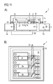
- FIGS. 1 to 3 , 7 to 16 , 18 and 19 are schematic representations of exemplary embodiments of semiconductor laser light sources described herein;
- FIGS. 4 and 17 are schematic representations of modifications of semiconductor laser light sources
- FIGS. 5 to 6 are schematic representations of exemplary embodiments of semiconductor lasers described herein.
- FIG. 20 is a schematic representation of an exemplary embodiment of a cover for semiconductor laser light sources described herein.
- FIG. 1A is a schematic sectional representation and FIG. 1B is a schematic plan view of an exemplary embodiment of a semiconductor laser light source 1 .
- the semiconductor laser light source 1 comprises a carrier 2 with a carrier top 20 and a carrier bottom 25 opposite thereto. Electrical conductor tracks 6 a , 6 b are formed on the carrier top 20 by metallization. Three semiconductor lasers 3 are mounted on in each case two of the conductor tracks 6 a , 6 b via a bonding agent 21 . In the plan view according to FIG. 1B , the semiconductor lasers 3 are merely indicated by broken lines. The semiconductor lasers 3 each overlap partially with the conductor tracks 6 a , 6 b on the carrier top 25 , see FIG. 1B .
- the semiconductor lasers 3 may be driven electrically separately and mutually independently. External electrical contacting of the semiconductor laser light source 1 proceeds via bonding wires 19 .
- the bonding wires 19 are mounted outside the enclosure 10 on the conductor tracks 6 a , 6 b.
- Metallization 7 is additionally applied to the carrier bottom 25 , which metallization preferably extends over the entirety or over the majority of the carrier bottom 25 and via which the carrier 2 may be connected to an external mounting support, not shown, by way of soldering or by way of adhesive bonding.
- the carrier 2 preferably further exhibits high specific thermal conductivity, such that the thermal resistance between the semiconductor lasers 3 and the mounting support, not shown, is low.
- a housing frame 18 is optionally mounted on the carrier top 20 via the conductor tracks 6 a , 6 b .
- a cover 5 is attached by way of a sealant 17 to the housing frame 18 , which is made for example of metal or glass or with a semiconductor material such as silicon or with a plastics material.
- the cover 5 is transparent to the radiation generated by the semiconductor lasers 3 .
- the sealant 17 may be a metal solder, a glass solder or a weld seam.
- An electrically insulating layer not shown in the figures is mounted between the conductor tracks 6 a , 6 b and the housing frame 18 . If no housing frame 18 is present, the cover 5 is preferably mounted directly on the carrier top 20 and the conductor tracks 6 a , 6 b or on the electrically insulating layer, unlike in the drawing.
- An enclosure 10 is surrounded in gas-tight manner by the carrier 2 , the housing frame 18 and the cover 5 .
- the enclosure 10 is filled with dried air or with nitrogen, for example.
- the semiconductor lasers 3 are located jointly together with an optical component 4 a , 4 b in the enclosure 10 .
- the cover 5 and the optical component 4 a , 4 b and the micro-electromechanical mirror 11 are not shown in FIG. 1B to simplify the illustration.
- the optical component 4 a , 4 b is attached to the cover 5 . Focusing of radiation emitted by the semiconductor lasers 3 may be achieved by way of part of the optical component 4 a . Beam deflection and beam combination of partial beams into a whole beam Q proceed via part of the optical component 4 b . The whole beam Q is guided to an imaging unit, embodied by a micro-electromechanical mirror 11 .
- the micro-electromechanical mirror 11 generates a time-variable image 9 , such that the semiconductor laser light source 1 may be used as a projector.
- the image 9 is preferably generated by way of row scanning or column scanning of an image area or via Lissajous figures. It is likewise possible for the semiconductor laser light source 1 to be used as a pointing device, for instance as a laser pointer.
- the base area of the enclosure 10 on the carrier top 20 has dimensions of at most 2.5 mm ⁇ 2.5 mm.
- the height of the enclosure 10 in a direction perpendicular to the carrier top 20 , amounts to at most 1.5 mm.
- the external dimensions of the housing frame 18 and the cover 5 exceed the internal dimensions of the enclosure 10 preferably by at most 40%, in particular at most 25%.
- the electrical power consumption of the semiconductor lasers 3 amounts in total for example to at least 1 W or at least 2 W.
- the semiconductor laser light source 1 may preferably be assembled or mounted in the panel or at wafer level, in particular using a “full wafer” process.
- FIG. 2 illustrates a further exemplary embodiment of the semiconductor laser light source 1 .
- the conductor tracks 6 a , 6 b on the carrier top 20 are connected to corresponding electrical conductor tracks 7 a , 7 b on the carrier bottom 25 by way of electrical vias 67 a , 67 b .
- the vias 67 a , 67 b are located next the cover 5 , when the carrier top 20 is seen in plan view.
- the conductor tracks 7 a , 7 b on the carrier bottom 25 see the view from below according to FIG. 2B , resemble straight lines and extend, when viewed in a longitudinal direction, preferably over the entire carrier bottom 25 , in order to ensure high thermal contact with a mounting support, not shown, in the event of surface mounting.
- the area of the total carrier bottom 25 occupied by the conductor tracks 7 a , 7 b amounts for example to more than 50% or more than 75%.
- the semiconductor lasers 3 may be individually drivable but rather partially or completely to be connected electrically in parallel or in series.
- Corresponding circuit configurations may be produced by arrangement of the conductor tracks 6 a , 6 b on the carrier top 20 and of the conductor tracks 7 a , 7 b on the carrier bottom 25 .
- the optical component 4 is mounted directly on the cover 5 .
- the imaging optical system is formed by a diffractive optical element 12 .
- the diffractive optical element 12 comprises a diffraction grating and is designed to display an image of invariable shape over time, for example in the form of a company logo. However, the color of the image may be variable over time, by supplying current to the semiconductor laser 3 in a time-variable manner.
- beam deflection and beam combining is effected by the optical component 4 , which is formed directly on the cover 5 .
- a lens 8 is mounted for beam-focusing on the cover 5 outside the enclosure 10 .
- the lens 8 and/or the optical component 4 may be in one-piece with the cover 5 , as indeed in the other exemplary embodiments.
- FIG. 4 shows a modification of a light source 1 ′, in which just one semiconductor laser 3 is located in the enclosure 10 .
- the enclosure 10 may then be made smaller and is for example at most 5 mm 3 or at most 2.5 mm 3 in size.
- the conductor tracks 6 a , 6 b and further optionally present components of the light source 1 ′ are preferably configured in a manner similar to the illustrated exemplary embodiments of the semiconductor laser light source 1 .
- Features of the semiconductor laser light source 1 are therefore also disclosed for the light source 1 ′ and vice versa.
- FIGS. 5 and 6 are perspective illustrations of preferred embodiments of the semiconductor lasers 3 r , 3 g , 3 b .
- the semiconductor lasers 3 r , 3 g , 3 b each comprise a substrate 33 , which is formed for example with a ceramic or consists of a ceramic.
- Two electrical conductor tracks 34 n , 34 p are formed by metallization on each of the substrates 33 .
- Each of the semiconductor bodies 30 of the semiconductor lasers 3 r , 3 g , 3 b is mounted on its own separate substrate 33 .
- a semiconductor body 30 is contacted electrically in each case via the conductor tracks 34 n on a side facing the substrate 33 , for example by means of a solder, for instance an AuSn solder.
- the partial beams T 1 , T 2 , T 3 emitted by the semiconductor lasers 3 r , 3 g , 3 b are indicated by arrows.
- top face metallization 32 is applied, which covers the majority of the major faces of the semiconductor bodies 30 remote from the substrates 33 .
- Side face metallization 35 is applied to longitudinal sides of the semiconductor bodies 30 , by means of which the top face metallization 32 is connected to the conductor tracks 34 p .
- electrically insulating interlayers which are not shown are formed between the semiconductor bodies 30 and the side face metallization 35 .
- openings 31 are formed through the semiconductor bodies 30 , the openings 31 being surrounded by semiconductor material of the semiconductor body 30 and filled at least in part with an electrically conductive material. Between this electrically conductive material and the semiconductor material, an electrically insulating interlayer, not shown in FIG. 6 , is preferably located in the openings 31 .
- the at least partially filled openings 31 provide an electrical connection from the conductor track 34 p to the top face metallization 32 .
- a plurality of recesses 36 are formed on longitudinal sides of the semiconductor body 30 .
- a predetermined breaking point may be formed by these recesses 36 along the longitudinal side, along which predetermined breaking point the semiconductor bodies 30 are singulated.
- the side face metallization 35 which connects the top face metallization 32 electrically with the conductor tracks 34 p , is applied in particular solely in the recesses 36 .
- the conductor tracks 34 n , 34 p are preferably connected electrically conductively with electrical terminal areas, not shown in FIGS. 5 and 6 , on a bottom of the substrates 33 remote from the semiconductor bodies 30 , such that the semiconductor lasers 3 r , 3 g , 3 b may be mounted on the carrier top 20 of the semiconductor laser light source 1 by surface mounting, or SMT for short.
- the semiconductor bodies 30 of the semiconductor lasers 3 r , 3 g , 3 b are electrically contactable without bond wires, they may be produced in a particularly compact and space-saving manner.
- the width of the semiconductor bodies 30 is in each case at most 180 ⁇ m, in particular between 50 ⁇ m and 150 ⁇ m inclusive.
- the semiconductor bodies 30 extend for example for between 400 ⁇ m and 4000 ⁇ m inclusive.
- the thickness of the substrates 33 is preferably between 40 ⁇ m and 200 ⁇ m inclusive.
- the total thickness of the semiconductor lasers 3 preferably amounts to between 50 ⁇ m and 500 ⁇ m inclusive.
- the semiconductor laser light source 1 comprises three monitor diodes 16 , which are each associated with one of the semiconductor lasers 3 r , 3 g , 3 b .
- the monitor diodes 16 make it possible to perform colour balancing and to compensate power fluctuations of the semiconductor lasers 3 r , 3 g , 3 b .
- the monitor diodes 7 are contacted electrically via the conductor tracks 6 c , 6 d on the carrier top 20 .
- the conductor tracks 6 c , 6 d are connected by way of the vias 67 to corresponding conductor tracks on the carrier bottom, not shown in FIG. 7 .
- the optical component 4 is bar-shaped.
- Optical coatings 40 r , 40 g , 40 b are incorporated into the optical component 4 , these coatings each being reflective with regard to one of the partial beams T 1 , T 2 , T 3 and transmissive with regard to the further partial beams.
- a small fraction of the radiation of the partial beams T 1 , T 2 , T 3 penetrates through the coatings 40 r , 40 g , 40 b to the monitor diodes 16 .
- a further coating 40 d which is reflective for all the partial beams T 1 , T 2 , T 3 , brings about deflection of the whole beam Q towards the micro-electromechanical mirror 11 .
- the semiconductor lasers 3 r , 3 g , 3 b can emit differently polarised partial beams T 1 , T 2 , T 3 and for the optical component 4 to be an element with polarization-selective action.
- the semiconductor laser source 1 in each case includes for example two semiconductor lasers, which emit at the same wavelength but with different polarization directions and are in each case combined by means of the optical component 4 .
- a lens 8 a is optionally in each case arranged downstream of the semiconductor lasers 3 r , 3 g , 3 b , said lens being located between the semiconductor lasers 3 r , 3 g , 3 b and the optical component 4 .
- the distance between the optical component 4 and the semiconductor lasers 3 r , 3 g , 3 b is preferably small, for example at most 600 ⁇ m, at most 400 ⁇ m or at most 200 ⁇ m, such that it is possible to dispense with the lens 8 a.
- the conductor tracks 6 a , 6 b on the carrier top 20 do not extend outside the enclosure 10 , when the carrier top 20 is seen in plan view.
- the vias 67 when seen in plan view, are thus also located within the housing frame 18 . This makes it possible to mount the housing frame 18 , formed in particular of a metal, directly on the carrier top 20 .
- a further lens 8 b for focusing the whole beam Q is mounted on the housing frame 18 or on the cover 5 not shown in FIG. 7 .
- the optical component 4 do not deflect the whole beam Q again.
- the conductor tracks 6 a , 6 b and the vias 67 are located outside the housing frame 18 .
- the lens 8 is mounted on the optical component 4 and is located inside the enclosure 10 .
- the conductor tracks and the vias 67 are arranged inside the housing frame 18 , when the carrier top 20 is seen in plan view.
- the monitor diodes 16 are located on sides of the semiconductor lasers 3 r , 3 g , 3 b remote from the optical component 4 .
- an application-specific integrated circuit 22 is mounted on the carrier bottom 25 for driving the semiconductor lasers 3 r , 3 g , 3 b .
- the circuit 22 is used to drive the semiconductor lasers 3 r , 3 g , 3 b and optionally to analyse the signals from the monitor diodes 16 .
- the semiconductor laser light source 1 comprises an optical component 4 provided with optical coatings 40 .
- the partial beam T 1 of the semiconductor laser 3 r is transmitted substantially unimpeded by the optical component 4 .
- the partial beam T 2 of the semiconductor laser 3 b is reflected at a side facing the semiconductor laser 3 r and deflected towards the lens 8 b , which is arranged separately in the enclosure 10 from the optical component 4 .
- the partial beam T 3 of the semiconductor laser 3 g is deflected towards the lens 8 b at a major face of the optical component 4 remote from the semiconductor laser 3 r via the coating 40 .
- the lenses 8 a located between the optical component 4 and the semiconductor lasers 3 r , 3 g , 3 b are preferably dispensed with.
- the monitor diode 16 is mounted indirectly or directly on the optical component 4 and, from the semiconductor lasers 3 r , 3 g , 3 b , receives radiation fractions directed by the optical component 4 towards the monitor diode 16 .
- the individual radiation outputs of the semiconductor lasers 3 r , 3 g , 3 b are preferably determined during operation of just one of the semiconductor lasers 3 r , 3 g , 3 b , for example if the whole beam Q is located outside an image field of an image to be displayed.
- the optical component 4 takes the form of a prism.
- a planar, first major face 41 of the optical component 4 faces the semiconductor laser 3 g .
- the partial beam T 1 of the semiconductor laser 3 g impinges obliquely on the first major face 41 , whereby refraction occurs at the major face 41 .
- the partial beam T 1 then passes through the optical component 4 and exits, likewise undergoing refraction, at the planar, second major face 42 , and continues on to the lens 8 mounted outside the enclosure 10 .
- the semiconductor lasers 3 r , 3 b are arranged obliquely to the semiconductor laser 3 g and face a second major face 42 .
- the second major face 42 is oriented parallel to the first major face 41 .
- the partial beam T 3 of the semiconductor laser 3 r enters the optical component 4 at the second major face 42 and is then reflected at the first major face 41 . After reflection at the first major face 41 , the partial beams T 1 , T 3 extend congruently.
- the partial beam T 2 of the semiconductor laser 3 b is reflected at the second major face 42 and, through this reflection, combined congruently with the partial beams T 1 , T 3 to form the whole beam Q.
- the partial beams T 2 , T 3 also impinge obliquely on the second major face 42 .
- the major faces 41 , 42 are provided with appropriately acting optical coatings, not shown in FIG. 13 .
- the distances between the semiconductor lasers 3 r , 3 g , 3 b and the lens 8 are preferably adjusted such that the divergences, beam diameters and/or directions of the partial beams T 1 , T 2 , T 3 are identical or approximately identical when they impinge on the lens 8 , as indeed in all the other exemplary embodiments.
- the optical component 4 is of cuboid construction.
- Two optical coatings 40 are incorporated into the optical component 4 , which coatings are transmissive with regard to the partial beam T 1 of the semiconductor laser 3 g and reflective with regard to the partial beams T 2 , T 3 of the semiconductor lasers 3 r , 3 b .
- the optical component 4 preferably extends by at most 800 ⁇ m, in particular by between 400 ⁇ m and 700 ⁇ m inclusive, in particular by around 600 ⁇ m.
- the dimensions of the enclosure 10 amount to 2 mm ⁇ 2 mm, in plan view.
- the semiconductor lasers 3 g , 3 r emit the partial beams T 1 , T 2 at identical wavelengths, the partial beams T 1 , T 2 being differently polarized.
- the partial beams T 1 , T 2 are then combined for example in that the coating 40 located closer to the semiconductor laser 3 g reflects the partial beam T 2 with a first polarization direction and transmits the partial beam T 1 with a second polarization direction.
- the optical component 4 then also constitutes a polarization-selective element.
- the semiconductor laser light source 1 comprises a plurality of integrated circuits 22 a , 22 b , 22 c , which are in each case connected together and to external components, not shown, via electrical lines 23 .
- the circuits 22 a , 22 b , 22 c and the carrier 2 with the semiconductor lasers 3 are mounted on the top of a mounting support 50 , the semiconductor lasers 3 emitting the partial beams T 1 , T 2 , T 3 parallel to a major face of the mounting support 50 .
- the circuits 22 a , 22 b , 22 c comprise for example an electronic driver for the imaging optical system, driver electronics for the semiconductor laser 3 and/or a video signal processing unit. Unlike in the illustration, the circuits 22 a , 22 b , 22 c may also be mounted directly on the carrier 2 .
- the housing frame 18 has a thickness, for example, of between 0.1 mm and 2.0 mm inclusive, preferably between 0.15 mm and 0.5 mm inclusive, in particular around 300 ⁇ m. If, as in FIG. 15 , the housing frame also serves in outcoupling the whole beam Q, the housing frame is formed for example with a glass and provided with an antireflective coating, at least in a region in which the whole beam Q passes through the housing frame 18 .
- the semiconductor laser light source 1 preferably comprises at least one of two proximity sensors 13 a , 13 b .
- the proximity sensor 13 b comprises a semiconductor light source 15 , for example a light-emitting diode emitting in the near infrared spectral range.
- the semiconductor light source 15 illuminates a field of view 150 , which substantially covers an image field of the image 9 generated by the micro-electromechanical mirror 11 .
- Safety electronics 14 are then capable of reducing the power of the semiconductor laser 3 r , 3 b , 3 g , so as to prevent risk for example to the human eye in the field of view 150 .
- the proximity sensor 13 a is shown in greater detail in FIGS. 15B and 15C .
- the micro-electromechanical mirror 11 is suspended and mounted in mobile manner on mirror supports 110 a , 110 b .
- the monitor diodes 16 c , 16 d are mounted in pairs on the mirror support 110 b , the signals from said monitor diodes being analysed in pairs via the electrical lines 23 c , 23 d , for example via difference amplifiers.
- the monitor diodes 16 c , 16 d are located, cf. FIG. 15B , on the rear of the mirror supports 110 a , 110 b remote from the optical component 4 .
- This arrangement makes it possible for the monitor diodes 16 c , 16 d to detect some of the whole beam Q, which is reflected back from an object in the further beam path of the whole beam Q towards the micro-electromechanical mirror 11 .
- the power of the semiconductor lasers 3 r , 3 g , 3 b may then be reduced by way of the safety control electronics 14 .
- the monitor diodes 16 c , 16 d are based on silicon, for example.
- the imaging optical system preferably in the form of a micro-mechanical mirror 11 , and the lens 8 are likewise accommodated in the enclosure 10 .
- the housing frame 18 is provided with a window 180 , through which the whole beam Q leaves the enclosure 10 .
- the proximity sensor 13 is also located in the enclosure.
- the monitor diodes 16 are also located in the enclosure 10 . Two of the monitor diodes 16 are mounted on a side of the optical component 4 remote from the associated semiconductor laser 3 b , 3 r , a further one of the monitor diodes 16 being arranged in a manner similar to FIG. 10 , like the semiconductor lasers 3 r , 3 g , 3 b . Electrical interconnection proceeds for example in a manner similar to FIG. 3 or FIG. 11 .
- the cover 5 is not shown in FIG. 16 .
- the lens 8 may comprise an optical system with a plurality of lenses.
- the whole beam has a comparatively large beam diameter at the mirror 11 or is magnified by the optical system upstream of the mirror 11 .
- the beam diameter and/or a divergence are then preferably not reduced until after the mirror 11 .
- the imaging optical system may be located between individual ones of the then multiple lenses 8 .
- a beam dump 45 is optionally located in the enclosure 10 , in particular between the window 180 and the semiconductor lasers 3 b , 3 r , 3 g and/or the monitor diodes 16 and/or the proximity sensor 13 .
- a proportion of the whole beam Q reflected at the window 180 or light entering through the window 180 is at least partially kept away in particular from the monitor diodes 16 and/or from the proximity sensor 13 .
- the enclosure 10 is preferably evacuated. This allows the micro-electromechanical mirror 11 to move at high speeds.
- the semiconductor laser light source 1 is free of an additional vacuum chamber for the micro-electromechanical mirror 11 , whereby reflection losses at windows of such a vacuum chamber likewise do not occur.
- a width d 1 of a radiation entrance face of the lens 8 is for example between 0.5 mm and 4.0 mm inclusive, in particular around 2 mm.
- a height d 3 of the lens 8 parallel to a beam axis of the whole beam Q in the lens 8 , is in particular between 0.5 mm and 2.0 mm inclusive, preferably around 1.0 mm.
- a distance d 2 between the monitor diode 16 associated with the semiconductor laser 3 g and the radiation entrance face of the lens 8 is preferably between 0.5 mm and 2.0 mm inclusive or between 0.75 mm and 1.5 mm inclusive, for example around 1.25 mm.
- the internal dimensions d 4 , d 5 of the enclosure 10 amount to around 4 mm ⁇ 5.5 mm, while the external dimensions of the carrier 2 are less than 8 mm ⁇ 8 mm, in particular around 4.5 mm ⁇ 6 mm.
- the total height of the semiconductor laser light source 1 is less than 4 mm, while the enclosure 10 preferably measures at most 100 mm 3 .
- FIG. 17 shows a conventional laser light source 1 ′.
- the perspective representation according to FIG. 17A shows the cover 5 , mounted on a mounting support 50 .
- the cover 5 is removed, cf. also the plan view in FIG. 17C .
- the semiconductor body 30 of the semiconductor laser 3 ′ is contacted electrically via the bonding wires 19 .
- One of the bonding wires 19 extends to the surface metallization 32 , and a further one of the bonding wires extends to the conductor track 6 .
- Such a structure of the semiconductor laser 3 ′ has a comparatively large space requirement.
- the semiconductor laser light source 1 corresponds, with regard to beam guidance and the optical structure, substantially to the semiconductor light source 1 according to FIG. 16 and with regard to electrical contacting substantially to the semiconductor light source 1 according to FIG. 11A .
- the semiconductor light source 1 comprises an in particular digital ASIC 22 a for receiving a video signal and in particular analogue ASICs 22 b , 22 c , which may include digital/analogue converters, for driving the micro-electromechanical mirror 11 and for driving the semiconductor lasers 3 .
- the ASICs 22 a , 22 b , 22 c are mounted outside and mounted next to the cover 5 , cf. also FIG. 15A .
- the proximity sensor 13 and/or an ambient luminosity sensor 13 is optionally mounted in the enclosure 10 , as indeed in all the other exemplary embodiments.
- FIGS. 19 and 20B are perspective representations of the semiconductor light source 1 and of the cover 5 therefor.
- the cover 5 comprises a light outlet panel 501 , through which, in operation, the whole beam Q leaves the semiconductor light source 1 after reflection at the micro-electromechanical mirror 11 located inside the cover 5 .
- the light outlet panel 501 is preferably provided locally or over its entire surface with an anti-reflective coating, for example with a broadband anti-reflective coating for the spectral range of 420 nm to 660 nm.
- the light outlet panel 501 , a lid panel 502 , side panels 503 and a rear panel 504 are preferably made from the same material, wherein the light outlet panel 501 may be of relatively high optical quality.
- the stated components are preferably made from a glass, which is adapted to the carrier 2 with regard to coefficient of thermal expansion.
- the coefficients of thermal expansion of the components of the cover 5 and of the carrier 2 differ from one another by at most 25% or by at most 10% or by at most 5%.
- the carrier 2 is here preferably made from aluminium nitride.
- the cover 5 is adhesively bonded or soldered to the frame 18 or directly to the carrier 2 , such that the enclosure 10 is sealed.
- the individual components of the cover 5 are for example adhesively bonded to one another or made in one piece.
- the thicknesses of the components are in particular between 0.4 mm and 1.6 mm inclusive, for example the thickness L 2 amounts to around 0.5 mm and the thickness L 5 to around 1.0 mm.
- the length L 3 amounts in particular to between 2 mm and 8 mm inclusive, preferably around 5 mm.
- the length L 1 amounts in particular to between 3 mm and 9 mm inclusive, preferably around 6 mm.
- the length L 4 amounts in particular to between 2 mm and 6 mm inclusive, preferably around 4 mm.
- An angle ⁇ between the carrier 2 and the light outlet panel 501 is preferably between 60° and 75° inclusive, for example around 67.5°.
- FIG. 20A is a schematic plan view of a carrier assembly 200 , or wafer.
- the carrier assembly 200 is for example an aluminium nitride wafer with a diameter of around 102 mm or around 152 mm, on which the semiconductor lasers 3 are mounted and contacted.
- the covers 5 may be fitted to the carrier assembly 200 under protective gas or in a vacuum after adjustment of the optics, but before singulation of the wafer 200 into individual semiconductor light sources 1 . Production of the semiconductor light sources 1 then proceeds entirely in the carrier assembly 200 , i.e., at wafer level.
Landscapes
- Physics & Mathematics (AREA)
- Optics & Photonics (AREA)
- General Physics & Mathematics (AREA)
- Condensed Matter Physics & Semiconductors (AREA)
- Electromagnetism (AREA)
- Engineering & Computer Science (AREA)
- Multimedia (AREA)
- Signal Processing (AREA)
- Semiconductor Lasers (AREA)
- Laser Surgery Devices (AREA)
- Radiation-Therapy Devices (AREA)
Abstract
Description
Claims (20)
Applications Claiming Priority (4)
| Application Number | Priority Date | Filing Date | Title |
|---|---|---|---|
| DE102010012604A DE102010012604A1 (en) | 2010-03-24 | 2010-03-24 | Semiconductor laser light source |
| DE102010012604.7 | 2010-03-24 | ||
| DE102010012604 | 2010-03-24 | ||
| PCT/EP2011/054239 WO2011117185A1 (en) | 2010-03-24 | 2011-03-21 | Semiconductor laser light source |
Publications (2)
| Publication Number | Publication Date |
|---|---|
| US20130039374A1 US20130039374A1 (en) | 2013-02-14 |
| US8855155B2 true US8855155B2 (en) | 2014-10-07 |
Family
ID=44147750
Family Applications (1)
| Application Number | Title | Priority Date | Filing Date |
|---|---|---|---|
| US13/579,209 Active 2031-05-29 US8855155B2 (en) | 2010-03-24 | 2011-03-21 | Semiconductor laser light source |
Country Status (6)
| Country | Link |
|---|---|
| US (1) | US8855155B2 (en) |
| KR (1) | KR20130063491A (en) |
| CN (1) | CN102823087B (en) |
| DE (1) | DE102010012604A1 (en) |
| TW (1) | TW201145734A (en) |
| WO (1) | WO2011117185A1 (en) |
Cited By (8)
| Publication number | Priority date | Publication date | Assignee | Title |
|---|---|---|---|---|
| US20190131766A1 (en) * | 2016-04-26 | 2019-05-02 | Osram Opto Semiconductors Gmbh | Laser module with an optical component |
| US20190196195A1 (en) * | 2017-12-11 | 2019-06-27 | North Inc. | Wavelength combiner photonic integrated circuit with grating coupling of lasers |
| US11394170B2 (en) * | 2018-12-14 | 2022-07-19 | Nichia Corporation | Light emitting device and method for manufacturing light emitting device |
| EP4312325A1 (en) * | 2022-07-29 | 2024-01-31 | Nichia Corporation | Light-emitting device |
| US12271042B2 (en) | 2020-10-23 | 2025-04-08 | Apple Inc. | Fast-axis collimator with hanging connector |
| US12292597B2 (en) | 2021-09-23 | 2025-05-06 | Apple Inc. | Light output devices and light outputting methods for optical systems |
| US12405420B2 (en) | 2021-09-23 | 2025-09-02 | Apple Inc. | Light output devices and light outputting methods for optical systems |
| US12411280B2 (en) | 2018-06-22 | 2025-09-09 | Apple Inc. | Discrete optical unit on a substrate of an integrated photonics chip |
Families Citing this family (51)
| Publication number | Priority date | Publication date | Assignee | Title |
|---|---|---|---|---|
| US9740019B2 (en) | 2010-02-02 | 2017-08-22 | Apple Inc. | Integrated structured-light projector |
| US9825425B2 (en) * | 2013-06-19 | 2017-11-21 | Apple Inc. | Integrated structured-light projector comprising light-emitting elements on a substrate |
| US8749796B2 (en) | 2011-08-09 | 2014-06-10 | Primesense Ltd. | Projectors of structured light |
| US8897327B2 (en) | 2012-04-16 | 2014-11-25 | Osram Opto Semiconductors Gmbh | Laser diode devices |
| DE102012103257B4 (en) * | 2012-04-16 | 2026-01-29 | OSRAM Opto Semiconductors Gesellschaft mit beschränkter Haftung | Laser diode device |
| DE102012007727A1 (en) | 2012-04-18 | 2013-10-24 | Mühlbauer Ag | Solid-state LED lamp assembly used in street lighting, has crossbar that is projected beyond side face of respective solid state LED and is partially connected with side face of solid state LED |
| US9243761B2 (en) | 2013-02-28 | 2016-01-26 | Sumitomo Electric Industries, Ltd. | Optical assembly and method for assembling the same, and optical module implemented with optical assembly |
| JP5655902B1 (en) * | 2013-07-08 | 2015-01-21 | 住友電気工業株式会社 | Manufacturing method of optical assembly |
| DE102013104728A1 (en) * | 2013-05-07 | 2014-11-13 | Osram Opto Semiconductors Gmbh | laser diode device |
| CN103557936B (en) * | 2013-10-31 | 2015-10-07 | 中国科学院半导体研究所 | Laser power monitor assembly and apply its laser emitting module, image intensifer |
| CN103823212B (en) * | 2014-02-21 | 2016-08-17 | 联想(北京)有限公司 | Close to optical sensor and terminal unit |
| EP3120189B1 (en) * | 2014-03-21 | 2024-06-19 | Lightwave International, Inc. | Laser projection system |
| JP6225812B2 (en) | 2014-04-18 | 2017-11-08 | 日亜化学工業株式会社 | Light emitting device |
| JP6340999B2 (en) * | 2014-08-26 | 2018-06-13 | 住友電気工業株式会社 | Light assembly |
| DE102015224812A1 (en) * | 2015-12-10 | 2017-06-14 | Robert Bosch Gmbh | Micromechanical device having a movable element with a laser arranged thereon |
| JP6593182B2 (en) * | 2016-01-12 | 2019-10-23 | 住友電気工業株式会社 | Optical module |
| JP6593181B2 (en) * | 2016-01-12 | 2019-10-23 | 住友電気工業株式会社 | Optical module |
| DE102016103415A1 (en) * | 2016-02-26 | 2017-08-31 | Osram Opto Semiconductors Gmbh | Optoelectronic component and method for operating an optoelectronic component |
| JP6740713B2 (en) * | 2016-05-27 | 2020-08-19 | セイコーエプソン株式会社 | Light source device and projector |
| JP6504142B2 (en) * | 2016-11-09 | 2019-04-24 | 住友電気工業株式会社 | Light assembly |
| JP6798295B2 (en) * | 2016-12-08 | 2020-12-09 | 住友電気工業株式会社 | Optical module |
| JP6958122B2 (en) * | 2017-08-29 | 2021-11-02 | 住友電気工業株式会社 | Optical module |
| US10153614B1 (en) | 2017-08-31 | 2018-12-11 | Apple Inc. | Creating arbitrary patterns on a 2-D uniform grid VCSEL array |
| US20200026080A1 (en) * | 2017-11-28 | 2020-01-23 | North Inc. | Wavelength combiner photonic integrated circuit with edge coupling of lasers |
| JP2019161062A (en) * | 2018-03-14 | 2019-09-19 | 豊田合成株式会社 | Light-emitting device |
| JP7040185B2 (en) * | 2018-03-20 | 2022-03-23 | 住友電気工業株式会社 | Optical module |
| CN110556705A (en) * | 2018-06-04 | 2019-12-10 | 李训福 | Laser Diode Surface Mount Structure |
| WO2020036053A1 (en) * | 2018-08-15 | 2020-02-20 | ソニー株式会社 | Light emitting device and projection display device |
| JP7277737B2 (en) * | 2018-09-06 | 2023-05-19 | 日亜化学工業株式会社 | light emitting device |
| US10931080B2 (en) | 2018-09-17 | 2021-02-23 | Waymo Llc | Laser package with high precision lens |
| CN112868146B (en) * | 2018-10-17 | 2024-06-04 | 奥斯兰姆奥普托半导体股份有限两合公司 | Laser device and method for manufacturing a laser device |
| DE102018128751A1 (en) * | 2018-11-15 | 2020-05-20 | Osram Opto Semiconductors Gmbh | Semiconductor laser |
| DE102018129346A1 (en) | 2018-11-21 | 2020-05-28 | Osram Opto Semiconductors Gmbh | SEMICONDUCTOR LASER AND MANUFACTURING METHOD FOR A SEMICONDUCTOR LASER |
| DE102019104986A1 (en) * | 2019-02-27 | 2020-08-27 | OSRAM Opto Semiconductors Gesellschaft mit beschränkter Haftung | Optoelectronic semiconductor component and method for producing an optoelectronic semiconductor component |
| DE102019106674A1 (en) | 2019-03-15 | 2020-09-17 | OSRAM Opto Semiconductors Gesellschaft mit beschränkter Haftung | Device and method for projecting a plurality of focal points onto a surface |
| WO2020194501A1 (en) * | 2019-03-26 | 2020-10-01 | 三菱電機株式会社 | Semiconductor laser light source device |
| US10707644B1 (en) * | 2019-06-05 | 2020-07-07 | Shanghai Orient-Chip Technology Co., Ltd. | Laser diode device |
| JP7428867B2 (en) * | 2019-07-29 | 2024-02-07 | 日亜化学工業株式会社 | Laser light source, optical device, and method for manufacturing laser light source |
| WO2021070587A1 (en) * | 2019-10-09 | 2021-04-15 | ソニー株式会社 | Light-emitting device |
| JP7201929B2 (en) * | 2019-12-02 | 2023-01-11 | 日亜化学工業株式会社 | Light source device |
| US11616339B2 (en) * | 2019-12-02 | 2023-03-28 | Nichia Corporation | Light source device |
| CN111162454B (en) * | 2020-01-02 | 2021-03-12 | 中国科学院半导体研究所 | A kind of broadband tuning system and tuning method |
| DE102020201564A1 (en) | 2020-02-08 | 2021-08-12 | Robert Bosch Gesellschaft mit beschränkter Haftung | Method of manufacturing a laser diode device and laser diode device |
| CN120473814A (en) * | 2020-02-13 | 2025-08-12 | 日亚化学工业株式会社 | Light-emitting module |
| CN113540959B (en) * | 2020-04-21 | 2022-06-10 | 山东华光光电子股份有限公司 | Edge-emitting semiconductor laser packaging structure and manufacturing method thereof |
| DE102021129698A1 (en) | 2021-11-15 | 2023-05-17 | OSRAM Opto Semiconductors Gesellschaft mit beschränkter Haftung | OPTOELECTRONIC DEVICE AND METHOD FOR MANUFACTURING OPTOELECTRONIC DEVICE |
| US20240055835A1 (en) * | 2022-08-10 | 2024-02-15 | Kyocera Sld Laser, Inc. | Red green blue laser module |
| EP4599509A1 (en) * | 2022-10-05 | 2025-08-13 | Ams-Osram International Gmbh | Optoelectronic light source and data glasses |
| US12538610B2 (en) | 2022-10-07 | 2026-01-27 | Kyocera Sld Laser, Inc. | Method for manufacturing a micro LED display using parallel mass transport |
| DE102023108783A1 (en) * | 2023-04-05 | 2024-10-10 | Ams-Osram International Gmbh | SEMICONDUCTOR LASER DEVICE AND METHOD FOR PRODUCING A SEMICONDUCTOR LASER DEVICE |
| DE102023123862A1 (en) * | 2023-09-05 | 2025-03-06 | Ams-Osram International Gmbh | LASER PACKAGE AND METHOD FOR PRODUCING A LASER PACKAGE |
Citations (21)
| Publication number | Priority date | Publication date | Assignee | Title |
|---|---|---|---|---|
| US5262636A (en) | 1992-05-04 | 1993-11-16 | Diolase Corporation | Proximity sensor apparatus for laser diode |
| EP0944049A2 (en) | 1998-03-19 | 1999-09-22 | Fuji Xerox Co., Ltd. | Optical head, disk apparatus, method for manufacturing optical head and optical element |
| JP2000242192A (en) | 1999-02-24 | 2000-09-08 | Sony Corp | Image display device |
| US6810057B1 (en) | 1999-11-25 | 2004-10-26 | Matsushita Electric Industrial Co., Ltd. | Semiconductor device and optical pickup device |
| DE202004013003U1 (en) | 2004-08-18 | 2005-02-03 | Arctos Showlasertechnik E.Kfm. | Apparatus producing red laser beam with good visibility and high energy density, employs first and second beam generators with mirror collimator to form parallel output beam |
| US20050248008A1 (en) | 2004-05-06 | 2005-11-10 | Wilson Robert E | Optical surface mount technology package |
| EP1710619A1 (en) | 2004-01-29 | 2006-10-11 | Matsushita Electric Industrial Co., Ltd. | Light source device, and two-dimensional image display unit |
| DE102005036266A1 (en) | 2005-07-11 | 2007-01-25 | Osram Opto Semiconductors Gmbh | Housing for a laser diode device, laser diode device and method of manufacturing a laser diode device |
| US20080144183A1 (en) | 2006-12-18 | 2008-06-19 | Motorola, Inc. | Compact three color laser system with light intensity sensor |
| US20080175286A1 (en) * | 2007-01-23 | 2008-07-24 | Seiko Epson Corporation | Light source device, control method therefor, lighting device, monitor device, and image display device |
| KR20080095412A (en) | 2007-04-24 | 2008-10-29 | 일진디스플레이(주) | Color image projector and image reproducing apparatus having same |
| US20080273568A1 (en) | 2007-04-30 | 2008-11-06 | Osram Opto Semiconductors Gmbh | Beam combiner for a multicolor laser display |
| WO2008156811A1 (en) | 2007-06-19 | 2008-12-24 | Lucent Technologies Inc. | Compact image projector |
| US20090103923A1 (en) * | 2007-10-22 | 2009-04-23 | Kazuhiko Hosomi | Optical Transmitter/Receiver Module |
| WO2009079970A1 (en) | 2007-12-21 | 2009-07-02 | Osram Opto Semiconductors Gmbh | Compact housing |
| DE102008015253A1 (en) | 2008-02-26 | 2009-09-10 | Osram Opto Semiconductors Gmbh | Laser element i.e. edge emitting laser diode, manufacturing method, involves partially stripping semiconductor contact layer, which are not covered by mask layer, to manufacture connector waveguide structure |
| JP2009216789A (en) | 2008-03-07 | 2009-09-24 | Nippon Signal Co Ltd:The | Optical apparatus |
| US20090289950A1 (en) | 2008-05-20 | 2009-11-26 | Yukiko Hamano | Projector, image projection method, and head-up display device using the projector |
| TW201011871A (en) | 2008-09-03 | 2010-03-16 | Osram Opto Semiconductors Gmbh | Optoelectronic device |
| DE102008063634A1 (en) | 2008-12-18 | 2010-06-24 | Osram Opto Semiconductors Gmbh | Illuminant and projector with at least one such light source |
| DE102009004117A1 (en) | 2009-01-08 | 2010-07-15 | Osram Gesellschaft mit beschränkter Haftung | projection module |
-
2010
- 2010-03-24 DE DE102010012604A patent/DE102010012604A1/en active Pending
-
2011
- 2011-03-21 CN CN201180015346.3A patent/CN102823087B/en active Active
- 2011-03-21 WO PCT/EP2011/054239 patent/WO2011117185A1/en not_active Ceased
- 2011-03-21 US US13/579,209 patent/US8855155B2/en active Active
- 2011-03-21 KR KR1020127027783A patent/KR20130063491A/en not_active Withdrawn
- 2011-03-23 TW TW100109846A patent/TW201145734A/en unknown
Patent Citations (30)
| Publication number | Priority date | Publication date | Assignee | Title |
|---|---|---|---|---|
| US5262636A (en) | 1992-05-04 | 1993-11-16 | Diolase Corporation | Proximity sensor apparatus for laser diode |
| EP0944049A2 (en) | 1998-03-19 | 1999-09-22 | Fuji Xerox Co., Ltd. | Optical head, disk apparatus, method for manufacturing optical head and optical element |
| JP2000242192A (en) | 1999-02-24 | 2000-09-08 | Sony Corp | Image display device |
| US6810057B1 (en) | 1999-11-25 | 2004-10-26 | Matsushita Electric Industrial Co., Ltd. | Semiconductor device and optical pickup device |
| EP1710619A1 (en) | 2004-01-29 | 2006-10-11 | Matsushita Electric Industrial Co., Ltd. | Light source device, and two-dimensional image display unit |
| US20050248008A1 (en) | 2004-05-06 | 2005-11-10 | Wilson Robert E | Optical surface mount technology package |
| DE202004013003U1 (en) | 2004-08-18 | 2005-02-03 | Arctos Showlasertechnik E.Kfm. | Apparatus producing red laser beam with good visibility and high energy density, employs first and second beam generators with mirror collimator to form parallel output beam |
| DE102005036266A1 (en) | 2005-07-11 | 2007-01-25 | Osram Opto Semiconductors Gmbh | Housing for a laser diode device, laser diode device and method of manufacturing a laser diode device |
| US20070091945A1 (en) | 2005-07-11 | 2007-04-26 | Osram Opto Semiconductors Gmbh | Package for a laser diode component, laser diode component and method for producing a laser diode component |
| US20080144183A1 (en) | 2006-12-18 | 2008-06-19 | Motorola, Inc. | Compact three color laser system with light intensity sensor |
| US20080175286A1 (en) * | 2007-01-23 | 2008-07-24 | Seiko Epson Corporation | Light source device, control method therefor, lighting device, monitor device, and image display device |
| KR20080095412A (en) | 2007-04-24 | 2008-10-29 | 일진디스플레이(주) | Color image projector and image reproducing apparatus having same |
| US20080273568A1 (en) | 2007-04-30 | 2008-11-06 | Osram Opto Semiconductors Gmbh | Beam combiner for a multicolor laser display |
| DE102007034958A1 (en) | 2007-04-30 | 2008-11-06 | Osram Opto Semiconductors Gmbh | Beam combiner for a multicolored laser display |
| WO2008156811A1 (en) | 2007-06-19 | 2008-12-24 | Lucent Technologies Inc. | Compact image projector |
| US20090103923A1 (en) * | 2007-10-22 | 2009-04-23 | Kazuhiko Hosomi | Optical Transmitter/Receiver Module |
| JP2009105106A (en) | 2007-10-22 | 2009-05-14 | Hitachi Ltd | Optical transceiver module |
| CN101442185A (en) | 2007-10-22 | 2009-05-27 | 株式会社日立制作所 | Optical transmitter/receiver module |
| TW200935691A (en) | 2007-10-22 | 2009-08-16 | Hitachi Ltd | Optical transmitter/receiver module |
| WO2009079970A1 (en) | 2007-12-21 | 2009-07-02 | Osram Opto Semiconductors Gmbh | Compact housing |
| DE102007062047A1 (en) | 2007-12-21 | 2009-07-16 | Osram Opto Semiconductors Gmbh | compact housing |
| DE102008015253A1 (en) | 2008-02-26 | 2009-09-10 | Osram Opto Semiconductors Gmbh | Laser element i.e. edge emitting laser diode, manufacturing method, involves partially stripping semiconductor contact layer, which are not covered by mask layer, to manufacture connector waveguide structure |
| JP2009216789A (en) | 2008-03-07 | 2009-09-24 | Nippon Signal Co Ltd:The | Optical apparatus |
| US20090289950A1 (en) | 2008-05-20 | 2009-11-26 | Yukiko Hamano | Projector, image projection method, and head-up display device using the projector |
| TW201011871A (en) | 2008-09-03 | 2010-03-16 | Osram Opto Semiconductors Gmbh | Optoelectronic device |
| US20110140284A1 (en) | 2008-09-03 | 2011-06-16 | Osram Opto Semiconductors Gmbh | Optoelectronic component |
| DE102008063634A1 (en) | 2008-12-18 | 2010-06-24 | Osram Opto Semiconductors Gmbh | Illuminant and projector with at least one such light source |
| US20120039072A1 (en) | 2008-12-18 | 2012-02-16 | Alfred Lell | Luminous Means and Projector Comprising at Least One Luminous Means of this Type |
| DE102009004117A1 (en) | 2009-01-08 | 2010-07-15 | Osram Gesellschaft mit beschränkter Haftung | projection module |
| WO2010079072A1 (en) | 2009-01-08 | 2010-07-15 | Osram Gesellschaft mit beschränkter Haftung | Projection module |
Non-Patent Citations (3)
| Title |
|---|
| Inari, T., et al., "A Proximity Sensor Using Power Variation of a Laser Diode Caused by Returned Light and its Characteristics of Stability," Industrial Electronics Society, IECON 2005, Nov. 6, 2005, pp. 2114-2118. |
| Schulz, W., "Mini-Projectors Soon to be Found in Mobile Phones," VDI News, No. 33, Aug. 15, 2008, 2 pages. |
| Stern, M., et al., "73.3: Ultra-Miniature Projector: A High Resolution, Battery Powered Laser Display," International Symposium of the Society for Information Display (SID 2006), vol. XXXVII, May 24, 2005, pp. 2015-2017. |
Cited By (10)
| Publication number | Priority date | Publication date | Assignee | Title |
|---|---|---|---|---|
| US20190131766A1 (en) * | 2016-04-26 | 2019-05-02 | Osram Opto Semiconductors Gmbh | Laser module with an optical component |
| US20190196195A1 (en) * | 2017-12-11 | 2019-06-27 | North Inc. | Wavelength combiner photonic integrated circuit with grating coupling of lasers |
| US10942359B2 (en) * | 2017-12-11 | 2021-03-09 | Google Llc | Wavelength combiner photonic integrated circuit with grating coupling of lasers |
| US12411280B2 (en) | 2018-06-22 | 2025-09-09 | Apple Inc. | Discrete optical unit on a substrate of an integrated photonics chip |
| US11394170B2 (en) * | 2018-12-14 | 2022-07-19 | Nichia Corporation | Light emitting device and method for manufacturing light emitting device |
| US11855409B2 (en) | 2018-12-14 | 2023-12-26 | Nichia Corporation | Light emitting device |
| US12271042B2 (en) | 2020-10-23 | 2025-04-08 | Apple Inc. | Fast-axis collimator with hanging connector |
| US12292597B2 (en) | 2021-09-23 | 2025-05-06 | Apple Inc. | Light output devices and light outputting methods for optical systems |
| US12405420B2 (en) | 2021-09-23 | 2025-09-02 | Apple Inc. | Light output devices and light outputting methods for optical systems |
| EP4312325A1 (en) * | 2022-07-29 | 2024-01-31 | Nichia Corporation | Light-emitting device |
Also Published As
| Publication number | Publication date |
|---|---|
| TW201145734A (en) | 2011-12-16 |
| KR20130063491A (en) | 2013-06-14 |
| DE102010012604A1 (en) | 2011-09-29 |
| US20130039374A1 (en) | 2013-02-14 |
| CN102823087A (en) | 2012-12-12 |
| WO2011117185A1 (en) | 2011-09-29 |
| CN102823087B (en) | 2014-08-27 |
Similar Documents
| Publication | Publication Date | Title |
|---|---|---|
| US20130039374A1 (en) | Semiconductor Laser Light Source | |
| US10824060B2 (en) | Light source module, method of manufacturing light source module, and projection-type display unit | |
| US9644805B2 (en) | Optical assembly and method for assembling the same, and optical module implemented with optical assembly | |
| JP5655902B1 (en) | Manufacturing method of optical assembly | |
| US9170418B2 (en) | Variable wavelength interference filter, optical module, optical analysis device, and method for manufacturing variable wavelength interference filter | |
| US9039198B2 (en) | Projection apparatus having improved projection properties, and method and procedure, respectively, for projecting an image | |
| JP5923164B2 (en) | Laser module and manufacturing method thereof | |
| JP6340999B2 (en) | Light assembly | |
| JP7505532B2 (en) | Optical Modules | |
| JP5636877B2 (en) | Semiconductor laser device and manufacturing method thereof | |
| US20210257814A1 (en) | Optical module | |
| JPH06232504A (en) | Laser scanning device | |
| US20250085400A1 (en) | Optical Module | |
| JP7176439B2 (en) | optical module | |
| US12135416B2 (en) | Light deflector, distance measuring device, projection device, and mobile object | |
| CN101611348B (en) | Projection device with improved projection characteristics | |
| JP2003315633A (en) | Semiconductor laser module | |
| WO2017104018A1 (en) | Image display device and method for manufacturing same | |
| JP6460082B2 (en) | Manufacturing method of optical assembly and optical assembly | |
| JP6112091B2 (en) | Manufacturing method of optical assembly and optical assembly | |
| US20220140571A1 (en) | Compact optical module | |
| JP2024025960A (en) | optical module | |
| JP6776748B2 (en) | Light source device, image display device | |
| JP2017111285A (en) | Image display device |
Legal Events
| Date | Code | Title | Description |
|---|---|---|---|
| AS | Assignment |
Owner name: OSRAM OPTO SEMICONDUCTORS GMBH, GERMANY Free format text: ASSIGNMENT OF ASSIGNORS INTEREST;ASSIGNORS:LUTGEN, STEPHAN;GROETSCH, STEFAN;SIGNING DATES FROM 20120821 TO 20120823;REEL/FRAME:029205/0123 |
|
| STCF | Information on status: patent grant |
Free format text: PATENTED CASE |
|
| FEPP | Fee payment procedure |
Free format text: PAYOR NUMBER ASSIGNED (ORIGINAL EVENT CODE: ASPN); ENTITY STATUS OF PATENT OWNER: LARGE ENTITY |
|
| CC | Certificate of correction | ||
| MAFP | Maintenance fee payment |
Free format text: PAYMENT OF MAINTENANCE FEE, 4TH YEAR, LARGE ENTITY (ORIGINAL EVENT CODE: M1551) Year of fee payment: 4 |
|
| AS | Assignment |
Owner name: OSRAM OLED GMBH, GERMANY Free format text: ASSIGNMENT OF ASSIGNORS INTEREST;ASSIGNOR:OSRAM OPTO SEMICONDUCTORS GMBH;REEL/FRAME:051467/0906 Effective date: 20191218 |
|
| MAFP | Maintenance fee payment |
Free format text: PAYMENT OF MAINTENANCE FEE, 8TH YEAR, LARGE ENTITY (ORIGINAL EVENT CODE: M1552); ENTITY STATUS OF PATENT OWNER: LARGE ENTITY Year of fee payment: 8 |
|
| MAFP | Maintenance fee payment |
Free format text: PAYMENT OF MAINTENANCE FEE, 12TH YEAR, LARGE ENTITY (ORIGINAL EVENT CODE: M1553); ENTITY STATUS OF PATENT OWNER: LARGE ENTITY Year of fee payment: 12 |