US8854097B2 - Load switch - Google Patents

Load switch Download PDF

Info

Publication number
US8854097B2
US8854097B2 US13/786,151 US201313786151A US8854097B2 US 8854097 B2 US8854097 B2 US 8854097B2 US 201313786151 A US201313786151 A US 201313786151A US 8854097 B2 US8854097 B2 US 8854097B2
Authority
US
United States
Prior art keywords
pin
coupled
transistor
input
ground
Prior art date
Legal status (The legal status is an assumption and is not a legal conclusion. Google has not performed a legal analysis and makes no representation as to the accuracy of the status listed.)
Active
Application number
US13/786,151
Other versions
US20140253194A1 (en
Inventor
Aline C. Sadate
William E. Grose
Current Assignee (The listed assignees may be inaccurate. Google has not performed a legal analysis and makes no representation or warranty as to the accuracy of the list.)
Texas Instruments Inc
Original Assignee
Texas Instruments Inc
Priority date (The priority date is an assumption and is not a legal conclusion. Google has not performed a legal analysis and makes no representation as to the accuracy of the date listed.)
Filing date
Publication date
Application filed by Texas Instruments Inc filed Critical Texas Instruments Inc
Priority to US13/786,151 priority Critical patent/US8854097B2/en
Assigned to TEXAS INSTRUMENTS INCORPORATED reassignment TEXAS INSTRUMENTS INCORPORATED ASSIGNMENT OF ASSIGNORS INTEREST (SEE DOCUMENT FOR DETAILS). Assignors: GROSE, WILLIAM E., SADATE, ALINE C.
Priority to EP14760468.0A priority patent/EP2992607B1/en
Priority to CN201480011810.5A priority patent/CN105009453B/en
Priority to PCT/US2014/020765 priority patent/WO2014138243A1/en
Publication of US20140253194A1 publication Critical patent/US20140253194A1/en
Application granted granted Critical
Publication of US8854097B2 publication Critical patent/US8854097B2/en
Active legal-status Critical Current
Anticipated expiration legal-status Critical

Links

Images

Classifications

    • HELECTRICITY
    • H03ELECTRONIC CIRCUITRY
    • H03KPULSE TECHNIQUE
    • H03K19/00Logic circuits, i.e. having at least two inputs acting on one output; Inverting circuits
    • H03K19/0175Coupling arrangements; Interface arrangements
    • H03K19/0185Coupling arrangements; Interface arrangements using field effect transistors only
    • H03K19/018557Coupling arrangements; Impedance matching circuits
    • H03K19/018571Coupling arrangements; Impedance matching circuits of complementary type, e.g. CMOS
    • HELECTRICITY
    • H03ELECTRONIC CIRCUITRY
    • H03KPULSE TECHNIQUE
    • H03K19/00Logic circuits, i.e. having at least two inputs acting on one output; Inverting circuits
    • H03K19/0175Coupling arrangements; Interface arrangements
    • H03K19/0185Coupling arrangements; Interface arrangements using field effect transistors only
    • H03K19/018507Interface arrangements
    • H03K19/018521Interface arrangements of complementary type, e.g. CMOS

Definitions

  • the invention relates generally to a load switch and, more particularly, to a load switch that uses a negative input.
  • a preferred embodiment of the present invention accordingly, provides an integrated circuit (IC).
  • the IC comprises an enable pin; a ground pin; an input pin; an output pin; a load switch that is coupled between the input pin and the output pin, wherein the load switch receives a negative voltage through the input pin; and control circuitry that is coupled to the enable pin, the ground pin, and the load switch, wherein the control circuitry controls the load switch, and wherein the control circuitry uses the ground pin as a positive supply rail and the input pin as an internal ground.
  • control circuitry further comprises: a level shifter that is coupled to the ground pin, the input pin, and the enable pin; and a slew rate controller that is coupled to the level shifter, the input pin, and the load switch.
  • the level shifter further comprises: a current mirror that is coupled to the input pin; a current control circuit that is coupled between the ground pin and the current mirror; a transistor having a first passive electrode, a second passive electrode, and a control electrode, wherein the control electrode of the transistor is coupled to the ground pin, and wherein the first passive electrode of the transistor is coupled to the enable pin; and an impedance network that is coupled between the second passive electrode of the transistor and the current mirror and that is coupled to the slew rate controller.
  • the impedance network further comprises a first impedance network
  • the transistor further comprise a first transistor
  • the slew rate controller further comprises: an inverter having a first power terminal, a second power terminal, an input terminal, and an output terminal, wherein the first power terminal of the inverter is coupled to the ground pin, and wherein the second power terminal of the inverter is coupled to the input pin, and wherein the input terminal of the inverter is coupled to the first impedance network; a second transistor having a first passive electrode, a second passive electrode, and a control electrode, wherein the control electrode of the second transistor is coupled to the output terminal of the inverter, and wherein the first passive electrode of the second transistor is coupled to the ground pin; a second impedance network that is coupled to the second passive electrode of the second transistor and the load switch; and a third transistor having a first passive electrode, a second passive electrode, and a control electrode, wherein the control electrode of the third
  • the first impedance network further comprises a plurality of resistors coupled in series with one another.
  • the first, second, and third transistors further comprise a first PMOS transistor, a second PMOS transistor, and an NMOS transistor.
  • a method comprises level shifting an enable signal to generate an intermediate signal by using input pin as an in as an internal ground and ground pin as a positive supply rail, wherein a negative voltage is applied to the input pin; controlling the skew of the intermediate signal; and activating a load switch with a skew-controlled intermediate signal, wherein the load switch is coupled between an output pin and the input pin.
  • the step of level shifting further comprises: generating a steering current between the ground pin and the input pin; activating a first transistor when the enable signal becomes greater than the threshold voltage of the first transistor; mirroring the steering current when the first transistor is activated; dividing the enable signal to generate the intermediate signal; and applying the intermediate signal to a skew rate controller so as to generate the skew-controlled intermediate signal.
  • the load switch further comprises an NMOS transistor, and wherein the step of activating the load switch further comprises pulling the gate of the NMOS transistor to ground.
  • an IC comprises an enable pin; a ground pin; an input pin; an output pin; and a NMOS transistor that is coupled to the output pin at its drain and the input pin at its source, wherein the a negative voltage is applied to the source of the NMOS transistor through the input pin; and control circuitry that is coupled to the enable pin, the ground pin, and the load switch, wherein the control circuitry controls the load switch, and wherein the control circuitry uses the ground pin as a positive supply rail and the input pin as an internal ground.
  • the level shifter further comprises: a current mirror that is coupled to the input pin; a resistor that is coupled between the ground pin and the current mirror; a PMOS transistor that is coupled to the ground pin at its gate and the enable pin at its source; and an voltage divider that is coupled between the drain of the PMOS transistor and the current mirror.
  • the NMOS transistor further comprises a first NMOS transistor
  • the resistor further comprises a first resistor
  • the slew rate controller further comprises: an inverter having a first power terminal, a second power terminal, an input terminal, and an output terminal, wherein the first power terminal of the inverter is coupled to the ground pin, and wherein the second power terminal of the inverter is coupled to the input pin, and wherein the input terminal of the inverter is coupled to the voltage divider; a second PMOS transistor that is coupled to the output terminal of the inverter at its gate and the ground pin at its source; a second resistor that is coupled to the drain of the second PMOS transistor and the gate of the first NMOS transistor; and a second NMOS transistor that is coupled to the output terminal of the inverter at its gate, the second resistor at its drain, and the input pin at its source.
  • the voltage divider further comprises: a third resistor that is coupled between the drain of the first PMOS transistor and the input terminal of the inverter; and a fourth resistor that is coupled between the input terminal of the inverter and the current mirror.
  • the current mirror further comprises: a third NMOS transistor that is coupled to the first resistor at its drain and gate and the input pin at its source; and a fourth NMOS transistor that is coupled to the fourth resistor at its drain, the gate of the third NMOS transistor at its gate, and the input pin at its source.
  • FIG. 1 is an example of an integrated circuit (IC) in accordance with a preferred embodiment of the present invention.
  • FIG. 2 is an diagram depicting an example of the operation of the IC of FIG. 1 .
  • the IC 100 includes an input pin VIN, an output pin VOUT, a ground pin GND, an enable pin VON, load switch Q 7 (which can, for example, be an NMOS transistor), a level shifter 102 , and a slew rate controller 104 .
  • the level shifter 102 generally comprises a current control circuit (i.e., resistor R 1 ), a current mirror (i.e., NMOS transistors Q 3 and Q 2 ), transistor Q 1 (which can, for example, be a PMOS transistor), and a voltage divider or impedance network (i.e., resistors R 2 and R 3 ).
  • the slew rate controller 104 generally comprises inverter 106 , transistors Q 5 and Q 6 (which can, for example, be a PMOS transistor and an NMOS transistor, respectively), and an impedance network (i.e., resistor R 4 ).
  • the control circuit (which is generally formed by level shifter 104 and slew control circuit 104 ) uses the ground pin GND as a positive supply rail and the input pin VIN as an internal ground to generate a negative output voltage at output pin VOUT.
  • a negative voltage is applied to the input pin VIN (i.e., ⁇ 5V), which means the ground pin GND, which is coupled to that ground (i.e., 0V), has a higher voltage than the input pin VIN.
  • transistor Q 1 When the enable signal or voltage (applied to the enable pin VON) is less than the threshold voltage of the transistor Q 1 , transistor Q 1 is “off,” which pulls the input terminal of inverter 106 to the negative voltage (supplied through the input pin VIN) and which maintains the transistor Q 7 (i.e., the load switch) in an “off” state.
  • transistor Q 1 turns “on.” With transistor Q 1 in an “on” state, a steering current is generated through resistor R 1 and transistor Q 3 (which is diode-connected). This steering current is mirrored through resistors R 2 and R 3 and transistor Q 1 .
  • the intermediate signal or voltage (at the node between resistors R 2 and R 3 ) becomes a fraction of the “on” voltage of transistor Q 1 , which enables inverter 106 .
  • the output of inverter 106 is applied to the gates of transistors Q 5 and Q 6 , and (collectively with resistor R 4 ) transistors Q 5 and Q 6 generate a slew-controlled intermediate signal or voltage at node N 1 , which (when the inverter 106 is enabled) is at ground.
  • the output signal (at output pin VOUT) can be ground (applied to the ground pin GND) when transistor Q 1 is “off” and can be the negative voltage (applied to the input pin VIN) when transistor Q 1 is “on.”
  • FIG. 2 an example of the operation of IC 100 can be seen.
  • the input voltage applied to input pin VIN is ⁇ 5V.
  • the enable signal which is applied to the enable pin VON
  • the output signal from output pin VOUT toggles.
  • the slew-controlled intermediate signal (at node N 1 ) toggles inversely with the output signal (at the output pint VOUT).

Landscapes

  • Engineering & Computer Science (AREA)
  • Computer Hardware Design (AREA)
  • Physics & Mathematics (AREA)
  • Computing Systems (AREA)
  • General Engineering & Computer Science (AREA)
  • Mathematical Physics (AREA)
  • Logic Circuits (AREA)

Abstract

An IC generally comprises enable pin, ground pin, input pin, output pin, load switch, control circuitry, and level shifter. Load switch is coupled between the input pin and output pin and receives a negative voltage through the input pin. The control circuitry is coupled to the enable pin, the ground pin, and the load switch and controls the load switch and uses ground pin as positive supply rail and input pin as an internal ground. Voltage applied to the input terminal is negative, enabling pulling of the gate of a transistor of a level shifter to ground turns transistor as “on,” enabling a negative output signal to be provided through output pin VOUT. Therefore, the output signal (at output pin VOUT) can be ground (applied to the ground pin GND) when the transistor is “off” and can be the negative voltage (applied to the input pin VIN) when transistor is “on.”

Description

TECHNICAL FIELD
The invention relates generally to a load switch and, more particularly, to a load switch that uses a negative input.
BACKGROUND
Most integrated load switches support positive inputs. However, for applications that use negative inputs, conventional integrated load switches employ both a positive supply and a negative supply, which usually requires an extra pin or extra internal circuitry. An example of this is U.S. Patent Pre-Grant Publ. No. 2009/0289692. The inclusion of additional circuitry and/or an additional pin typically increases the cost of the integrated switch. Therefore, there is a need for an improved load switch.
SUMMARY
A preferred embodiment of the present invention, accordingly, provides an integrated circuit (IC). The IC comprises an enable pin; a ground pin; an input pin; an output pin; a load switch that is coupled between the input pin and the output pin, wherein the load switch receives a negative voltage through the input pin; and control circuitry that is coupled to the enable pin, the ground pin, and the load switch, wherein the control circuitry controls the load switch, and wherein the control circuitry uses the ground pin as a positive supply rail and the input pin as an internal ground.
In accordance with a preferred embodiment of the present invention, the control circuitry further comprises: a level shifter that is coupled to the ground pin, the input pin, and the enable pin; and a slew rate controller that is coupled to the level shifter, the input pin, and the load switch.
In accordance with a preferred embodiment of the present invention, the level shifter further comprises: a current mirror that is coupled to the input pin; a current control circuit that is coupled between the ground pin and the current mirror; a transistor having a first passive electrode, a second passive electrode, and a control electrode, wherein the control electrode of the transistor is coupled to the ground pin, and wherein the first passive electrode of the transistor is coupled to the enable pin; and an impedance network that is coupled between the second passive electrode of the transistor and the current mirror and that is coupled to the slew rate controller.
In accordance with a preferred embodiment of the present invention, the impedance network further comprises a first impedance network, and wherein the transistor further comprise a first transistor, and wherein the slew rate controller further comprises: an inverter having a first power terminal, a second power terminal, an input terminal, and an output terminal, wherein the first power terminal of the inverter is coupled to the ground pin, and wherein the second power terminal of the inverter is coupled to the input pin, and wherein the input terminal of the inverter is coupled to the first impedance network; a second transistor having a first passive electrode, a second passive electrode, and a control electrode, wherein the control electrode of the second transistor is coupled to the output terminal of the inverter, and wherein the first passive electrode of the second transistor is coupled to the ground pin; a second impedance network that is coupled to the second passive electrode of the second transistor and the load switch; and a third transistor having a first passive electrode, a second passive electrode, and a control electrode, wherein the control electrode of the third transistor is coupled to the output terminal of the inverter, and wherein the first passive electrode of the third transistor is coupled to the second impedance network, and wherein the second passive electrode of the third transistor is coupled to the input pin.
In accordance with a preferred embodiment of the present invention, the first impedance network further comprises a plurality of resistors coupled in series with one another.
In accordance with a preferred embodiment of the present invention, the first, second, and third transistors further comprise a first PMOS transistor, a second PMOS transistor, and an NMOS transistor.
In accordance with a preferred embodiment of the present invention, a method is provided. The method comprises level shifting an enable signal to generate an intermediate signal by using input pin as an in as an internal ground and ground pin as a positive supply rail, wherein a negative voltage is applied to the input pin; controlling the skew of the intermediate signal; and activating a load switch with a skew-controlled intermediate signal, wherein the load switch is coupled between an output pin and the input pin.
In accordance with a preferred embodiment of the present invention, the step of level shifting further comprises: generating a steering current between the ground pin and the input pin; activating a first transistor when the enable signal becomes greater than the threshold voltage of the first transistor; mirroring the steering current when the first transistor is activated; dividing the enable signal to generate the intermediate signal; and applying the intermediate signal to a skew rate controller so as to generate the skew-controlled intermediate signal.
In accordance with a preferred embodiment of the present invention, the load switch further comprises an NMOS transistor, and wherein the step of activating the load switch further comprises pulling the gate of the NMOS transistor to ground.
In accordance with a preferred embodiment of the present invention, an IC is provided. The IC comprises an enable pin; a ground pin; an input pin; an output pin; and a NMOS transistor that is coupled to the output pin at its drain and the input pin at its source, wherein the a negative voltage is applied to the source of the NMOS transistor through the input pin; and control circuitry that is coupled to the enable pin, the ground pin, and the load switch, wherein the control circuitry controls the load switch, and wherein the control circuitry uses the ground pin as a positive supply rail and the input pin as an internal ground.
In accordance with a preferred embodiment of the present invention, the level shifter further comprises: a current mirror that is coupled to the input pin; a resistor that is coupled between the ground pin and the current mirror; a PMOS transistor that is coupled to the ground pin at its gate and the enable pin at its source; and an voltage divider that is coupled between the drain of the PMOS transistor and the current mirror.
In accordance with a preferred embodiment of the present invention, the NMOS transistor further comprises a first NMOS transistor, and wherein the resistor further comprises a first resistor, and wherein the slew rate controller further comprises: an inverter having a first power terminal, a second power terminal, an input terminal, and an output terminal, wherein the first power terminal of the inverter is coupled to the ground pin, and wherein the second power terminal of the inverter is coupled to the input pin, and wherein the input terminal of the inverter is coupled to the voltage divider; a second PMOS transistor that is coupled to the output terminal of the inverter at its gate and the ground pin at its source; a second resistor that is coupled to the drain of the second PMOS transistor and the gate of the first NMOS transistor; and a second NMOS transistor that is coupled to the output terminal of the inverter at its gate, the second resistor at its drain, and the input pin at its source.
In accordance with a preferred embodiment of the present invention, the voltage divider further comprises: a third resistor that is coupled between the drain of the first PMOS transistor and the input terminal of the inverter; and a fourth resistor that is coupled between the input terminal of the inverter and the current mirror.
In accordance with a preferred embodiment of the present invention, the current mirror further comprises: a third NMOS transistor that is coupled to the first resistor at its drain and gate and the input pin at its source; and a fourth NMOS transistor that is coupled to the fourth resistor at its drain, the gate of the third NMOS transistor at its gate, and the input pin at its source.
The foregoing has outlined rather broadly the features and technical advantages of the present invention in order that the detailed description of the invention that follows may be better understood. Additional features and advantages of the invention will be described hereinafter which form the subject of the claims of the invention. It should be appreciated by those skilled in the art that the conception and the specific embodiment disclosed may be readily utilized as a basis for modifying or designing other structures for carrying out the same purposes of the present invention. It should also be realized by those skilled in the art that such equivalent constructions do not depart from the spirit and scope of the invention as set forth in the appended claims.
BRIEF DESCRIPTION OF THE DRAWINGS
For a more complete understanding of the present invention, and the advantages thereof, reference is now made to the following descriptions taken in conjunction with the accompanying drawings, in which:
FIG. 1 is an example of an integrated circuit (IC) in accordance with a preferred embodiment of the present invention; and
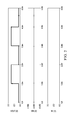
FIG. 2 is an diagram depicting an example of the operation of the IC of FIG. 1.
DETAILED DESCRIPTION
Refer now to the drawings wherein depicted elements are, for the sake of clarity, not necessarily shown to scale and wherein like or similar elements are designated by the same reference numeral through the several views.
Turning to FIG. 1, an IC 100 in accordance with a preferred embodiment of the present invention can be seen. Typically, the IC 100 includes an input pin VIN, an output pin VOUT, a ground pin GND, an enable pin VON, load switch Q7 (which can, for example, be an NMOS transistor), a level shifter 102, and a slew rate controller 104. The level shifter 102 generally comprises a current control circuit (i.e., resistor R1), a current mirror (i.e., NMOS transistors Q3 and Q2), transistor Q1 (which can, for example, be a PMOS transistor), and a voltage divider or impedance network (i.e., resistors R2 and R3). The slew rate controller 104 generally comprises inverter 106, transistors Q5 and Q6 (which can, for example, be a PMOS transistor and an NMOS transistor, respectively), and an impedance network (i.e., resistor R4).
In operation, the control circuit (which is generally formed by level shifter 104 and slew control circuit 104) uses the ground pin GND as a positive supply rail and the input pin VIN as an internal ground to generate a negative output voltage at output pin VOUT. This can be accomplished because a negative voltage is applied to the input pin VIN (i.e., −5V), which means the ground pin GND, which is coupled to that ground (i.e., 0V), has a higher voltage than the input pin VIN. When the enable signal or voltage (applied to the enable pin VON) is less than the threshold voltage of the transistor Q1, transistor Q1 is “off,” which pulls the input terminal of inverter 106 to the negative voltage (supplied through the input pin VIN) and which maintains the transistor Q7 (i.e., the load switch) in an “off” state. Once the enable signal becomes greater than the threshold voltage of transistor Q1, transistor Q1 turns “on.” With transistor Q1 in an “on” state, a steering current is generated through resistor R1 and transistor Q3 (which is diode-connected). This steering current is mirrored through resistors R2 and R3 and transistor Q1. Because the resistor R3 has a much larger resistance than resistor R2 (which generally limits the maximum gate-source voltage seen by transistor Q2 for both the “on” and “off” states of transistor Q1), the intermediate signal or voltage (at the node between resistors R2 and R3) becomes a fraction of the “on” voltage of transistor Q1, which enables inverter 106. The output of inverter 106 is applied to the gates of transistors Q5 and Q6, and (collectively with resistor R4) transistors Q5 and Q6 generate a slew-controlled intermediate signal or voltage at node N1, which (when the inverter 106 is enabled) is at ground. Because the voltage applied to the input terminal VIN is negative, the pulling of the gate of transistor Q7 to ground turns transistor Q7 “on,” enabling a negative output signal to be provided through output pin VOUT. Therefore, the output signal (at output pin VOUT) can be ground (applied to the ground pin GND) when transistor Q1 is “off” and can be the negative voltage (applied to the input pin VIN) when transistor Q1 is “on.”
Turning to FIG. 2, an example of the operation of IC 100 can be seen. In this example, the input voltage applied to input pin VIN is −5V. Additionally, as the enable signal (which is applied to the enable pin VON) toggles, the output signal from output pin VOUT toggles. Additionally, as shown, the slew-controlled intermediate signal (at node N1) toggles inversely with the output signal (at the output pint VOUT).
Having thus described the present invention by reference to certain of its preferred embodiments, it is noted that the embodiments disclosed are illustrative rather than limiting in nature and that a wide range of variations, modifications, changes, and substitutions are contemplated in the foregoing disclosure and, in some instances, some features of the present invention may be employed without a corresponding use of the other features. Accordingly, it is appropriate that the appended claims be construed broadly and in a manner consistent with the scope of the invention.

Claims (10)

The invention claimed is:
1. An integrated circuit (IC) comprising:
an enable pin;
a ground pin;
an input pin;
an output pin;
a load switch that is coupled between the input pin and the output pin, wherein the load switch receives a negative voltage through the input pin; and
control circuitry that is coupled to the enable pin, the ground pin, and the load switch, wherein the control circuitry controls the load switch, and wherein the control circuitry uses the ground pin as a positive supply rail and the input pin as an internal ground,
wherein the control circuitry further comprises:
a level shifter that is coupled to the ground pin, the input pin, and the enable pin; and
a slew rate controller that is coupled to the level shifter, the input pin, and the load switch,
wherein the level shifter further comprises:
a current mirror that is coupled to the input pin;
a current control circuit that is coupled between the ground pin and the current mirror;
a transistor having a first passive electrode, a second passive electrode, and a control electrode, wherein the control electrode of the transistor is coupled to the ground pin, and wherein the first passive electrode of the transistor is coupled to the enable pin; and
an impedance network that is coupled between the second passive electrode of the transistor and the current mirror and that is coupled to the slew rate controller.
2. The IC of claim 1, wherein the impedance network further comprises a first impedance network, and wherein the transistor further comprise a first transistor, and wherein the slew rate controller further comprises:
an inverter having a first power terminal, a second power terminal, an input terminal, and an output terminal, wherein the first power terminal of the inverter is coupled to the ground pin, and wherein the second power terminal of the inverter is coupled to the input pin, and wherein the input terminal of the inverter is coupled to the first impedance network;
a second transistor having a first passive electrode, a second passive electrode, and a control electrode, wherein the control electrode of the second transistor is coupled to the output terminal of the inverter, and wherein the first passive electrode of the second transistor is coupled to the ground pin;
a second impedance network that is coupled to the second passive electrode of the second transistor and the load switch; and
a third transistor having a first passive electrode, a second passive electrode, and a control electrode, wherein the control electrode of the third transistor is coupled to the output terminal of the inverter, and wherein the first passive electrode of the third transistor is coupled to the second impedance network, and wherein the second passive electrode of the third transistor is coupled to the input pin.
3. The apparatus of claim 2, wherein the first impedance network further comprises a plurality of resistors coupled in series with one another.
4. The apparatus of claim 2, wherein the first, second, and third transistors further comprise a first PMOS transistor, a second PMOS transistor, and an NMOS transistor.
5. A method comprising:
level shifting an enable signal to generate an intermediate signal by using input pin as an in as an internal ground and ground pin as a positive supply rail, wherein a negative voltage is applied to the input pin;
controlling the skew of the intermediate signal; and
activating a load switch with a skew-controlled intermediate signal, wherein the load switch is coupled between an output pin and the input,
wherein the step of level shifting further comprises:
generating a steering current between the ground pin and the input pin;
activating a first transistor when the enable signal becomes greater than the threshold voltage of the first transistor;
mirroring the steering current when the first transistor is activated;
dividing the enable signal to generate the intermediate signal; and
applying the intermediate signal to a skew rate controller so as to generate the skew-controlled intermediate signal.
6. The method of claim 5, wherein the load switch further comprises an NMOS transistor, and wherein the step of activating the load switch further comprises pulling the gate of the NMOS transistor to ground.
7. An IC comprising:
an enable pin;
a ground pin;
an input pin;
an output pin;
a NMOS transistor that is coupled to the output pin at its drain and the input pin at its source, wherein the a negative voltage is applied to the source of the NMOS transistor through the input pin; and
control circuitry that is coupled to the enable pin, the ground pin, and the load switch, wherein the control circuitry controls the load switch, and wherein the control circuitry uses the ground pin as a positive supply rail and the input pin as an internal ground,
wherein the control circuitry further comprises:
a level shifter that is coupled to the ground pin, the input pin, and the enable pin; and
a slew rate controller that is coupled to the level shifter, the input pin, and the load switch,
wherein the level shifter further comprises:
a current mirror that is coupled to the input pin;
a resistor that is coupled between the ground pin and the current mirror;
a PMOS transistor that is coupled to the ground pin at its gate and the enable pin at its source; and
an voltage divider that is coupled between the drain of the PMOS transistor and the current mirror.
8. The IC of claim 7, wherein the NMOS transistor further comprises a first NMOS transistor, and wherein the resistor further comprises a first resistor, and wherein the slew rate controller further comprises:
an inverter having a first power terminal, a second power terminal, an input terminal, and an output terminal, wherein the first power terminal of the inverter is coupled to the ground pin, and wherein the second power terminal of the inverter is coupled to the input pin, and wherein the input terminal of the inverter is coupled to the voltage divider;
a second PMOS transistor that is coupled to the output terminal of the inverter at its gate and the ground pin at its source;
a second resistor that is coupled to the drain of the second PMOS transistor and the gate of the first NMOS transistor; and
a second NMOS transistor that is coupled to the output terminal of the inverter at its gate, the second resistor at its drain, and the input pin at its source.
9. The apparatus of claim 8, wherein the voltage divider further comprises:
a third resistor that is coupled between the drain of the first PMOS transistor and the input terminal of the inverter; and
a fourth resistor that is coupled between the input terminal of the inverter and the current mirror.
10. The apparatus of claim 9, wherein the current mirror further comprises:
a third NMOS transistor that is coupled to the first resistor at its drain and gate and the input pin at its source; and
a fourth NMOS transistor that is coupled to the fourth resistor at its drain, the gate of the third NMOS transistor at its gate, and the input pin at its source.
US13/786,151 2013-03-05 2013-03-05 Load switch Active US8854097B2 (en)

Priority Applications (4)

Application Number Priority Date Filing Date Title
US13/786,151 US8854097B2 (en) 2013-03-05 2013-03-05 Load switch
EP14760468.0A EP2992607B1 (en) 2013-03-05 2014-03-05 Load switch
CN201480011810.5A CN105009453B (en) 2013-03-05 2014-03-05 Load switch
PCT/US2014/020765 WO2014138243A1 (en) 2013-03-05 2014-03-05 Load switch

Applications Claiming Priority (1)

Application Number Priority Date Filing Date Title
US13/786,151 US8854097B2 (en) 2013-03-05 2013-03-05 Load switch

Publications (2)

Publication Number Publication Date
US20140253194A1 US20140253194A1 (en) 2014-09-11
US8854097B2 true US8854097B2 (en) 2014-10-07

Family

ID=51487106

Family Applications (1)

Application Number Title Priority Date Filing Date
US13/786,151 Active US8854097B2 (en) 2013-03-05 2013-03-05 Load switch

Country Status (4)

Country Link
US (1) US8854097B2 (en)
EP (1) EP2992607B1 (en)
CN (1) CN105009453B (en)
WO (1) WO2014138243A1 (en)

Families Citing this family (4)

* Cited by examiner, † Cited by third party
Publication number Priority date Publication date Assignee Title
TWI575858B (en) * 2015-10-07 2017-03-21 晨星半導體股份有限公司 Switched-mode voltage converter
US10468983B2 (en) * 2015-11-05 2019-11-05 Silicon Laboratories Inc. Slew-rate controlled supply voltage switching
US11239831B2 (en) * 2020-06-24 2022-02-01 Texas Instruments Incorporated Level shifter
CN113556119B (en) * 2021-09-18 2021-12-07 成都万创科技股份有限公司 Mis-connection prevention switchable isolated digital input circuit

Citations (2)

* Cited by examiner, † Cited by third party
Publication number Priority date Publication date Assignee Title
US7061291B2 (en) * 2003-09-08 2006-06-13 Texas Instruments Incorporated Linear voltage tracking amplifier for negative supply slew rate control
US20090289692A1 (en) 2008-05-21 2009-11-26 Ting Huei Chen Nagative voltage switch

Family Cites Families (3)

* Cited by examiner, † Cited by third party
Publication number Priority date Publication date Assignee Title
CN100541569C (en) * 2004-08-30 2009-09-16 松下电器产业株式会社 Driving circuit
US7705630B1 (en) * 2009-05-20 2010-04-27 Ememory Technology Inc. Negative voltage level shifter having simplified structure
CN102904565B (en) * 2012-10-09 2014-05-28 长安大学 Level shift circuit for DC-DC (Direct Current) driven ultra-low static current

Patent Citations (2)

* Cited by examiner, † Cited by third party
Publication number Priority date Publication date Assignee Title
US7061291B2 (en) * 2003-09-08 2006-06-13 Texas Instruments Incorporated Linear voltage tracking amplifier for negative supply slew rate control
US20090289692A1 (en) 2008-05-21 2009-11-26 Ting Huei Chen Nagative voltage switch

Also Published As

Publication number Publication date
US20140253194A1 (en) 2014-09-11
EP2992607B1 (en) 2018-08-29
CN105009453A (en) 2015-10-28
CN105009453B (en) 2018-08-28
EP2992607A1 (en) 2016-03-09
WO2014138243A1 (en) 2014-09-12
EP2992607A4 (en) 2017-03-22

Similar Documents

Publication Publication Date Title
US8847659B1 (en) Systems and method for level shifters
CN107342685B (en) DCDC converter
JP6082356B2 (en) Semiconductor device
US9459639B2 (en) Power supply circuit with control unit
US8854097B2 (en) Load switch
KR20170131452A (en) Drive for cascode stack of power FETs
CN104142702A (en) Output circuit and voltage signal output method
JP2018513613A5 (en)
US20160187900A1 (en) Voltage regulator circuit and method for limiting inrush current
US9660651B2 (en) Level shift circuit
JP2019007823A (en) Semiconductor integrated device and gate screening test method thereof
CN103955251B (en) High-voltage linear voltage regulator
JP5806972B2 (en) Output driver circuit
EP3308240B1 (en) Start-up circuit
US7902904B2 (en) Bias circuit scheme for improved reliability in high voltage supply with low voltage device
US20160182040A1 (en) Audio switch circuit with slow turn-on
US20150137856A1 (en) Input circuit with mirroring
US10033358B2 (en) Buffer circuit and voltage generator using the same
US20140152288A1 (en) Reference Voltage Generator and Corresponding Integrated Circuit
US20140253057A1 (en) Compensation Scheme to Improve the Stability of the Operational Amplifiers
TW201823908A (en) Voltage dividers
US10320351B1 (en) Switch for controlling a gain of an amplifier and method thereof
US10691151B2 (en) Devices and methods for dynamic overvoltage protection in regulators
JP2014085745A (en) Reference voltage generation circuit
JP5689778B2 (en) Input circuit

Legal Events

Date Code Title Description
AS Assignment

Owner name: TEXAS INSTRUMENTS INCORPORATED, TEXAS

Free format text: ASSIGNMENT OF ASSIGNORS INTEREST;ASSIGNORS:SADATE, ALINE C.;GROSE, WILLIAM E.;REEL/FRAME:029938/0491

Effective date: 20130305

STCF Information on status: patent grant

Free format text: PATENTED CASE

MAFP Maintenance fee payment

Free format text: PAYMENT OF MAINTENANCE FEE, 4TH YEAR, LARGE ENTITY (ORIGINAL EVENT CODE: M1551)

Year of fee payment: 4

MAFP Maintenance fee payment

Free format text: PAYMENT OF MAINTENANCE FEE, 8TH YEAR, LARGE ENTITY (ORIGINAL EVENT CODE: M1552); ENTITY STATUS OF PATENT OWNER: LARGE ENTITY

Year of fee payment: 8