US8846489B2 - Method for forming trench isolation - Google Patents
Method for forming trench isolation Download PDFInfo
- Publication number
- US8846489B2 US8846489B2 US13/628,051 US201213628051A US8846489B2 US 8846489 B2 US8846489 B2 US 8846489B2 US 201213628051 A US201213628051 A US 201213628051A US 8846489 B2 US8846489 B2 US 8846489B2
- Authority
- US
- United States
- Prior art keywords
- trench
- layer
- spacer
- substrate
- hard mask
- Prior art date
- Legal status (The legal status is an assumption and is not a legal conclusion. Google has not performed a legal analysis and makes no representation as to the accuracy of the status listed.)
- Expired - Fee Related
Links
Images


Classifications
-
- H—ELECTRICITY
- H10—SEMICONDUCTOR DEVICES; ELECTRIC SOLID-STATE DEVICES NOT OTHERWISE PROVIDED FOR
- H10W—GENERIC PACKAGES, INTERCONNECTIONS, CONNECTORS OR OTHER CONSTRUCTIONAL DETAILS OF DEVICES COVERED BY CLASS H10
- H10W10/00—Isolation regions in semiconductor bodies between components of integrated devices
- H10W10/01—Manufacture or treatment
- H10W10/011—Manufacture or treatment of isolation regions comprising dielectric materials
- H10W10/014—Manufacture or treatment of isolation regions comprising dielectric materials using trench refilling with dielectric materials, e.g. shallow trench isolations
-
- H—ELECTRICITY
- H10—SEMICONDUCTOR DEVICES; ELECTRIC SOLID-STATE DEVICES NOT OTHERWISE PROVIDED FOR
- H10W—GENERIC PACKAGES, INTERCONNECTIONS, CONNECTORS OR OTHER CONSTRUCTIONAL DETAILS OF DEVICES COVERED BY CLASS H10
- H10W10/00—Isolation regions in semiconductor bodies between components of integrated devices
- H10W10/10—Isolation regions comprising dielectric materials
- H10W10/13—Isolation regions comprising dielectric materials formed using local oxidation of silicon [LOCOS], e.g. sealed interface localised oxidation [SILO] or side-wall mask isolation [SWAMI]
-
- H—ELECTRICITY
- H10—SEMICONDUCTOR DEVICES; ELECTRIC SOLID-STATE DEVICES NOT OTHERWISE PROVIDED FOR
- H10W—GENERIC PACKAGES, INTERCONNECTIONS, CONNECTORS OR OTHER CONSTRUCTIONAL DETAILS OF DEVICES COVERED BY CLASS H10
- H10W10/00—Isolation regions in semiconductor bodies between components of integrated devices
- H10W10/01—Manufacture or treatment
- H10W10/011—Manufacture or treatment of isolation regions comprising dielectric materials
- H10W10/012—Manufacture or treatment of isolation regions comprising dielectric materials using local oxidation of silicon [LOCOS]
- H10W10/0121—Manufacture or treatment of isolation regions comprising dielectric materials using local oxidation of silicon [LOCOS] in regions recessed from the surface, e.g. in trenches or grooves
-
- H—ELECTRICITY
- H10—SEMICONDUCTOR DEVICES; ELECTRIC SOLID-STATE DEVICES NOT OTHERWISE PROVIDED FOR
- H10W—GENERIC PACKAGES, INTERCONNECTIONS, CONNECTORS OR OTHER CONSTRUCTIONAL DETAILS OF DEVICES COVERED BY CLASS H10
- H10W10/00—Isolation regions in semiconductor bodies between components of integrated devices
- H10W10/10—Isolation regions comprising dielectric materials
- H10W10/17—Isolation regions comprising dielectric materials formed using trench refilling with dielectric materials, e.g. shallow trench isolations
-
- H—ELECTRICITY
- H10—SEMICONDUCTOR DEVICES; ELECTRIC SOLID-STATE DEVICES NOT OTHERWISE PROVIDED FOR
- H10P—GENERIC PROCESSES OR APPARATUS FOR THE MANUFACTURE OR TREATMENT OF DEVICES COVERED BY CLASS H10
- H10P14/00—Formation of materials, e.g. in the shape of layers or pillars
- H10P14/60—Formation of materials, e.g. in the shape of layers or pillars of insulating materials
- H10P14/61—Formation of materials, e.g. in the shape of layers or pillars of insulating materials using masks
-
- H—ELECTRICITY
- H10—SEMICONDUCTOR DEVICES; ELECTRIC SOLID-STATE DEVICES NOT OTHERWISE PROVIDED FOR
- H10P—GENERIC PROCESSES OR APPARATUS FOR THE MANUFACTURE OR TREATMENT OF DEVICES COVERED BY CLASS H10
- H10P14/00—Formation of materials, e.g. in the shape of layers or pillars
- H10P14/60—Formation of materials, e.g. in the shape of layers or pillars of insulating materials
- H10P14/63—Formation of materials, e.g. in the shape of layers or pillars of insulating materials characterised by the formation processes
- H10P14/6302—Non-deposition formation processes
- H10P14/6304—Formation by oxidation, e.g. oxidation of the substrate
- H10P14/6306—Formation by oxidation, e.g. oxidation of the substrate of the semiconductor materials
- H10P14/6308—Formation by oxidation, e.g. oxidation of the substrate of the semiconductor materials of Group IV semiconductors
- H10P14/6309—Formation by oxidation, e.g. oxidation of the substrate of the semiconductor materials of Group IV semiconductors of silicon in uncombined form, i.e. pure silicon
-
- H—ELECTRICITY
- H10—SEMICONDUCTOR DEVICES; ELECTRIC SOLID-STATE DEVICES NOT OTHERWISE PROVIDED FOR
- H10P—GENERIC PROCESSES OR APPARATUS FOR THE MANUFACTURE OR TREATMENT OF DEVICES COVERED BY CLASS H10
- H10P50/00—Etching of wafers, substrates or parts of devices
- H10P50/69—Etching of wafers, substrates or parts of devices using masks for semiconductor materials
- H10P50/691—Etching of wafers, substrates or parts of devices using masks for semiconductor materials for Group V materials or Group III-V materials
- H10P50/693—Etching of wafers, substrates or parts of devices using masks for semiconductor materials for Group V materials or Group III-V materials characterised by their size, orientation, disposition, behaviour or shape, in horizontal or vertical plane
- H10P50/695—Etching of wafers, substrates or parts of devices using masks for semiconductor materials for Group V materials or Group III-V materials characterised by their size, orientation, disposition, behaviour or shape, in horizontal or vertical plane characterised by the process involved to create the mask, e.g. lift-off masks or sidewalls or to modify the mask
Definitions
- the present invention relates generally to the field of semiconductor process. More particularly, the present invention relates to a trench isolation process that utilizes spacer process and/or thermal oxidation to achieve void-free trench fill.
- LOCOS Local oxidation of silicon
- STI shallow trench isolation
- the STI process includes first etching trench around the active area and then filling the trench with insulating material to isolate the active area.
- a trench isolation method is disclosed.
- a substrate having thereon a pad layer and a hard mask is provided.
- An opening is formed in the hard mask.
- the substrate is etched through the opening to thereby form a first trench.
- a spacer is formed on a sidewall of the first trench.
- a second trench is then etched into the substrate through the first trench by using the spacer as an etching hard mask.
- the substrate within the second trench is then oxidized by using the spacer as an oxidation protection layer, thereby forming an oxide layer that fills the second trench.
- the spacer is then removed to reveal the sidewall of the first trench.
- a liner layer is then formed on the revealed sidewall of the first trench.
- a chemical vapor deposition process is then performed to deposit a dielectric layer that fills the first trench.
- a trench isolation method is disclosed.
- a substrate having thereon a pad layer and a hard mask layer is provided. At least one opening is then formed in the hard mask layer.
- a spacer is then formed on a sidewall of the opening.
- the substrate is etched through the opening to thereby form a trench.
- a thermal oxidation process is performed, using the spacer as a protection layer, to oxidize the substrate within the trench until the trench is completely filled up with an oxide layer.
- a trench isolation method is disclosed.
- a substrate having thereon a pad layer and a hard mask layer is provided. At least one opening is then formed in the hard mask layer.
- the substrate is then etched through the opening to a predetermined depth, thereby forming a recess region.
- a spacer is formed on a sidewall of the opening.
- the substrate is then etched through the opening and the recess region to thereby form a trench.
- a thermal oxidation process is performed, using the spacer as a protection layer, to oxidize the substrate within the trench until the trench is completely filled up with an oxide layer.
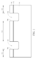
- FIGS. 1-4 are schematic, cross-sectional diagrams showing a method for forming trench isolation in accordance with one embodiment of the invention.
- FIGS. 5-7 are schematic, cross-sectional diagrams showing a method for forming trench isolation in accordance with another embodiment of the invention.
- FIGS. 8-10 are schematic, cross-sectional diagrams showing a method for forming trench isolation in accordance with still another embodiment of the invention.
- FIGS. 1-4 are schematic, cross-sectional diagrams showing a method for forming trench isolation in accordance with one embodiment of the invention.
- a substrate 10 such as a semiconductor substrate is provided.
- a pad layer 12 and a hard mask layer 14 are formed on a top surface of the substrate 10 .
- the pad layer 12 may be an oxide pad layer
- the hard mask layer 14 may be a silicon nitride hard mask layer.
- the hard mask layer 14 may be a multi-layer structure, for example, a silicon nitride layer and a silicon oxide layer.
- a lithographic process and an etching process are performed to form openings 14 a in the hard mask layer 14 .
- the patterned hard mask layer 14 substantially defines active areas. Using the hard mask layer 14 as an etching hard mask, the pad layer 12 and the substrate 10 are etched to a first predetermined depth through the openings 14 a , thereby forming first trenches 102 .
- a spacer 16 such as silicon nitride spacer is then formed on a sidewall of the first trench 102 .
- the method of forming the spacer 16 may include depositing a conformal silicon nitride layer covering the hard mask layer 16 and the sidewall and bottom of the first trench 102 , and then anisotropically etching the silicon nitride layer.
- a dry etching process is performed, using the spacer 16 as an etching hard mask, to continue to etch the substrate 10 to a second predetermined depth through the first trench 102 , thereby forming a second trench 104 directly under each of the first trenches 102 .
- the trench width of the second trench 104 may be controlled by the width or thickness of the spacer 16 .
- a thermal oxidation process is carried out, for example, at a temperature between 800-1200° C., using steam, oxygen, or steam or oxygen containing hydrogen chloride or nitrogen, under process pressure ranging 600-760 torr.
- the spacer 16 acts as a protection layer.
- the substrate 10 within the second trench 104 is oxidized until the second trench 104 is completely filled with an oxide layer 18 .
- a wedge-shaped recess structure 18 a is formed on the top surface of the oxide layer 18 .
- the spacer 16 is then removed thereby exposing the sidewall of the first trench 102 .
- An oxidation process is then performed to form an oxide liner layer 20 on the exposed sidewall of the first trench 102 .
- a chemical vapor deposition (CVD) process is performed to deposit a dielectric layer 22 such as a silicon oxide layer in a blanket manner.
- the dielectric layer 22 fills the first trench 102 . Since the second trench 104 is filled with thermally formed oxide layer 18 which reduces the aspect ratio, the subsequent CVD process for trench filling the first trench 102 may have larger process window, and a high-quality, seamless or void-free trench isolation can be achieved.
- FIGS. 5-7 are schematic, cross-sectional diagrams showing a method for forming trench isolation in accordance with another embodiment of the invention.
- a substrate 10 such as a semiconductor substrate is provided.
- a pad layer 12 and a hard mask layer 14 are formed on a top surface of the substrate 10 .
- the pad layer 12 may be an oxide pad layer
- the hard mask layer 14 may be a silicon nitride hard mask layer.
- the hard mask layer 14 may be a multi-layer structure, for example, a silicon nitride layer and a silicon oxide layer.
- a lithographic process and an etching process are performed to form openings 14 a in the hard mask layer 14 .
- a spacer 16 such as silicon nitride spacer is then formed on a sidewall of the opening 14 a .
- the method of forming the spacer 16 may include depositing a conformal silicon nitride layer covering the hard mask layer 16 and the sidewall and bottom of the opening 14 a , and then anisotropically etching the silicon nitride layer.
- a dry etching process is performed, using the spacer 16 as an etching hard mask, to continue to etch the substrate 10 to a predetermined depth through the opening 14 a , thereby forming a trench 114 directly under each of the openings 14 a .
- the trench width of the trench 114 may be controlled by the width or thickness of the spacer 16 .
- the spacer 16 may have a thickness that is smaller than a quarter of a width of the opening 14 a.
- a thermal oxidation process is carried out, for example, at a temperature between 800-1200° C., using steam, oxygen, or steam or oxygen containing hydrogen chloride or nitrogen, under process pressure ranging 600-760 torr.
- the spacer 16 acts as a protection layer.
- the substrate 10 within the second trench 104 is oxidized until the trench 114 is completely filled with an oxide layer 18 .
- a wedge-shaped recess structure 18 a is formed on the top surface of the oxide layer 18 .
- a slight bird's beak 18 b is formed.
- the width of the isolation trench can be reduced and integration of device can be increased.
- FIGS. 8-10 are schematic, cross-sectional diagrams showing a method for forming trench isolation in accordance with still another embodiment of the invention.
- a substrate 10 such as a semiconductor substrate is provided.
- a pad layer 12 and a hard mask layer 14 are formed on a top surface of the substrate 10 .
- the pad layer 12 may be an oxide pad layer
- the hard mask layer 14 may be a silicon nitride hard mask layer.
- the hard mask layer 14 may be a multi-layer structure, for example, a silicon nitride layer and a silicon oxide layer.
- a lithographic process and an etching process are performed to form openings 14 a in the hard mask layer 14 .
- the substrate 10 is etched to a first predetermined depth (smaller than 0.2 micrometers) through the openings 14 a , thereby forming a recess region 122 .
- a spacer 16 such as silicon nitride spacer is then formed on a sidewall of the opening 14 a .
- the method of forming the spacer 16 may include depositing a conformal silicon nitride layer covering the hard mask layer 16 and the sidewall and bottom of the opening 14 a , and then anisotropically etching the silicon nitride layer.
- a dry etching process is performed, using the spacer 16 as an etching hard mask, to continue to etch the substrate 10 to a second predetermined depth through the opening 14 a and the recess region 122 , thereby forming a trench 124 .
- the trench width of the trench 124 may be controlled by the width or thickness of the spacer 16 .
- a thermal oxidation process is carried out, for example, at a temperature between 800-1200° C., using steam, oxygen, or steam or oxygen containing hydrogen chloride or nitrogen, under process pressure ranging 600-760 torr.
- the spacer 16 acts as a protection layer.
- the substrate 10 within the trench 124 is oxidized until the trench 124 is completely filled with an oxide layer 18 .
- a wedge-shaped recess structure 18 a is formed on the top surface of the oxide layer 18 .
- a slight bird's beak 18 b is formed.
- the spacer 16 can protect the corners around the active area, therefore the bird's beak 18 b in FIG. 10 extends less into the active area.
Landscapes
- Element Separation (AREA)
Abstract
Description
Claims (7)
Priority Applications (1)
| Application Number | Priority Date | Filing Date | Title |
|---|---|---|---|
| US14/100,023 US20140087540A1 (en) | 2012-08-28 | 2013-12-09 | Method for forming trench isolation |
Applications Claiming Priority (3)
| Application Number | Priority Date | Filing Date | Title |
|---|---|---|---|
| TW101131197 | 2012-08-28 | ||
| TW101131197A | 2012-08-28 | ||
| TW101131197A TWI470733B (en) | 2012-08-28 | 2012-08-28 | Ditch insulation process |
Related Child Applications (1)
| Application Number | Title | Priority Date | Filing Date |
|---|---|---|---|
| US14/100,023 Continuation US20140087540A1 (en) | 2012-08-28 | 2013-12-09 | Method for forming trench isolation |
Publications (2)
| Publication Number | Publication Date |
|---|---|
| US20140065795A1 US20140065795A1 (en) | 2014-03-06 |
| US8846489B2 true US8846489B2 (en) | 2014-09-30 |
Family
ID=50188129
Family Applications (2)
| Application Number | Title | Priority Date | Filing Date |
|---|---|---|---|
| US13/628,051 Expired - Fee Related US8846489B2 (en) | 2012-08-28 | 2012-09-27 | Method for forming trench isolation |
| US14/100,023 Abandoned US20140087540A1 (en) | 2012-08-28 | 2013-12-09 | Method for forming trench isolation |
Family Applications After (1)
| Application Number | Title | Priority Date | Filing Date |
|---|---|---|---|
| US14/100,023 Abandoned US20140087540A1 (en) | 2012-08-28 | 2013-12-09 | Method for forming trench isolation |
Country Status (3)
| Country | Link |
|---|---|
| US (2) | US8846489B2 (en) |
| CN (1) | CN103681452B (en) |
| TW (1) | TWI470733B (en) |
Cited By (2)
| Publication number | Priority date | Publication date | Assignee | Title |
|---|---|---|---|---|
| US20150279957A1 (en) * | 2014-03-31 | 2015-10-01 | United Microelectronics Corp. | Semiconductor structure and manufacturing method for the same |
| US9449921B1 (en) * | 2015-12-15 | 2016-09-20 | International Business Machines Corporation | Voidless contact metal structures |
Families Citing this family (9)
| Publication number | Priority date | Publication date | Assignee | Title |
|---|---|---|---|---|
| US9385030B2 (en) | 2014-04-30 | 2016-07-05 | Globalfoundries Inc. | Spacer to prevent source-drain contact encroachment |
| CN105448807B (en) * | 2015-11-20 | 2017-11-10 | 浙江正邦电子股份有限公司 | A kind of semiconductor device chip is to logical isolation manufacturing process |
| US20210351066A1 (en) * | 2017-12-29 | 2021-11-11 | United Microelectronics Corp. | Semiconductor device and method for fabricating the same |
| CN110911342A (en) * | 2018-09-14 | 2020-03-24 | 长鑫存储技术有限公司 | Shallow trench isolation structure and method of making the same |
| KR102806796B1 (en) * | 2019-04-08 | 2025-05-16 | 삼성전자주식회사 | Semiconductor device |
| CN111799329B (en) * | 2019-04-08 | 2024-11-29 | 三星电子株式会社 | Semiconductor device with a semiconductor layer having a plurality of semiconductor layers |
| TWI750881B (en) | 2020-11-04 | 2021-12-21 | 華邦電子股份有限公司 | Isolation structure and manufacturing method thereof |
| CN114582792B (en) * | 2020-11-30 | 2025-07-29 | 华邦电子股份有限公司 | Isolation structure and manufacturing method thereof |
| CN113782484A (en) * | 2021-11-11 | 2021-12-10 | 广州粤芯半导体技术有限公司 | Manufacturing method of semiconductor device |
Citations (8)
| Publication number | Priority date | Publication date | Assignee | Title |
|---|---|---|---|---|
| US6018174A (en) * | 1998-04-06 | 2000-01-25 | Siemens Aktiengesellschaft | Bottle-shaped trench capacitor with epi buried layer |
| US6251750B1 (en) * | 1999-09-15 | 2001-06-26 | United Microelectronics Corp. | Method for manufacturing shallow trench isolation |
| US20060089008A1 (en) * | 2004-10-27 | 2006-04-27 | Eunkee Hong | Methods of manufacturing silicon oxide isolation layers and semiconductor devices that include such isolation layers |
| US20070235835A1 (en) | 2005-03-10 | 2007-10-11 | Taiwan Semiconductor Manufacturing Company, Ltd. | Shallow trench isolation structure for semiconductor device |
| US20080048186A1 (en) * | 2006-03-30 | 2008-02-28 | International Business Machines Corporation | Design Structures Incorporating Semiconductor Device Structures with Self-Aligned Doped Regions |
| US20080220586A1 (en) * | 2005-10-28 | 2008-09-11 | International Business Machines Corporation | Methods for forming semiconductor structures with buried isolation collars and semiconductor structures formed by these methods |
| US7470588B2 (en) * | 2005-09-22 | 2008-12-30 | Samsung Electronics Co., Ltd. | Transistors including laterally extended active regions and methods of fabricating the same |
| TW200926353A (en) | 2007-07-13 | 2009-06-16 | Marvell World Trade Ltd | Method for shallow trench isolation |
Family Cites Families (1)
| Publication number | Priority date | Publication date | Assignee | Title |
|---|---|---|---|---|
| US6146970A (en) * | 1998-05-26 | 2000-11-14 | Motorola Inc. | Capped shallow trench isolation and method of formation |
-
2012
- 2012-08-28 TW TW101131197A patent/TWI470733B/en not_active IP Right Cessation
- 2012-09-27 US US13/628,051 patent/US8846489B2/en not_active Expired - Fee Related
- 2012-10-09 CN CN201210378608.9A patent/CN103681452B/en not_active Expired - Fee Related
-
2013
- 2013-12-09 US US14/100,023 patent/US20140087540A1/en not_active Abandoned
Patent Citations (8)
| Publication number | Priority date | Publication date | Assignee | Title |
|---|---|---|---|---|
| US6018174A (en) * | 1998-04-06 | 2000-01-25 | Siemens Aktiengesellschaft | Bottle-shaped trench capacitor with epi buried layer |
| US6251750B1 (en) * | 1999-09-15 | 2001-06-26 | United Microelectronics Corp. | Method for manufacturing shallow trench isolation |
| US20060089008A1 (en) * | 2004-10-27 | 2006-04-27 | Eunkee Hong | Methods of manufacturing silicon oxide isolation layers and semiconductor devices that include such isolation layers |
| US20070235835A1 (en) | 2005-03-10 | 2007-10-11 | Taiwan Semiconductor Manufacturing Company, Ltd. | Shallow trench isolation structure for semiconductor device |
| US7470588B2 (en) * | 2005-09-22 | 2008-12-30 | Samsung Electronics Co., Ltd. | Transistors including laterally extended active regions and methods of fabricating the same |
| US20080220586A1 (en) * | 2005-10-28 | 2008-09-11 | International Business Machines Corporation | Methods for forming semiconductor structures with buried isolation collars and semiconductor structures formed by these methods |
| US20080048186A1 (en) * | 2006-03-30 | 2008-02-28 | International Business Machines Corporation | Design Structures Incorporating Semiconductor Device Structures with Self-Aligned Doped Regions |
| TW200926353A (en) | 2007-07-13 | 2009-06-16 | Marvell World Trade Ltd | Method for shallow trench isolation |
Cited By (6)
| Publication number | Priority date | Publication date | Assignee | Title |
|---|---|---|---|---|
| US20150279957A1 (en) * | 2014-03-31 | 2015-10-01 | United Microelectronics Corp. | Semiconductor structure and manufacturing method for the same |
| US9711646B2 (en) * | 2014-03-31 | 2017-07-18 | United Microelectronics Corp. | Semiconductor structure and manufacturing method for the same |
| US9876116B2 (en) | 2014-03-31 | 2018-01-23 | United Microelectronics Corp. | Semiconductor structure and manufacturing method for the same |
| US9449921B1 (en) * | 2015-12-15 | 2016-09-20 | International Business Machines Corporation | Voidless contact metal structures |
| US9859216B2 (en) | 2015-12-15 | 2018-01-02 | International Business Machines Corporation | Voidless contact metal structures |
| US9997407B2 (en) | 2015-12-15 | 2018-06-12 | International Business Machines Corporation | Voidless contact metal structures |
Also Published As
| Publication number | Publication date |
|---|---|
| TW201409611A (en) | 2014-03-01 |
| US20140087540A1 (en) | 2014-03-27 |
| CN103681452B (en) | 2016-04-20 |
| US20140065795A1 (en) | 2014-03-06 |
| CN103681452A (en) | 2014-03-26 |
| TWI470733B (en) | 2015-01-21 |
Similar Documents
| Publication | Publication Date | Title |
|---|---|---|
| US8846489B2 (en) | Method for forming trench isolation | |
| US20090184402A1 (en) | Method of fabricating a shallow trench isolation structure including forming a second liner covering the corner of the trench and first liner. | |
| JP2009021569A (en) | Semiconductor device having STI structure and manufacturing method thereof | |
| US10643883B2 (en) | Method of forming isolation structure | |
| JP2010027904A (en) | Method of manufacturing semiconductor device | |
| KR20100059297A (en) | Method for fabricating semiconductor device | |
| TW201017816A (en) | Semiconductor device and method for manufacturing the same | |
| KR20140137222A (en) | Semiconductor apparatus and manufacturing method of the same | |
| US20030162364A1 (en) | Method of forming shallow trench isolation in a substrate | |
| KR100875346B1 (en) | Method for manufacturing cell trench isolation film | |
| KR100559042B1 (en) | Shallow Trench Isolation Method for Semiconductor Devices | |
| KR100701699B1 (en) | Device Separating Method of Semiconductor Device | |
| KR101078720B1 (en) | Method for forming isolation layer of semiconductor device | |
| KR100550635B1 (en) | Semiconductor device and manufacturing method thereof | |
| KR100707593B1 (en) | Double device isolation structure of semiconductor device and its formation method | |
| KR20090128914A (en) | Trench gap fill method of semiconductor device | |
| KR100758494B1 (en) | Isolation Regions of Semiconductor Devices and Formation Methods | |
| KR100924544B1 (en) | Device Separating Method of Semiconductor Device | |
| KR20100078251A (en) | Method for manufacturing the semiconductor device | |
| KR20070090626A (en) | Device Separating Method of Semiconductor Device | |
| KR20070001421A (en) | Trench type isolation layer formation method of semiconductor device | |
| KR20090063656A (en) | Device Separator Formation Method | |
| KR20060000350A (en) | Device isolation film and method for forming the semiconductor device | |
| US20080102597A1 (en) | Method for Preparing a Gate Oxide Layer | |
| US20070155125A1 (en) | Method for forming shallow trench isolation of semiconductor device |
Legal Events
| Date | Code | Title | Description |
|---|---|---|---|
| AS | Assignment |
Owner name: ANPEC ELECTRONICS CORPORATION, TAIWAN Free format text: ASSIGNMENT OF ASSIGNORS INTEREST;ASSIGNORS:LIN, YUNG-FA;CHANG, CHIA-HAO;REEL/FRAME:029033/0845 Effective date: 20120912 |
|
| FEPP | Fee payment procedure |
Free format text: MAINTENANCE FEE REMINDER MAILED (ORIGINAL EVENT CODE: REM.) |
|
| LAPS | Lapse for failure to pay maintenance fees |
Free format text: PATENT EXPIRED FOR FAILURE TO PAY MAINTENANCE FEES (ORIGINAL EVENT CODE: EXP.); ENTITY STATUS OF PATENT OWNER: SMALL ENTITY |
|
| STCH | Information on status: patent discontinuation |
Free format text: PATENT EXPIRED DUE TO NONPAYMENT OF MAINTENANCE FEES UNDER 37 CFR 1.362 |
|
| FP | Lapsed due to failure to pay maintenance fee |
Effective date: 20180930 |