US8841833B2 - Organic el display and method of manufacturing the same - Google Patents
Organic el display and method of manufacturing the same Download PDFInfo
- Publication number
- US8841833B2 US8841833B2 US13/016,536 US201113016536A US8841833B2 US 8841833 B2 US8841833 B2 US 8841833B2 US 201113016536 A US201113016536 A US 201113016536A US 8841833 B2 US8841833 B2 US 8841833B2
- Authority
- US
- United States
- Prior art keywords
- group
- organic
- emitting layer
- light
- molecular material
- Prior art date
- Legal status (The legal status is an assumption and is not a legal conclusion. Google has not performed a legal analysis and makes no representation as to the accuracy of the status listed.)
- Active, expires
Links
Images


Classifications
-
- H—ELECTRICITY
- H10—SEMICONDUCTOR DEVICES; ELECTRIC SOLID-STATE DEVICES NOT OTHERWISE PROVIDED FOR
- H10K—ORGANIC ELECTRIC SOLID-STATE DEVICES
- H10K50/00—Organic light-emitting devices
- H10K50/10—OLEDs or polymer light-emitting diodes [PLED]
- H10K50/11—OLEDs or polymer light-emitting diodes [PLED] characterised by the electroluminescent [EL] layers
- H10K50/125—OLEDs or polymer light-emitting diodes [PLED] characterised by the electroluminescent [EL] layers specially adapted for multicolour light emission, e.g. for emitting white light
-
- H01L51/5036—
-
- H01L27/3211—
-
- H01L51/0058—
-
- H01L51/0059—
-
- H01L51/006—
-
- H01L51/5004—
-
- H—ELECTRICITY
- H10—SEMICONDUCTOR DEVICES; ELECTRIC SOLID-STATE DEVICES NOT OTHERWISE PROVIDED FOR
- H10K—ORGANIC ELECTRIC SOLID-STATE DEVICES
- H10K50/00—Organic light-emitting devices
- H10K50/10—OLEDs or polymer light-emitting diodes [PLED]
- H10K50/11—OLEDs or polymer light-emitting diodes [PLED] characterised by the electroluminescent [EL] layers
-
- H—ELECTRICITY
- H10—SEMICONDUCTOR DEVICES; ELECTRIC SOLID-STATE DEVICES NOT OTHERWISE PROVIDED FOR
- H10K—ORGANIC ELECTRIC SOLID-STATE DEVICES
- H10K59/00—Integrated devices, or assemblies of multiple devices, comprising at least one organic light-emitting element covered by group H10K50/00
- H10K59/30—Devices specially adapted for multicolour light emission
- H10K59/35—Devices specially adapted for multicolour light emission comprising red-green-blue [RGB] subpixels
-
- H—ELECTRICITY
- H10—SEMICONDUCTOR DEVICES; ELECTRIC SOLID-STATE DEVICES NOT OTHERWISE PROVIDED FOR
- H10K—ORGANIC ELECTRIC SOLID-STATE DEVICES
- H10K85/00—Organic materials used in the body or electrodes of devices covered by this subclass
- H10K85/60—Organic compounds having low molecular weight
- H10K85/615—Polycyclic condensed aromatic hydrocarbons, e.g. anthracene
- H10K85/626—Polycyclic condensed aromatic hydrocarbons, e.g. anthracene containing more than one polycyclic condensed aromatic rings, e.g. bis-anthracene
-
- H—ELECTRICITY
- H10—SEMICONDUCTOR DEVICES; ELECTRIC SOLID-STATE DEVICES NOT OTHERWISE PROVIDED FOR
- H10K—ORGANIC ELECTRIC SOLID-STATE DEVICES
- H10K85/00—Organic materials used in the body or electrodes of devices covered by this subclass
- H10K85/60—Organic compounds having low molecular weight
- H10K85/631—Amine compounds having at least two aryl rest on at least one amine-nitrogen atom, e.g. triphenylamine
- H10K85/633—Amine compounds having at least two aryl rest on at least one amine-nitrogen atom, e.g. triphenylamine comprising polycyclic condensed aromatic hydrocarbons as substituents on the nitrogen atom
-
- H01L51/0039—
-
- H01L51/0043—
-
- H01L51/0081—
-
- H—ELECTRICITY
- H10—SEMICONDUCTOR DEVICES; ELECTRIC SOLID-STATE DEVICES NOT OTHERWISE PROVIDED FOR
- H10K—ORGANIC ELECTRIC SOLID-STATE DEVICES
- H10K2101/00—Properties of the organic materials covered by group H10K85/00
- H10K2101/40—Interrelation of parameters between multiple constituent active layers or sublayers, e.g. HOMO values in adjacent layers
-
- H—ELECTRICITY
- H10—SEMICONDUCTOR DEVICES; ELECTRIC SOLID-STATE DEVICES NOT OTHERWISE PROVIDED FOR
- H10K—ORGANIC ELECTRIC SOLID-STATE DEVICES
- H10K85/00—Organic materials used in the body or electrodes of devices covered by this subclass
- H10K85/10—Organic polymers or oligomers
- H10K85/111—Organic polymers or oligomers comprising aromatic, heteroaromatic, or aryl chains, e.g. polyaniline, polyphenylene or polyphenylene vinylene
- H10K85/115—Polyfluorene; Derivatives thereof
-
- H—ELECTRICITY
- H10—SEMICONDUCTOR DEVICES; ELECTRIC SOLID-STATE DEVICES NOT OTHERWISE PROVIDED FOR
- H10K—ORGANIC ELECTRIC SOLID-STATE DEVICES
- H10K85/00—Organic materials used in the body or electrodes of devices covered by this subclass
- H10K85/10—Organic polymers or oligomers
- H10K85/151—Copolymers
-
- H—ELECTRICITY
- H10—SEMICONDUCTOR DEVICES; ELECTRIC SOLID-STATE DEVICES NOT OTHERWISE PROVIDED FOR
- H10K—ORGANIC ELECTRIC SOLID-STATE DEVICES
- H10K85/00—Organic materials used in the body or electrodes of devices covered by this subclass
- H10K85/30—Coordination compounds
- H10K85/321—Metal complexes comprising a group IIIA element, e.g. Tris (8-hydroxyquinoline) gallium [Gaq3]
- H10K85/324—Metal complexes comprising a group IIIA element, e.g. Tris (8-hydroxyquinoline) gallium [Gaq3] comprising aluminium, e.g. Alq3
Definitions
- the present invention relates to an organic electroluminescence (EL) display emitting light with use of an organic EL effect, and a method of manufacturing the same.
- EL organic electroluminescence
- An organic EL element attracting attention as a next-generation display element has advantages of not only a wide viewing angle and excellent contract but also fast response time.
- Materials of a light-emitting layer and the like forming the organic EL element are broadly divided into low-molecular materials and high molecular materials. It is generally known that the low-molecular materials exhibit high light emission efficiency and a long lifetime, and in particular, performance of low-molecular materials emitting blue light is high.
- a film made of a low-molecular material is formed by a dry method such as a vacuum deposition method, and a film made of a high-molecular material is formed by a wet method such as spin coating, ink jetprinting or nozzle coating.
- an organic EL display including the following components (A) to (F):
- the low-molecular material is, for example, a monomer or an oligomer with a weight-average molecular weight of 50000 or less.
- the oligomer is a polymer formed by 2 to 10 monomers are bonded together. Note that only a preferable molecular weight range is described herein, but in the invention, a low-molecular material with a molecular weight exceeding the above-described range is not necessarily excluded.
- the low-molecular material a monomer or an oligomer
- hole or electron injection efficiency from the blue light-emitting layer which is a common layer to the red light-emitting layer and the green light-emitting layer is improved.
- an organic EL display including the following steps (A) to (F):
- an organic EL display In the method of manufacturing an organic EL display according to the embodiment of the invention, when the blue light-emitting layer made of the low-molecular material is formed on the red organic light-emitting layer and the green organic light-emitting layer to which the low-molecular material is added and a layer including hole injection properties or hole transport properties for the blue organic EL element by a coating method, hole or electron injection efficiency from the blue light-emitting layer which is a common layer is improved, and an interface with a blue hole transport layer made of a low-molecular material is improved.
- the low-molecular material (a monomer or an oligomer) is added to the red organic light-emitting layer and the green organic light-emitting layer; therefore, hole or electron injection efficiency from the blue light-emitting layer to the red organic light-emitting layer and the green organic light-emitting layer is improved. Accordingly, properties of the red organic EL element and the green organic EL element are allowed to be improved. Therefore, higher light emission efficiency and a longer lifetime of a color organic EL display configured by forming a red organic EL element, a green organic EL element and a blue organic EL element in an array are achievable.
- FIG. 1 is a diagram illustrating a configuration of an organic EL display according to an embodiment of the invention.
- FIG. 2 is a diagram illustrating an example of a pixel drive circuit illustrated in FIG. 1 .
- FIG. 3 is a sectional view illustrating a configuration of a display region illustrated in FIG. 1 .
- FIG. 4 is a diagram illustrating a flow of a method of manufacturing the organic EL display illustrated in FIG. 1 .
- FIGS. 5A to 5C are sectional views illustrating the manufacturing method illustrated in FIG. 4 in order of steps.
- FIGS. 6A to 6C are sectional views illustrating steps following FIGS. 5A to 5C .
- FIGS. 7A to 7C are sectional views illustrating steps following FIGS. 6A to 6C .
- FIG. 8 is a plan view illustrating a schematic configuration of a module including the display according to the above-described embodiment.
- FIG. 9 is an external perspective view of Application Example 1 of the display according to the above-described embodiment.
- FIGS. 10A and 10B are external perspective views of Application Example 2 from a front side and a back side, respectively.
- FIG. 11 is an external perspective view of Application Example 3.
- FIG. 12 is an external perspective view of Application Example 4.
- FIGS. 13A to 13G illustrate Application Example 5 where FIGS. 13A and 13B are a front view and a side view in a state in which Application Example 5 is opened, respectively, and FIGS. 13C , 13 D, 13 E, 13 F and 13 G are a front view, a left side view, a right side view, a top view and a bottom view in a state in which Application Example 5 is closed, respectively.
- FIGS. 14A to 14C are plots illustrating results of experimental examples of red organic EL elements.
- FIGS. 15A and 15B are plots illustrating results of experimental examples of green organic EL elements.
- FIG. 16 is a plot illustrating results of Experiment 2.
- FIG. 1 illustrates a configuration of an organic EL display according to an embodiment of the invention.
- the organic EL display is used as an organic EL television or the like, and in the organic EL display, for example, a plurality of red organic EL elements 10 R, a plurality of green organic EL elements 10 G and a plurality of blue organic EL elements 10 B which will be described later are arranged in a matrix form as a display region 110 on a substrate 11 .
- a signal line drive circuit 120 and a scanning line drive circuit 130 as drivers for picture display are arranged around the display region 110 .
- a pixel drive circuit 140 is arranged in the display region 110 .
- FIG. 2 illustrates an example of the pixel drive circuit 140 .
- the pixel drive circuit 140 is an active drive circuit formed below a lower electrode 14 which will be described later.
- the pixel drive circuit 140 includes a driving transistor Tr 1 and a writing transistor Tr 2 , a capacitor (retention capacitor) Cs between the driving transistor Tr 1 and the writing transistor Tr 2 , and the organic light-emitting element 10 R (or 10 G or 10 B) connected to the driving transistor Tr 1 in series between a first power source line (Vcc) and a second power source line (GND).
- the driving transistor Tr 1 and the writing transistor Tr 2 each are configured of a typical thin film transistor (TFT), and the TFT may have, for example, an inverted stagger configuration (a so-called bottom gate type) or a stagger configuration (a top gate type), and the configuration of the TFT is not specifically limited.
- TFT thin film transistor
- a plurality of signal lines 120 A are arranged in a column direction, and a plurality of scanning lines 130 A are arranged in a row direction. An intersection between each signal line 120 A and each scanning line 130 A corresponds to one (a subpixel) of the organic light-emitting elements 10 R, 10 G and 10 B.
- Each signal line 120 A is connected to the signal line drive circuit 120 , and an image signal is supplied from the signal line drive circuit 120 to a source electrode of the writing transistor Tr 2 through the signal line 120 A.
- Each scanning line 130 A is connected to the scanning line drive circuit 130 , and a scanning signal is sequentially supplied from the scanning line drive circuit 130 to a gate electrode of the writing transistor Tr 2 through the scanning line 130 A.
- the red organic EL elements 10 R emitting red light, the green organic EL elements 10 G emitting green light and the blue organic EL elements 10 B emitting blue light are arranged in order in a matrix form as a whole. Note that a combination of the red organic EL element 10 R, the green organic EL element 10 G and the blue organic EL element 10 B which are adjacent to one another configures one pixel.
- FIG. 3 illustrates a sectional configuration of the display region 110 illustrated in FIG. 1 .
- the red organic EL elements 10 R, the green organic EL elements 10 G and the blue organic EL elements 10 B each have a configuration in which the lower electrode 14 as an anode, a barrier rib 15 , an organic layer 16 including a light-emitting layer 16 C which will be described later, and an upper electrode 17 as a cathode are laminated in this order from the substrate 11 with the driving transistor Tr 1 of the above-described pixel drive circuit 140 and a planarization insulating film (not illustrated) in between.
- the red organic EL elements 10 R, the green organic EL elements 10 G and the blue organic EL elements 10 B are covered with a protective layer 20 , and a sealing substrate 40 made of glass or the like is bonded to a whole surface of the protective layer 20 with an adhesive layer (not illustrated) made of a thermosetting resin, an ultraviolet curable resin or the like in between to seal the red organic EL elements 10 R, the green organic EL elements 10 G and the blue organic EL elements 10 B.
- the substrate 11 is a supporting body where the red organic EL elements 10 R, the green organic EL elements 10 G and the blue organic EL elements 10 B are formed in an array on a main surface thereof, and may be configured of a known substrate, and, for example, quartz, glass, metal foil, or a film or a sheet made of a resin is used.
- quartz or glass is preferable, and in the case where the substrate 11 is made of a resin, as the resin, a metacrylate resin typified by polymethyl methacrylate (PMMA), polyesters such as polyethylene terephthalate (PET), polyethylene naphthalate (PEN) and polybutylene naphthalate (PBN), a polycarbonate resin and the like are used, but to reduce water permeability and gas permeability, it is necessary for the substrate 11 to have a laminate configuration or to be subjected to surface treatment.
- PMMA polymethyl methacrylate
- PET polyethylene terephthalate
- PEN polyethylene naphthalate
- PBN polybutylene naphthalate
- the lower electrodes 14 are arranged on the substrate 11 so as to correspond to the red organic EL elements 10 R, the green organic EL elements 10 G and the blue organic EL elements 10 B, respectively.
- the lower electrodes 14 each have a thickness in a laminate direction (hereinafter simply referred to as thickness) of 10 nm to 1000 nm both inclusive, and is made of a simple substance or an alloy of a metal element such as chromium (Cr), gold (Au), platinum (Pt), nickel (Ni), copper (Cu), tungsten (W) or silver (Ag).
- the lower electrodes 14 may have a laminate configuration including a metal film made of a simple substance or an alloy of any of these metal elements, and a transparent conductive film made of an oxide of indium and tin (ITO), InZnO (indium-zinc oxide) or an alloy of zinc oxide (ZnO) and aluminum (Al).
- ITO indium and tin
- InZnO indium-zinc oxide
- ZnO zinc oxide
- Al aluminum
- the lower electrodes 14 are preferably made of a material with high hole injection properties.
- a material such as an aluminum (Al) alloy in which a hole injection barrier due to the presence of an oxidized coating film on a surface thereof or a small work function causes an issue is allowed to be used as the lower electrodes 14 by arranging an appropriate hole injection layer.
- the barrier rib 15 is provided to secure insulation between the lower electrodes 14 and the upper electrode 17 and to form a light emission region in a desired shape. Moreover, the barrier rib 15 has a function as a barrier rib in the case where coating by ink-jet printing or a nozzle coating system is performed in a manufacturing step which will be described later.
- the barrier rib 15 includes, for example, an upper barrier rib 15 B made of a photosensitive resin such as positive type photosensitive polybenzoxazole or a positive type photosensitive polyimide on a lower barrier rib 15 A made of an inorganic insulating material such as SiO 2 .
- an opening is arranged so as to correspond to each light emission region. Note that the organic layer 16 and the upper electrode 17 may be arranged not only in the opening but also on the barrier rib 15 , but light is emitted only from the opening of the barrier rib 15 .
- the organic layer 16 of each red organic EL element 10 R has, for example, a configuration in which a hole injection layer 16 AR, a hole transport layer 16 BR, a red light-emitting layer 16 CR, a blue light-emitting layer 16 CB, an electron transport layer 16 D and an electron injection layer 16 E are laminated in order from the lower electrode 14 .
- the organic layer 16 of each green organic EL element 10 G has, for example, a configuration in which a hole injection layer 16 AG, a hole transport layer 16 BG, a green light-emitting layer 16 CG, the blue light-emitting layer 16 CB, the electron transport layer 16 D and the electron injection layer 16 E are laminated in order from the lower electrode 14 .
- the organic layer 16 of each blue organic EL element 10 B has, for example, a configuration in which a hole injection layer 16 AB, a hole transport layer 16 BB, the blue light-emitting layer 16 CB, the electron transport layer 16 D and the electron injection layer 16 E are laminated in order from the lower electrode 14 .
- the blue light-emitting layer 16 CB, the electron transport layer 16 D and the electron injection layer 16 E are arranged as common layers for the red organic EL elements 10 R, the green organic EL elements 10 G and the blue organic EL elements 10 B.
- the hole injection layers 16 AR, 16 AG and 16 AB are buffer layers for enhancing hole injection efficiency and preventing leakage, and are arranged on the lower electrodes 14 of the red organic EL elements 10 R, the green organic EL elements 10 G and the blue organic EL elements 10 B, respectively.
- each of the hole injection layers 16 AR, 16 AG and the 16 AB is preferably within a range of 5 nm to 100 nm both inclusive, and more preferably within a range of 8 nm to 50 nm both inclusive.
- the materials of the hole injection layers 16 AR, 16 AG and 16 AB may be selected as appropriate depending on the material of an electrode or an adjacent layer, and polyaniline, polythiophene, polypyrrole, polyphenylene vinylene, polythienylene vinylene, polyquinoline, polyquinoxaline or a derivative thereof, a conductive high polymer such as a polymer including an aromatic amine structure in a main chain or a side chain, metal phthalocyanine (such as copper phthalocyanine), carbon or the like is used.
- the weight-average molecular weight (Mw) of the high-molecular material may be within a range of 5000 to 300000 both inclusive, and in particular, the weight-average molecular weight of the high-molecular material is preferably within a range of approximately 10000 to 200000. Moreover, an oligomer with an Mw of approximately 2000 to 10000 may be used. However, in the case where the Mw is smaller than 5000, when the hole transport layer and subsequent layers are formed, the hole injection layer may be melted. Moreover, in the case where the Mw is larger than 300000, the material may be gelated to cause a difficulty in film formation.
- Examples of a typical conductive high polymer used as the material of the hole injection layers 16 AR, 16 AG and 16 AB include polyaniline, oligoaniline and polydioxythiophene such as poly(3,4-ethylenedioxythiophene) (PEDOT).
- PEDOT poly(3,4-ethylenedioxythiophene)
- a commercially available polymer called Nafion (trademark) manufactured from H.C. Starck GmbH a commertially available polymer in a dissolved form called Liquion (trademark) as a trade name, ELsource (trademark) manufactured from Nissan Chemical Industries. Ltd., a conductive polymer called Verazol (trademark) manufactured from Soken Chemical & Engineering Co., Ltd. or the like is used.
- the hole transport layers 16 BR and 16 BG of the red organic EL elements 10 R and the green organic EL elements 10 G are provided to enhance hole transport efficiency to the red light-emitting layer 16 CR and the green light-emitting layer 16 CG, respectively.
- the hole transport layers 16 BR and 16 BG are arranged on the hole injection layers 16 AR and 16 AG of the red organic EL elements 10 R and the green organic EL elements 10 G, respectively.
- the thicknesses of the hole transport layers 16 BR and 16 BG are preferably within a range of 10 nm to 200 nm both inclusive, and more preferably within a range of 15 nm to 150 nm both inclusive.
- a light-emitting material which is soluble in an organic solvent for example, polybinylcarbazole, polyfluorene, polyaniline, polysilane or a derivative thereof, a polysiloxane derivative having aromatic amine in a side chain or a main chain, polythiophene and a derivative thereof, and polypyrrole are allowed to be used.
- the weight-average molecular weight (Mw) of the high-molecular material is preferably 50000 to 300000 both inclusive, and more preferably 100000 to 200000 both inclusive.
- Mw is smaller than 50000, when the light-emitting layers 16 CR and 16 CG are formed, a low-molecular component in the high-molecular material drops out to cause dot defects in the hole injection layers 16 AR and 16 AG and the hole transport layers 16 BR and 16 BG, and accordingly, a decline in initial performance of organic EL elements or deterioration in the elements may occur.
- the material may be gelated to cause a difficulty in film formation.
- the weight-average molecular weight (Mw) is a value obtained by determining a polystyrene-equivalent weight-average molecular weight by gel permeation chromatography (GPC) using tetrahydrofuran as a solvent.
- the red light-emitting layers 16 CR and the green light-emitting layers 16 CG emit light by the recombination of electrons and holes in response to the application of an electric field.
- the thicknesses of each red light-emitting layer 16 CR and each green light-emitting layer 16 CG are preferably within a range of 10 nm to 200 nm both inclusive, and more preferably within a range of 15 nm to 150 nm both inclusive.
- the red light-emitting layers 16 CR and the green light-emitting layers 16 CG are made of a mixture material formed by adding a low-molecular material (a monomer or an oligomer) to a high-molecular (light-emitting) material.
- Examples of the high-molecular material forming the red light-emitting layers 16 CR and the green light-emitting layers 16 CG include a polyfluorene-based high polymer derivative, a (poly)paraphenylene vinylene derivative, a polyphenylene derivative, a polyvinylcarbazole derivative, a polythiophene derivative, a perylene-based pigment, a coumarin-based pigment, a rhodamine-based pigment, or the above-described high-molecular material doped with an organic EL material.
- a doping material for example, rubrene, perylene, 9,10-diphenylanthracene, tetraphenyl butadiene, nile red or Coumarin6 is allowed to be used.
- the low-molecular material added to the high-molecular material forming the red light-emitting layers 16 CR and the green light-emitting layers 16 CG is provided to improve hole or electron injection efficiency from the blue light-emitting layer 16 CB as a common layer to the red light-emitting layers 16 CR and the green light-emitting layers 16 CG.
- the blue light-emitting layer 16 CB as a common layer made of a low-molecular material is arranged over the red light-emitting layers 16 CR and the green light-emitting layers 16 CG made of only a high-molecular material, and a difference between the energy levels of the red light-emitting layers 16 CR and the green light-emitting layers 16 CG and the energy level of the blue light-emitting layer 16 CB is large.
- hole or electron injection efficiency between the blue light-emitting layer 16 CB and each of the red light-emitting layers 16 CR and the green light-emitting layers 16 CG is very low, and as described above, there is an issue that intrinsic properties of light-emitting layers made of a high-molecular material are not sufficiently obtained.
- a low-molecular material a monomer or an oligomer
- a low-molecular material for reducing a difference between the energy levels of the red light-emitting layers 16 CR and the green light-emitting layers 16 CG and the energy level of the blue light-emitting layer 16 CB is added to the red light-emitting layers 16 CR and the green light-emitting layers 16 CG.
- HOMO highest occupied molecular orbital
- LUMO lowest unoccupied molecular orbital
- a compound having a value which is lower than the LUMO levels of the red light-emitting layer 16 CR and the green light-emitting layer 16 CG and higher than the LUMO level of the blue light-emitting layer, and a value which is higher than the HOMO levels of the red light-emitting layers 16 CR and the green light-emitting layers 16 CG and lower than the HOMO level of the blue light-emitting layer is selected.
- the low-molecular material added to the red light-emitting layer 16 CR and the green light-emitting layer 16 CG indicates a low-molecular material with a substantially single molecular weight except for a compound configured of molecules of a polymer or a condensation product having a high molecular weight which is produced by repeating the same or similar reaction in chain by a low-molecular compound.
- a new chemical bond between molecules does not occur by heating, and the low-molecular material is present in a single molecular form.
- the weight-average molecule weight (Mw) of the low-molecular material is preferably 50000 or less, because compared to a material with a large molecular weight of, for example, larger than 50000, a material with a small molecular weight to some extent has various properties, and hole or electron mobility, a band gap, solubility to a solvent, or the like in the material is easily adjusted.
- a mixture ratio between the high-molecular material and the low-molecular material used in the red light-emitting layers 16 CR or the green light-emitting layers 16 CG is preferably within a range of 10:1 to 1:2 both inclusive in weight ratio.
- the mixture ratio between the high-molecular material and the low-molecular material is smaller than 10:1, an effect by addition of the low-molecular material is reduced. Moreover, in the case where the mixture ratio is larger than 1:2, it is difficult to obtain properties of the high-molecular material as the light-emitting material.
- a low-molecular material for example, benzine, styrylamine, triphenylamine, porphyrin, triphenylene, azatriphenylene, tetracyanoquinodimethane, triazole, imidazole, oxadiazole, polyarylalkane, phenylenediamine, arylamine, oxazole, anthracene, fluorenone, hydrazone, stilbene or a derivative thereof, or a heterocyclic conjugated monomer or oligomer such as a polysilane-based compound, a vinylcarbazole-based compound, a thiophene-based compound or an aniline-based compound is allowed to be used.
- low-molecular materials represented by the following formulas (1) to (3) are used.
- A1 to A3 each are an aromatic hydrocarbon group, a heterocyclic group or a derivative thereof
- Z is a nitrogen-containing hydrocarbon group or a derivative thereof
- L1 is a group in which 1 to 4 divalent aromatic ring groups are bonded, more specifically a divalent group in which 1 to 4 aromatic rings are connected, or a derivative thereof
- A4 and A5 each are an aromatic hydrocarbon group, an aromatic heterocyclic group or a derivative thereof, and A4 and A5 may be bonded to each other to form a cyclic structure.
- L2 is a group in which 2 to 6 divalent aromatic ring groups are bonded, more specifically a bivalent group in which 2 to 6 aromatic rings are connected, or a derivative thereof
- A6 to A9 each are a group in which 1 to 10 aromatic hydrocarbon groups, 1 to 10 heterocyclic groups or 1 to 10 derivatives thereof are bonded.
- a compound represented by the formula (2) include compounds represented by the following formulas (2-1) to (2-69).
- a nitrogen-containing hydrocarbon group bonded to L1 for example, a compound including a carbazole group or an indole group is described herein, but the nitrogen-containing hydrocarbon group is not limited thereto.
- an imidazole group may be used.
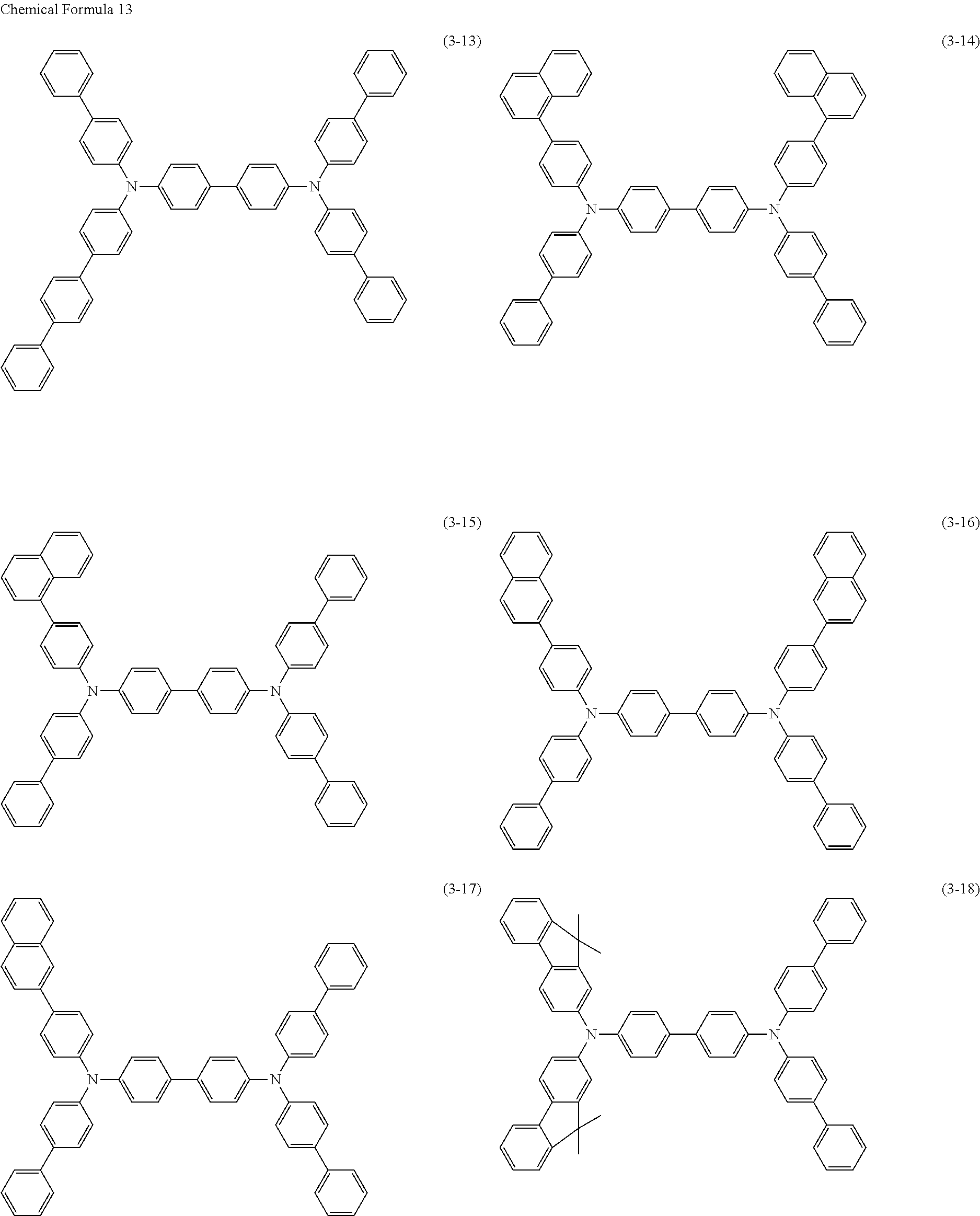
- Specific examples of a compound represented by the formula (3) include compounds represented by the following formulas (3-1) to (3-45).
- the hole transport layers 16 BB of the blue organic EL elements 10 B are provided to enhance hole transport efficiency to the blue light-emitting layer 16 CB, and are arranged on the hole injection layers 16 AB, respectively.
- the thickness of each hole transport layer 16 BB is preferably within a range of 10 nm to 200 nm both inclusive, and more preferably 15 nm to 150 nm both inclusive.
- the hole transport layers 16 BB include at least a low-molecular material. Therefore, in the organic EL display, improvements in blue light emission efficiency and lifetime are achievable. Moreover, as in the case of the low-molecular material added to the red light-emitting layers 16 CR and the green light-emitting layers 16 CG, the low-molecular material used herein is a low-molecular material with a single molecular weight except for a compound such as a polymer or a condensation product of a low-molecular compound, and the low-molecular material is present in a single molecular form.
- the low-molecular material used in the hole transport layers 16 BB for example, benzine, styrylamine, triphenylamine, porphyrin, triphenylene, azatriphenylene, tetracyanoquinodimethane, triazole, imidazole, oxadiazole, polyarylalkane, phenylenediamine, arylamine, oxazole, anthracene, fluorenone, hydrazone, stilbene or a derivative thereof, or a heterocyclic conjugated monomer, oligomer or polymer such as a polysilane-based compound, vinylcarbazole-based compound, an thiophene-based compound or an aniline-based compound is allowed to be used.
- the hole transport layers 16 BB are preferably formed with use of any of the low-molecular materials represented by the above-described formulas (1) to (3), and specific examples include compounds represented by the above-described formulas (1-1) to (1-48), (2-1) to (2-69) and (3-1) to (3-45).
- the blue light-emitting layer 16 CB emits light by the recombination of electrons and holes in response to the application of an electric field, and the blue-light emitting layer 16 CB is arranged as a common layer on whole surfaces of the red light-emitting layers 16 CR, the green light-emitting layers 16 CG and the hole transport layers 16 BB for the blue organic EL elements 10 B.
- the blue light-emitting layer 16 CB includes an anthracene compound as a host material doped with a blue or green fluorescent pigment as a guest material to emit blue or green light.
- a compound represented by a formula (4) is preferably used as the host material forming the blue light-emitting layer 16 CB.
- R1 to R6 each are a hydrogen atom, a halogen atom, a hydroxyl group, a cyano group, a nitro group, or a group including a carbonyl group with 20 or less carbon atoms, a group including a carbonyl ester group, an alkyl group, an alkenyl group, an alkoxyl group, a group including a silyl group with 30 or less carbon atoms, a group including an aryl group, a group including a heterocyclic group, a group including an amino group, or a derivative thereof.
- Examples of the group including an aryl group indicated by R1 to R6 in the compound represented by the formula (4) include a phenyl group, a 1-naphthyl group, a 2-naphthyl group, a fluorenyl group, a 1-anthryl group, a 2-anthryl group, a 9-anthryl group, a 1-phenanthryl group, a 2-phenanthryl group, a 3-phenanthryl group, a 4-phenanthryl group, a 9-phenanthryl group, a 1-naphthacenyl group, a 2-naphthacenyl group, a 9-naphthacenyl group, a 1-pyrenyl group, a 2-pyrenyl group, a 4-pyrenyl group, a 1-chrysenyl group, a 6-chrysenyl group, a 2-fluoranthenyl group, a 3-fluoranthenyl group,
- the group including a hetereocyclic group indicated by R1 to R6 is a five- or six-membered ring aromatic ring group containing an oxygen atom (O), a nitrogen atom (N) and a sulfur atom (S) as hetero atoms, or a condensed polycyclic aromatic ring group with 2 to 20 carbon atoms.
- a heterocyclic group include a thienyl group, a furyl group, a pyrrolyl group, a pyridyl group, a quinolyl group, a quinoxalyl group, an imidazopyridyl group and a benzothiazole group.
- Representative examples include a 1-pyrrolyl group, a 2-pyrrolyl group, a 3-pyrrolyl group, a pyrazinyl group, a 2-pyridinyl group, a 3-pyridinyl group, a 4-pyridinyl group, a 1-indolyl group, a 2-indolyl group, a 3-indolyl group, a 4-indolyl group, a 5-indolyl group, a 6-indolyl group, a 7-indolyl group, a 1-isoindolyl group, a 2-isoindolyl group, a 3-isoindolyl group, a 4-isoindolyl group, a 5-isoindolyl group, a 6-isoindolyl group, a 7-isoindolyl group, a 2-furyl group, a 3-furyl group, a 2-benzofuranyl group, a
- the group including an amino group indicated by R1 to R6 may be any one of an alkylamino group, an arylamino group, an aralkylamino group and the like. They preferably include an aliphatic hydrocarbon group with 1 to 6 carbon atoms and/or an aromatic ring group with 1 to 4 carbon atoms. Such groups include a dimethylamino group, a diethylamino group, a dibutylamino group, a diphenylamino group, a ditolylamino group, a bisbiphenylylamino group and a dinaphthylamino group. Note that the above-described substituent group may form a condensed ring configured of two or more substituent groups, and further, the above-described substituent group may be a derivative thereof.
- a luminescent guest material forming the blue light-emitting layer 16 CB for example, an organic light-emitting material such as a low-molecular fluorescent material, a phosphorescent dye or a metal complex is used.
- a blue luminescent guest material herein indicates a compound having a peak in a light emission wavelength range of approximately 400 nm to 490 nm.
- an organic material such as a naphthalene derivative, an anthracene derivative, a naphthacene derivative, a styrylamine derivative or a bis(azinyl)methene boron complex is used.
- the compound it is preferable to select one from the group consisting of an aminonaphthalene derivative, an aminoanthracene derivative, an aminochrysene derivative, an aminopyrene derivative, a styrylamine derivative and a bis(azinyl)methene boron complex.
- the electron transport layer 16 D is provided to enhance electron transport efficiency to the red light-emitting layers 16 CR, the green light-emitting layers 16 CG and the blue light-emitting layer 16 CB, and is arranged on a whole surface of the blue light-emitting layer 16 CB as a common layer.
- Examples of the material of the electron transport layer 16 D include quinoline, perylene, phenanthroline, bisstyryl, pyrazine, triazole, oxazole, fullerene, oxadiazole, fluorenone, a derivative thereof and a metal complex thereof.
- tris(8-hydroxyquinoline)aluminum Alq3 for short
- anthracene naphthalene
- phenanthrene pyrene
- anthracene perylene
- butadiene coumarin
- C60 acridine
- stilbene 1,10-phenanthroline
- a derivative thereof or a metal complex thereof is used.
- the electron injection layer 16 E is provided to enhance electron injection efficiency, and is arranged on a whole surface of the electron transport layer 16 D.
- As the material of the electron injection layer 16 E lithium oxide (Li 2 O) which is an oxide of lithium (Li), cesium carbonate (Cs 2 CO 3 ) which is a complex oxide of cesium (Cs), or a mixture of the oxide and the complex oxide may be used.
- the material of the electron injection layer 16 E is not limited thereto, and, for example, an alkali-earth metal such as calcium (Ca) or barium (Ba), an alkali metal such as lithium or cesium, and further a metal with a small work function such as indium (In) or magnesium (Mg), or an oxide, a complex oxide or a fluoride of any of these metals may be used singly, or a mixture or an alloy thereof for improving stability may be used.
- an alkali-earth metal such as calcium (Ca) or barium (Ba)
- an alkali metal such as lithium or cesium
- a metal with a small work function such as indium (In) or magnesium (Mg)
- an oxide, a complex oxide or a fluoride of any of these metals may be used singly, or a mixture or an alloy thereof for improving stability may be used.
- the upper electrode 17 has, for example, a thickness of 2 nm to 15 nm both inclusive, and is configured of a metal conductive film. More specifically, an alloy of Al, Mg, Ca or Na is used. In particular, an alloy of magnesium and silver (an Mg—Ag alloy) is preferable, because the Mg—Ag alloy has both of electrical conductivity and small absorption in a thin film.
- the material of the upper electrode 17 may be an alloy of Al and Li (an Al—Li alloy).
- the upper electrode 17 may be configured of a mixture layer including an organic light-emitting material such as an aluminum quinoline complex, a styrylamine derivative or a phthalocyanine derivative.
- the upper electrode 17 may further include a layer including light transmittance such as MgAg. Note that in the case of an active matrix drive system, the upper electrode 17 is formed on the whole substrate 11 so as to be insulated from the lower electrodes 14 by the organic layer 16 and the barrier rib 15 , and is used as a common electrode for the red organic EL elements 10 R, the green organic EL elements 10 G and the blue organic EL elements 10 B.
- the protective layer 20 has, for example, a thickness of 2 to 3 ⁇ m both inclusive, and may be made of an insulating material or a conductive material.
- an organic amorphous insulating material for example, amorphous silicon ( ⁇ -Si), amorphous silicon carbide ( ⁇ -SiC), amorphous silicon nitride ( ⁇ -Si 1-x N x ), amorphous carbon ( ⁇ -C) or the like is preferable.
- ⁇ -Si amorphous silicon
- ⁇ -SiC amorphous silicon carbide
- ⁇ -Si 1-x N x amorphous silicon nitride
- ⁇ -C amorphous carbon
- the sealing substrate 40 is arranged on a side close to the upper electrode 17 of the red organic EL elements 10 R, the green organic EL elements 10 G and the blue organic EL elements 10 B, and is provided to seal the red organic EL elements 10 R, the green organic EL elements 10 G and the blue organic El elements 10 B with an adhesive layer (not illustrated).
- the sealing substrate 40 is made of a transparent material to light emitted from the red organic EL elements 10 R, the green organic EL elements 10 G and the blue organic EL elements 10 B such as glass.
- a color filter and a light-shielding film as a black matrix are arranged to extract light emitted from the red organic EL elements 10 R, the green organic EL elements 10 G and the blue organic EL elements 10 B and absorb outside light reflected from the red organic EL elements 10 R, the green organic EL elements 10 G and the blue organic EL elements 10 B and wiring therebetween, thereby improving contrast.
- the color filter includes red filters, green filters and blue filters (all not illustrated) which are arranged in order so as to correspond to the red organic EL elements 10 R, the green organic EL elements 10 G and the blue organic EL elements 10 B, respectively.
- the red filters, the green filters and the blue filters have, for example, a rectangular shape, and are formed without space.
- the red filters, the green filters and the blue filters are made of a resin mixed with a pigment of a corresponding color, and are adjusted by selecting the pigment so that light transmittance in a target red, green or blue wavelength range is high and light transmittance in other wavelength ranges is low.
- the wavelength range with high transmittance in the color filter and a peak wavelength ⁇ of a spectrum of light to be extracted from a resonator configuration are equal to each other. Therefore, only light of a wavelength equal to the peak wavelength ⁇ of the spectrum of light to be extracted in outside light entering from the sealing substrate 40 passes through the color filter, and outside light of other wavelengths is prevented from entering into the red, green and blue organic EL elements 10 R, 10 G and 10 B.
- the light-shielding film is configured of, for example, a black resin film mixed with a black colorant with an optical density of 1 or over, or a thin-film filter utilizing interference of a thin film.
- the light-shielding film is preferably configured of the black resin film, because the light-shielding film is easily formed at low cost.
- the thin-film filter is formed, for example, by laminating one or more thin films made of metal, a metal nitride or a metal oxide, and utilizes interference of the thin film to attenuate light. More specifically, as the thin-film filter, a thin-film filter formed by alternately laminating chromium and chromium (III) oxide (Cr 2 O 3 ) is used.
- the organic EL display is allowed to be manufactured by, for example, the following steps.
- FIG. 4 illustrates a flow of a method of manufacturing the organic EL display
- FIGS. 5A to 5C to FIGS. 7A to 7C illustrate the manufacturing method illustrated in FIG. 4 in order of steps.
- the pixel drive circuit 140 including the driving transistor Tr 1 is formed on the substrate 11 made of the above-described material, and, for example, an planarization insulating film (not illustrated) made of a photosensitive resin is arranged.
- a transparent conductive film made of ITO is formed on a whole surface of the substrate 11 , and the transparent conductive film is patterned to form the lower electrodes 14 for the red organic EL elements 10 R, the green organic EL elements 10 G and the blue organic EL elements 10 B, respectively, as illustrated in FIG. 5A (step S 101 ).
- the lower electrodes 14 each are electrically connected to a drain electrode of the driving transistor Tr 1 through a contact hole (not illustrated) of the planarization insulating film (not illustrated).
- a film made of an inorganic insulating material such as SiO 2 is formed on the lower electrodes 14 and the planarization insulating film (not illustrated) by, for example, a CVD (Chemical Vapor Deposition) method, and is patterned with use of a photolithography technique and an etching technique to form the lower barrier rib 15 A.
- CVD Chemical Vapor Deposition
- the upper barrier rib 15 B made of the above-described photosensitive resin is formed in a predetermined position of the lower barrier rib 15 A, more specifically a position around a light emission region of each pixel. Therefore, the barrier rib 15 including the upper barrier rib 15 A and the lower barrier rib 15 B is formed (step S 102 ).
- a surface where the lower electrodes 14 and the barrier rib 15 are formed of the substrate 11 is subjected to oxygen plasma treatment to remove a contaminant such as an organic matter adhered to the surface, thereby improving wettability. More specifically, the substrate 11 is heated at a predetermined temperature, for example, approximately 70 to 80° C., and then is subjected to plasma treatment (O 2 plasma treatment) using oxygen as a reactive gas under atmospheric pressure.
- oxygen plasma treatment oxygen plasma treatment
- water repellent treatment liquid repellent treatment
- step S 103 water repellent treatment (liquid repellent treatment) is performed so as to reduce wettabilitiy of specifically a top surface and a side surface of the upper barrier rib 15 B. More specifically, plasma treatment (CF 4 plasma treatment) using tetrafluoromethane as a reactive gas is performed under atmospheric pressure, and after that, the substrate 11 heated for the plasma treatment is cooled to a room temperature so as to make the top surface and the side surface of the upper barrier rib 15 B liquid-repellent, thereby reducing wattability thereof.
- plasma treatment CF 4 plasma treatment
- tetrafluoromethane as a reactive gas
- the hole injection layers 16 AR, 16 AG and 16 AB made of the above-described material are formed in regions surrounded by the upper barrier rib 15 B (step S 104 ).
- the hole injection layers 16 AR, 16 AG and 16 AB are formed by a coating method such as a spin coating method or a liquid droplet discharging method.
- a coating method such as a spin coating method or a liquid droplet discharging method.
- an ink-jet printing method which is the liquid droplet discharging method, or a nozzle coating method is preferably used.
- a solution or a dispersion liquid such as polyaniline or polythiophene which is the forming material of the hole injection layers 16 AR, 16 AG and 16 AB is discharged to the exposed surfaces of the lower electrodes 14 by, for example, the ink jetprinting method. After that, heat treatment (drying treatment) is performed to form the hole injection layers 16 AR, 16 AG and 16 AB.
- a solvent or a dispersion medium is dried, and then heated at high temperature.
- the heat treatment is preferably performed in an air or oxygen atmosphere, because electrical conductivity is easily developed by oxidation of the conductive high polymer by oxygen.
- the heating temperature is preferably within a range of 150° C. to 300° C. both inclusive, and more preferably within a range of 180° C. to 250° C. both inclusive.
- the heating time is preferably within a range of approximately 5 minutes to 300 minutes, and more preferably within a range of 10 minutes to 240 minutes both inclusive.
- the thickness of a dried film is preferably within a range of 5 nm to 100 nm both inclusive, and more preferably within a range of 8 nm to 50 nm both inclusive.
- the hole transport layers 16 BR and 16 BG made of the above-described material are formed on the hole injection layers 16 AR and 16 AG of the red organic EL elements 10 R and the green organic EL elements 10 G, respectively (step S 105 ).
- the hole transport layers 16 BR and 16 BG are formed by a coating method such as a spin coating method or a liquid droplet discharging method.
- the ink-jet printing method which is the liquid droplet discharging method, or the nozzle coating method is preferably used.
- a solution or a dispersion liquid of a high polymer which is the forming material of the hole transport layers 16 BR and 16 BG is discharged to exposed surfaces of the hole injection layers 16 AR and 16 AG by, for example, a ink-jet printing method. After that, heat treatment (drying treatment) is performed to form the hole transport layers 16 BR and 16 BG of the red organic EL elements 10 R and the green organic EL elements 10 G.
- a solvent or a dispersion liquid is dried, and then heated at high temperature.
- an atmosphere for coating or an atmosphere for drying and heating the solvent an atmosphere including nitrogen (N 2 ) as a main component is preferable, because when oxygen or water is included in the atmosphere, the light emission efficiency or lifetime of the formed organic EL display may be reduced.
- N 2 nitrogen
- the oxygen concentration is preferably within a range of 0.1 ppm to 100 ppm both inclusive, and more preferably within a range of 50 ppm or less.
- the oxygen concentration is larger than 100 ppm, an interface of a formed thin film may be contaminated to reduce the light emission efficiency and lifetime of the obtained organic EL display.
- the oxygen concentration is smaller than 0.1 ppm, such a low concentration does not cause an issue in properties of the elements, but in a present mass-production process, the cost of an apparatus for maintaining an atmosphere with an oxygen concentration of smaller than 0.1 ppm may be high.
- the dew point of water is preferably within a range of, for example, ⁇ 80° C. to ⁇ 40° C. both inclusive, more preferably ⁇ 50° C. or less, and more preferably ⁇ 60° C. or less.
- ⁇ 40° C. When water with a dew point of higher than ⁇ 40° C. is present, an interface of a formed thin film may be contaminated to reduce the light emission efficiency or lifetime of the obtained organic EL display.
- water with a dew point of lower than ⁇ 80° C. such a low temperature does not cause the properties of the elements, but as a present mass-production process, the cost of an apparatus for keeping an atmosphere at lower than ⁇ 80° C. may be high.
- the heating temperature is preferably within a range of 100° C. to 230° C. both inclusive, and more preferably within a range of 100° C. to 200° C. both inclusive. At least the heating temperature is preferably lower than a temperature for forming the hole injection layers 16 AR, 16 AG and 16 AB.
- the heating time depending on temperature or atmosphere, is preferably within a range of approximately 5 minutes to 300 minutes, and more preferably within a range of 10 minutes to 240 minutes both inclusive.
- the thickness of a dried film is preferably within a range of 10 nm to 200 nm both inclusive and more preferably within a range of 15 nm to 150 nm both inclusive.
- the red light-emitting layers 16 CR made of a mixture material of the above-described high-molecular material and the above-described low-molecular material are formed on the hole transport layers 16 BR of the red organic EL elements 10 R.
- the green light-emitting layers 16 CG made of a mixture material of the above-described high-molecular material and the above-described low-molecular material are formed on the hole transport layers 16 BG of the green organic EL elements 10 G (step S 106 ).
- the red light-emitting layers 16 CR and the green light-emitting layers 16 CG are formed by a coating method such as a spin coating method or a liquid droplet discharging method.
- a coating method such as a spin coating method or a liquid droplet discharging method.
- the ink-jet printing method which is the liquid droplet discharging method, or the nozzle coating method is preferably used.
- a solution or a dispersion liquid of a high polymer which is the forming material of the red light-emitting layers 16 CR or the green light-emitting layers 16 CG is discharged on exposed surfaces of the hole transport layers 16 BR or 16 BG by, for example, the ink-jet printing method.
- heat treatment by the same method under the same conditions as in the heat treatment (drying treatment) described in the step of forming the hole transport layers 16 BR and 16 BG of the above-described red organic EL elements 10 R and the above-described green organic EL elements 10 G is performed to form the red light-emitting layers 16 BR and the green light-emitting layers 16 BG.
- the hole transport layers 16 BB made of the above-described low-molecular material is formed on the hole injection layers 16 AB for the blue organic EL elements 10 B (step S 107 ).
- the hole transport layers 16 BB are formed by a coating method such as a spin coating method or a liquid droplet discharging method.
- the ink-jet printing method which is the liquid droplet discharging method, or the nozzle coating method is preferably used.
- a solution or a dispersion liquid of the low-molecular material which is the forming material of the hole transport layers 16 BB is discharged on exposed surfaces of the hole injection layers 16 AB by, for example, the ink jet printing method.
- heat treatment by the same method under the same conditions as in the heat treatment (drying treatment) described in the step of forming the hole transport layers 16 BR and 16 BG of the above-described red organic EL elements 10 R and the above-described green organic EL elements 10 G is performed to form the hole transport layers 16 BB.
- the step of forming the hole transport layers 16 BR and 16 BG of the red organic EL elements 10 R and the green organic EL elements 10 G, the step of forming the hole transport layers 16 BB of the blue organic EL elements 10 B, and the step of forming the red light-emitting layers 16 CR and the green light-emitting layers 16 CG may be performed in any order, but it is necessary to previously form a base where layers to be formed are developed and to undergo a heating step in each heating and drying step. Moreover, it is necessary to perform coating at a temperature in the heating step equal to or lower than a temperature in a previous step.
- coating may be performed to form the red light-emitting layers 16 CR and the green light-emitting layers 16 CG, and then without drying the red light-emitting layers 16 CR and the green light-emitting layers 16 CG, coating may be performed to form the hole transport layers 16 BB of the blue organic EL elements 10 B, and after that, the step of drying and heating the red light-emitting layers 16 CR, the green light-emitting layers 16 CG and the hole transport layers 16 BB of the blue organic EL elements 10 B may be performed.
- the drying step and the heating step are preferably performed separately, because in the drying step, a coated wet film easily flows, thereby easily forming the film uneven.
- a preferable drying step is a method of uniformly drying a film in a vacuum at normal pressure, and more preferably, the film is dried with keeping wind off the film.
- a solvent is removed to some extent to reduce fluidity, and the film is hardened. Then, when the film is slowly heated, a small amount of the remaining solvent is allowed to be removed, or the light-emitting material or the material of the hole transport layer is allowed to be rearranged at a molecular level.
- the blue light-emitting layer 16 CB made of the above-described low-molecular material is formed as a common layer on the whole surfaces of the red light-emitting layers 16 CR, the green light-emitting layers 16 CG and the hole transport layers 16 BB of the blue organic EL elements 10 B (step S 108 ).
- the electron transport layer 16 D, the electron injection layer 16 E and the upper electrode 17 made of the above-described materials are formed by an evaporation method on a whole surface of the blue light-emitting layer 16 CB (step S 109 , S 110 and S 111 ).
- the protective layer 20 is formed by a film formation method with small energy of film formation particles, for example, an evaporation method or a CVD method so as not to exert an influence on the base.
- a film formation method with small energy of film formation particles for example, an evaporation method or a CVD method so as not to exert an influence on the base.
- the protective layer 20 is formed by the CVD method so as to have a thickness of 2 to 3 ⁇ m both inclusive.
- the film formation temperature is set to room temperature and a film is formed under a condition in which stress on the film is minimized to prevent peeling of the protective layer 20 .
- the blue light-emitting layer 16 CB, the electron transport layer 16 D, the electron injection layer 16 E, the upper electrode 17 and the protective layer 20 are formed on a whole surface without using a mask. Moreover, the blue light-emitting layer 16 CB, the electron transport layer 16 D, the electron injection layer 16 E, the upper electrode 17 and the protective layer 20 are preferably formed sequentially in one and the same film formation apparatus without being exposed to air. Therefore, deterioration in the organic layer 16 due to water in air is preventable.
- the organic layer 16 formed on a whole top surface of the auxiliary electrode may be removed by a technique such as laser ablation before forming the upper electrode 17 . Therefore, the upper electrode 17 is allowed to be directly connected to the auxiliary electrode, thereby improving contact.
- the light-shielding film made of the above-described material is formed on the sealing substrate 40 made of the above-described material.
- the sealing substrate 40 is coated with the material of the red filter (not illustrated) by spin coating or the like, and the material is patterned by a photolithography technique and fired to form the red filter.
- the blue filter and the green filter are formed in order.
- the adhesive layer (not illustrated) is formed on the protective layer 20 , and the sealing substrate 40 is bonded to the protective layer 20 with the adhesive layer in between.
- the display illustrated in FIGS. 1 to 3 is completed.
- a scanning signal is supplied from the scanning line drive circuit 130 to each pixel through a gate electrode of the writing transistor Tr 2 , and an image signal supplied from the signal line drive circuit 120 through the writing transistor Tr 2 is retained in the retention capacitor Cs.
- on/off control of the driving transistor Tr 1 is performed in response to the signal retained in the retention capacitor Cs, and a drive current Id is thereby injected into each of the red organic EL elements 10 R, the green organic EL elements 10 G and the blue organic EL elements 10 B to emit light by the recombination of electrons and holes.
- the light passes through the lower electrodes 14 and the substrate 11
- the light passes through the upper electrode 17 , the color filter (not illustrated) and the sealing substrate 40 , and then the light is extracted.
- each red organic EL element 10 R the red light-emitting layer 16 CR and the blue light-emitting layer 16 CB are arranged, but energy is transferred to red with a lowest energy level to predominantly emit red light.
- the green organic EL element 10 G the green light-emitting layer 16 CG and the blue light-emitting layer 16 CB are arranged, but energy is transferred to green with a lower energy level to predominantly emit green light.
- each blue organic EL element 10 B only the blue light-emitting layer 16 CB is included, so blue light is emitted.
- the red light-emitting layer 16 CR and the green light-emitting layer 16 CG are made of the high-molecular material to which the low-molecular material is added, so a difference between the energy levels of the red light-emitting layers 16 CR and the green light-emitting layers 16 CG and the energy level of the blue light-emitting layer 16 CB made of the low-molecular material is reduced.
- the hole or electron injection efficiency from the blue light-emitting layer 16 CB to the red light-emitting layers 16 CR or the green light-emitting layers 16 CG is improved, and a value close to element properties of the red light-emitting layers 16 CR and the green light-emitting layers 16 CG is allowed to be actually obtained.
- the red light-emitting layers 16 CR and the green light-emitting layers 16 CG are formed by a coating method with use of a mixture material of the high-molecular material and the low-molecular material, so hole or electron transport efficiency from the blue light-emitting layer 16 CB to the red light-emitting layers 16 CR or the green light-emitting layers 16 CG is improved, and a value close to the element properties of the red light-emitting layers 16 CR and the green light-emitting layers 16 CG is obtained.
- higher light emission efficiency and a longer lifetime of the color organic EL display configured by forming the red organic EL elements 10 R, the green organic EL elements 10 G and the blue organic EL elements 10 B in an array are achievable.
- the organic EL display according to the above-described embodiment is applicable to displays of electronic devices displaying a picture signal supplied from outside or a picture signal produced inside as an image or a picture in any fields, such as televisions, digital cameras, notebook personal computers, portable terminal devices such as cellular phones, and video cameras.
- the organic EL display according to the above-described embodiment is incorporated into various electronic devices such as Application Examples 1 to 5 which will be described later as a module as illustrated in FIG. 8 .
- a region 210 exposed from the protective layer 20 and the sealing substrate 40 is arranged on a side of the substrate 11 , and an external connection terminal (not illustrated) is formed in the exposed region 210 by extending the wiring of the signal line drive circuit 120 and the scanning line drive circuit 130 .
- a flexible printed circuit (FPC) 220 for signal input/output may be arranged.
- FIG. 9 illustrates an appearance of a television to which the organic EL display according to the above-described embodiment is applied.
- the television has, for example, a picture display screen section 300 including a front panel 310 and a filter glass 320 , and the picture display screen section 300 is configured of the organic EL display according to the above-described embodiment.
- FIGS. 10A and 10B illustrate an appearance of a digital camera to which the organic EL display according to the above-described embodiment is applied.
- the digital camera has, for example, a light-emitting section for a flash 410 , a display section 420 , a menu switch 430 and a shutter button 440 , and the display section 420 is configured of the organic EL display according to the above-described embodiment.
- FIG. 11 illustrates an appearance of a notebook personal computer to which the organic EL display according to the above-described embodiment is applied.
- the notebook personal computer has, for example, a main body 510 , a keyboard 520 for operation of inputting characters and the like and a display section 530 for displaying an image, and the display section 530 is configured of the organic EL display according to the above-described embodiment.
- FIG. 12 illustrates an appearance of a video camera to which the organic EL display according to the above-described embodiment is applied.
- the video camera has, for example, a main body 610 , a lens for shooting an object 620 arranged on a front surface of the main body 610 , a shooting start/stop switch 630 and a display section 640 , and the display section 640 is configured of the organic EL display according to the above-described embodiment.
- FIGS. 13A to 13G illustrate an appearance of a cellular phone to which the organic EL display according to the above-described embodiment is applied.
- the cellular phone is formed by connecting, for example, a top-side enclosure 710 and a bottom-side enclosure 720 to each other by a connection section (hinge section) 730 .
- the cellular phone has a display 740 , a sub-display 750 , a picture light 760 , and a camera 770 .
- the display 740 or the sub-display 750 is configured of the organic EL display according to the above-described embodiment.
- the red organic EL elements 10 R, the green organic EL element 10 G and the blue organic EL element 10 B were formed on the substrate 11 with a size of 25 mm ⁇ 25 mm.
- a glass substrate (25 mm ⁇ 25 mm) was prepared as the substrate 11 , and two-layer configurations including a silver alloy layer made of an Ag—Pd—Cu alloy with a thickness of 120 nm and a transparent conductive film made of ITO with a thickness of 10 nm were formed as the lower electrodes 14 on the substrate 11 (step S 101 ).
- step S 104 coating with ND1501 (polyaniline manufactured from Nissan Chemical Industries. Ltd.) was performed in air by a spin coating method to form the hole injection layers 16 AR, 16 AG and 16 AB with a thickness of 15 nm, and then the hole injection layers 16 AR, 16 AG and 16 AB were thermally cured on a hot plate at 220° C. for 30 minutes (step S 104 ).
- ND1501 polyaniline manufactured from Nissan Chemical Industries. Ltd.
- the polymer (polyvinylcarbazole) represented by a formula (5) was applied to the hole injection layers 16 AR and 16 AG by a spin coating method to form the hole transport layers 16 BR and 16 BG.
- the hole transport layer 16 BR of each red organic EL element 10 R had a thickness of 150 nm
- the hole transport layer 16 BG of each green organic EL element 10 G had a thickness of 20 nm.
- the hole transport layers 16 BR and 16 BG were thermally cured on a hot plate at 180° C. for 60 minutes (step S 105 ).
- a mixture material formed by mixing a fluorenone-based polyarylene material having benzothiadiazole in a block with the low-molecular material represented by the formula (2-38) at a weight ratio of 2:1 was dissolved in xylene, and the mixture material was applied to the hole transport layers 10 BR of the red organic EL elements 10 R by a spin coating method to form layers with a thickness of 80 nm as the red light-emitting layers 16 CR (Experimental Example 1-1).
- a mixture material formed by mixing a fluorenone-based polyarylene material having anthracene in a block with the low-molecular material represented by the formula (2-38) at a weight ratio of 2:1 was dissolved in xylene, and the mixture material was applied to the hole transport layers 16 BG of the green organic EL elements 10 G by a spin coating method to form layers with a thickness of 80 nm as the green light-emitting layers 16 CG (Experimental Example 2-1).
- the red light-emitting layers 16 CR and the green light-emitting layers 16 CG were thermally cured on a hot plate at 130° C. for 10 minutes (step S 106 ).
- the low-molecular material represented by the formula (2-38) was applied to the hole injection layers 16 AB of the blue organic EL elements 10 B by a spin coating method to form layer with a thickness of 50 nm as the hole transport layers 16 BB (Experimental Example 3-1). After that, in a N 2 atmosphere (with a dew point of ⁇ 60° C. and an oxygen concentration of 10 ppm), the hole transport layers 16 BB was heated on a hot plate at 100° C. for 60 minutes (step S 107 ).
- the substrate 11 for the red organic EL elements 10 R in which layers until the red light-emitting layers 16 CR were formed, and the substrate 11 for the green organic EL elements 10 G in which layers until the green light-emitting layers 16 CG were formed, and the substrate 11 for the blue organic EL elements in which layers until the hole transport layers 16 BB were formed were put into a vacuum deposition apparatus to evaporate the blue light-emitting layers 16 CB and subsequent layers.
- ADN (9,10-di(2-naphthyl)anthracene represented by the formula (4-20) and a blue dopant represented by a formula (6) were co-evaporated at a weight ratio of 95:5 (step S 108 ).
- Alq3 tris(8-hydroxyquinoline)aluminum represented by a formula (7) was evaporated by a vacuum deposition method to form a layer with a thickness of 15 nm as the electron transport layer 16 D (step S 109 ).
- a film of LiF with a thickness of 0.3 nm was formed as the electron injection layer 16 E by the same evaporation method (step S 110 ), and then a layer of Mg—Ag with a thickness of 10 nm was formed as the upper electrode 17 (step S 111 ).
- the protective layer 20 made of SiN was formed by a CVD method, and a transparent resin was used to perform solid sealing.
- a full-color organic EL display was obtained by combining the red organic EL elements 10 R, the green organic EL elements 10 G and the blue organic El elements 10 B which were obtained in such a manner.
- the compound represented by the formula (2-38) was replaced with low-molecular materials represented by the following formula (8), and the formulas (2-6), (2-24), (2-39), (3-5), (3-10), (1-29) and (1-34) so as to prepare the red organic EL elements 10 R (Experimental Examples 1-2 to 1-9) and green organic EL elements 10 G (Experimental Examples 2-2 to 2-9), and a red organic EL element (Experimental Example 1-10) in which the low-molecular material was not added and a green organic EL element (Experimental Example 2-10) in which the low-molecular material was not added were prepared.
- FIGS. 14A to 14C are plots illustrating the results of the drive voltage (V) ( FIG. 14A ), the light emission efficiency (cd/A) ( FIG. 14B ) and the luminance half time ( FIG. 14C ) in the case of constant-current driving at a current density of 100 mA/cm 2 of Experimental Example 1-1 and Experimental Example 1-10 in which the low-molecular material was not added to the red light-emitting layer 16 CR.
- FIGS. 15A and 15B are plots illustrating results of the light emission efficiency (cd/A) ( FIG. 15A ) and the luminance half time ( FIG. 15B ) in the case of constant-current driving at a current density of 100 mA/cm 2 of Experimental Example 2-1 and Experimental Example 2-10 in which the low-molecular material was not added to the green light-emitting layer 16 CG.
- the additive amount of the low-molecular material (represented by the formula (2-38)) added to the high-molecular material was changed to 0%, 11%, 20%, 25%, 33%, 50%, 66% and 80% to measure changes in luminance half time in the case of constant-current driving at a current density of 100 mA/cm 2 .
- Table 4 illustrates results of the additive amount of the low-molecular material and the luminance half time in Experiment 2.
- FIG. 16 illustrates a plot of the results of Experiment 2. It was obvious from Table 4 and FIG. 16 that when the low-molecular material was added to the high-molecular material forming the light-emitting layer 16 C, the luminance half time of the organic EL element 10 R was improved, and when the additive amount was preferably within a range of 10% to 70% both inclusive, the luminance half time was allowed to be effectively improved. In particular, when the additive amount was approximately 30%, the luminance half time was allowed to be remarkably improved.
- each layer the material and thickness of each layer, the method and conditions of forming each layer are not limited to those described in the above-described embodiment and the above-described examples, and each layer may be made of any other material with any other thickness by any other method under any other conditions.
- the configurations of the organic EL elements 10 R, 10 B and 10 G are specifically described; however, all layers are not necessarily included, or any other layer may be further included.
- the case of the active matrix display was described.
- the invention is applicable to a passive matrix display.
- the configuration of a pixel drive circuit for active matrix drive is not limited to that described in the above-described embodiment, and if necessary, a capacitive element or a transistor may be added.
- a necessary drive circuit may be included in addition to the above-described signal line drive circuit 120 and the scanning line drive circuit 130 according to a change in the pixel drive circuit.
Landscapes
- Physics & Mathematics (AREA)
- Spectroscopy & Molecular Physics (AREA)
- Chemical & Material Sciences (AREA)
- Engineering & Computer Science (AREA)
- Materials Engineering (AREA)
- Optics & Photonics (AREA)
- Electroluminescent Light Sources (AREA)
Abstract
Description


| TABLE 1 | |||||||
| Mixture ratio | |||||||
| (high- | |||||||
| molecular | Light | ||||||
| material:low- | Drive | emission | Lifetime | ||||
| molecular | voltage | efficiency | (Luminance | ||||
| Red light-emitting layer | material | (V) | (cd/A) | Chromaticity | half time/h) | ||
| Experimental | High-molecular material/ | 2:1 | 7.1 | 8.4 | 0.67 0.32 | 200 |
| Example 1-1 | Formula (2-38) | |||||
| Experimental | High-molecular material/ | 2:1 | 7.3 | 8.2 | 0.67 0.32 | 190 |
| Example 1-2 | Formula (8) | |||||
| Experimental | High-molecular material/ | 2:1 | 7.5 | 8.0 | 0.67 0.32 | 170 |
| Example 1-3 | Formula (2-6) | |||||
| Experimental | High-molecular material/ | 2:1 | 7.7 | 7.8 | 0.67 0.32 | 160 |
| Example 1-4 | Formula (2-24) | |||||
| Experimental | High-molecular material/ | 2:1 | 7.2 | 7.6 | 0.67 0.32 | 170 |
| Example 1-5 | Formula (2-39) | |||||
| Experimental | High-molecular material/ | 2:1 | 7.2 | 8.3 | 0.67 0.32 | 185 |
| Example 1-6 | Formula (3-5) | |||||
| Experimental | High-molecular material/ | 2:1 | 8.3 | 7.4 | 0.67 0.32 | 140 |
| Example 1-7 | Formula (3-10) | |||||
| Experimental | High-molecular material/ | 2:1 | 8.5 | 7.8 | 0.67 0.32 | 155 |
| Example 1-8 | Formula (1-29) | |||||
| Experimental | High-molecular material/ | 2:1 | 8.7 | 7.6 | 0.67 0.32 | 150 |
| Example 1-9 | Formula (1-34) | |||||
| Experimental | High-molecular material/— | 2:1 | 9.0 | 6.7 | 0.67 0.32 | 10 |
| Example 1-10 | ||||||
| TABLE 2 | |||||||
| Mixture ratio | |||||||
| (high- | |||||||
| molecular | Light | ||||||
| material:low- | Drive | emission | Lifetime | ||||
| molecular | voltage | efficiency | (Luminance | ||||
| Green light-emitting layer | material | (V) | (cd/A) | Chromaticity | half time/h) | ||
| Experimental | High-molecular material/ | 2:1 | 4.8 | 17.0 | 0.26 0.65 | 300 |
| Example 2-1 | Formula (2-38) | |||||
| Experimental | High-molecular material/ | 2:1 | 4.9 | 16.5 | 0.26 0.65 | 280 |
| Example 2-2 | Formula (8) | |||||
| Experimental | High-molecular material/ | 2:1 | 5.2 | 13.2 | 0.26 0.65 | 270 |
| Example 2-3 | Formula (2-6) | |||||
| Experimental | High-molecular material/ | 2:1 | 5.3 | 14.5 | 0.26 0.65 | 265 |
| Example 2-4 | Formula (2-24) | |||||
| Experimental | High-molecular material/ | 2:1 | 5.8 | 16.6 | 0.26 0.65 | 265 |
| Example 2-5 | Formula (2-39) | |||||
| Experimental | High-molecular material/ | 2:1 | 5.9 | 12.8 | 0.26 0.65 | 260 |
| Example 2-6 | Formula (3-5) | |||||
| Experimental | High-molecular material/ | 2:1 | 5.4 | 13.5 | 0.26 0.65 | 280 |
| Example 2-7 | Formula (3-10) | |||||
| Experimental | High-molecular material/ | 2:1 | 6.2 | 12.8 | 0.26 0.65 | 290 |
| Example 2-8 | Formula (1-29) | |||||
| Experimental | High-molecular material/ | 2:1 | 6.7 | 12.7 | 0.26 0.65 | 290 |
| Example 2-9 | Formula (1-34) | |||||
| Experimental | High-molecular material/— | 2:1 | 7.3 | 11.0 | 0.26 0.65 | 260 |
| Example 2-10 | ||||||
| TABLE 3 | |||||||
| Light | |||||||
| Blue light- | Drive | emission | Lifetime | ||||
| emitting | voltage | efficiency | (Luminance | ||||
| Blue hole transport layer | layer | (V) | (cd/A) | Chromaticity | half time/h) | ||
| Experimental | High-molecular material/ | ADN | 5.3 | 7.2 | 0.15 0.15 | 240 |
| Example 3-1 | Formula (2-38) | |||||
| Experimental | High-molecular material/ | ADN | 5.3 | 7.3 | 0.15 0.15 | 230 |
| Example 3-2 | Formula (2-6) | |||||
| Experimental | High-molecular material/ | ADN | 5.6 | 7.1 | 0.15 0.15 | 200 |
| Example 3-3 | Formula (2-24) | |||||
| TABLE 4 | |||
| Additive amount | Lifetime | ||
| (%) | (Luminance half time/h) | ||
| 0 | 10 | ||
| 11 | 80 | ||
| 20 | 120 | ||
| 25 | 150 | ||
| 33 | 200 | ||
| 50 | 100 | ||
| 66 | 80 | ||
| 80 | 60 | ||
Claims (31)


Priority Applications (1)
| Application Number | Priority Date | Filing Date | Title |
|---|---|---|---|
| US13/705,118 US9054331B2 (en) | 2010-02-05 | 2012-12-04 | Organic EL display and method of manufacturing the same |
Applications Claiming Priority (2)
| Application Number | Priority Date | Filing Date | Title |
|---|---|---|---|
| JP2010-024390 | 2010-02-05 | ||
| JP2010024390 | 2010-02-05 |
Related Child Applications (1)
| Application Number | Title | Priority Date | Filing Date |
|---|---|---|---|
| US13/705,118 Division US9054331B2 (en) | 2010-02-05 | 2012-12-04 | Organic EL display and method of manufacturing the same |
Publications (2)
| Publication Number | Publication Date |
|---|---|
| US20110193476A1 US20110193476A1 (en) | 2011-08-11 |
| US8841833B2 true US8841833B2 (en) | 2014-09-23 |
Family
ID=44353150
Family Applications (2)
| Application Number | Title | Priority Date | Filing Date |
|---|---|---|---|
| US13/016,536 Active 2032-07-11 US8841833B2 (en) | 2010-02-05 | 2011-01-28 | Organic el display and method of manufacturing the same |
| US13/705,118 Expired - Fee Related US9054331B2 (en) | 2010-02-05 | 2012-12-04 | Organic EL display and method of manufacturing the same |
Family Applications After (1)
| Application Number | Title | Priority Date | Filing Date |
|---|---|---|---|
| US13/705,118 Expired - Fee Related US9054331B2 (en) | 2010-02-05 | 2012-12-04 | Organic EL display and method of manufacturing the same |
Country Status (4)
| Country | Link |
|---|---|
| US (2) | US8841833B2 (en) |
| JP (1) | JP5861169B2 (en) |
| CN (1) | CN102148334B (en) |
| TW (1) | TWI466351B (en) |
Cited By (4)
| Publication number | Priority date | Publication date | Assignee | Title |
|---|---|---|---|---|
| US20140042424A1 (en) * | 2011-07-19 | 2014-02-13 | Panasonic Corporation | Organic electroluminescence display panel and display device |
| US20150008820A1 (en) * | 2013-07-05 | 2015-01-08 | Samsung Display Co., Ltd. | Organic light emitting display device and method of manufacturing the same |
| US11053437B2 (en) | 2019-06-28 | 2021-07-06 | Idemitsu Kosan Co., Ltd. | Compound, material for organic electroluminescent devices, organic electroluminescent device and electronic device |
| US11770969B2 (en) | 2015-08-07 | 2023-09-26 | Semiconductor Energy Laboratory Co., Ltd. | Light-emitting element, display device, electronic device, and lighting device |
Families Citing this family (17)
| Publication number | Priority date | Publication date | Assignee | Title |
|---|---|---|---|---|
| JP5808624B2 (en) * | 2011-09-09 | 2015-11-10 | 株式会社Joled | Display device and electronic device |
| WO2013094885A1 (en) * | 2011-12-23 | 2013-06-27 | 주식회사 엘지화학 | Organic light-emitting diode and method for manufacturing same |
| EP3741827B1 (en) * | 2012-02-27 | 2022-06-08 | LG Chem, Ltd. | Organic light emitting diode |
| WO2014034795A1 (en) | 2012-08-31 | 2014-03-06 | 出光興産株式会社 | Aromatic amine derivative, and organic electroluminescent element using same |
| CN103500751B (en) * | 2013-10-18 | 2015-01-21 | 京东方科技集团股份有限公司 | OLED (organic light-emitting diode) array substrate, manufacturing method for same and display device |
| CN105085501B (en) * | 2015-09-08 | 2017-10-10 | 黑龙江大学 | The double thienyl azole compounds of methylic triphenylamine base and preparation method and the polymer and preparation method and application using its preparation |
| CN107785489B (en) * | 2016-08-26 | 2019-12-03 | 昆山工研院新型平板显示技术中心有限公司 | Organic electroluminescence device |
| CN106159101B (en) * | 2016-08-31 | 2018-03-16 | 京东方科技集团股份有限公司 | A kind of organic electroluminescence device and display device |
| CN106749197A (en) * | 2016-12-07 | 2017-05-31 | 长春海谱润斯科技有限公司 | A kind of aromatic amine analog derivative and its preparation method and application |
| CN106810456B (en) | 2016-12-28 | 2019-12-10 | 上海天马有机发光显示技术有限公司 | Hole transport material, OLED display panel comprising hole transport material and electronic equipment |
| CN106748815B (en) | 2016-12-28 | 2019-07-05 | 上海天马有机发光显示技术有限公司 | A kind of hole mobile material, OLED display panel and electronic equipment comprising it |
| CN110164908B (en) | 2018-03-27 | 2022-07-22 | 京东方科技集团股份有限公司 | Pixel defining layer, OLED device, display panel and manufacturing method thereof |
| CN109096179A (en) * | 2018-07-23 | 2018-12-28 | 吉林奥来德光电材料股份有限公司 | A kind of aryl amine derivatives, preparation method and application |
| KR20200079803A (en) * | 2018-12-26 | 2020-07-06 | 엘티소재주식회사 | Compound, composition and organic optoelectronic device and display device |
| CN110165075B (en) * | 2019-05-15 | 2021-11-23 | 武汉华星光电半导体显示技术有限公司 | Display panel and display device |
| KR102901988B1 (en) | 2020-03-25 | 2025-12-18 | 삼성디스플레이 주식회사 | Mask assembly, apparatus for manufacturing a display apparatus, and method for manufacturing a display apparatus |
| CN111554720B (en) * | 2020-05-15 | 2022-11-04 | 京东方科技集团股份有限公司 | Display substrate and preparation method thereof, and display device |
Citations (11)
| Publication number | Priority date | Publication date | Assignee | Title |
|---|---|---|---|---|
| JPH0462352A (en) | 1990-06-29 | 1992-02-27 | Toshiba Corp | Control method for duct type air conditioner |
| US20010001050A1 (en) | 1996-11-25 | 2001-05-10 | Seiko Epson Corporation | Method of manufacturing organic EL element, organic EL element, and organic EL display device |
| US20040036421A1 (en) * | 2002-08-20 | 2004-02-26 | Eastman Kodak Company | Color organic light emitting diode display with improved lifetime |
| US20060105201A1 (en) | 2004-11-12 | 2006-05-18 | Jun-Yeob Lee | Organic electroluminescent device |
| US20070007870A1 (en) * | 1999-09-24 | 2007-01-11 | Semiconductor Energy Laboratory Co., Ltd. | Light-emitting organic compound and EL display device utilizing the same |
| US20070046185A1 (en) * | 2005-08-26 | 2007-03-01 | Kim Byung H | Organic light emitting display and method for fabricating the same |
| US7275972B2 (en) * | 2003-08-22 | 2007-10-02 | 3M Innovative Properties Company | Method of making an electroluminescent device having a patterned emitter layer and non-patterned emitter layer |
| JP4062352B2 (en) | 2006-10-26 | 2008-03-19 | セイコーエプソン株式会社 | Organic EL display device |
| US20080067924A1 (en) * | 2006-06-05 | 2008-03-20 | Shiva Prakash | Process for forming an organic light-emitting diode and devices made by the process |
| JP2009130142A (en) * | 2007-11-22 | 2009-06-11 | Idemitsu Kosan Co Ltd | Organic EL device and organic EL material-containing solution |
| US20110111542A1 (en) * | 2009-11-06 | 2011-05-12 | Moonky Yee | Method of fabricating organic light emitting diode display |
Family Cites Families (7)
| Publication number | Priority date | Publication date | Assignee | Title |
|---|---|---|---|---|
| JP2003332055A (en) * | 2002-05-16 | 2003-11-21 | Seiko Epson Corp | Electro-optical device, method of manufacturing the same, and electronic apparatus |
| KR100543003B1 (en) * | 2003-09-15 | 2006-01-20 | 삼성에스디아이 주식회사 | Full color organic electroluminescent device and manufacturing method thereof |
| JP4653469B2 (en) * | 2004-12-01 | 2011-03-16 | 出光興産株式会社 | Organic electroluminescence device |
| JP2007036127A (en) * | 2005-07-29 | 2007-02-08 | Sanyo Electric Co Ltd | Organic electroluminescent element |
| JP4833748B2 (en) * | 2006-06-14 | 2011-12-07 | パナソニック電工株式会社 | Organic light emitting device |
| JP2008300503A (en) * | 2007-05-30 | 2008-12-11 | Sony Corp | Organic electroluminescence device and display device |
| JP5501656B2 (en) * | 2008-05-16 | 2014-05-28 | 株式会社半導体エネルギー研究所 | Composition, thin film manufacturing method, and light emitting element manufacturing method |
-
2011
- 2011-01-21 TW TW100102309A patent/TWI466351B/en active
- 2011-01-28 CN CN201110034265.XA patent/CN102148334B/en active Active
- 2011-01-28 US US13/016,536 patent/US8841833B2/en active Active
- 2011-02-03 JP JP2011021315A patent/JP5861169B2/en active Active
-
2012
- 2012-12-04 US US13/705,118 patent/US9054331B2/en not_active Expired - Fee Related
Patent Citations (14)
| Publication number | Priority date | Publication date | Assignee | Title |
|---|---|---|---|---|
| JPH0462352A (en) | 1990-06-29 | 1992-02-27 | Toshiba Corp | Control method for duct type air conditioner |
| US20010001050A1 (en) | 1996-11-25 | 2001-05-10 | Seiko Epson Corporation | Method of manufacturing organic EL element, organic EL element, and organic EL display device |
| JP3899566B2 (en) | 1996-11-25 | 2007-03-28 | セイコーエプソン株式会社 | Manufacturing method of organic EL display device |
| US20070007870A1 (en) * | 1999-09-24 | 2007-01-11 | Semiconductor Energy Laboratory Co., Ltd. | Light-emitting organic compound and EL display device utilizing the same |
| US20040036421A1 (en) * | 2002-08-20 | 2004-02-26 | Eastman Kodak Company | Color organic light emitting diode display with improved lifetime |
| US7275972B2 (en) * | 2003-08-22 | 2007-10-02 | 3M Innovative Properties Company | Method of making an electroluminescent device having a patterned emitter layer and non-patterned emitter layer |
| US20060105201A1 (en) | 2004-11-12 | 2006-05-18 | Jun-Yeob Lee | Organic electroluminescent device |
| JP2006140434A (en) | 2004-11-12 | 2006-06-01 | Samsung Sdi Co Ltd | Organic electroluminescence device |
| US20070046185A1 (en) * | 2005-08-26 | 2007-03-01 | Kim Byung H | Organic light emitting display and method for fabricating the same |
| US7825584B2 (en) * | 2005-08-26 | 2010-11-02 | Samsung Mobile Display Co., Ltd. | Organic light emitting display device and method for fabricating the same |
| US20080067924A1 (en) * | 2006-06-05 | 2008-03-20 | Shiva Prakash | Process for forming an organic light-emitting diode and devices made by the process |
| JP4062352B2 (en) | 2006-10-26 | 2008-03-19 | セイコーエプソン株式会社 | Organic EL display device |
| JP2009130142A (en) * | 2007-11-22 | 2009-06-11 | Idemitsu Kosan Co Ltd | Organic EL device and organic EL material-containing solution |
| US20110111542A1 (en) * | 2009-11-06 | 2011-05-12 | Moonky Yee | Method of fabricating organic light emitting diode display |
Cited By (7)
| Publication number | Priority date | Publication date | Assignee | Title |
|---|---|---|---|---|
| US20140042424A1 (en) * | 2011-07-19 | 2014-02-13 | Panasonic Corporation | Organic electroluminescence display panel and display device |
| US8975624B2 (en) * | 2011-07-19 | 2015-03-10 | Panasonic Corporation | Organic electroluminescence display panel and display device |
| US20150008820A1 (en) * | 2013-07-05 | 2015-01-08 | Samsung Display Co., Ltd. | Organic light emitting display device and method of manufacturing the same |
| US9627457B2 (en) * | 2013-07-05 | 2017-04-18 | Samsung Display Co., Ltd. | Organic light emitting display device and method of manufacturing the same |
| US11770969B2 (en) | 2015-08-07 | 2023-09-26 | Semiconductor Energy Laboratory Co., Ltd. | Light-emitting element, display device, electronic device, and lighting device |
| US12365835B2 (en) | 2015-08-07 | 2025-07-22 | Semiconductor Energy Laboratory Co., Ltd. | Light-emitting element, display device, electronic device, and lighting device |
| US11053437B2 (en) | 2019-06-28 | 2021-07-06 | Idemitsu Kosan Co., Ltd. | Compound, material for organic electroluminescent devices, organic electroluminescent device and electronic device |
Also Published As
| Publication number | Publication date |
|---|---|
| JP5861169B2 (en) | 2016-02-16 |
| CN102148334B (en) | 2015-11-25 |
| US9054331B2 (en) | 2015-06-09 |
| JP2011181915A (en) | 2011-09-15 |
| TWI466351B (en) | 2014-12-21 |
| TW201143185A (en) | 2011-12-01 |
| US20130092917A1 (en) | 2013-04-18 |
| US20110193476A1 (en) | 2011-08-11 |
| CN102148334A (en) | 2011-08-10 |
Similar Documents
| Publication | Publication Date | Title |
|---|---|---|
| US8841833B2 (en) | Organic el display and method of manufacturing the same | |
| JP5515661B2 (en) | Manufacturing method of organic EL display device | |
| JP5678487B2 (en) | Organic EL display device | |
| US9954169B2 (en) | Organic EL display and method of manufacturing the same | |
| CN102655164B (en) | Organic electroluminescence display device and method of manufacturing same and manufacture method thereof | |
| JP5825773B2 (en) | Organic EL display device and manufacturing method thereof | |
| JP5837316B2 (en) | Organic EL display device and manufacturing method thereof | |
| US20120242218A1 (en) | Organic electroluminescence display device and manufacturing method thereof | |
| JPWO2014199745A1 (en) | Organic EL display device | |
| US9755149B2 (en) | Organic EL display unit, method of manufacturing the same, ink, and electronic apparatus |
Legal Events
| Date | Code | Title | Description |
|---|---|---|---|
| AS | Assignment |
Owner name: SONY CORPORATION, JAPAN Free format text: ASSIGNMENT OF ASSIGNORS INTEREST;ASSIGNORS:HIGO, TOMOYUKI;YOSHINAGA, TADAHIKO;SIGNING DATES FROM 20110107 TO 20110111;REEL/FRAME:025715/0602 |
|
| FEPP | Fee payment procedure |
Free format text: PAYOR NUMBER ASSIGNED (ORIGINAL EVENT CODE: ASPN); ENTITY STATUS OF PATENT OWNER: LARGE ENTITY |
|
| STCF | Information on status: patent grant |
Free format text: PATENTED CASE |
|
| AS | Assignment |
Owner name: JOLED INC., JAPAN Free format text: ASSIGNMENT OF ASSIGNORS INTEREST;ASSIGNOR:SONY CORPORATION;REEL/FRAME:036106/0355 Effective date: 20150618 |
|
| MAFP | Maintenance fee payment |
Free format text: PAYMENT OF MAINTENANCE FEE, 4TH YEAR, LARGE ENTITY (ORIGINAL EVENT CODE: M1551) Year of fee payment: 4 |
|
| MAFP | Maintenance fee payment |
Free format text: PAYMENT OF MAINTENANCE FEE, 8TH YEAR, LARGE ENTITY (ORIGINAL EVENT CODE: M1552); ENTITY STATUS OF PATENT OWNER: LARGE ENTITY Year of fee payment: 8 |
|
| AS | Assignment |
Owner name: INCJ, LTD., JAPAN Free format text: SECURITY INTEREST;ASSIGNOR:JOLED, INC.;REEL/FRAME:063396/0671 Effective date: 20230112 |
|
| AS | Assignment |
Owner name: JOLED, INC., JAPAN Free format text: CORRECTION BY AFFIDAVIT FILED AGAINST REEL/FRAME 063396/0671;ASSIGNOR:JOLED, INC.;REEL/FRAME:064067/0723 Effective date: 20230425 |
|
| AS | Assignment |
Owner name: JDI DESIGN AND DEVELOPMENT G.K., JAPAN Free format text: ASSIGNMENT OF ASSIGNORS INTEREST;ASSIGNOR:JOLED, INC.;REEL/FRAME:066382/0619 Effective date: 20230714 Owner name: JDI DESIGN AND DEVELOPMENT G.K., JAPAN Free format text: ASSIGNMENT OF ASSIGNOR'S INTEREST;ASSIGNOR:JOLED, INC.;REEL/FRAME:066382/0619 Effective date: 20230714 |
|
| AS | Assignment |
Owner name: MAGNOLIA BLUE CORPORATION, JAPAN Free format text: ASSIGNMENT OF ASSIGNORS INTEREST;ASSIGNOR:JDI DESIGN AND DEVELOPMENT G.K.;REEL/FRAME:072039/0656 Effective date: 20250625 Owner name: MAGNOLIA BLUE CORPORATION, JAPAN Free format text: ASSIGNMENT OF ASSIGNOR'S INTEREST;ASSIGNOR:JDI DESIGN AND DEVELOPMENT G.K.;REEL/FRAME:072039/0656 Effective date: 20250625 |