US8824898B2 - Circuit arrangement and method for transmitting TMDS encoded signals - Google Patents
Circuit arrangement and method for transmitting TMDS encoded signals Download PDFInfo
- Publication number
- US8824898B2 US8824898B2 US13/083,282 US201113083282A US8824898B2 US 8824898 B2 US8824898 B2 US 8824898B2 US 201113083282 A US201113083282 A US 201113083282A US 8824898 B2 US8824898 B2 US 8824898B2
- Authority
- US
- United States
- Prior art keywords
- light
- voltage
- tmds
- assigned
- supplied
- Prior art date
- Legal status (The legal status is an assumption and is not a legal conclusion. Google has not performed a legal analysis and makes no representation as to the accuracy of the status listed.)
- Active, expires
Links
Images


Classifications
-
- G—PHYSICS
- G09—EDUCATION; CRYPTOGRAPHY; DISPLAY; ADVERTISING; SEALS
- G09G—ARRANGEMENTS OR CIRCUITS FOR CONTROL OF INDICATING DEVICES USING STATIC MEANS TO PRESENT VARIABLE INFORMATION
- G09G5/00—Control arrangements or circuits for visual indicators common to cathode-ray tube indicators and other visual indicators
- G09G5/003—Details of a display terminal, the details relating to the control arrangement of the display terminal and to the interfaces thereto
- G09G5/006—Details of the interface to the display terminal
-
- H—ELECTRICITY
- H04—ELECTRIC COMMUNICATION TECHNIQUE
- H04B—TRANSMISSION
- H04B10/00—Transmission systems employing electromagnetic waves other than radio-waves, e.g. infrared, visible or ultraviolet light, or employing corpuscular radiation, e.g. quantum communication
- H04B10/25—Arrangements specific to fibre transmission
- H04B10/2575—Radio-over-fibre, e.g. radio frequency signal modulated onto an optical carrier
- H04B10/25751—Optical arrangements for CATV or video distribution
-
- H—ELECTRICITY
- H04—ELECTRIC COMMUNICATION TECHNIQUE
- H04N—PICTORIAL COMMUNICATION, e.g. TELEVISION
- H04N21/00—Selective content distribution, e.g. interactive television or video on demand [VOD]
- H04N21/40—Client devices specifically adapted for the reception of or interaction with content, e.g. set-top-box [STB]; Operations thereof
- H04N21/41—Structure of client; Structure of client peripherals
- H04N21/426—Internal components of the client ; Characteristics thereof
- H04N21/42607—Internal components of the client ; Characteristics thereof for processing the incoming bitstream
-
- G—PHYSICS
- G09—EDUCATION; CRYPTOGRAPHY; DISPLAY; ADVERTISING; SEALS
- G09G—ARRANGEMENTS OR CIRCUITS FOR CONTROL OF INDICATING DEVICES USING STATIC MEANS TO PRESENT VARIABLE INFORMATION
- G09G2370/00—Aspects of data communication
- G09G2370/04—Exchange of auxiliary data, i.e. other than image data, between monitor and graphics controller
-
- G—PHYSICS
- G09—EDUCATION; CRYPTOGRAPHY; DISPLAY; ADVERTISING; SEALS
- G09G—ARRANGEMENTS OR CIRCUITS FOR CONTROL OF INDICATING DEVICES USING STATIC MEANS TO PRESENT VARIABLE INFORMATION
- G09G2370/00—Aspects of data communication
- G09G2370/12—Use of DVI or HDMI protocol in interfaces along the display data pipeline
-
- G—PHYSICS
- G09—EDUCATION; CRYPTOGRAPHY; DISPLAY; ADVERTISING; SEALS
- G09G—ARRANGEMENTS OR CIRCUITS FOR CONTROL OF INDICATING DEVICES USING STATIC MEANS TO PRESENT VARIABLE INFORMATION
- G09G2370/00—Aspects of data communication
- G09G2370/18—Use of optical transmission of display information
Definitions
- DVI Digital Visual Interface
- HDMI High Definition Multimedia Interface
- TMDS Transition-Minimized Differential Signaling
- the present invention further relates to a method for transmitting signals from at least one data source to at least one data sink, said signals being TMDS encoded at least in part, in particular at least in a time slot manner, and in particular being assigned to at least one DVI data connection and/or to at least one HDMI data connection.
- Visual display units (flat) screens, displays, television sets and monitors with high resolution comprise an electrical connection interface, in particular in form of a DVI data transmitting interface and/or HDMI data transmitting interface.
- an electrical connection interface in particular in form of a DVI data transmitting interface and/or HDMI data transmitting interface.
- several differential TMDS encoded signals for the transmission of audio and video data as well as the required clock signal between at least one data source and at least one data sink are carried via this interface.
- TMDS Transition-Minimized Differential Signaling
- DVI Digital Visual Interface
- HDMI HDMI transmissions
- TMDS encoded signals may comprise data rates in the region of several gigabits per second.
- the TMDS technology uses a current driver in order to generate a differential low voltage signal on the sink side of a direct current coupled transmission line.
- the termination voltage or supply voltage defines the upper voltage value for each of both terminals of the differential signal whereas the lower voltage value is determined by the current source of the HDMI source and by the terminating resistor at the sink.
- the terminating resistor and the characteristic impedance of the cable are to be adapted to each other.
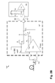
- connection interface of the data source is effected between the connection interface of the data source and the connection interface of the data sink, for example by means of a copper cable KK (with impedance Z 0 per differential pair of copper wires; cf. FIG. 3 ).
- the TMDS encoded signals are provided as output current signal from the data source by means of an output current driver (transmitter TM with current source SQ and changeover switch D, D′; cf. FIG. 3 ).
- the correct line termination in the receiver (receiver RC; cf. FIG. 3 ) is effected by the direct voltage coupled transmission channel KK between the data source and the data sink.
- the input signal voltage necessary for the input amplifier EV is generated with reference to the supply voltage AVCC.
- FIG. 3 shows the above-described with regard to the prior art in form of a conceptual schematic circuit diagram for a differential TMDS signal wherein it can be further taken from FIG. 3 that the receiver RC adopts the direct voltage supply of the output current driver of the transmitter TM.
- the connection interface of the data source provides a voltage supply in the order of about five volt for the data sink, wherein said voltage supply may be loaded with not more than about 55 milliampere.
- TMDS encoded signals of an HDMI data connection are to be able to support data transmission rates of several gigabits per second and per differential pair of wires AD, AD′ (cf. FIG. 3 ) of the copper cable KK. This involves that highest-quality and thus expensive copper cables are to be used in case of longer distances between data source and data sink.
- the object of the present invention is to provide a circuit arrangement and a method for inexpensively transmitting signals from at least one data source to at least one data sink, said signals being TMDS encoded at least in part, in particular at least in a time slot manner, and in particular being assigned to at least one DVI data connection and/or to at least one HDMI data connection.
- circuit arrangement for transmitting signals from at least one data source to at least one data sink, said signals being TMDS encoded at least in part, in particular at least in a time slot manner, and in particular being assigned to at least one DVI data connection and/or to at least one HDMI data connection, wherein said circuit arrangement comprises:
- the driver circuit comprises at least one voltage increasing circuit, in particular being implemented as voltage doubler and/or in particular operating as direct voltage converter, by means of which voltage increasing circuit electrical energy, in particular electrical power, can be taken and/or given from a
- the driver circuit comprises at least one second switching transistor, in particular being implemented as source follower,
- the driver circuit comprises
- transimpedance converter circuit comprises
- This object is achieved by a method for transmitting signals from at least one data source to at least one data sink, said signals being TMDS encoded at least in part, in particular at least in a time slot manner, and in particular being assigned to at least one DVI data connection and/or to at least one HDMI data connection,
- signals being TMDS encoded at least in part, in particular at least in a time slot manner can be transported by way of optical signal transmission from at least one data source to at least one data sink, in particular on the basis of at least one DVI data connection and/or of at least one HDMI data connection.
- the optical signal transmission via glass fiber or via plastic material fiber, such as via plastic fiber represents a price-efficient alternative to high-quality expensive copper cables (, with said optical signal transmission causing a conversion of the electrical signal into an optical signal by means of at least one electro-optical converter and vice versa by means of at least one opto-electrical converter).
- the supply of the at least one driver circuit or of the at least one transimpedance converter circuit is effected exclusively by means of the voltages and currents provided at the connection interfaces, in particular at the DVI transmission interfaces or at the HDMI transmission interfaces, of the data source and of the data sink.
- the present invention thus makes use of the fact that the current supply of the at least one driver circuit or of the at least one transimpedance converter circuit does not result from a (or even several) additional external current supply source(s) but can rather be provided by the connection interfaces of the data source or of the data sink.
- the circuit arrangement with the at least one driver circuit according to the present invention and with the at least one transimpedance converter circuit according to the present invention represents a possibility to optically transmit the TMDS signals provided by the connection interface of the data source, without requiring an additional external current supply therefor.
- TMDS encoded signals can comprise data rates in the region of several gigabits per second
- the optical transmission, as enabled by means of the present invention, of such TMDS encoded signals via optical fibers permits the buildup of inexpensive signal connections, which do not emit electromagnetic radiation and which can transport high data rates with low attenuation from the data source to the data sink.
- the advantages due to the presently optical transmission have an effect in particular for cable lengths of more than about three meters.
- the driver circuit acting as a direct current to direct current converter acting as a direct current to direct current converter (DC to DC converter)
- DC to DC converter direct current to direct current converter
- the direct current portion as provided from the TMDS transmitter, is converted in effect into a modulated signal current for controlling the light-emitting element, meaning a transfer of the energy (power), as provided by the TMDS transmitter, to the light-emitting element.
- the transferred power is approximately the product of the flowing direct current portion and of the voltage difference between the node voltage at the output of the TMDS transmitter and the voltage supply in the order of about five volt, said voltage supply being also available at the TMDS interface.
- the present invention further relates to a cable connection for transmitting signals from at least one data source to at least one data sink, said signals being TMDS encoded at least in part, in particular at least in a time slot manner, and in particular being assigned to at least one DVI data connection and/or to at least one HDMI data connection, comprising at least one circuit arrangement according to the above-mentioned type.
- the provision of at least one such active optical transmission cable is based on the fact that the circuit arrangement, i.e. the at least one driver circuit and/or the at least one transimpedance converter circuit can be implemented in a very compact way, namely without external current supply, such that the driver and/or the transimpedance converter can be integrated in a commercial, in particular conventional or regular, DVI connector and/or HDMI connector.
- the present invention finally relates to the use of at least one circuit arrangement according to the above-mentioned type and/or of a method according to the above-mentioned type for the signal connection, in particular in at least one cable connection, for example in at least one active optical transmission cable, between at least one HDTV data source, for example at least one Blu-ray player, and at least one HDTV data sink, for example at least one flat screen with very high resolution.
- FIG. 1B in a conceptual schematic view a second exemplary embodiment of the first part, namely of the driver part, being implemented according to the present invention, of a circuit arrangement, wherein said driver part is operated according to the method of the present invention;
- FIG. 2A in a conceptual schematic view a first exemplary embodiment of the second part, namely of the transimpedance converter part, being implemented according to the present invention, of a circuit arrangement, wherein said transimpedance converter part is operated according to the method of the present invention;
- FIG. 2B in a conceptual schematic view a second exemplary embodiment of the second part, namely of the transimpedance converter part, being implemented according to the present invention, of a circuit arrangement, wherein said transimpedance converter part is operated according to the method of the present invention;
- FIG. 3 in a conceptual schematic view an example of a prior art circuit arrangement.
- driver circuit S 1 illustrated by FIG. 1A or of the driver circuit S 1 ′ illustrated by FIG. 1B according to the present invention and by means of the transimpedance converter circuit S 2 illustrated by FIG. 2A or of the transimpedance converter circuit S 2 ′ illustrated by FIG. 2B according to the present invention, which together define the circuit arrangement 100 (cf. FIG. 1A , FIG. 2A ) or the circuit arrangement 100 ′ (cf. FIG. 1B , FIG.
- all signals used for the image data transmission of a DVI and/or HDMI connection are transmitted in this way via optical channels from the DVI/HDMI source to the DVI/HDMI sink.
- FIG. 1A or FIG. 1B show the principal setup of the driver S 1 or S 1 ′ for the link with the connection interface IQ of the data source.
- This connection interface IQ of the data source provides a voltage supply VDVI/HDMI in the order of about five volt, said voltage supply VDVI/HDMI being able to supply up to about 55 milliampere.
- This supply voltage VDVI/HDMI is fed to the driver S 1 or S 1 ′, which comprises
- the term light or light-emitting is understood not only as the range of electromagnetic radiation visible to the eye, extending in a wavelength range from about 380 nanometers to about 780 nanometers which corresponds to a frequency of about 789 terahertz down to about 385 terahertz; rather, the term light or light-emitting is understood as the entire electromagnetic wavelength or frequency spectrum, including the spectrum not visible to the eye, in particular the I[nfra]R[ed] range (wavelength range up to about 2,000 nanometers or frequency range down to about 150 terahertz), for example a wavelength of about 850 nanometers or a frequency of about 350 terahertz].
- the light-emitting element LD 1 couples the light LTMDS being supplied with the data signal into an optical fiber F 1 .
- a defined potential difference or voltage difference VLT 1 is generated by the voltage-limiting element LT 1 , with said potential difference or voltage difference VLT 1 representing the input voltage for the voltage increasing circuit DB 1 ;
- a defined termination voltage VTerm is generated by the voltage regulating element REG 1 , with said termination voltage VTerm representing the input voltage for the voltage increasing circuit DB 1 .
- the input terminal Vin of the voltage increasing circuit DB 1 is supplied
- the gate or the base of the switching transistor T 1 is connected with the output terminal of the amplifier DRV 1 .
- the drain or the collector of the switching transistor T 1 is assigned to the supply voltage VDVI/HDMI; in particular, the drain or the collector of the switching transistor T 1 lies essentially on supply voltage VDVI/HDMI.
- the source or the emitter of the switching transistor T 1 is connected with the input terminal of the light-emitting element LD 1 .
- the transistor T 2 operating as source follower that a minimum voltage is always applied to the light-emitting element LD 1 also during the phases in which the first transistor T 1 is off.
- a reduction of the switching-on delay of the light-emitting element LD 1 can be obtained whereby high signal frequencies are transmittable by the light-emitting element LD 1 .
- the gate or the base of the second switching transistor T 2 is assigned to the supply voltage VDVI/HDMI; in particular, the gate or the base of the second switching transistor T 2 can be chosen slightly differing from the supply voltage VDVI/HDMI in order to accomplish an optimization as to the most advantageous operating point of the light-emitting element LD 1 .
- the drain or the collector of the second switching transistor T 2 is assigned to the supply voltage VDVI/HDMI; in particular, the drain or the collector of the second switching transistor T 2 lies essentially on supply voltage VDVI/HDMI.
- the source or the emitter of the second switching transistor T 2 is connected with the source or the emitter of the switching transistor T 1 and with the input terminal of the light-emitting element LD 1 .
- the TMDS transmitter TM For the correct adjustment of the operating point of the output stage of the TMDS transmitter TM, the differential output of which is connected downstream of two transistors TS, TS' which are connected with respect to each other in a mirror-like way, the TMDS transmitter TM is supplied with
- the first terminating resistor RT 1 is connected between the input terminal of the voltage-limiting element LT 1 (cf. first exemplary embodiment of the driver S 1 according to FIG. 1A ) or of the voltage regulator REG 1 (cf. second exemplary embodiment of the driver S 1 ′ according to FIG. 1B ) and a first input terminal of the amplifier circuit DRV 1 ;
- the second terminating resistor RT 2 is connected between the input terminal of the voltage-limiting element LT 1 (cf. first exemplary embodiment of the driver S 1 according to FIG. 1A ) or of the voltage regulator REG 1 (cf. second exemplary embodiment of the driver S 1 ′ according to FIG. 1B ) and a second input terminal of the amplifier circuit DRV 1 .
- FIG. 2A or FIG. 2B show the basic setup of the transimpedance converter S 2 or S 2 ′ for the link with the connection interface IS of the data sink.
- This connection interface IS of the data sink has no explicit voltage supply which could supply the necessary energy to the transimpedance converter S 2 or S 2 ′.
- the TMDS receiver RC of the connection interface IS of the data sink effects that the TMDS transmitter TM is correctly terminated and that the necessary operating voltage is supplied to the output stage of the TMDS transmitter TM via the differential pair of wires AD, AD′ between data source and data sink; in particular, the transimpedance converter circuit S 2 or S 2 ′ is supplied by the direct voltage portion being applied to the differential pair of wires AD, AD′. This is used by the transimpedance converter circuit S 2 or S 2 ′ comprising an amplifier TIA 1 and resistors R 1 , R 2 , R 3 .
- the transimpedance converter circuit S 2 or S 2 ′ comprising an amplifier TIA 1 and resistors R 1 , R 2 , R 3 .
- the TMDS receiver RC of the connection interface IS of the data sink supplies an operating voltage AVCC in the order of about 3.3 volt, said operating voltage AVCC being able to supply up to about twelve milliampere per differential input and said supplying of the operating voltage AVCC being effected by internal ohmic terminating resistors RT, RT′ connected in parallel at the differential input of the TMDS receiver RC.
- the input signal voltage required for the input amplifier EV is generated at the termination RT, RT′ in the TMDS receiver RC referenced to this operating voltage AVCC.
- the transimpedance converter part S 2 or S 2 ′ Being connected to the differential input of the TMDS receiver RC, the transimpedance converter part S 2 or S 2 ′ generates for the TMDS receiver RC the VCM or common mode voltage required for the adjustment of the correct operating point, with said VCM or common mode voltage being generated from the correspondingly supplied operating voltage AVCC by the (terminating) resistors R 1 , R 2 provided for the purpose of at least partial termination of the differential connection line AD, AD′ (in this connection, the VCM or common mode voltage is a characteristic value of operational amplifiers or difference amplifiers, namely the mean value of the input voltages at the operational amplifier or difference amplifier).
- this voltage is smoothed by the capacitor C 5 .
- this voltage is provided to the amplifier TIA 1 as supply voltage for the reverse voltage VPD of a photo diode PD 1 assigned to the transimpedance converter S 2 .
- the supply current Isupply feeding the supply voltage Vsupply flows at least partially via the first (terminating) resistor R 1 or via the second (terminating) resistor R 2 from the differential pair of wires AD, AD′ to the amplifier TIA 1 .
- the current from the output stage is used as operating current or supply current Isupply of the amplifier TIA 1 .
- the voltage is conducted from this circuit node point via the series resistor R 3 to the two silicon diodes D 1 , D 2 .
- the correct operating voltage Vsupply of about 1.4 volt for the amplifier TIA 1 is generated at the node point R 1 , D 2 , C 4 by the voltage drop typical for a silicon diode D 1 , D 2 , with the differential input of the amplifier TIA 1 being assigned to the light-absorbing element PD 1 .
- This voltage is smoothed by means of the decoupling capacitor C 4 .
- the first switching transistor T 3 is assigned to the first output of the amplifier TIA 1 ; the second switching transistor T 4 is assigned to the second output of the amplifier TIA 1 , which provides the inversely to the first output of the amplifier TIA 1 phased signal of the differential output signal.
- the gate or the base of the first switching transistor T 3 is connected with the first output terminal of the amplifier TIA 1 ; the drain or the collector of the first switching transistor T 3 is assigned to the first (terminating) resistor R 1 ; the source or the emitter of the first switching transistor T 3 lies via the series resistor R 3 on operating voltage or supply voltage Vsupply for the amplifier TIA 1 .
- the gate or the base of the second switching transistor T 4 is connected with the second output terminal of the amplifier TIA 1 ; the drain or the collector of the second switching transistor T 4 is assigned to the second (terminating) resistor R 2 ; the source or the emitter of the second switching transistor T 4 is connected with the source or emitter of the first switching transistor T 3 and lies via the series resistor R 3 on operating voltage or supply voltage Vsupply for the amplifier TIA 1 .
- the gate or the base of the second switching transistor T 4 is connected with the second output terminal of the amplifier TIA 1 ; the drain or the collector of the second switching transistor T 4 is assigned to the second (terminating) resistor R 2 ; the source or the emitter of the second switching transistor T 4 is connected with the source or emitter of the first switching transistor T 3 and lies via the series resistor R 3 on operating voltage or supply voltage Vsupply for the amplifier TIA 1 .
- the supply current Isupply of the amplifier TIA 1 is alternately taken either from the first wire AD or from the second wire AD′ such that this supply current Isupply is essentially used for modulating the output voltage of the differential pair of wires AD, AD′ in dependence on the incoming optical signal.
- the supply current Isupply is at least partially the current flowing through the pair of switching transistors T 3 , T 4 , with said supply current Isupply feeding the supply voltage Vsupply of the amplifier TIA 1 .
- the current from the output stage is used as operating current or supply current Isupply of the amplifier TIA 1 .
- the electrical power required for operating the transimpedance converter circuit S 2 or S 2 ′ is taken from the power, which is the product of the direct current portion in the connection between the transimpedance converter circuit S 2 or S 2 ′ and the TMDS receiver RC and of the direct voltage portion at the TMDS receiver RC.
- the electrical power for operating the amplifier TIA 1 of the transimpedance converter circuit S 2 or S 2 ′ is taken from that electrical power, which is the product of the direct current portion in the connection between the transimpedance converter circuit S 2 or S 2 ′ and the TMDS receiver RC and of the potential difference or voltage difference between the node voltage at the output of the TMDS transmitter TM and the voltage supply also available at the TMDS interface in the order of about three volt.
Landscapes
- Engineering & Computer Science (AREA)
- Multimedia (AREA)
- Signal Processing (AREA)
- Physics & Mathematics (AREA)
- Electromagnetism (AREA)
- Theoretical Computer Science (AREA)
- General Physics & Mathematics (AREA)
- Computer Networks & Wireless Communication (AREA)
- Computer Hardware Design (AREA)
- Dc Digital Transmission (AREA)
- Optical Communication System (AREA)
- Two-Way Televisions, Distribution Of Moving Picture Or The Like (AREA)
- Electronic Switches (AREA)
- Logic Circuits (AREA)
- Optical Couplings Of Light Guides (AREA)
Applications Claiming Priority (7)
| Application Number | Priority Date | Filing Date | Title |
|---|---|---|---|
| DE102008042724 | 2008-10-09 | ||
| DE102008042724.1 | 2008-10-09 | ||
| DE102008042724 | 2008-10-09 | ||
| DE102009029683 | 2009-09-22 | ||
| DE102009029683.2 | 2009-09-22 | ||
| DE102009029683 | 2009-09-22 | ||
| PCT/EP2009/063131 WO2010040816A2 (de) | 2008-10-09 | 2009-10-09 | Schaltungsanordnung und verfahren zum übertragen von tmds-kodierten signalen |
Related Parent Applications (1)
| Application Number | Title | Priority Date | Filing Date |
|---|---|---|---|
| PCT/EP2009/063131 Continuation WO2010040816A2 (de) | 2008-10-09 | 2009-10-09 | Schaltungsanordnung und verfahren zum übertragen von tmds-kodierten signalen |
Publications (2)
| Publication Number | Publication Date |
|---|---|
| US20110268451A1 US20110268451A1 (en) | 2011-11-03 |
| US8824898B2 true US8824898B2 (en) | 2014-09-02 |
Family
ID=41818910
Family Applications (1)
| Application Number | Title | Priority Date | Filing Date |
|---|---|---|---|
| US13/083,282 Active 2030-07-27 US8824898B2 (en) | 2008-10-09 | 2011-04-08 | Circuit arrangement and method for transmitting TMDS encoded signals |
Country Status (4)
| Country | Link |
|---|---|
| US (1) | US8824898B2 (https=) |
| EP (1) | EP2359502B1 (https=) |
| JP (1) | JP5556817B2 (https=) |
| WO (1) | WO2010040816A2 (https=) |
Cited By (10)
| Publication number | Priority date | Publication date | Assignee | Title |
|---|---|---|---|---|
| US20150010311A1 (en) * | 2013-07-03 | 2015-01-08 | Cosemi Technologies, Inc. | Hybrid electrical-optical data communications cable with wireline capacitance compensation |
| US9397751B2 (en) | 2014-04-14 | 2016-07-19 | Cosemi Technologies, Inc. | Bidirectional data communications cable |
| US9641250B2 (en) | 2011-09-28 | 2017-05-02 | Cosemi Technologies, Inc. | System and method for communicating high and low speed data via optical signals and power via electrical signals |
| US20180190109A1 (en) * | 2016-12-30 | 2018-07-05 | Caavo Inc | Transmission of infrared signals over a high-definition multimedia interface cable |
| US10326245B1 (en) | 2018-03-29 | 2019-06-18 | Cosemi Technologies, Inc. | Light illuminating data communication cable |
| US10734768B2 (en) | 2018-05-16 | 2020-08-04 | Cosemi Technologies, Inc. | Data communication cable assembly including electromagnetic shielding features |
| US11057074B2 (en) | 2019-07-18 | 2021-07-06 | Cosemi Technologies, Inc. | Data and power communication cable with galvanic isolation protection |
| US11165500B2 (en) | 2020-02-21 | 2021-11-02 | Mobix Labs, Inc. | Cascadable data communication cable assembly |
| US11175463B2 (en) | 2020-02-21 | 2021-11-16 | Mobix Labs, Inc. | Extendable optical-based data communication cable assembly |
| US11177855B2 (en) | 2020-02-21 | 2021-11-16 | Mobix Labs, Inc. | Extendable wire-based data communication cable assembly |
Families Citing this family (18)
| Publication number | Priority date | Publication date | Assignee | Title |
|---|---|---|---|---|
| US8272023B2 (en) * | 2006-11-02 | 2012-09-18 | Redmere Technology Ltd. | Startup circuit and high speed cable using the same |
| US7996584B2 (en) * | 2006-11-02 | 2011-08-09 | Redmere Technology Ltd. | Programmable cable with deskew and performance analysis circuits |
| US8437973B2 (en) * | 2007-07-25 | 2013-05-07 | John Martin Horan | Boosted cable for carrying high speed channels and methods for calibrating the same |
| US7793022B2 (en) * | 2007-07-25 | 2010-09-07 | Redmere Technology Ltd. | Repeater for a bidirectional serial bus |
| US8280668B2 (en) * | 2007-07-25 | 2012-10-02 | Redmere Technology Ltd. | Self calibrating cable for high definition digital video interface |
| EP2665055A1 (en) | 2012-05-16 | 2013-11-20 | Nxp B.V. | Protection circuit for HDMI interface |
| US10033557B2 (en) | 2016-04-06 | 2018-07-24 | L-3 Communications Corporation | Isolated digital video interface receiver and method for isolating received digital video interface signals |
| US20220109906A1 (en) * | 2019-03-12 | 2022-04-07 | Wingcomm Co. Ltd. | Optical Data Interconnect System |
| US20220109500A1 (en) * | 2019-03-12 | 2022-04-07 | Wingcomm Co. Ltd. | Optical Data Interconnect System |
| US20220109510A1 (en) * | 2019-03-12 | 2022-04-07 | WINGCOMM Co, Ltd. | Optical Data Interconnect System |
| CN110661991A (zh) * | 2019-03-12 | 2020-01-07 | 飞昂创新科技南通有限公司 | 目标供电的光学数据互连系统 |
| CN110572625B (zh) * | 2019-03-12 | 2022-03-18 | 飞昂创新科技南通有限公司 | 光学数据互连系统 |
| CN110572602B (zh) * | 2019-03-12 | 2021-10-15 | 飞昂创新科技南通有限公司 | 用于光学数据互连系统的激活的电池触发 |
| WO2022130130A1 (en) | 2020-12-08 | 2022-06-23 | Silicon Line Gmbh | Circuit arrangement and method for transmitting tmds encoded signals |
| CN112865779A (zh) * | 2021-01-06 | 2021-05-28 | 季华实验室 | 信号转换电路及转换装置 |
| JP7375796B2 (ja) * | 2021-09-09 | 2023-11-08 | カシオ計算機株式会社 | 電子機器 |
| WO2023111874A1 (en) * | 2021-12-16 | 2023-06-22 | Wingcomm Co. Ltd. | Optical data interconnect system |
| WO2023111876A1 (en) * | 2021-12-16 | 2023-06-22 | Wingcomm Co. Ltd. | Optical data interconnect system |
Citations (52)
| Publication number | Priority date | Publication date | Assignee | Title |
|---|---|---|---|---|
| US5012384A (en) | 1990-02-20 | 1991-04-30 | Advanced Micro Device, Inc. | Load circuit for a differential driver |
| US5019769A (en) | 1990-09-14 | 1991-05-28 | Finisar Corporation | Semiconductor laser diode controller and laser diode biasing control method |
| US5672994A (en) | 1995-12-21 | 1997-09-30 | International Business Machines Corporation | Antifuse circuit using standard MOSFET devices |
| EP0798828A2 (en) | 1996-03-29 | 1997-10-01 | Fujitsu Limited | Light emitting element driving circuit and light emitting device having the same |
| US5834813A (en) | 1996-05-23 | 1998-11-10 | Micron Technology, Inc. | Field-effect transistor for one-time programmable nonvolatile memory element |
| US5949253A (en) | 1997-04-18 | 1999-09-07 | Adaptec, Inc. | Low voltage differential driver with multiple drive strengths |
| US20010043093A1 (en) | 2000-05-16 | 2001-11-22 | Shigeyuki Sakura | Led driving circuit and optical transmitting module |
| GB2365788A (en) | 2000-08-10 | 2002-02-27 | Mark Technology Corp Q | A signal transmitting/flashing adapter for a hand-held electronic game |
| US20020117724A1 (en) | 2001-02-19 | 2002-08-29 | Kawasaki Microelectronics Inc. | Semiconductor integrated circuit having anti-fuse, method of fabricating, and method of writing data in the same |
| US20030058725A1 (en) | 2001-09-25 | 2003-03-27 | Bell Debra M. | Antifuse programming current limiter |
| US20030094977A1 (en) | 2001-11-19 | 2003-05-22 | Broadcom Corporation | Voltage mode differential driver and method |
| US6650143B1 (en) | 2002-07-08 | 2003-11-18 | Kilopass Technologies, Inc. | Field programmable gate array based upon transistor gate oxide breakdown |
| US6667661B1 (en) | 2001-05-04 | 2003-12-23 | Euvis, Inc. | Laser diode driver with high power efficiency |
| US20040101007A1 (en) | 2002-11-27 | 2004-05-27 | Bozso Ferenc M. | High speed data channel including a CMOS VCSEL driver and a high performance photodetector and CMOS photoreceiver |
| US20040160996A1 (en) | 2003-01-02 | 2004-08-19 | Giorgi David M. | Apparatus and method for driving a pulsed laser diode |
| US20040195978A1 (en) | 2002-05-07 | 2004-10-07 | Sachito Horiuchi | Light emitting element drive device and electronic device light emitting element |
| US20040208011A1 (en) | 2002-05-07 | 2004-10-21 | Sachito Horiuchi | Light emitting element drive device and electronic device having light emitting element |
| US6812733B1 (en) | 2002-08-02 | 2004-11-02 | Pmc-Sierra, Inc. | High-efficiency mixed voltage/current mode output driver |
| US20050185428A1 (en) | 2004-02-19 | 2005-08-25 | Crawford Ian D. | Efficient fast pulsed laser or light-emitting diode driver |
| US6965722B1 (en) | 2004-10-29 | 2005-11-15 | Finisar Corporation | High efficiency active matching electro-optic transducer driver circuit operable with low supply voltages |
| US20050259703A1 (en) | 2004-05-19 | 2005-11-24 | Samsung Electronics Co., Ltd. And | Driving device and driving method for a light emitting device, and a display panel and display device having the driving device |
| US6975135B1 (en) | 2002-12-10 | 2005-12-13 | Altera Corporation | Universally programmable output buffer |
| US6990130B2 (en) | 2001-08-23 | 2006-01-24 | Sony Corporation | Semiconductor laser optical output control circuit and optical device |
| DE102004032456B3 (de) | 2004-06-30 | 2006-04-06 | Siemens Ag | Schaltungsanordnung zum Betreiben eines Leuchtzeichens |
| US20060077778A1 (en) * | 2004-09-29 | 2006-04-13 | Tatum Jimmy A | Consumer electronics with optical communication interface |
| US20060133435A1 (en) | 2001-03-05 | 2006-06-22 | Fuji Xerox Co., Ltd. | Apparatus for driving light emitting element and system for driving light emitting element |
| US20060147214A1 (en) | 2004-12-31 | 2006-07-06 | Ruiz Everardo D | Optically connecting computer components |
| US20060216034A1 (en) | 2005-03-23 | 2006-09-28 | Miller Rodney D | System and method of data transmission in tension members of a fiber optical system |
| US7133429B2 (en) | 2004-03-05 | 2006-11-07 | Finisar Corporation | Laser driver circuit with signal transition enhancement |
| US7154923B2 (en) | 2004-08-24 | 2006-12-26 | International Business Machines Corporation | Method and apparatus for providing a modulation current |
| US7173851B1 (en) | 2005-10-18 | 2007-02-06 | Kilopass Technology, Inc. | 3.5 transistor non-volatile memory cell using gate breakdown phenomena |
| FR2889643A1 (fr) | 2005-08-08 | 2007-02-09 | Valeo Systemes Thermiques | Ajustement de l'intensite lumineuse, notamment d'un tableau de commande pour vehicule automobile |
| WO2007027948A2 (en) | 2005-08-30 | 2007-03-08 | Finisar Corporation | Optical networks for consumer electronics |
| WO2007069104A1 (en) | 2005-12-12 | 2007-06-21 | Koninklijke Philips Electronics N.V. | System and method for opening web links in a browser application |
| US20070159434A1 (en) | 2006-01-12 | 2007-07-12 | Cheng-Chi Yen | Driving system of light emitting diode |
| US7272067B1 (en) | 2003-08-22 | 2007-09-18 | Altera Corporation | Electrically-programmable integrated circuit antifuses |
| US7280425B2 (en) | 2005-09-30 | 2007-10-09 | Intel Corporation | Dual gate oxide one time programmable (OTP) antifuse cell |
| US20070291807A1 (en) | 2006-06-14 | 2007-12-20 | Katsumi Uesaka | Optical transmitter with a shunt driving configuration and a load transistor operated in common gate mode |
| US20080007985A1 (en) | 2006-07-10 | 2008-01-10 | Wilcox William J | Antifuse circuit with well bias transistor |
| US20080012507A1 (en) | 2006-07-07 | 2008-01-17 | Mehmet Nalbant | High Current Fast Rise And Fall Time LED Driver |
| WO2008050779A1 (fr) | 2006-10-18 | 2008-05-02 | Koa Corporation | Circuit de commande de del |
| US20080154103A1 (en) | 2005-11-28 | 2008-06-26 | Lemay Charles R | Pulse Signal Drive Circuit |
| EP1956493A1 (en) | 2006-12-20 | 2008-08-13 | JDS Uniphase Corporation | Optical data link |
| US20080304527A1 (en) | 2007-06-07 | 2008-12-11 | Miaobin Gao | Controlling a bias current for an optical source |
| US7595661B2 (en) | 2004-12-17 | 2009-09-29 | Samsung Electronics Co., Ltd. | Low voltage differential signaling drivers including branches with series resistors |
| US7602739B2 (en) * | 2005-02-04 | 2009-10-13 | Avago Technologies Fiber Ip (Singapore) Pte. Ltd. | Communication arrangement and method for bidirectionally transmitting data between a first communication unit and a second communication unit |
| US20100109794A1 (en) | 2007-07-12 | 2010-05-06 | Martin Groepl | Circuit and method for driving at least one differential line |
| US20100172384A1 (en) | 2007-06-19 | 2010-07-08 | Martin Groepl | Circuit and method for controlling light-emitting components |
| US20100172385A1 (en) | 2007-06-19 | 2010-07-08 | Martin Groepl | Circuit and method for controlling light-emitting components |
| US20110080765A1 (en) | 2008-04-16 | 2011-04-07 | Silicon Line Gmbh | Programmable antifuse transistor and method for programming thereof |
| US20110121742A1 (en) | 2008-05-21 | 2011-05-26 | Silicon Line Gmbh | Circuit arrangement and method for controlling light emitting components |
| US8260148B2 (en) * | 2007-09-05 | 2012-09-04 | Stratos International, Inc. | Device for transmitting and receiving DVI video over a single fiber optic interconnect |
Family Cites Families (6)
| Publication number | Priority date | Publication date | Assignee | Title |
|---|---|---|---|---|
| JPS61163683A (ja) * | 1985-01-14 | 1986-07-24 | Nec Corp | レ−ザダイオ−ド駆動回路 |
| JPH07302943A (ja) * | 1994-03-09 | 1995-11-14 | Toshiba Corp | 駆動回路 |
| KR100402409B1 (ko) * | 2001-05-26 | 2003-10-30 | (주)오피트정보통신 | 원거리 전송이 가능한 디지털 비디오 신호 인터페이스 모듈 |
| JP3999184B2 (ja) * | 2003-09-30 | 2007-10-31 | 株式会社東芝 | 光信号受信装置及びdcオフセット調整回路 |
| JP4569195B2 (ja) * | 2003-11-14 | 2010-10-27 | 富士ゼロックス株式会社 | 信号伝送装置 |
| JP2007053675A (ja) * | 2005-08-19 | 2007-03-01 | Fuji Xerox Co Ltd | 光信号伝送装置 |
-
2009
- 2009-10-09 WO PCT/EP2009/063131 patent/WO2010040816A2/de not_active Ceased
- 2009-10-09 JP JP2011530492A patent/JP5556817B2/ja not_active Expired - Fee Related
- 2009-10-09 EP EP09752761.8A patent/EP2359502B1/de active Active
-
2011
- 2011-04-08 US US13/083,282 patent/US8824898B2/en active Active
Patent Citations (56)
| Publication number | Priority date | Publication date | Assignee | Title |
|---|---|---|---|---|
| US5012384A (en) | 1990-02-20 | 1991-04-30 | Advanced Micro Device, Inc. | Load circuit for a differential driver |
| US5019769A (en) | 1990-09-14 | 1991-05-28 | Finisar Corporation | Semiconductor laser diode controller and laser diode biasing control method |
| US5672994A (en) | 1995-12-21 | 1997-09-30 | International Business Machines Corporation | Antifuse circuit using standard MOSFET devices |
| EP0798828A2 (en) | 1996-03-29 | 1997-10-01 | Fujitsu Limited | Light emitting element driving circuit and light emitting device having the same |
| US6031855A (en) | 1996-03-29 | 2000-02-29 | Fujitsu Limited | Light emitting element driving circuit and light emitting device having the same |
| US5834813A (en) | 1996-05-23 | 1998-11-10 | Micron Technology, Inc. | Field-effect transistor for one-time programmable nonvolatile memory element |
| US5949253A (en) | 1997-04-18 | 1999-09-07 | Adaptec, Inc. | Low voltage differential driver with multiple drive strengths |
| US20010043093A1 (en) | 2000-05-16 | 2001-11-22 | Shigeyuki Sakura | Led driving circuit and optical transmitting module |
| GB2365788A (en) | 2000-08-10 | 2002-02-27 | Mark Technology Corp Q | A signal transmitting/flashing adapter for a hand-held electronic game |
| US20020117724A1 (en) | 2001-02-19 | 2002-08-29 | Kawasaki Microelectronics Inc. | Semiconductor integrated circuit having anti-fuse, method of fabricating, and method of writing data in the same |
| US20060133435A1 (en) | 2001-03-05 | 2006-06-22 | Fuji Xerox Co., Ltd. | Apparatus for driving light emitting element and system for driving light emitting element |
| US6667661B1 (en) | 2001-05-04 | 2003-12-23 | Euvis, Inc. | Laser diode driver with high power efficiency |
| US6990130B2 (en) | 2001-08-23 | 2006-01-24 | Sony Corporation | Semiconductor laser optical output control circuit and optical device |
| US20030058725A1 (en) | 2001-09-25 | 2003-03-27 | Bell Debra M. | Antifuse programming current limiter |
| US20030094977A1 (en) | 2001-11-19 | 2003-05-22 | Broadcom Corporation | Voltage mode differential driver and method |
| US20040195978A1 (en) | 2002-05-07 | 2004-10-07 | Sachito Horiuchi | Light emitting element drive device and electronic device light emitting element |
| US20040208011A1 (en) | 2002-05-07 | 2004-10-21 | Sachito Horiuchi | Light emitting element drive device and electronic device having light emitting element |
| US6650143B1 (en) | 2002-07-08 | 2003-11-18 | Kilopass Technologies, Inc. | Field programmable gate array based upon transistor gate oxide breakdown |
| US6812733B1 (en) | 2002-08-02 | 2004-11-02 | Pmc-Sierra, Inc. | High-efficiency mixed voltage/current mode output driver |
| US20040101007A1 (en) | 2002-11-27 | 2004-05-27 | Bozso Ferenc M. | High speed data channel including a CMOS VCSEL driver and a high performance photodetector and CMOS photoreceiver |
| US6975135B1 (en) | 2002-12-10 | 2005-12-13 | Altera Corporation | Universally programmable output buffer |
| US20040160996A1 (en) | 2003-01-02 | 2004-08-19 | Giorgi David M. | Apparatus and method for driving a pulsed laser diode |
| US7272067B1 (en) | 2003-08-22 | 2007-09-18 | Altera Corporation | Electrically-programmable integrated circuit antifuses |
| US20050185428A1 (en) | 2004-02-19 | 2005-08-25 | Crawford Ian D. | Efficient fast pulsed laser or light-emitting diode driver |
| US7133429B2 (en) | 2004-03-05 | 2006-11-07 | Finisar Corporation | Laser driver circuit with signal transition enhancement |
| US20050259703A1 (en) | 2004-05-19 | 2005-11-24 | Samsung Electronics Co., Ltd. And | Driving device and driving method for a light emitting device, and a display panel and display device having the driving device |
| DE102004032456B3 (de) | 2004-06-30 | 2006-04-06 | Siemens Ag | Schaltungsanordnung zum Betreiben eines Leuchtzeichens |
| US7154923B2 (en) | 2004-08-24 | 2006-12-26 | International Business Machines Corporation | Method and apparatus for providing a modulation current |
| US20060077778A1 (en) * | 2004-09-29 | 2006-04-13 | Tatum Jimmy A | Consumer electronics with optical communication interface |
| US6965722B1 (en) | 2004-10-29 | 2005-11-15 | Finisar Corporation | High efficiency active matching electro-optic transducer driver circuit operable with low supply voltages |
| US7595661B2 (en) | 2004-12-17 | 2009-09-29 | Samsung Electronics Co., Ltd. | Low voltage differential signaling drivers including branches with series resistors |
| US20060147214A1 (en) | 2004-12-31 | 2006-07-06 | Ruiz Everardo D | Optically connecting computer components |
| US7602739B2 (en) * | 2005-02-04 | 2009-10-13 | Avago Technologies Fiber Ip (Singapore) Pte. Ltd. | Communication arrangement and method for bidirectionally transmitting data between a first communication unit and a second communication unit |
| US20060216034A1 (en) | 2005-03-23 | 2006-09-28 | Miller Rodney D | System and method of data transmission in tension members of a fiber optical system |
| FR2889643A1 (fr) | 2005-08-08 | 2007-02-09 | Valeo Systemes Thermiques | Ajustement de l'intensite lumineuse, notamment d'un tableau de commande pour vehicule automobile |
| WO2007027948A2 (en) | 2005-08-30 | 2007-03-08 | Finisar Corporation | Optical networks for consumer electronics |
| US7280425B2 (en) | 2005-09-30 | 2007-10-09 | Intel Corporation | Dual gate oxide one time programmable (OTP) antifuse cell |
| EP1777708A1 (en) | 2005-10-18 | 2007-04-25 | Kilopass Technologies, Inc. | 3.5 Transistor non-volatile memory cell using gate breakdown phenomena |
| US7173851B1 (en) | 2005-10-18 | 2007-02-06 | Kilopass Technology, Inc. | 3.5 transistor non-volatile memory cell using gate breakdown phenomena |
| US20080154103A1 (en) | 2005-11-28 | 2008-06-26 | Lemay Charles R | Pulse Signal Drive Circuit |
| WO2007069104A1 (en) | 2005-12-12 | 2007-06-21 | Koninklijke Philips Electronics N.V. | System and method for opening web links in a browser application |
| US20070159434A1 (en) | 2006-01-12 | 2007-07-12 | Cheng-Chi Yen | Driving system of light emitting diode |
| US20070291807A1 (en) | 2006-06-14 | 2007-12-20 | Katsumi Uesaka | Optical transmitter with a shunt driving configuration and a load transistor operated in common gate mode |
| US20080012507A1 (en) | 2006-07-07 | 2008-01-17 | Mehmet Nalbant | High Current Fast Rise And Fall Time LED Driver |
| US20080007985A1 (en) | 2006-07-10 | 2008-01-10 | Wilcox William J | Antifuse circuit with well bias transistor |
| WO2008050779A1 (fr) | 2006-10-18 | 2008-05-02 | Koa Corporation | Circuit de commande de del |
| EP1956493A1 (en) | 2006-12-20 | 2008-08-13 | JDS Uniphase Corporation | Optical data link |
| US20080304527A1 (en) | 2007-06-07 | 2008-12-11 | Miaobin Gao | Controlling a bias current for an optical source |
| US20100172384A1 (en) | 2007-06-19 | 2010-07-08 | Martin Groepl | Circuit and method for controlling light-emitting components |
| US20100172385A1 (en) | 2007-06-19 | 2010-07-08 | Martin Groepl | Circuit and method for controlling light-emitting components |
| US20100109794A1 (en) | 2007-07-12 | 2010-05-06 | Martin Groepl | Circuit and method for driving at least one differential line |
| US8258813B2 (en) | 2007-07-12 | 2012-09-04 | Silicon Line Gmbh | Circuit and method for driving at least one differential line |
| US8260148B2 (en) * | 2007-09-05 | 2012-09-04 | Stratos International, Inc. | Device for transmitting and receiving DVI video over a single fiber optic interconnect |
| US20110080765A1 (en) | 2008-04-16 | 2011-04-07 | Silicon Line Gmbh | Programmable antifuse transistor and method for programming thereof |
| US8194431B2 (en) | 2008-04-16 | 2012-06-05 | Silicon Line Gmbh | Programmable antifuse transistor and method for programming thereof |
| US20110121742A1 (en) | 2008-05-21 | 2011-05-26 | Silicon Line Gmbh | Circuit arrangement and method for controlling light emitting components |
Non-Patent Citations (2)
| Title |
|---|
| HDMI (High-Definition Multimedia Interface Specification) Version 1.3a Hitachi, Ltd., et al., Nov. 10, 2006, (note p. 38 et seq.) (276 pages). |
| PCT International Search Report in application No. PCT/EP2009/063131, dated Mar. 29, 2010 (6 pages). |
Cited By (19)
| Publication number | Priority date | Publication date | Assignee | Title |
|---|---|---|---|---|
| US9641250B2 (en) | 2011-09-28 | 2017-05-02 | Cosemi Technologies, Inc. | System and method for communicating high and low speed data via optical signals and power via electrical signals |
| US10247891B2 (en) | 2011-09-28 | 2019-04-02 | Cosemi Technologies, Inc. | Method of manufacturing an optical communication mount |
| US9971115B2 (en) | 2011-09-28 | 2018-05-15 | Cosemi Technologies, Inc. | Data communications cable for communicating data and power via optical and electrical signals |
| US9979479B2 (en) | 2013-07-03 | 2018-05-22 | Cosemi Technologies, Inc. | Data communications cable with wireline capacitance compensation |
| US9397750B2 (en) * | 2013-07-03 | 2016-07-19 | Cosemi Technologies, Inc. | Hybrid electrical-optical data communications cable with wireline capacitance compensation |
| US9813153B2 (en) * | 2013-07-03 | 2017-11-07 | Cosemi Technologies, Inc. | Data communications cable with wireline capacitance compensation |
| US20150010311A1 (en) * | 2013-07-03 | 2015-01-08 | Cosemi Technologies, Inc. | Hybrid electrical-optical data communications cable with wireline capacitance compensation |
| US20160301472A1 (en) * | 2013-07-03 | 2016-10-13 | Cosemi Technologies, Inc. | Data communications cable with wireline capacitance compensation |
| US9813154B2 (en) | 2014-04-14 | 2017-11-07 | Cosemi Technologies, Inc. | Bidirectional data communications cable |
| US9397751B2 (en) | 2014-04-14 | 2016-07-19 | Cosemi Technologies, Inc. | Bidirectional data communications cable |
| US9979481B2 (en) | 2014-04-14 | 2018-05-22 | Cosemi Technologies, Inc. | Bidirectional data communications cable |
| US20180190109A1 (en) * | 2016-12-30 | 2018-07-05 | Caavo Inc | Transmission of infrared signals over a high-definition multimedia interface cable |
| US10282979B2 (en) * | 2016-12-30 | 2019-05-07 | Caavo Inc | Transmission of infrared signals over a high-definition multimedia interface cable |
| US10326245B1 (en) | 2018-03-29 | 2019-06-18 | Cosemi Technologies, Inc. | Light illuminating data communication cable |
| US10734768B2 (en) | 2018-05-16 | 2020-08-04 | Cosemi Technologies, Inc. | Data communication cable assembly including electromagnetic shielding features |
| US11057074B2 (en) | 2019-07-18 | 2021-07-06 | Cosemi Technologies, Inc. | Data and power communication cable with galvanic isolation protection |
| US11165500B2 (en) | 2020-02-21 | 2021-11-02 | Mobix Labs, Inc. | Cascadable data communication cable assembly |
| US11175463B2 (en) | 2020-02-21 | 2021-11-16 | Mobix Labs, Inc. | Extendable optical-based data communication cable assembly |
| US11177855B2 (en) | 2020-02-21 | 2021-11-16 | Mobix Labs, Inc. | Extendable wire-based data communication cable assembly |
Also Published As
| Publication number | Publication date |
|---|---|
| JP5556817B2 (ja) | 2014-07-23 |
| WO2010040816A3 (de) | 2010-06-17 |
| WO2010040816A2 (de) | 2010-04-15 |
| JP2012505582A (ja) | 2012-03-01 |
| EP2359502A2 (de) | 2011-08-24 |
| US20110268451A1 (en) | 2011-11-03 |
| EP2359502B1 (de) | 2017-04-05 |
Similar Documents
| Publication | Publication Date | Title |
|---|---|---|
| US8824898B2 (en) | Circuit arrangement and method for transmitting TMDS encoded signals | |
| US11233581B2 (en) | Battery triggering for activation of an optical data interconnect system | |
| US11233569B2 (en) | Optical data interconnect system | |
| US11233570B2 (en) | Sink powered optical data interconnect system | |
| TWI514789B (zh) | 用於建立及改良一通訊鏈路之方法及用於高速通訊之方法 | |
| US9882651B2 (en) | Methods, circuits and optical cable assemblies for optical transmission of high-speed data and low-speed data | |
| US7181100B2 (en) | Interconnect mechanism for connecting a laser driver to a laser | |
| US11757246B2 (en) | PSE device and powered device of optical power supply system, and optical power supply system | |
| US20220337318A1 (en) | Optical Data Interconnect System | |
| US11411660B2 (en) | Powered device, power sourcing equipment and power over fiber system | |
| US20050105574A1 (en) | Laser driver for optical communication network | |
| US20240356652A1 (en) | Light source multiplexing for modulated optical communication | |
| KR20160126119A (ko) | Ddc를 지원하는 광 hdmi 케이블 | |
| CN108418648A (zh) | 一种信号处理装置、方法以及一种智能网关设备 | |
| TWI771132B (zh) | 一種用於光通訊通道的源節點架構 | |
| CN223402530U (zh) | 一种hdmi的全光传输组件 | |
| CN111263219A (zh) | 无线供电通信系统 | |
| WO2022130130A1 (en) | Circuit arrangement and method for transmitting tmds encoded signals |
Legal Events
| Date | Code | Title | Description |
|---|---|---|---|
| AS | Assignment |
Owner name: SILICON LINE GMBH, GERMANY Free format text: ASSIGNMENT OF ASSIGNORS INTEREST;ASSIGNORS:GROEPL, MARTIN;HOELTKE, HOLGER;REEL/FRAME:026507/0437 Effective date: 20110627 |
|
| STCF | Information on status: patent grant |
Free format text: PATENTED CASE |
|
| MAFP | Maintenance fee payment |
Free format text: PAYMENT OF MAINTENANCE FEE, 4TH YR, SMALL ENTITY (ORIGINAL EVENT CODE: M2551) Year of fee payment: 4 |
|
| FEPP | Fee payment procedure |
Free format text: MAINTENANCE FEE REMINDER MAILED (ORIGINAL EVENT CODE: REM.); ENTITY STATUS OF PATENT OWNER: SMALL ENTITY |
|
| FEPP | Fee payment procedure |
Free format text: 7.5 YR SURCHARGE - LATE PMT W/IN 6 MO, SMALL ENTITY (ORIGINAL EVENT CODE: M2555); ENTITY STATUS OF PATENT OWNER: SMALL ENTITY |
|
| MAFP | Maintenance fee payment |
Free format text: PAYMENT OF MAINTENANCE FEE, 8TH YR, SMALL ENTITY (ORIGINAL EVENT CODE: M2552); ENTITY STATUS OF PATENT OWNER: SMALL ENTITY Year of fee payment: 8 |
|
| MAFP | Maintenance fee payment |
Free format text: PAYMENT OF MAINTENANCE FEE, 12TH YR, SMALL ENTITY (ORIGINAL EVENT CODE: M2553); ENTITY STATUS OF PATENT OWNER: SMALL ENTITY Year of fee payment: 12 |