US8809857B2 - Thin film transistor comprising oxide semiconductor - Google Patents
Thin film transistor comprising oxide semiconductor Download PDFInfo
- Publication number
- US8809857B2 US8809857B2 US14/028,617 US201314028617A US8809857B2 US 8809857 B2 US8809857 B2 US 8809857B2 US 201314028617 A US201314028617 A US 201314028617A US 8809857 B2 US8809857 B2 US 8809857B2
- Authority
- US
- United States
- Prior art keywords
- thin film
- film transistor
- channel layer
- gate
- insulating layer
- Prior art date
- Legal status (The legal status is an assumption and is not a legal conclusion. Google has not performed a legal analysis and makes no representation as to the accuracy of the status listed.)
- Expired - Fee Related
Links
- 239000010409 thin film Substances 0.000 title claims abstract description 56
- 239000004065 semiconductor Substances 0.000 title claims abstract description 46
- 150000004767 nitrides Chemical class 0.000 claims abstract description 25
- 229910052782 aluminium Inorganic materials 0.000 claims abstract description 22
- ZOXJGFHDIHLPTG-UHFFFAOYSA-N Boron Chemical compound [B] ZOXJGFHDIHLPTG-UHFFFAOYSA-N 0.000 claims abstract description 18
- XAGFODPZIPBFFR-UHFFFAOYSA-N aluminium Chemical compound [Al] XAGFODPZIPBFFR-UHFFFAOYSA-N 0.000 claims abstract description 18
- 229910052796 boron Inorganic materials 0.000 claims abstract description 18
- 239000000758 substrate Substances 0.000 claims description 26
- 239000000463 material Substances 0.000 claims description 20
- XOLBLPGZBRYERU-UHFFFAOYSA-N tin dioxide Chemical compound O=[Sn]=O XOLBLPGZBRYERU-UHFFFAOYSA-N 0.000 claims description 16
- VYPSYNLAJGMNEJ-UHFFFAOYSA-N Silicium dioxide Chemical compound O=[Si]=O VYPSYNLAJGMNEJ-UHFFFAOYSA-N 0.000 claims description 11
- 229910052814 silicon oxide Inorganic materials 0.000 claims description 11
- 229910004205 SiNX Inorganic materials 0.000 claims description 9
- 229910017107 AlOx Inorganic materials 0.000 claims description 8
- 229910007541 Zn O Inorganic materials 0.000 claims description 8
- 239000011810 insulating material Substances 0.000 claims description 8
- 229910052751 metal Inorganic materials 0.000 claims description 8
- 239000002184 metal Substances 0.000 claims description 8
- 229910020923 Sn-O Inorganic materials 0.000 claims description 6
- 229910007604 Zn—Sn—O Inorganic materials 0.000 claims description 5
- 238000004519 manufacturing process Methods 0.000 abstract description 5
- XLOMVQKBTHCTTD-UHFFFAOYSA-N Zinc monoxide Chemical compound [Zn]=O XLOMVQKBTHCTTD-UHFFFAOYSA-N 0.000 description 38
- 238000000034 method Methods 0.000 description 17
- 238000004544 sputter deposition Methods 0.000 description 14
- NBIIXXVUZAFLBC-UHFFFAOYSA-N Phosphoric acid Chemical compound OP(O)(O)=O NBIIXXVUZAFLBC-UHFFFAOYSA-N 0.000 description 12
- 238000000231 atomic layer deposition Methods 0.000 description 10
- PMHQVHHXPFUNSP-UHFFFAOYSA-M copper(1+);methylsulfanylmethane;bromide Chemical compound Br[Cu].CSC PMHQVHHXPFUNSP-UHFFFAOYSA-M 0.000 description 9
- 238000005229 chemical vapour deposition Methods 0.000 description 7
- PNEYBMLMFCGWSK-UHFFFAOYSA-N aluminium oxide Inorganic materials [O-2].[O-2].[O-2].[Al+3].[Al+3] PNEYBMLMFCGWSK-UHFFFAOYSA-N 0.000 description 6
- 229910000147 aluminium phosphate Inorganic materials 0.000 description 6
- 238000000151 deposition Methods 0.000 description 6
- 239000011701 zinc Substances 0.000 description 6
- 238000000137 annealing Methods 0.000 description 5
- 239000000203 mixture Substances 0.000 description 5
- 229920002120 photoresistant polymer Polymers 0.000 description 5
- GRYLNZFGIOXLOG-UHFFFAOYSA-N Nitric acid Chemical compound O[N+]([O-])=O GRYLNZFGIOXLOG-UHFFFAOYSA-N 0.000 description 4
- 229910021417 amorphous silicon Inorganic materials 0.000 description 4
- QVGXLLKOCUKJST-UHFFFAOYSA-N atomic oxygen Chemical compound [O] QVGXLLKOCUKJST-UHFFFAOYSA-N 0.000 description 4
- APFVFJFRJDLVQX-UHFFFAOYSA-N indium atom Chemical compound [In] APFVFJFRJDLVQX-UHFFFAOYSA-N 0.000 description 4
- PJXISJQVUVHSOJ-UHFFFAOYSA-N indium(III) oxide Inorganic materials [O-2].[O-2].[O-2].[In+3].[In+3] PJXISJQVUVHSOJ-UHFFFAOYSA-N 0.000 description 4
- 229910017604 nitric acid Inorganic materials 0.000 description 4
- 229910052760 oxygen Inorganic materials 0.000 description 4
- 239000001301 oxygen Substances 0.000 description 4
- 238000004549 pulsed laser deposition Methods 0.000 description 4
- GYHNNYVSQQEPJS-UHFFFAOYSA-N Gallium Chemical compound [Ga] GYHNNYVSQQEPJS-UHFFFAOYSA-N 0.000 description 3
- HCHKCACWOHOZIP-UHFFFAOYSA-N Zinc Chemical compound [Zn] HCHKCACWOHOZIP-UHFFFAOYSA-N 0.000 description 3
- 230000008021 deposition Effects 0.000 description 3
- 238000005530 etching Methods 0.000 description 3
- 229910052733 gallium Inorganic materials 0.000 description 3
- 229910052738 indium Inorganic materials 0.000 description 3
- 238000000623 plasma-assisted chemical vapour deposition Methods 0.000 description 3
- 229910021420 polycrystalline silicon Inorganic materials 0.000 description 3
- 239000002210 silicon-based material Substances 0.000 description 3
- 229910052725 zinc Inorganic materials 0.000 description 3
- 229920001621 AMOLED Polymers 0.000 description 2
- 229910018514 Al—O—N Inorganic materials 0.000 description 2
- IJGRMHOSHXDMSA-UHFFFAOYSA-N Atomic nitrogen Chemical compound N#N IJGRMHOSHXDMSA-UHFFFAOYSA-N 0.000 description 2
- 229910052581 Si3N4 Inorganic materials 0.000 description 2
- XUIMIQQOPSSXEZ-UHFFFAOYSA-N Silicon Chemical compound [Si] XUIMIQQOPSSXEZ-UHFFFAOYSA-N 0.000 description 2
- 230000008901 benefit Effects 0.000 description 2
- 229910052804 chromium Inorganic materials 0.000 description 2
- 150000001875 compounds Chemical class 0.000 description 2
- 229920001940 conductive polymer Polymers 0.000 description 2
- 238000001312 dry etching Methods 0.000 description 2
- 229910001195 gallium oxide Inorganic materials 0.000 description 2
- 239000011521 glass Substances 0.000 description 2
- 229910052737 gold Inorganic materials 0.000 description 2
- 238000007737 ion beam deposition Methods 0.000 description 2
- 238000000059 patterning Methods 0.000 description 2
- 239000000843 powder Substances 0.000 description 2
- SBIBMFFZSBJNJF-UHFFFAOYSA-N selenium;zinc Chemical compound [Se]=[Zn] SBIBMFFZSBJNJF-UHFFFAOYSA-N 0.000 description 2
- 229910052710 silicon Inorganic materials 0.000 description 2
- 239000010703 silicon Substances 0.000 description 2
- HQVNEWCFYHHQES-UHFFFAOYSA-N silicon nitride Chemical compound N12[Si]34N5[Si]62N3[Si]51N64 HQVNEWCFYHHQES-UHFFFAOYSA-N 0.000 description 2
- 229910052709 silver Inorganic materials 0.000 description 2
- 238000005245 sintering Methods 0.000 description 2
- 238000000992 sputter etching Methods 0.000 description 2
- 238000006467 substitution reaction Methods 0.000 description 2
- OFIYHXOOOISSDN-UHFFFAOYSA-N tellanylidenegallium Chemical compound [Te]=[Ga] OFIYHXOOOISSDN-UHFFFAOYSA-N 0.000 description 2
- 229910052719 titanium Inorganic materials 0.000 description 2
- 238000001039 wet etching Methods 0.000 description 2
- PIGFYZPCRLYGLF-UHFFFAOYSA-N Aluminum nitride Chemical compound [Al]#N PIGFYZPCRLYGLF-UHFFFAOYSA-N 0.000 description 1
- 229910052582 BN Inorganic materials 0.000 description 1
- PZNSFCLAULLKQX-UHFFFAOYSA-N Boron nitride Chemical compound N#B PZNSFCLAULLKQX-UHFFFAOYSA-N 0.000 description 1
- 229910007717 ZnSnO Inorganic materials 0.000 description 1
- 229910007611 Zn—In—O Inorganic materials 0.000 description 1
- 238000005280 amorphization Methods 0.000 description 1
- 239000000969 carrier Substances 0.000 description 1
- 238000002425 crystallisation Methods 0.000 description 1
- 230000008025 crystallization Effects 0.000 description 1
- AJNVQOSZGJRYEI-UHFFFAOYSA-N digallium;oxygen(2-) Chemical compound [O-2].[O-2].[O-2].[Ga+3].[Ga+3] AJNVQOSZGJRYEI-UHFFFAOYSA-N 0.000 description 1
- 230000000694 effects Effects 0.000 description 1
- 230000001747 exhibiting effect Effects 0.000 description 1
- 239000011888 foil Substances 0.000 description 1
- QZQVBEXLDFYHSR-UHFFFAOYSA-N gallium(III) oxide Inorganic materials O=[Ga]O[Ga]=O QZQVBEXLDFYHSR-UHFFFAOYSA-N 0.000 description 1
- 238000002513 implantation Methods 0.000 description 1
- 229910003437 indium oxide Inorganic materials 0.000 description 1
- 229910052746 lanthanum Inorganic materials 0.000 description 1
- 238000005224 laser annealing Methods 0.000 description 1
- 229910044991 metal oxide Inorganic materials 0.000 description 1
- 150000004706 metal oxides Chemical class 0.000 description 1
- 150000002739 metals Chemical class 0.000 description 1
- 238000001451 molecular beam epitaxy Methods 0.000 description 1
- 229910052759 nickel Inorganic materials 0.000 description 1
- 229910052757 nitrogen Inorganic materials 0.000 description 1
- 239000004033 plastic Substances 0.000 description 1
- 239000004984 smart glass Substances 0.000 description 1
- QHGNHLZPVBIIPX-UHFFFAOYSA-N tin(ii) oxide Chemical compound [Sn]=O QHGNHLZPVBIIPX-UHFFFAOYSA-N 0.000 description 1
- RNWHGQJWIACOKP-UHFFFAOYSA-N zinc;oxygen(2-) Chemical compound [O-2].[Zn+2] RNWHGQJWIACOKP-UHFFFAOYSA-N 0.000 description 1
Images


Classifications
-
- H—ELECTRICITY
- H01—ELECTRIC ELEMENTS
- H01L—SEMICONDUCTOR DEVICES NOT COVERED BY CLASS H10
- H01L29/00—Semiconductor devices adapted for rectifying, amplifying, oscillating or switching, or capacitors or resistors with at least one potential-jump barrier or surface barrier, e.g. PN junction depletion layer or carrier concentration layer; Details of semiconductor bodies or of electrodes thereof ; Multistep manufacturing processes therefor
- H01L29/66—Types of semiconductor device ; Multistep manufacturing processes therefor
- H01L29/66007—Multistep manufacturing processes
- H01L29/66075—Multistep manufacturing processes of devices having semiconductor bodies comprising group 14 or group 13/15 materials
- H01L29/66227—Multistep manufacturing processes of devices having semiconductor bodies comprising group 14 or group 13/15 materials the devices being controllable only by the electric current supplied or the electric potential applied, to an electrode which does not carry the current to be rectified, amplified or switched, e.g. three-terminal devices
- H01L29/66409—Unipolar field-effect transistors
- H01L29/66477—Unipolar field-effect transistors with an insulated gate, i.e. MISFET
- H01L29/66742—Thin film unipolar transistors
-
- H—ELECTRICITY
- H01—ELECTRIC ELEMENTS
- H01L—SEMICONDUCTOR DEVICES NOT COVERED BY CLASS H10
- H01L29/00—Semiconductor devices adapted for rectifying, amplifying, oscillating or switching, or capacitors or resistors with at least one potential-jump barrier or surface barrier, e.g. PN junction depletion layer or carrier concentration layer; Details of semiconductor bodies or of electrodes thereof ; Multistep manufacturing processes therefor
- H01L29/66—Types of semiconductor device ; Multistep manufacturing processes therefor
- H01L29/68—Types of semiconductor device ; Multistep manufacturing processes therefor controllable by only the electric current supplied, or only the electric potential applied, to an electrode which does not carry the current to be rectified, amplified or switched
- H01L29/76—Unipolar devices, e.g. field effect transistors
- H01L29/772—Field effect transistors
- H01L29/78—Field effect transistors with field effect produced by an insulated gate
- H01L29/786—Thin film transistors, i.e. transistors with a channel being at least partly a thin film
- H01L29/7869—Thin film transistors, i.e. transistors with a channel being at least partly a thin film having a semiconductor body comprising an oxide semiconductor material, e.g. zinc oxide, copper aluminium oxide, cadmium stannate
-
- H—ELECTRICITY
- H01—ELECTRIC ELEMENTS
- H01L—SEMICONDUCTOR DEVICES NOT COVERED BY CLASS H10
- H01L29/00—Semiconductor devices adapted for rectifying, amplifying, oscillating or switching, or capacitors or resistors with at least one potential-jump barrier or surface barrier, e.g. PN junction depletion layer or carrier concentration layer; Details of semiconductor bodies or of electrodes thereof ; Multistep manufacturing processes therefor
- H01L29/66—Types of semiconductor device ; Multistep manufacturing processes therefor
- H01L29/68—Types of semiconductor device ; Multistep manufacturing processes therefor controllable by only the electric current supplied, or only the electric potential applied, to an electrode which does not carry the current to be rectified, amplified or switched
- H01L29/76—Unipolar devices, e.g. field effect transistors
- H01L29/772—Field effect transistors
- H01L29/78—Field effect transistors with field effect produced by an insulated gate
- H01L29/786—Thin film transistors, i.e. transistors with a channel being at least partly a thin film
- H01L29/78606—Thin film transistors, i.e. transistors with a channel being at least partly a thin film with supplementary region or layer in the thin film or in the insulated bulk substrate supporting it for controlling or increasing the safety of the device
-
- H—ELECTRICITY
- H01—ELECTRIC ELEMENTS
- H01L—SEMICONDUCTOR DEVICES NOT COVERED BY CLASS H10
- H01L29/00—Semiconductor devices adapted for rectifying, amplifying, oscillating or switching, or capacitors or resistors with at least one potential-jump barrier or surface barrier, e.g. PN junction depletion layer or carrier concentration layer; Details of semiconductor bodies or of electrodes thereof ; Multistep manufacturing processes therefor
- H01L29/66—Types of semiconductor device ; Multistep manufacturing processes therefor
- H01L29/66007—Multistep manufacturing processes
- H01L29/66969—Multistep manufacturing processes of devices having semiconductor bodies not comprising group 14 or group 13/15 materials
-
- H—ELECTRICITY
- H01—ELECTRIC ELEMENTS
- H01L—SEMICONDUCTOR DEVICES NOT COVERED BY CLASS H10
- H01L29/00—Semiconductor devices adapted for rectifying, amplifying, oscillating or switching, or capacitors or resistors with at least one potential-jump barrier or surface barrier, e.g. PN junction depletion layer or carrier concentration layer; Details of semiconductor bodies or of electrodes thereof ; Multistep manufacturing processes therefor
- H01L29/66—Types of semiconductor device ; Multistep manufacturing processes therefor
- H01L29/68—Types of semiconductor device ; Multistep manufacturing processes therefor controllable by only the electric current supplied, or only the electric potential applied, to an electrode which does not carry the current to be rectified, amplified or switched
- H01L29/76—Unipolar devices, e.g. field effect transistors
- H01L29/772—Field effect transistors
- H01L29/78—Field effect transistors with field effect produced by an insulated gate
- H01L29/786—Thin film transistors, i.e. transistors with a channel being at least partly a thin film
- H01L29/78696—Thin film transistors, i.e. transistors with a channel being at least partly a thin film characterised by the structure of the channel, e.g. multichannel, transverse or longitudinal shape, length or width, doping structure, or the overlap or alignment between the channel and the gate, the source or the drain, or the contacting structure of the channel
Definitions
- the present invention relates to a thin film transistor and a method of fabricating the same, and more particularly, to an oxide thin film transistor in which a semiconductor thin film formed by combining an oxide semiconductor with a specific nitride is applied to a channel layer of a thin film transistor and a method of a fabricating the same.
- materials used to form a channel layer largely include silicon-based materials, ZnO-based materials, and non-ZnO-based materials. A detailed description of these materials will be provided below.
- Zn/O zinc to oxygen
- the characteristics of single crystallization are improved through a grain growth method and a low-temperature molecular beam epitaxy (MBE) process, and the characteristics of amorphization are improved using quaternary materials including indium, gallium, zinc, and oxygen.
- MBE low-temperature molecular beam epitaxy
- the quaternary materials including indium, gallium, zinc, and oxygen have been patented by Hosono, Japan, and thus use of them may require a license.
- Non-ZnO-based materials include In—Ga—Zn—O type amorphous semiconductor and individual oxide semiconductors such as In 2 O 3 and SnO 2 .
- the In—Ga—Zn—O type amorphous semiconductor is unlikely to be free from the original patent of Hosono.
- individual oxide semiconductors such as In 2 O 3 and SnO 2 have inferior characteristics to ZnO, they have not undergone sufficient research and there is room for improvement of their characteristics by composition adjustment and doping substitution.
- Non-ZnO-based materials include opaque semiconductors such as CdS, ZnS, ZnSe, etc., whose characteristics are applicable to active matrix organic light emitting diodes (AM OLED), but whose opacity is technically restrictive.
- thin film transistors using silicon-based materials, ZnO-based materials, and non-ZnO-based materials exhibit the following problems.
- a ZnO-based thin film transistor's characteristics are susceptible to changes in humidity, annealing processes, and manufacturing processes, and thus it has problems of reliability. Further, the transistor has a crystalline channel which may raise problems of device uniformity. Moreover, device deformation caused by current and light may be significant.
- indium and gallium are relatively scarce and therefore costly materials.
- amorphous silicon In a silicon-based thin film transistor, in particular, amorphous silicon, mobility is low, and with polycrystalline silicon, uniformity may be a problem in creation of a large panel. In particular, the amorphous silicon transistor is vulnerable to instability depending on current.
- an oxide thin film transistor may be vulnerable to instability depending on current due to the inside of a channel thin film or an interface with a gate insulating layer.
- a thin film transistor using ZnS, ZnSe, CdS, etc. is opaque and thus may not be applicable to transparent electronic devices.
- the present invention is directed to a thin film transistor capable of ensuring increased mobility and stability at a high temperature by applying a semiconductor thin film formed of an oxide semiconductor combined with a specific nitride to a channel layer.
- the present invention is also directed to a method of fabricating a thin film transistor capable of ensuring increased mobility and stability at a high temperature by optimizing a fabricating process including forming a semiconductor thin film formed of an oxide semiconductor combined with a specific nitride as a channel layer.
- An aspect of the present invention provides a thin film transistor comprising source and drain electrodes, a channel layer, a gate insulating layer and a gate electrode disposed on a substrate, the channel layer including an oxide semiconductor combined with a nitride containing boron or aluminum.
- the transistor may further include a channel protection layer formed of at least one insulating material selected from the group consisting of AlOx, SiNx and SiOx on the channel layer.
- the thin film transistor may have a top gate coplanar structure in which source and drain electrodes, a channel layer, a gate insulating layer and a gate electrode are sequentially stacked on a substrate, a top gate staggered structure in which a channel layer, source and drain electrodes, a gate insulating layer and a gate electrode are sequentially stacked on a substrate, a bottom gate coplanar structure in which a gate electrode, a gate insulating layer, source and drain electrodes and a channel layer are sequentially stacked on a substrate or a bottom gate staggered structure in which a gate electrode, a gate insulating layer, a channel layer and source and drain electrodes are sequentially stacked on a substrate.
- the oxide semiconductor used for the channel layer may be formed of at least one selected from the group consisting of ZnO, In—Zn—O, Zn—Sn—O, In—Ga—ZnO, Zn—In—Sn—O, In—Ga—O and SnO 2 , the nitride containing boron or aluminum may include BN or AlN, and the nitride containing boron or aluminum may be included such that the boron or aluminum may exist within a range of 0.01 to 50 at % on the basis of the total atomic weight of metal atoms of an oxide semiconductor constituting the semiconductor thin film.
- the gate insulating layer may be formed of at least one insulating material selected from the group consisting of AlOx, SiNx and SiOx.
- Another aspect of the present invention provides a method of fabricating a thin film transistor, comprising: forming source and drain electrodes, a channel layer, a gate insulating layer and a gate electrode on a substrate, the channel layer being formed of a semiconductor thin film formed of an oxide semiconductor combined with a nitride containing boron or aluminum; and patterning the channel layer.
- the method may further include forming a channel protection layer on the channel layer using an insulating material, the channel protection layer being patterned together with the channel layer.
- the oxide semiconductor may be formed of at least one material selected from the group consisting of ZnO, In—Zn—O, Zn—Sn—O, In—Ga—ZnO, Zn—In—Sn—O, In—Ga—O and SnO 2 , and the nitride containing boron or aluminum may be included such that the boron or aluminum may exist within a range of 0.01 to 50 at % on the basis of the total atomic weight of metal atoms of an oxide semiconductor constituting the semiconductor thin film.
- the channel layer may be formed by depositing the oxide semiconductor combined with the nitride to a thickness of 5 to 100 nm by sputtering, pulsed laser deposition (PLD) or ion-beam deposition at a temperature of room temperature to 300° C., and by performing post-annealing at a temperature below 600° C.
- PLD pulsed laser deposition
- ion-beam deposition ion-beam deposition
- the channel protection layer may be formed to a thickness of 1 nm to 20 nm using at least one material selected from the group consisting of AlOx, SiNx and SiOx by chemical vapor deposition (CVD), atomic layer deposition (ALD) or sputtering method.
- CVD chemical vapor deposition
- ALD atomic layer deposition
- sputtering method a material selected from the group consisting of AlOx, SiNx and SiOx by chemical vapor deposition (CVD), atomic layer deposition (ALD) or sputtering method.
- the patterning may be performed using photoresist, etching may be performed by dry or wet etching or ion milling or by fabricating a lift-off pattern using the photoresist, and the photoresist may be applied at a temperature lower that 150° C.
- the gate insulating layer may be formed using at least one insulating material selected from the group consisting of AlOx, SiNx and SiOx by ALD.
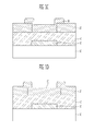
- FIGS. 1A to 1D are cross-sectional views of a structure of a thin film transistor according to one exemplary embodiment of the present invention.
- FIGS. 2A to 2D are cross-sectional views of a structure of a thin film transistor according to another exemplary embodiment of the present invention.
- FIG. 3 is a transfer plot of a thin film transistor fabricated from Embodiment 1.
- FIG. 4 is a transfer plot of a thin film transistor fabricated from Embodiment 2.
- a thin film transistor according to the present invention may constitute a top gate thin film transistor having a coplanar structure in which source and drain electrodes 20 , a channel layer 30 , a gate insulating layer 40 and a gate electrode 50 are sequentially stacked on a substrate 10 or an inverted staggered structure in which a channel layer 30 , source and drain electrodes 20 , a gate insulating layer 40 and a gate electrode 50 are sequentially stacked on a substrate 10 .
- it may constitute a bottom gate thin film transistor having a coplanar structure in which a gate electrode 50 , a gate insulating layer 40 , source and drain electrodes 20 and a channel layer 30 are sequentially stacked on a substrate 10 or a staggered structure in which a gate electrode 50 , a gate insulating layer 40 , a channel layer 30 , and source and drain electrodes 20 are sequentially stacked on a substrate 10 .
- a thin film transistor according to another exemplary embodiment of the present invention further includes a channel protection layer A on a channel layer 30 .
- a thin film transistor according to the present invention includes source and drain electrodes 20 , a channel layer 30 , a channel protection layer A, a gate insulating layer 40 and a gate electrode 50 on a substrate 10 .
- the substrate 10 may be one generally used in this field of art, and for example, may be one selected from glass, metal foil, plastic and silicon.
- the source and drain electrodes 20 formed on the substrate 10 While a transparent oxide such as ITO, IZO, ZnO:Al(Ga), etc., a metal such as Al, Cr, Au, Ag, Ti, etc., or a conductive polymer may be used as the source and drain electrodes 20 formed on the substrate 10 , the present invention is not limited thereto. Moreover, the source and drain electrodes 20 may form a double-layer structure of the metal and the oxide. The source and drain electrodes 20 are deposited to a normal thickness using a process such as sputtering, atomic layer deposition (ALD) and chemical vapor deposition (CVD), and then the results are patterned.
- ALD atomic layer deposition
- CVD chemical vapor deposition
- the channel layer 30 formed in a channel region on the substrate 10 and the source and drain electrodes 20 is deposited to a thickness of 5 nm to 100 nm using an oxide semiconductor combined with a nitride containing boron or aluminum.
- Deposition may be performed using a normal deposition method used in this field, and more preferably, sputtering, pulsed laser deposition (PLD) or ion-beam deposition may be employed. While the sputtering deposition is performed, an oxide target combined with a nitride may be used, and a nitride target and an oxide target may be separately mounted to simultaneously perform sputtering. Nitride powder and oxide power may be sufficiently mixed and the results may be sintered at a temperature of 900° C. to 1500° C. to fabricate a target. In this case, a sintering temperature and atmosphere may vary depending on types of powder and an amount thereof, and the sintering may be performed under an oxygen, nitrogen or vacuum atmosphere.
- the channel layer 30 may be deposited at a temperature of 450° C. or lower, and more preferably, may be deposited at room temperature to 300° C.
- a post-annealing process may be performed at a temperature of 600° C. or lower, and more preferably, may be performed at a temperature of 300° C. to 600° C.
- the oxide semiconductor may include a zinc oxide-, tin oxide-, indium oxide-, or gallium oxide-based semiconductor, and more preferably, it may include ZnO, In—Zn—O(In2O 3 —ZnO), Zn—Sn—O(ZnO—SnO 2 ), Zn—In—Sn—O(ZnO—In 2 O 3 —SnO 2 ), In—Ga—Zn—O(In 2 O 3 —Ga 2 O 3 —ZnO), In—Ga—O(In 2 O 3 Ga 2 O 3 ) or SnO 2 .
- BN or AlN may be used as the nitride containing boron or aluminum combined with the oxide semiconductor, and boron nitride or aluminum nitride may be included such that boron or aluminum exists within a range of 0.01 to 50 at % on the basis of the total atomic weight of metal atoms of a metal oxide constituting the semiconductor thin film.
- the addition of the BN or AlN may result in improved stability at a high temperature in addition to increased mobility.
- the channel protection layer A may be selectively formed on the channel layer 30 .
- the channel protection layer A may be formed to protect the channel layer from being etched, may be formed to a thickness of 1 nm to 20 nm, and may be formed of an insulating material such as AlOx, SiNx or SiOx
- the channel protection layer A may be formed using CVD, ALD, or sputtering.
- the channel layer 30 or the channel layer 30 and the channel protection layer A may be patterned using ion milling, dry etching, wet etching or lift-off.
- the lift-off may be performed by forming a lift-off pattern using photoresist, and here, the photoresist is vulnerable to a deposition temperature, and thus may be applied at a temperature below 150° C.
- the gate insulating layer 40 partially forming at least an interface with the channel layer 30 may be formed by depositing alumina, silicon nitride or silicon oxide at a temperature of 450° C. or lower.
- the alumina may be deposited using ALD, plasma enhanced chemical vapor deposition (PECVD) or metalorganic chemical vapor deposition (MOCVD) at a temperature of 100° C. to 250° C.
- PECVD plasma enhanced chemical vapor deposition
- MOCVD metalorganic chemical vapor deposition
- the silicon nitride (SiNx) or silicon oxide (SiOx) may be deposited using PECVD at a temperature of 100° C. to 300° C., and in the case of a high temperature process, a temperature below 500° C. may be applied.
- a post-annealing process may be performed at a temperature of 200° C. to 300° C. for stability.
- a transparent oxide such as ITO, IZO or ZnO:Al(Ga)
- various kinds of metals exhibiting a low resistance such as Ti, Ag, Au, Al, Cr, Al/Cr/Al or Ni, or a conductive polymer
- the gate electrode 50 is deposited to a normal thickness in this field using sputtering, ALD or CVD, and then is patterned.
- a channel protection layer was formed to a thickness of 10 nm on the channel layer using alumina. Subsequently, the channel layer and the channel protection layer were wet etched using a diluted HF solution to be patterned. Then, alumina was used to be deposited on the patterned channel layer and channel protection layer by ALD at a temperature of 150° C., so that a gate insulating layer was formed to a thickness of 190 nm. Afterwards, the gate insulating layer was etched using a phosphoric acid solution heated up to 120° C. to be patterned.
- a gate electrode was deposited to a thickness of 150 nm on the gate insulating layer using ITO by sputtering, and the results were etched using a mixture solution of phosphoric acid and nitric acid at a temperature of 50° C. to be patterned, so that a thin film transistor was fabricated. Characteristics of the obtained transistor were evaluated, and the evaluated results are shown in FIG. 3 . As confirmed from FIG. 3 , SS was equal to 0.33, and mobility was 22.18 cm 2 /sV.
- a channel protection layer was formed to a thickness of 10 nm on the channel layer using alumina. Subsequently, the channel layer and the channel protection layer were wet etched using a diluted HF solution to be patterned. Then, alumina was used to be deposited on the patterned channel layer and channel protection layer by ALD at a temperature of 150° C., so that a gate insulating layer was formed to a thickness of 190 nm. Afterwards, the gate insulating layer was etched using a phosphoric acid solution heated up to 120° C. to be patterned.
- a gate electrode was deposited to a thickness of 150 nm on the gate insulating layer using ITO by sputtering, and the results were etched using a mixture solution of phosphoric acid and nitric acid at a temperature of 50° C. to be patterned, so that a thin film transistor was fabricated. Characteristics of the obtained transistor were evaluated, and the evaluated results are shown in FIG. 4 . As confirmed from FIG. 4 , SS was equal to 0.40, and mobility was 17.96 cm 2 /sV.
- the thin film transistor in which an oxide semiconductor combined with AlN is used as the channel layer exhibits enhanced electrical characteristics.
- the thin film transistor in which an oxide semiconductor combined with AlN is used as the channel layer has numerous applications, and may be used for designing various transparent circuits in addition to displays.
- it may be used for a medical transparent display panel, an electronic circuit, UN PD, a transparent LED, a bi-directional transparent monitor panel, as a driving device of an LCD or OLED panel, a transparent RFID tag, a smart window that functions as both a transparent glass window and a display, a head-up display (HUD) of a car or airplane, a head mounted display (HMD) a general-purpose transparent display or a flexible, transparent display, etc.
- HUD head-up display
- HMD head mounted display
- the present invention exhibits the following effects.
- a semiconductor thin film formed of an oxide semiconductor combined with a nitride exhibits increased mobility and improved electrical characteristics compared to a conventional semiconductor thin film, and increases usability of a device.
- a semiconductor thin film formed of an oxide semiconductor combined with a nitride according to the present invention exhibits stability at a high temperature, and thus can have high resistance against a temperature that may be caused during a process.
Abstract
Description
Claims (11)
Priority Applications (1)
| Application Number | Priority Date | Filing Date | Title |
|---|---|---|---|
| US14/028,617 US8809857B2 (en) | 2009-12-11 | 2013-09-17 | Thin film transistor comprising oxide semiconductor |
Applications Claiming Priority (4)
| Application Number | Priority Date | Filing Date | Title |
|---|---|---|---|
| KR1020090122990A KR20110066370A (en) | 2009-12-11 | 2009-12-11 | Oxide thin film transistor and method for manufacturing the same |
| KR10-2009-0122990 | 2009-12-11 | ||
| US12/887,282 US8563356B2 (en) | 2009-12-11 | 2010-09-21 | Thin film transistor and method of fabricating the same |
| US14/028,617 US8809857B2 (en) | 2009-12-11 | 2013-09-17 | Thin film transistor comprising oxide semiconductor |
Related Parent Applications (1)
| Application Number | Title | Priority Date | Filing Date |
|---|---|---|---|
| US12/887,282 Division US8563356B2 (en) | 2009-12-11 | 2010-09-21 | Thin film transistor and method of fabricating the same |
Publications (2)
| Publication Number | Publication Date |
|---|---|
| US20140008650A1 US20140008650A1 (en) | 2014-01-09 |
| US8809857B2 true US8809857B2 (en) | 2014-08-19 |
Family
ID=44141909
Family Applications (2)
| Application Number | Title | Priority Date | Filing Date |
|---|---|---|---|
| US12/887,282 Expired - Fee Related US8563356B2 (en) | 2009-12-11 | 2010-09-21 | Thin film transistor and method of fabricating the same |
| US14/028,617 Expired - Fee Related US8809857B2 (en) | 2009-12-11 | 2013-09-17 | Thin film transistor comprising oxide semiconductor |
Family Applications Before (1)
| Application Number | Title | Priority Date | Filing Date |
|---|---|---|---|
| US12/887,282 Expired - Fee Related US8563356B2 (en) | 2009-12-11 | 2010-09-21 | Thin film transistor and method of fabricating the same |
Country Status (3)
| Country | Link |
|---|---|
| US (2) | US8563356B2 (en) |
| JP (1) | JP5439287B2 (en) |
| KR (1) | KR20110066370A (en) |
Cited By (5)
| Publication number | Priority date | Publication date | Assignee | Title |
|---|---|---|---|---|
| US20150177311A1 (en) * | 2013-12-19 | 2015-06-25 | Intermolecular, Inc. | Methods and Systems for Evaluating IGZO with Respect to NBIS |
| US9391209B2 (en) | 2010-02-05 | 2016-07-12 | Semiconductor Energy Laboratory Co., Ltd. | Semiconductor device |
| US9905702B2 (en) | 2011-09-29 | 2018-02-27 | Semiconductor Energy Laboratory Co., Ltd. | Semiconductor device and method for manufacturing the same |
| US9997514B2 (en) | 2011-06-29 | 2018-06-12 | Semiconductor Energy Laboratory Co., Ltd. | Driver circuit, method of manufacturing the driver circuit, and display device including the driver circuit |
| US11271115B2 (en) | 2011-10-19 | 2022-03-08 | Semiconductor Energy Laboratory Co., Ltd. | Semiconductor device |
Families Citing this family (25)
| Publication number | Priority date | Publication date | Assignee | Title |
|---|---|---|---|---|
| CN101719493B (en) * | 2008-10-08 | 2014-05-14 | 株式会社半导体能源研究所 | Display device |
| KR20110066370A (en) * | 2009-12-11 | 2011-06-17 | 한국전자통신연구원 | Oxide thin film transistor and method for manufacturing the same |
| CN105590964B (en) * | 2010-02-05 | 2019-01-04 | 株式会社半导体能源研究所 | Semiconductor device |
| TWI476931B (en) * | 2010-10-21 | 2015-03-11 | Au Optronics Corp | Thin film transistor and pixel structure having the thin film transistor |
| US9219159B2 (en) * | 2011-03-25 | 2015-12-22 | Semiconductor Energy Laboratory Co., Ltd. | Method for forming oxide semiconductor film and method for manufacturing semiconductor device |
| TWI545652B (en) * | 2011-03-25 | 2016-08-11 | 半導體能源研究所股份有限公司 | Semiconductor device and manufacturing method thereof |
| TW201312757A (en) * | 2011-09-14 | 2013-03-16 | Hon Hai Prec Ind Co Ltd | Thin film transistor and method for manufacturing the same |
| US9018629B2 (en) * | 2011-10-13 | 2015-04-28 | Semiconductor Energy Laboratory Co., Ltd. | Semiconductor device and method for manufacturing semiconductor device |
| KR101283936B1 (en) * | 2011-12-09 | 2013-07-16 | 강릉원주대학교산학협력단 | Oxide semiconductor transistor and manufacturing method thereof |
| JP5910294B2 (en) * | 2012-05-10 | 2016-04-27 | 富士通株式会社 | Electronic device and manufacturing method of laminated structure |
| KR101346612B1 (en) * | 2012-05-21 | 2014-01-03 | 성균관대학교산학협력단 | Thin film transistor and producing method of the same |
| KR102004398B1 (en) | 2012-07-24 | 2019-07-29 | 삼성디스플레이 주식회사 | Display device and method of manufacturing the same |
| KR101927409B1 (en) | 2012-08-07 | 2018-12-10 | 삼성전자주식회사 | High electron mobility transistor |
| JP6229658B2 (en) * | 2012-09-21 | 2017-11-15 | 凸版印刷株式会社 | THIN FILM TRANSISTOR, MANUFACTURING METHOD THEREOF, AND IMAGE DISPLAY DEVICE |
| WO2014065985A1 (en) * | 2012-10-22 | 2014-05-01 | Applied Materials, Inc. | High mobility compound semiconductor material using multiple anions |
| JP6121149B2 (en) * | 2012-11-28 | 2017-04-26 | 富士フイルム株式会社 | Oxide semiconductor element, manufacturing method of oxide semiconductor element, display device, and image sensor |
| CN103915507A (en) * | 2012-12-31 | 2014-07-09 | 瀚宇彩晶股份有限公司 | Oxide thin film transistor structure and method for producing same |
| CN104409361A (en) * | 2014-12-16 | 2015-03-11 | 京东方科技集团股份有限公司 | Thin-film transistor, preparation method of thin-film transistor, array substrate and display device |
| CN106030821B (en) * | 2015-02-12 | 2019-11-12 | 深圳市柔宇科技有限公司 | Top-gate thin-film transistors, array substrate and its manufacturing method and TFT device |
| US9853210B2 (en) * | 2015-11-17 | 2017-12-26 | International Business Machines Corporation | Reduced process degradation of spin torque magnetoresistive random access memory |
| KR101876011B1 (en) * | 2016-01-29 | 2018-07-06 | 연세대학교 산학협력단 | Oxide thin film transistor and method of manufacturing the same |
| KR101914835B1 (en) * | 2016-11-18 | 2018-11-02 | 아주대학교산학협력단 | Metal oxide heterojunction structure, method of manufacturing the metal oxide heterojunction structure, and thin film transistor having the metal oxide heterojunction structure |
| KR102437514B1 (en) * | 2017-11-09 | 2022-08-26 | 엘지디스플레이 주식회사 | Thin film trnasistor having protecting layer for blocking hydrogen, method for manufacturing the same and display device comprising the same |
| KR102014132B1 (en) * | 2017-11-28 | 2019-08-26 | 광운대학교 산학협력단 | Fabrication method of solution-processed high quality Al2O3/BN dielectric films for high performance IGZO TFTs, and IGZO TFTs thereof |
| CN110233156A (en) * | 2019-07-05 | 2019-09-13 | 深圳市华星光电半导体显示技术有限公司 | The production method and thin film transistor base plate of thin film transistor base plate |
Citations (14)
| Publication number | Priority date | Publication date | Assignee | Title |
|---|---|---|---|---|
| JPH06291318A (en) | 1993-02-02 | 1994-10-18 | Fujitsu Ltd | Thin film transistor matrix device and manufacture thereof |
| US5712494A (en) | 1995-03-22 | 1998-01-27 | Kabushiki Kaisha Toshiba | Thin film field effect transistor having an extension portion acting as a light shield and back gate |
| JP2000228516A (en) | 1999-02-08 | 2000-08-15 | Tdk Corp | Semiconductor laminated thin film, electronic device and diode |
| JP2001322814A (en) | 2000-05-12 | 2001-11-20 | Kenkichiro Kobayashi | P-type oxide semiconductor and its manufacturing method |
| US20050017244A1 (en) | 2003-07-25 | 2005-01-27 | Randy Hoffman | Semiconductor device |
| KR20060132659A (en) | 2004-01-23 | 2006-12-21 | 휴렛-팩커드 디벨롭먼트 컴퍼니, 엘 피 | Transistor including a deposited channel region having a doped portion |
| JP2007073705A (en) | 2005-09-06 | 2007-03-22 | Canon Inc | Oxide-semiconductor channel film transistor and its method of manufacturing same |
| US7304331B2 (en) | 2004-07-14 | 2007-12-04 | Kabushiki Kaisha Toshiba | Nitride semiconductor device such as transverse power FET for high frequency signal amplification or power control |
| KR20080076608A (en) | 2007-02-16 | 2008-08-20 | 삼성전자주식회사 | Thin film transistor and method for forming the same |
| JP2009043920A (en) | 2007-08-08 | 2009-02-26 | Rohm Co Ltd | P-TYPE MgZnO-BASED THIN FILM AND SEMICONDUCTOR LIGHT-EMITTING ELEMENT |
| US20090166616A1 (en) | 2007-12-26 | 2009-07-02 | Hitachi, Ltd. | Oxide semiconductor device and surface treatment method of oxide semiconductor |
| JP2009272427A (en) | 2008-05-07 | 2009-11-19 | Canon Inc | Thin-film transistor and method of manufacturing the same |
| US20100155716A1 (en) | 2008-12-18 | 2010-06-24 | Electronics And Telecommunications Research Institute | Thin film transistor using boron-doped oxide semiconductor thin film and method of fabricating the same |
| JP2011124532A (en) | 2009-12-11 | 2011-06-23 | Korea Electronics Telecommun | Thin film transistor and method of fabricating the same |
-
2009
- 2009-12-11 KR KR1020090122990A patent/KR20110066370A/en active Search and Examination
-
2010
- 2010-06-16 JP JP2010137175A patent/JP5439287B2/en not_active Expired - Fee Related
- 2010-09-21 US US12/887,282 patent/US8563356B2/en not_active Expired - Fee Related
-
2013
- 2013-09-17 US US14/028,617 patent/US8809857B2/en not_active Expired - Fee Related
Patent Citations (17)
| Publication number | Priority date | Publication date | Assignee | Title |
|---|---|---|---|---|
| JPH06291318A (en) | 1993-02-02 | 1994-10-18 | Fujitsu Ltd | Thin film transistor matrix device and manufacture thereof |
| US5712494A (en) | 1995-03-22 | 1998-01-27 | Kabushiki Kaisha Toshiba | Thin film field effect transistor having an extension portion acting as a light shield and back gate |
| JP2000228516A (en) | 1999-02-08 | 2000-08-15 | Tdk Corp | Semiconductor laminated thin film, electronic device and diode |
| JP2001322814A (en) | 2000-05-12 | 2001-11-20 | Kenkichiro Kobayashi | P-type oxide semiconductor and its manufacturing method |
| US7564055B2 (en) | 2003-07-25 | 2009-07-21 | Hewlett-Packard Development Company, L.P. | Transistor including a deposited channel region having a doped portion |
| US20050017244A1 (en) | 2003-07-25 | 2005-01-27 | Randy Hoffman | Semiconductor device |
| KR20060132659A (en) | 2004-01-23 | 2006-12-21 | 휴렛-팩커드 디벨롭먼트 컴퍼니, 엘 피 | Transistor including a deposited channel region having a doped portion |
| US7304331B2 (en) | 2004-07-14 | 2007-12-04 | Kabushiki Kaisha Toshiba | Nitride semiconductor device such as transverse power FET for high frequency signal amplification or power control |
| JP2007073705A (en) | 2005-09-06 | 2007-03-22 | Canon Inc | Oxide-semiconductor channel film transistor and its method of manufacturing same |
| KR20080076608A (en) | 2007-02-16 | 2008-08-20 | 삼성전자주식회사 | Thin film transistor and method for forming the same |
| US7910920B2 (en) | 2007-02-16 | 2011-03-22 | Samsung Electronics Co., Ltd. | Thin film transistor and method of forming the same |
| JP2009043920A (en) | 2007-08-08 | 2009-02-26 | Rohm Co Ltd | P-TYPE MgZnO-BASED THIN FILM AND SEMICONDUCTOR LIGHT-EMITTING ELEMENT |
| US20090166616A1 (en) | 2007-12-26 | 2009-07-02 | Hitachi, Ltd. | Oxide semiconductor device and surface treatment method of oxide semiconductor |
| JP2009272427A (en) | 2008-05-07 | 2009-11-19 | Canon Inc | Thin-film transistor and method of manufacturing the same |
| US20110042670A1 (en) | 2008-05-07 | 2011-02-24 | Canon Kabushiki Kaisha | Thin film transistor and method of manufacturing the same |
| US20100155716A1 (en) | 2008-12-18 | 2010-06-24 | Electronics And Telecommunications Research Institute | Thin film transistor using boron-doped oxide semiconductor thin film and method of fabricating the same |
| JP2011124532A (en) | 2009-12-11 | 2011-06-23 | Korea Electronics Telecommun | Thin film transistor and method of fabricating the same |
Non-Patent Citations (2)
| Title |
|---|
| H.Q. Chiang et al., "High mobility transparent thin-film transistor with amorphous zinc tin oxide channle layer", Applied Physics Letters 86, 013503-1 to 013503-3(2005). |
| M.G. McDowell et al., "Combinatorial study of zinc tin oxide thin-film transistors", Applied Physics letters 92, 013502-1 to 013502-3 (2008). |
Cited By (6)
| Publication number | Priority date | Publication date | Assignee | Title |
|---|---|---|---|---|
| US9391209B2 (en) | 2010-02-05 | 2016-07-12 | Semiconductor Energy Laboratory Co., Ltd. | Semiconductor device |
| US9997514B2 (en) | 2011-06-29 | 2018-06-12 | Semiconductor Energy Laboratory Co., Ltd. | Driver circuit, method of manufacturing the driver circuit, and display device including the driver circuit |
| US9905702B2 (en) | 2011-09-29 | 2018-02-27 | Semiconductor Energy Laboratory Co., Ltd. | Semiconductor device and method for manufacturing the same |
| US11271115B2 (en) | 2011-10-19 | 2022-03-08 | Semiconductor Energy Laboratory Co., Ltd. | Semiconductor device |
| US11817505B2 (en) | 2011-10-19 | 2023-11-14 | Semiconductor Energy Laboratory Co., Ltd. | Semiconductor device |
| US20150177311A1 (en) * | 2013-12-19 | 2015-06-25 | Intermolecular, Inc. | Methods and Systems for Evaluating IGZO with Respect to NBIS |
Also Published As
| Publication number | Publication date |
|---|---|
| KR20110066370A (en) | 2011-06-17 |
| US8563356B2 (en) | 2013-10-22 |
| US20140008650A1 (en) | 2014-01-09 |
| US20110140097A1 (en) | 2011-06-16 |
| JP5439287B2 (en) | 2014-03-12 |
| JP2011124532A (en) | 2011-06-23 |
Similar Documents
| Publication | Publication Date | Title |
|---|---|---|
| US8809857B2 (en) | Thin film transistor comprising oxide semiconductor | |
| US8071434B2 (en) | Method of fabricating a thin film transistor using boron-doped oxide semiconductor thin film | |
| EP2115770B1 (en) | ELECTRONIC SEMICONDUCTOR DEVICE BASED ON COPPER NICKEL AND GALLIUM-TIN-ZINC-COPPER-TITANIUM p AND n-TYPE OXIDES, THEIR APPLICATIONS AND CORRESPONDING MANUFACTURE PROCESS | |
| JP5467728B2 (en) | Thin film field effect transistor and method of manufacturing the same | |
| US7906780B2 (en) | Field effect transistor | |
| US20100019239A1 (en) | Method of fabricating zto thin film, thin film transistor employing the same, and method of fabricating thin film transistor | |
| JP5371467B2 (en) | FIELD EFFECT TRANSISTOR AND METHOD FOR MANUFACTURING FIELD EFFECT TRANSISTOR | |
| KR101238823B1 (en) | The thin film transistor and the manufacuring method thereof | |
| KR101980196B1 (en) | Transistor, method of manufacturing the same and electronic device including transistor | |
| KR101344483B1 (en) | Thin Film Transistor | |
| US20130264565A1 (en) | Semiconductor thin film, thin film transistor and production method therefor | |
| KR20190045659A (en) | Thin film trnasistor comprising 2d semiconductor and display device comprising the same | |
| KR20150016789A (en) | Thin film transistor and method for fabricating the same | |
| KR101975929B1 (en) | Transistor having oxynitride channel layer and method of manufacturing the same | |
| JP2010050165A (en) | Semiconductor device, method of manufacturing the same, transistor substrate, light emitting device, and display device | |
| US20100006837A1 (en) | Composition for oxide semiconductor thin film, field effect transistor using the composition and method of fabricating the transistor | |
| KR20140144388A (en) | Thin film transistor array panel | |
| KR101849268B1 (en) | Highly stable thin film transistor under bias and illumination stress and fabrication method therof | |
| KR20110080118A (en) | Thin film transistor having etch stop multi-layers and method of manufacturing the same | |
| KR102550633B1 (en) | Thin film transistor substrate and manufacturing method thereof | |
| KR20100010888A (en) | Method for preparing zto thin film, thin film transistor using the same and method for preparing thin film transistor | |
| JP2012186383A (en) | Manufacturing method of thin-film transistor | |
| CN114175271A (en) | Thin film transistor, semiconductor substrate and X-ray flat panel detector | |
| AU2007346358B2 (en) | Electronic semiconductor device based on copper nickel and gallium-tin-zinc-copper-titanium p and n-type oxides, their applications and corresponding manufacture process | |
| KR20150018917A (en) | Thin film transistor having metal oxynitride channel layer and method of manufacturing the same and display including the same |
Legal Events
| Date | Code | Title | Description |
|---|---|---|---|
| AS | Assignment |
Owner name: ELECTRONICS AND TELECOMMUNICATIONS RESEARCH INSTIT Free format text: ASSIGNMENT OF ASSIGNORS INTEREST;ASSIGNORS:CHEONG, WOO SEOK;CHUNG, SUNG MOOK;BAK, JUN YONG;REEL/FRAME:031218/0889 Effective date: 20130903 |
|
| FEPP | Fee payment procedure |
Free format text: PAYOR NUMBER ASSIGNED (ORIGINAL EVENT CODE: ASPN); ENTITY STATUS OF PATENT OWNER: SMALL ENTITY |
|
| FEPP | Fee payment procedure |
Free format text: MAINTENANCE FEE REMINDER MAILED (ORIGINAL EVENT CODE: REM.) |
|
| LAPS | Lapse for failure to pay maintenance fees |
Free format text: PATENT EXPIRED FOR FAILURE TO PAY MAINTENANCE FEES (ORIGINAL EVENT CODE: EXP.); ENTITY STATUS OF PATENT OWNER: SMALL ENTITY |
|
| STCH | Information on status: patent discontinuation |
Free format text: PATENT EXPIRED DUE TO NONPAYMENT OF MAINTENANCE FEES UNDER 37 CFR 1.362 |
|
| FP | Lapsed due to failure to pay maintenance fee |
Effective date: 20180819 |