US8804065B2 - Flexible liquid crystal display and flexible fluid display - Google Patents
Flexible liquid crystal display and flexible fluid display Download PDFInfo
- Publication number
- US8804065B2 US8804065B2 US13/346,400 US201213346400A US8804065B2 US 8804065 B2 US8804065 B2 US 8804065B2 US 201213346400 A US201213346400 A US 201213346400A US 8804065 B2 US8804065 B2 US 8804065B2
- Authority
- US
- United States
- Prior art keywords
- module
- flexible
- display
- liquid crystal
- supporting structures
- Prior art date
- Legal status (The legal status is an assumption and is not a legal conclusion. Google has not performed a legal analysis and makes no representation as to the accuracy of the status listed.)
- Active, expires
Links
Images


Classifications
-
- G—PHYSICS
- G02—OPTICS
- G02B—OPTICAL ELEMENTS, SYSTEMS OR APPARATUS
- G02B26/00—Optical devices or arrangements for the control of light using movable or deformable optical elements
- G02B26/004—Optical devices or arrangements for the control of light using movable or deformable optical elements based on a displacement or a deformation of a fluid
- G02B26/005—Optical devices or arrangements for the control of light using movable or deformable optical elements based on a displacement or a deformation of a fluid based on electrowetting
-
- G—PHYSICS
- G02—OPTICS
- G02F—OPTICAL DEVICES OR ARRANGEMENTS FOR THE CONTROL OF LIGHT BY MODIFICATION OF THE OPTICAL PROPERTIES OF THE MEDIA OF THE ELEMENTS INVOLVED THEREIN; NON-LINEAR OPTICS; FREQUENCY-CHANGING OF LIGHT; OPTICAL LOGIC ELEMENTS; OPTICAL ANALOGUE/DIGITAL CONVERTERS
- G02F1/00—Devices or arrangements for the control of the intensity, colour, phase, polarisation or direction of light arriving from an independent light source, e.g. switching, gating or modulating; Non-linear optics
- G02F1/01—Devices or arrangements for the control of the intensity, colour, phase, polarisation or direction of light arriving from an independent light source, e.g. switching, gating or modulating; Non-linear optics for the control of the intensity, phase, polarisation or colour
- G02F1/13—Devices or arrangements for the control of the intensity, colour, phase, polarisation or direction of light arriving from an independent light source, e.g. switching, gating or modulating; Non-linear optics for the control of the intensity, phase, polarisation or colour based on liquid crystals, e.g. single liquid crystal display cells
- G02F1/133—Constructional arrangements; Operation of liquid crystal cells; Circuit arrangements
- G02F1/1333—Constructional arrangements; Manufacturing methods
- G02F1/133305—Flexible substrates, e.g. plastics, organic film
-
- G—PHYSICS
- G02—OPTICS
- G02F—OPTICAL DEVICES OR ARRANGEMENTS FOR THE CONTROL OF LIGHT BY MODIFICATION OF THE OPTICAL PROPERTIES OF THE MEDIA OF THE ELEMENTS INVOLVED THEREIN; NON-LINEAR OPTICS; FREQUENCY-CHANGING OF LIGHT; OPTICAL LOGIC ELEMENTS; OPTICAL ANALOGUE/DIGITAL CONVERTERS
- G02F1/00—Devices or arrangements for the control of the intensity, colour, phase, polarisation or direction of light arriving from an independent light source, e.g. switching, gating or modulating; Non-linear optics
- G02F1/01—Devices or arrangements for the control of the intensity, colour, phase, polarisation or direction of light arriving from an independent light source, e.g. switching, gating or modulating; Non-linear optics for the control of the intensity, phase, polarisation or colour
- G02F1/13—Devices or arrangements for the control of the intensity, colour, phase, polarisation or direction of light arriving from an independent light source, e.g. switching, gating or modulating; Non-linear optics for the control of the intensity, phase, polarisation or colour based on liquid crystals, e.g. single liquid crystal display cells
- G02F1/133—Constructional arrangements; Operation of liquid crystal cells; Circuit arrangements
- G02F1/1333—Constructional arrangements; Manufacturing methods
- G02F1/133377—Cells with plural compartments or having plurality of liquid crystal microcells partitioned by walls, e.g. one microcell per pixel
-
- G—PHYSICS
- G02—OPTICS
- G02F—OPTICAL DEVICES OR ARRANGEMENTS FOR THE CONTROL OF LIGHT BY MODIFICATION OF THE OPTICAL PROPERTIES OF THE MEDIA OF THE ELEMENTS INVOLVED THEREIN; NON-LINEAR OPTICS; FREQUENCY-CHANGING OF LIGHT; OPTICAL LOGIC ELEMENTS; OPTICAL ANALOGUE/DIGITAL CONVERTERS
- G02F1/00—Devices or arrangements for the control of the intensity, colour, phase, polarisation or direction of light arriving from an independent light source, e.g. switching, gating or modulating; Non-linear optics
- G02F1/01—Devices or arrangements for the control of the intensity, colour, phase, polarisation or direction of light arriving from an independent light source, e.g. switching, gating or modulating; Non-linear optics for the control of the intensity, phase, polarisation or colour
- G02F1/13—Devices or arrangements for the control of the intensity, colour, phase, polarisation or direction of light arriving from an independent light source, e.g. switching, gating or modulating; Non-linear optics for the control of the intensity, phase, polarisation or colour based on liquid crystals, e.g. single liquid crystal display cells
- G02F1/133—Constructional arrangements; Operation of liquid crystal cells; Circuit arrangements
- G02F1/1333—Constructional arrangements; Manufacturing methods
- G02F1/1339—Gaskets; Spacers; Sealing of cells
- G02F1/13394—Gaskets; Spacers; Sealing of cells spacers regularly patterned on the cell subtrate, e.g. walls, pillars
-
- G—PHYSICS
- G02—OPTICS
- G02F—OPTICAL DEVICES OR ARRANGEMENTS FOR THE CONTROL OF LIGHT BY MODIFICATION OF THE OPTICAL PROPERTIES OF THE MEDIA OF THE ELEMENTS INVOLVED THEREIN; NON-LINEAR OPTICS; FREQUENCY-CHANGING OF LIGHT; OPTICAL LOGIC ELEMENTS; OPTICAL ANALOGUE/DIGITAL CONVERTERS
- G02F1/00—Devices or arrangements for the control of the intensity, colour, phase, polarisation or direction of light arriving from an independent light source, e.g. switching, gating or modulating; Non-linear optics
- G02F1/01—Devices or arrangements for the control of the intensity, colour, phase, polarisation or direction of light arriving from an independent light source, e.g. switching, gating or modulating; Non-linear optics for the control of the intensity, phase, polarisation or colour
- G02F1/13—Devices or arrangements for the control of the intensity, colour, phase, polarisation or direction of light arriving from an independent light source, e.g. switching, gating or modulating; Non-linear optics for the control of the intensity, phase, polarisation or colour based on liquid crystals, e.g. single liquid crystal display cells
- G02F1/133—Constructional arrangements; Operation of liquid crystal cells; Circuit arrangements
- G02F1/1333—Constructional arrangements; Manufacturing methods
- G02F1/1339—Gaskets; Spacers; Sealing of cells
- G02F1/13396—Spacers having different sizes
Definitions
- the invention relates in general to a flexible liquid crystal display and a flexible fluid display, and more particularly to a flexible liquid crystal display and a flexible fluid display both having flexible and non-flexible areas.
- the display has the property of flexibility, the user can bend the display according to the needs.
- the display has a property similar to that of paper.
- the flexible display has the advantages of easy storage and portability, and has become one of the focuses in the research and development of the display technology.
- the spacers located at the bending positions may be deformed or broken.
- the invention is directed to a flexible liquid crystal display and a flexible fluid display, in which a space between the first module and the second module is divided into flexible area and non-flexible areas through a number of supporting structures.
- a flexible liquid crystal display including a first module, a second module, at least two supporting structures and a liquid crystal layer.
- the second module is disposed correspondingly to the first module.
- the supporting structures are separately disposed between the first module and the second module and used for abutting the first module and the second module, so that a space between the first module and the second module is divided into a flexible area and two non-flexible areas.
- the flexible area is located between two non-flexible areas.
- the liquid crystal layer is disposed in the flexible area and the two non-flexible areas.
- a flexible fluid display including a first module, a second module, at least two supporting structure and a fluid
- the first module includes an electrode layer and a hydrophobic material layer stacked in order.
- the second module is disposed correspondingly to the first module.
- the supporting structures are separately disposed between the first module and the second module and used for abutting the first module and the second module, so that a space between the first module and the second module is divided into a flexible area and two non-flexible areas.
- the flexible area is located between two non-flexible areas.
- a fluid is disposed in the flexible area and the two non-flexible areas.
- the electrode layer modifies the hydrophobic property of the hydrophobic material layer according to whether a voltage is received so as to make the fluid enter a different distribution state.
- FIG. 1A shows a top view of a first module of a flexible display and the structure thereof according to the first embodiment of the invention
- FIG. 1B shows a cross-sectional view of the flexible display of FIG. 1A ;
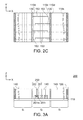
- FIG. 2A-FIG . 2 C respectively show the top views of other flexible displays according to the first embodiment of the invention.
- FIG. 3A shows a cross-sectional view of a flexible display according to the second embodiment of the invention.
- FIG. 3B shows a cross-sectional view of another flexible display according to the second embodiment of the invention.
- FIG. 4A and FIG. 4B respectively shows the cross-sectional views of a flexible fluid display in different states according to an embodiment of the invention.
- FIG. 5A and FIG. 5B respectively show the cross-sectional views of another flexible fluid display in different states according to an embodiment of the invention.
- FIG. 1A shows a top view of a first module of a flexible display and the structure thereof according to a first embodiment of the invention.
- FIG. 1B shows a cross-sectional view of the flexible display of FIG. 1A .
- the flexible display 100 includes a first module 110 , a second module 120 , at least two supporting structures 130 and a display medium 140 . To clearly illustrate the interior structure and disposition of the flexible display 100 , the second module 120 and the display medium 140 are not illustrated in FIG. 1A .
- the second module 120 is disposed correspondingly to the first module 110 .
- the supporting structures 130 are separately disposed between the first module 110 and the second module 120 and used for abutting the first module 110 and the second module 120 , so that a space between the first module 110 and the second module 120 is divided into a flexible area (fa) and two non-flexible areas (fn).
- the flexible area fa is located between two non-flexible areas fn.
- the display medium 140 is disposed in the flexible area fa and the two non-flexible areas fn. That is, the display medium 140 is filled in three independent closed areas formed by a flexible area fa and two non-flexible areas fn.
- the display medium 140 in the flexible area fa which is exerted by an external force would be blocked by the supporting structures 130 and would not be able to flow to the two non-flexible areas fn.
- the display medium 140 in the flexible area fa still remains in the flexible area fa
- the display medium 140 in the non-flexible areas fn still remains in the non-flexible areas fn, so that the flexible display 100 possesses stable display quality.
- the flexible display 100 further includes a number of sub-supporting structures 150 disposed in the flexible area fa and used for abutting the first module 110 and the second module 120 .
- the supporting structures 130 and the sub-supporting structures 150 can be formed on the first module 110 or the second module 120 by way of printing, transferring, lithography or spraying.
- the supporting structures 130 and the sub-supporting structures 150 can further be adhered to the first module 110 and the second module 120 , so that the structure of the flexible area fa is more stable and the display quality of the flexible display 100 can be more stably maintained.
- each supporting structure 130 and that of each sub-supporting structure 150 are substantially equal to the gap between the first module 110 and the second module 120 .
- the sub-supporting structures 150 also provide supporting function in the flexible area fa.
- the first module 110 includes a number of data lines 110 d and a number of scan lines 110 s .
- the data lines 110 d and the scan lines 110 s are interlaced with each other to form a number of pixel areas.
- the positions of two supporting structures 130 correspond to that of two of the data lines 110 d and extend along two of the data lines 110 d .
- the position of each sub-supporting structures 150 is disposed correspondingly to that of any of the data lines 110 d or any of the scan lines 110 s .
- a supporting structure 130 , a number of sub-supporting structures 150 and another supporting structure 130 are sequentially disposed correspondingly to the positions of adjacent data lines 110 d , and the supporting structures 130 and the sub-supporting structures 150 all extend along the Y-axis direction.
- none of the supporting structures 130 and the sub-supporting structures 150 is disposed in the pixel areas lest the supporting structures 130 and the sub-supporting structures 150 might affect the aperture ratio of the flexible display 100 when providing support.
- the supporting structures 130 and the sub-supporting structures 150 could be disposed in the pixel areas.
- each sub-supporting structure 150 could be disposed without corresponding to the adjacent data line 110 d as illustrated in FIG. 2A-FIG . 2 C.
- FIG. 2A-FIG . 2 C top views of other flexible displays according to a first embodiment of the invention are respectively shown.
- the sub-supporting structures 151 of FIG. 2A extend along the X-axis direction and correspond to a number of scan lines 110 s .
- a number of sub-supporting structures 152 of FIG. 2B also extend along the Y-axis direction and correspond to a number of data lines 110 d .
- Two ends of the adjacent sub-supporting structures 152 of FIG. 2B are not aligned with each other for enhancing the effect of blocking the display medium around the edges of the flexible display.
- the possibility of free-flow display medium is greatly decreased.
- a number of sub-supporting structures 153 of FIG. 2C also extend along the X-axis direction and correspond to a number of scan lines 110 s .
- Two ends of the adjacent sub-supporting structures 153 of FIG. 2C are not aligned with each other for enhancing the effect of blocking the display medium at the location near the supporting structures 130 .
- the possibility of free-flow display medium is greatly decreased.
- the cross-section of the sub-supporting structure is a rectangle; however, could be other shapes such as a trapezoid or others.
- the sub-supporting structures disposed on the XY plane are depicted as the shape of strips, as indicated in FIG. 1A and FIG. 2A-FIG . 2 C.
- the sub-supporting structures disposed on the XY plane can also be in the shape of grids or crosses, which are capable to provide the support function and block the movement of the display medium simultaneously.
- each sub-supporting structure 250 of the flexible display 200 of the present embodiment of the invention includes a first structure 251 and a second structure 252 .
- the first structure 251 is disposed in the first module 110 and located between the first module 110 and the second module 120 ; the second structure 252 is disposed in the second module 120 and located between the first module 110 and the second module 120 .
- the first structure 251 has a notch 251 r in which the second structure 252 is embedded. To put it in greater details, the second structure 252 and the bottom surface 251 rs of the notch 251 r are separated by a gap.
- FIG. 3B a cross-sectional view of another flexible display according to the second embodiment of the invention is shown.
- the flexible display 200 ′ of FIG. 3B is different from the flexible display 200 of FIG.
- the second structure 252 is still embedded in the notch 251 r and will not come off the notch 251 r easily, and so is the second structure 252 ′ still embedded in the notch 251 r ′ and will not come off the notch 251 r ′ easily either.
- the display medium 140 is blocked by the sub-supporting structure 250 or 250 ′, and the possibility of free-flow display medium is greatly decreased, so that the display quality of the flexible display 200 or 200 ′ can be maintained.
- an adhesive layer could be disposed between the first structure 251 or 251 ′ and the second structure 252 or 252 ′, and the first structure and the second structure are adhered to each other to enhance the structural strength of the sub-supporting structure.
- the flexible display 100 , 200 or 200 ′ disclosed in the above embodiments can be realized by such as a flexible liquid crystal display or a flexible fluid display.
- the flexible fluid display is such as an electrowetting display or an electrofluidic display, and the details are elaborated below.
- the flexible liquid crystal display includes the elements disclosed in the first embodiment or the second embodiment.
- the first module could be a thin-film-transistor module
- the second module could be a color filter module
- the display medium could be a liquid crystal layer.
- the dispositions of other elements such as the supporting structures and the sub-supporting structures are not repeatedly described here. Given that the existing manufacturing process is adopted, the flexible liquid crystal display still can achieve similar effects disclosed in the first embodiment or the second embodiment and has the advantage of reducing costs.
- the flexible fluid display 300 is an electrowetting display.
- the flexible fluid display 300 includes the elements disclosed in the first embodiment or the second embodiment.
- the first module 310 includes a bottom plate 311 , an electrode layer 312 and a hydrophobic material layer 313 which are stacked in order.
- the second module 320 includes an electrode layer 322 .
- the dispositions and structures of the supporting structures 330 and the sub-supporting structures 350 are similar to that of the supporting structures and the sub-supporting structures of the first embodiment, and the similarities are not repeatedly described here.
- the display medium 340 is a fluid including a water solution 341 and an ink 342 both disposed in the flexible area fa and the two non-flexible areas fn.
- the electrode layers 312 and 322 modify the hydrophobic property of the hydrophobic material layer 313 according to whether a voltage is received, so that the display medium 340 (fluid) is in a different distribution state.
- the water solution 341 and the ink 342 are disposed layer by layer, so that the flexible fluid display 300 displays the color of the ink 342 .
- FIG. 4B after the voltage is received by the electrode layers 312 and 322 , the hydrophobic property of the hydrophobic material layer 313 deteriorates.
- the water solution 341 directly contacts the hydrophobic material layer 313 and expels the ink 342 , so that the flexible fluid display 300 displays the color of the bottom plate 311 . Since the supporting structures 330 and sub-supporting structures 350 of the flexible fluid display 300 are similar to that disclosed in the above embodiments, the flexible fluid display 300 can also achieve the same effects disclosed in the first embodiment or the second embodiment.
- the flexible fluid display 400 is an electrofluidic display.
- the flexible fluid display 400 includes the elements disclosed in the first embodiment or the second embodiment.
- the first module 410 includes a bottom plate 411 , an electrode layer 412 , a hydrophobic material layer 413 , a number of first protrusions 414 and a number of second protrusions 415 .
- the first protrusions 414 and the second protrusions 415 are disposed on the bottom plate 411 .
- the electrode layer 412 covers the first protrusions 414 and the second protrusions 415
- the hydrophobic material layer 413 covers the electrode layer 412 and the bottom plate 411 as well as the lateral sides of the first protrusions 414 and the second protrusions 415 to form a recess 410 r
- the second module 420 includes an electrode layer 422 and a hydrophobic material layer 423 .
- the dispositions and structures of the supporting structures 430 and the sub-supporting structures 450 are similar to that of the supporting structures and sub-supporting structures of the above embodiments, and the similarities are not repeatedly described here.
- the display medium 440 could be a fluid containing liquid pigment, is disposed in the flexible area fa and the two non-flexible areas fn.
- the electrode layers 412 and 422 modify the hydrophobic property of the hydrophobic material layers 413 and 423 according to whether a voltage is received, so that the display medium 440 (ex: a fluid containing liquid pigment) is in a different distribution state. As indicated in FIG. 5A , before the electrode layers 412 and 422 receive the voltage, most display medium 440 is located in the recess 410 r , so that the flexible fluid display 400 displays the color of the bottom plate 411 . As indicated in FIG.
- the flexible fluid display 400 can also achieve the same effects disclosed in the first embodiment or the second embodiment.
- the flexible area and the non-flexible areas are divided by the supporting structures, and the display effect will not be affected despite the flexible areas are repeatedly bended by the user, so that product reliability and market competiveness are enhanced.
- the flexible liquid crystal display or the flexible fluid display can further include a number of sub-supporting structures formed as one integrated piece (the first embodiment) or may include a first structure and a second structure (the second embodiment) for providing blocking and supporting functions.
- the supporting structures correspond to the data lines and the sub-supporting structures correspond to the data lines or the scan lines, so that the aperture ratios of the flexible liquid crystal display and the flexible fluid display would not be affected when the supporting structures and the sub-supporting structures are providing supporting function.
Priority Applications (1)
| Application Number | Priority Date | Filing Date | Title |
|---|---|---|---|
| US14/287,440 US9042000B2 (en) | 2011-08-26 | 2014-05-27 | Flexible liquid crystal display and flexible fluid display |
Applications Claiming Priority (3)
| Application Number | Priority Date | Filing Date | Title |
|---|---|---|---|
| TW100130761A TWI457884B (zh) | 2011-08-26 | 2011-08-26 | 可撓式液晶顯示器及可撓式流體顯示器 |
| TW100130761A | 2011-08-26 | ||
| TW100130761 | 2011-08-26 |
Related Child Applications (1)
| Application Number | Title | Priority Date | Filing Date |
|---|---|---|---|
| US14/287,440 Division US9042000B2 (en) | 2011-08-26 | 2014-05-27 | Flexible liquid crystal display and flexible fluid display |
Publications (2)
| Publication Number | Publication Date |
|---|---|
| US20130050608A1 US20130050608A1 (en) | 2013-02-28 |
| US8804065B2 true US8804065B2 (en) | 2014-08-12 |
Family
ID=47743249
Family Applications (2)
| Application Number | Title | Priority Date | Filing Date |
|---|---|---|---|
| US13/346,400 Active 2032-08-02 US8804065B2 (en) | 2011-08-26 | 2012-01-09 | Flexible liquid crystal display and flexible fluid display |
| US14/287,440 Active US9042000B2 (en) | 2011-08-26 | 2014-05-27 | Flexible liquid crystal display and flexible fluid display |
Family Applications After (1)
| Application Number | Title | Priority Date | Filing Date |
|---|---|---|---|
| US14/287,440 Active US9042000B2 (en) | 2011-08-26 | 2014-05-27 | Flexible liquid crystal display and flexible fluid display |
Country Status (3)
| Country | Link |
|---|---|
| US (2) | US8804065B2 (zh) |
| CN (1) | CN102955278B (zh) |
| TW (1) | TWI457884B (zh) |
Families Citing this family (7)
| Publication number | Priority date | Publication date | Assignee | Title |
|---|---|---|---|---|
| KR102251081B1 (ko) | 2014-02-05 | 2021-05-13 | 삼성디스플레이 주식회사 | 플렉서블 디스플레이 장치 |
| JP6423808B2 (ja) * | 2016-02-10 | 2018-11-14 | 株式会社ジャパンディスプレイ | 表示装置 |
| JP2018081258A (ja) * | 2016-11-18 | 2018-05-24 | 株式会社ジャパンディスプレイ | 表示パネル及び表示装置 |
| US11500260B2 (en) * | 2017-06-07 | 2022-11-15 | Sharp Kabushiki Kaisha | Method for manufacturing liquid drop control device, liquid drop control device, and display device |
| CN110068939B (zh) * | 2018-01-22 | 2021-11-26 | 京东方科技集团股份有限公司 | 一种眼镜 |
| CN108766249B (zh) * | 2018-08-09 | 2020-12-29 | 武汉天马微电子有限公司 | 一种可折叠的显示面板及可折叠显示装置 |
| CN114187841B (zh) * | 2019-07-24 | 2023-06-27 | 友达光电股份有限公司 | 可挠式显示装置 |
Citations (21)
| Publication number | Priority date | Publication date | Assignee | Title |
|---|---|---|---|---|
| US6016176A (en) * | 1998-05-30 | 2000-01-18 | Samsung Display Devices Co., Ltd. | Liquid crystal display device with a flexible liquid crystal cell that is folded |
| US20020027636A1 (en) * | 2000-09-04 | 2002-03-07 | Jun Yamada | Non-flat liquid crystal display element and method of producing the same |
| US6577496B1 (en) * | 2001-01-18 | 2003-06-10 | Palm, Inc. | Non-rigid mounting of a foldable display |
| US6886751B2 (en) * | 1997-07-15 | 2005-05-03 | Silverbrook Research Pty Ltd | Compact display assembly |
| US7112114B2 (en) | 2000-03-03 | 2006-09-26 | Sipix Imaging, Inc. | Electrophoretic display and process for its manufacture |
| US7184118B2 (en) | 2003-06-27 | 2007-02-27 | Lg.Philips Lcd Co., Ltd. | Liquid crystal display device and method of fabricating the same |
| US20070097014A1 (en) * | 2005-10-31 | 2007-05-03 | Solomon Mark C | Electronic device with flexible display screen |
| US20070184367A1 (en) * | 2006-02-06 | 2007-08-09 | In Woo Kim | Liquid crystal display device and manufacturing method thereof |
| US20090021666A1 (en) * | 2007-07-20 | 2009-01-22 | Industrial Technology Research Institute | Electronic device, display and manufacturing method thereof |
| US7714801B2 (en) * | 2005-01-05 | 2010-05-11 | Nokia Corporation | Foldable electronic device and a flexible display device |
| US20100164837A1 (en) * | 2008-12-26 | 2010-07-01 | Industrial Technology Research Institute | Electric device and display panel thereof |
| US20100289996A1 (en) * | 2009-05-18 | 2010-11-18 | Au Optronics Corporation | Cambered liquid crystal display panel |
| WO2011020013A1 (en) | 2009-08-14 | 2011-02-17 | University Of Cincinnati | Electrowetting and electrofluidic devices with laplace barriers and related methods |
| US20110140996A1 (en) | 2009-12-15 | 2011-06-16 | Lesley Anne Parry-Jones | Switchable transmissive/reflective electrowetting display |
| US20110228190A1 (en) * | 2010-03-22 | 2011-09-22 | Au Optronics Corporation | Curved display panel |
| US8170631B2 (en) * | 2006-12-28 | 2012-05-01 | Intel Corporation | Folding electronic device with continuous display |
| US20120154707A1 (en) * | 2010-12-15 | 2012-06-21 | Au Optronics Corporation | Flexible display panel |
| US8228667B2 (en) * | 2010-05-21 | 2012-07-24 | Wistron Corporation | Electronic device capable of providing a display panel with planar support |
| US20120262870A1 (en) * | 2011-04-15 | 2012-10-18 | Kwok Ching Leung | Flexible mobile computing devices |
| US8379378B2 (en) * | 2007-04-25 | 2013-02-19 | Creator Technology B.V. | Hybrid hinge and an electronic device comprising the hybrid hinge |
| US8662731B2 (en) * | 2011-03-21 | 2014-03-04 | Wistron Corporation | Foldable backlit display and device having the same |
Family Cites Families (7)
| Publication number | Priority date | Publication date | Assignee | Title |
|---|---|---|---|---|
| JP2001075074A (ja) * | 1999-08-18 | 2001-03-23 | Internatl Business Mach Corp <Ibm> | タッチセンサ一体型液晶表示素子 |
| JP2006072115A (ja) * | 2004-09-03 | 2006-03-16 | Fuji Photo Film Co Ltd | 画像表示装置 |
| KR101254695B1 (ko) * | 2006-05-10 | 2013-04-23 | 삼성디스플레이 주식회사 | 터치 스크린 내장형 액정표시패널 및 이를 포함한액정표시장치 |
| KR101519844B1 (ko) * | 2008-01-07 | 2015-05-13 | 삼성디스플레이 주식회사 | 터치스크린패널용 상부기판, 그 제조방법 및 이를 갖는표시장치 |
| TWI389016B (zh) * | 2008-08-26 | 2013-03-11 | Acer Inc | 整合式畫素結構、整合式觸控液晶顯示裝置及其觸控方法 |
| CN101738774B (zh) * | 2008-11-06 | 2013-08-28 | 苏州海博智能系统有限公司 | 超薄柔性液晶显示器及其制造方法 |
| TWI368784B (en) * | 2008-11-10 | 2012-07-21 | Au Optronics Corp | Liquid crystal display panel |
-
2011
- 2011-08-26 TW TW100130761A patent/TWI457884B/zh active
- 2011-09-14 CN CN201110270692.8A patent/CN102955278B/zh active Active
-
2012
- 2012-01-09 US US13/346,400 patent/US8804065B2/en active Active
-
2014
- 2014-05-27 US US14/287,440 patent/US9042000B2/en active Active
Patent Citations (21)
| Publication number | Priority date | Publication date | Assignee | Title |
|---|---|---|---|---|
| US6886751B2 (en) * | 1997-07-15 | 2005-05-03 | Silverbrook Research Pty Ltd | Compact display assembly |
| US6016176A (en) * | 1998-05-30 | 2000-01-18 | Samsung Display Devices Co., Ltd. | Liquid crystal display device with a flexible liquid crystal cell that is folded |
| US7112114B2 (en) | 2000-03-03 | 2006-09-26 | Sipix Imaging, Inc. | Electrophoretic display and process for its manufacture |
| US20020027636A1 (en) * | 2000-09-04 | 2002-03-07 | Jun Yamada | Non-flat liquid crystal display element and method of producing the same |
| US6577496B1 (en) * | 2001-01-18 | 2003-06-10 | Palm, Inc. | Non-rigid mounting of a foldable display |
| US7184118B2 (en) | 2003-06-27 | 2007-02-27 | Lg.Philips Lcd Co., Ltd. | Liquid crystal display device and method of fabricating the same |
| US7714801B2 (en) * | 2005-01-05 | 2010-05-11 | Nokia Corporation | Foldable electronic device and a flexible display device |
| US20070097014A1 (en) * | 2005-10-31 | 2007-05-03 | Solomon Mark C | Electronic device with flexible display screen |
| US20070184367A1 (en) * | 2006-02-06 | 2007-08-09 | In Woo Kim | Liquid crystal display device and manufacturing method thereof |
| US8170631B2 (en) * | 2006-12-28 | 2012-05-01 | Intel Corporation | Folding electronic device with continuous display |
| US8379378B2 (en) * | 2007-04-25 | 2013-02-19 | Creator Technology B.V. | Hybrid hinge and an electronic device comprising the hybrid hinge |
| US20090021666A1 (en) * | 2007-07-20 | 2009-01-22 | Industrial Technology Research Institute | Electronic device, display and manufacturing method thereof |
| US20100164837A1 (en) * | 2008-12-26 | 2010-07-01 | Industrial Technology Research Institute | Electric device and display panel thereof |
| US20100289996A1 (en) * | 2009-05-18 | 2010-11-18 | Au Optronics Corporation | Cambered liquid crystal display panel |
| WO2011020013A1 (en) | 2009-08-14 | 2011-02-17 | University Of Cincinnati | Electrowetting and electrofluidic devices with laplace barriers and related methods |
| US20110140996A1 (en) | 2009-12-15 | 2011-06-16 | Lesley Anne Parry-Jones | Switchable transmissive/reflective electrowetting display |
| US20110228190A1 (en) * | 2010-03-22 | 2011-09-22 | Au Optronics Corporation | Curved display panel |
| US8228667B2 (en) * | 2010-05-21 | 2012-07-24 | Wistron Corporation | Electronic device capable of providing a display panel with planar support |
| US20120154707A1 (en) * | 2010-12-15 | 2012-06-21 | Au Optronics Corporation | Flexible display panel |
| US8662731B2 (en) * | 2011-03-21 | 2014-03-04 | Wistron Corporation | Foldable backlit display and device having the same |
| US20120262870A1 (en) * | 2011-04-15 | 2012-10-18 | Kwok Ching Leung | Flexible mobile computing devices |
Also Published As
| Publication number | Publication date |
|---|---|
| TWI457884B (zh) | 2014-10-21 |
| US20130050608A1 (en) | 2013-02-28 |
| US20140268297A1 (en) | 2014-09-18 |
| TW201310407A (zh) | 2013-03-01 |
| US9042000B2 (en) | 2015-05-26 |
| CN102955278B (zh) | 2015-10-28 |
| CN102955278A (zh) | 2013-03-06 |
Similar Documents
| Publication | Publication Date | Title |
|---|---|---|
| US9042000B2 (en) | Flexible liquid crystal display and flexible fluid display | |
| US10042104B2 (en) | Curved display device | |
| US9759938B2 (en) | Liquid crystal display device | |
| US8876358B2 (en) | Display apparatus | |
| US7646525B2 (en) | Electro-wetting display panel | |
| JP7324067B2 (ja) | 表示装置及びその製造方法 | |
| US8456728B2 (en) | Electrowetting display and pixel array substrate thereof and electrowetting display pixel structure thereof | |
| JP2008304887A (ja) | 液晶表示装置 | |
| KR20170012659A (ko) | 백라이트 유닛 및 이를 포함하는 액정 표시 장치 | |
| US20130077343A1 (en) | Backlight unit and display apparatus having the same | |
| CN108205223B (zh) | 液晶显示装置 | |
| CN111564568B (zh) | 显示面板及显示装置 | |
| JP2017527852A (ja) | ディスプレイモジュール及びこのディスプレイモジュールを備える電子装置 | |
| CN102798996A (zh) | 显示装置 | |
| JP2006323382A (ja) | バックライトアセンブリ及び表示装置 | |
| US10754082B2 (en) | Backlight unit and display device including the same | |
| CN114694495B (zh) | 可折叠显示装置 | |
| US9632234B2 (en) | Light guide plate, backlight unit including the same and liquid crystal display including the backlight unit | |
| US8794778B2 (en) | Top chassis assembly and display device having the same | |
| KR20150143936A (ko) | 표시 장치 | |
| US9664826B2 (en) | Color filter substrate and display device | |
| KR102611148B1 (ko) | 백라이트 유닛 및 이를 포함하는 디스플레이 장치 | |
| US9927569B2 (en) | Display device | |
| KR102221214B1 (ko) | 디스플레이 장치용 프레임 및 이를 포함하는 디스플레이 장치 | |
| KR102484865B1 (ko) | 표시장치 |
Legal Events
| Date | Code | Title | Description |
|---|---|---|---|
| AS | Assignment |
Owner name: WISTRON CORPORATION, TAIWAN Free format text: ASSIGNMENT OF ASSIGNORS INTEREST;ASSIGNORS:HU, TARNG-SHIANG;WANG, YI-KAI;PENG, YU-JUNG;AND OTHERS;REEL/FRAME:027503/0114 Effective date: 20120109 |
|
| STCF | Information on status: patent grant |
Free format text: PATENTED CASE |
|
| MAFP | Maintenance fee payment |
Free format text: PAYMENT OF MAINTENANCE FEE, 4TH YEAR, LARGE ENTITY (ORIGINAL EVENT CODE: M1551) Year of fee payment: 4 |
|
| MAFP | Maintenance fee payment |
Free format text: PAYMENT OF MAINTENANCE FEE, 8TH YEAR, LARGE ENTITY (ORIGINAL EVENT CODE: M1552); ENTITY STATUS OF PATENT OWNER: LARGE ENTITY Year of fee payment: 8 |