US8803772B2 - Display systems having screens with optical fluorescent materials - Google Patents
Display systems having screens with optical fluorescent materials Download PDFInfo
- Publication number
- US8803772B2 US8803772B2 US10/578,038 US57803806A US8803772B2 US 8803772 B2 US8803772 B2 US 8803772B2 US 57803806 A US57803806 A US 57803806A US 8803772 B2 US8803772 B2 US 8803772B2
- Authority
- US
- United States
- Prior art keywords
- light
- laser
- phosphor
- fluorescent
- screen
- Prior art date
- Legal status (The legal status is an assumption and is not a legal conclusion. Google has not performed a legal analysis and makes no representation as to the accuracy of the status listed.)
- Active, expires
Links
Images


Classifications
-
- G—PHYSICS
- G03—PHOTOGRAPHY; CINEMATOGRAPHY; ANALOGOUS TECHNIQUES USING WAVES OTHER THAN OPTICAL WAVES; ELECTROGRAPHY; HOLOGRAPHY
- G03B—APPARATUS OR ARRANGEMENTS FOR TAKING PHOTOGRAPHS OR FOR PROJECTING OR VIEWING THEM; APPARATUS OR ARRANGEMENTS EMPLOYING ANALOGOUS TECHNIQUES USING WAVES OTHER THAN OPTICAL WAVES; ACCESSORIES THEREFOR
- G03B21/00—Projectors or projection-type viewers; Accessories therefor
- G03B21/54—Accessories
- G03B21/56—Projection screens
- G03B21/567—Projection screens for colour projection
-
- G—PHYSICS
- G03—PHOTOGRAPHY; CINEMATOGRAPHY; ANALOGOUS TECHNIQUES USING WAVES OTHER THAN OPTICAL WAVES; ELECTROGRAPHY; HOLOGRAPHY
- G03B—APPARATUS OR ARRANGEMENTS FOR TAKING PHOTOGRAPHS OR FOR PROJECTING OR VIEWING THEM; APPARATUS OR ARRANGEMENTS EMPLOYING ANALOGOUS TECHNIQUES USING WAVES OTHER THAN OPTICAL WAVES; ACCESSORIES THEREFOR
- G03B33/00—Colour photography, other than mere exposure or projection of a colour film
- G03B33/08—Sequential recording or projection
-
- G—PHYSICS
- G03—PHOTOGRAPHY; CINEMATOGRAPHY; ANALOGOUS TECHNIQUES USING WAVES OTHER THAN OPTICAL WAVES; ELECTROGRAPHY; HOLOGRAPHY
- G03B—APPARATUS OR ARRANGEMENTS FOR TAKING PHOTOGRAPHS OR FOR PROJECTING OR VIEWING THEM; APPARATUS OR ARRANGEMENTS EMPLOYING ANALOGOUS TECHNIQUES USING WAVES OTHER THAN OPTICAL WAVES; ACCESSORIES THEREFOR
- G03B33/00—Colour photography, other than mere exposure or projection of a colour film
- G03B33/10—Simultaneous recording or projection
- G03B33/16—Simultaneous recording or projection using colour-pattern screens
-
- G—PHYSICS
- G09—EDUCATION; CRYPTOGRAPHY; DISPLAY; ADVERTISING; SEALS
- G09G—ARRANGEMENTS OR CIRCUITS FOR CONTROL OF INDICATING DEVICES USING STATIC MEANS TO PRESENT VARIABLE INFORMATION
- G09G3/00—Control arrangements or circuits, of interest only in connection with visual indicators other than cathode-ray tubes
- G09G3/02—Control arrangements or circuits, of interest only in connection with visual indicators other than cathode-ray tubes by tracing or scanning a light beam on a screen
-
- H—ELECTRICITY
- H04—ELECTRIC COMMUNICATION TECHNIQUE
- H04N—PICTORIAL COMMUNICATION, e.g. TELEVISION
- H04N9/00—Details of colour television systems
- H04N9/12—Picture reproducers
- H04N9/31—Projection devices for colour picture display, e.g. using electronic spatial light modulators [ESLM]
- H04N9/3129—Projection devices for colour picture display, e.g. using electronic spatial light modulators [ESLM] scanning a light beam on the display screen
-
- H—ELECTRICITY
- H04—ELECTRIC COMMUNICATION TECHNIQUE
- H04N—PICTORIAL COMMUNICATION, e.g. TELEVISION
- H04N9/00—Details of colour television systems
- H04N9/12—Picture reproducers
- H04N9/31—Projection devices for colour picture display, e.g. using electronic spatial light modulators [ESLM]
- H04N9/3141—Constructional details thereof
- H04N9/315—Modulator illumination systems
- H04N9/3155—Modulator illumination systems for controlling the light source
-
- H—ELECTRICITY
- H04—ELECTRIC COMMUNICATION TECHNIQUE
- H04N—PICTORIAL COMMUNICATION, e.g. TELEVISION
- H04N9/00—Details of colour television systems
- H04N9/12—Picture reproducers
- H04N9/31—Projection devices for colour picture display, e.g. using electronic spatial light modulators [ESLM]
- H04N9/3191—Testing thereof
- H04N9/3194—Testing thereof including sensor feedback
-
- G—PHYSICS
- G09—EDUCATION; CRYPTOGRAPHY; DISPLAY; ADVERTISING; SEALS
- G09G—ARRANGEMENTS OR CIRCUITS FOR CONTROL OF INDICATING DEVICES USING STATIC MEANS TO PRESENT VARIABLE INFORMATION
- G09G2320/00—Control of display operating conditions
- G09G2320/02—Improving the quality of display appearance
- G09G2320/0238—Improving the black level
-
- G—PHYSICS
- G09—EDUCATION; CRYPTOGRAPHY; DISPLAY; ADVERTISING; SEALS
- G09G—ARRANGEMENTS OR CIRCUITS FOR CONTROL OF INDICATING DEVICES USING STATIC MEANS TO PRESENT VARIABLE INFORMATION
- G09G2320/00—Control of display operating conditions
- G09G2320/06—Adjustment of display parameters
- G09G2320/0693—Calibration of display systems
-
- G—PHYSICS
- G09—EDUCATION; CRYPTOGRAPHY; DISPLAY; ADVERTISING; SEALS
- G09G—ARRANGEMENTS OR CIRCUITS FOR CONTROL OF INDICATING DEVICES USING STATIC MEANS TO PRESENT VARIABLE INFORMATION
- G09G2360/00—Aspects of the architecture of display systems
- G09G2360/14—Detecting light within display terminals, e.g. using a single or a plurality of photosensors
- G09G2360/145—Detecting light within display terminals, e.g. using a single or a plurality of photosensors the light originating from the display screen
-
- G—PHYSICS
- G09—EDUCATION; CRYPTOGRAPHY; DISPLAY; ADVERTISING; SEALS
- G09G—ARRANGEMENTS OR CIRCUITS FOR CONTROL OF INDICATING DEVICES USING STATIC MEANS TO PRESENT VARIABLE INFORMATION
- G09G3/00—Control arrangements or circuits, of interest only in connection with visual indicators other than cathode-ray tubes
- G09G3/20—Control arrangements or circuits, of interest only in connection with visual indicators other than cathode-ray tubes for presentation of an assembly of a number of characters, e.g. a page, by composing the assembly by combination of individual elements arranged in a matrix no fixed position being assigned to or needed to be assigned to the individual characters or partial characters
- G09G3/2003—Display of colours
-
- G—PHYSICS
- G09—EDUCATION; CRYPTOGRAPHY; DISPLAY; ADVERTISING; SEALS
- G09G—ARRANGEMENTS OR CIRCUITS FOR CONTROL OF INDICATING DEVICES USING STATIC MEANS TO PRESENT VARIABLE INFORMATION
- G09G3/00—Control arrangements or circuits, of interest only in connection with visual indicators other than cathode-ray tubes
- G09G3/20—Control arrangements or circuits, of interest only in connection with visual indicators other than cathode-ray tubes for presentation of an assembly of a number of characters, e.g. a page, by composing the assembly by combination of individual elements arranged in a matrix no fixed position being assigned to or needed to be assigned to the individual characters or partial characters
- G09G3/2007—Display of intermediate tones
- G09G3/2011—Display of intermediate tones by amplitude modulation
-
- G—PHYSICS
- G09—EDUCATION; CRYPTOGRAPHY; DISPLAY; ADVERTISING; SEALS
- G09G—ARRANGEMENTS OR CIRCUITS FOR CONTROL OF INDICATING DEVICES USING STATIC MEANS TO PRESENT VARIABLE INFORMATION
- G09G3/00—Control arrangements or circuits, of interest only in connection with visual indicators other than cathode-ray tubes
- G09G3/20—Control arrangements or circuits, of interest only in connection with visual indicators other than cathode-ray tubes for presentation of an assembly of a number of characters, e.g. a page, by composing the assembly by combination of individual elements arranged in a matrix no fixed position being assigned to or needed to be assigned to the individual characters or partial characters
- G09G3/2007—Display of intermediate tones
- G09G3/2014—Display of intermediate tones by modulation of the duration of a single pulse during which the logic level remains constant
-
- G—PHYSICS
- G09—EDUCATION; CRYPTOGRAPHY; DISPLAY; ADVERTISING; SEALS
- G09G—ARRANGEMENTS OR CIRCUITS FOR CONTROL OF INDICATING DEVICES USING STATIC MEANS TO PRESENT VARIABLE INFORMATION
- G09G3/00—Control arrangements or circuits, of interest only in connection with visual indicators other than cathode-ray tubes
- G09G3/20—Control arrangements or circuits, of interest only in connection with visual indicators other than cathode-ray tubes for presentation of an assembly of a number of characters, e.g. a page, by composing the assembly by combination of individual elements arranged in a matrix no fixed position being assigned to or needed to be assigned to the individual characters or partial characters
- G09G3/2007—Display of intermediate tones
- G09G3/2018—Display of intermediate tones by time modulation using two or more time intervals
-
- G—PHYSICS
- G09—EDUCATION; CRYPTOGRAPHY; DISPLAY; ADVERTISING; SEALS
- G09G—ARRANGEMENTS OR CIRCUITS FOR CONTROL OF INDICATING DEVICES USING STATIC MEANS TO PRESENT VARIABLE INFORMATION
- G09G3/00—Control arrangements or circuits, of interest only in connection with visual indicators other than cathode-ray tubes
- G09G3/20—Control arrangements or circuits, of interest only in connection with visual indicators other than cathode-ray tubes for presentation of an assembly of a number of characters, e.g. a page, by composing the assembly by combination of individual elements arranged in a matrix no fixed position being assigned to or needed to be assigned to the individual characters or partial characters
- G09G3/2007—Display of intermediate tones
- G09G3/2077—Display of intermediate tones by a combination of two or more gradation control methods
- G09G3/2081—Display of intermediate tones by a combination of two or more gradation control methods with combination of amplitude modulation and time modulation
Definitions
- This application relates to display systems that use screens with fluorescent materials to emit colored light under optical excitation, such as laser-based image and video displays and screen designs for such displays.
- projection displays are designed to directly produce color images in different colors, such as red, green and blue and then project the color images on a screen.
- Such systems are often referred to as “projection displays” where the screen is simply a surface to make the color images visible to a viewer.
- projection displays may use white light sources where white beams are filtered and modulated to produce images in red, green and blue colors.
- three light sources in red, green and blue may be used to directly produce three beams in red, green and blue colors and the three beams are modulated to produce images in red, green and blue.
- Examples of such projection displays include digital light processing (DLP) displays, liquid crystal on silicon (LCoS) displays, and grating light valve (GLV) displays.
- DLP digital light processing
- LCDoS liquid crystal on silicon
- GLV grating light valve
- GLV displays use three grating light valves to modulate red, green and blue laser beams, respectively, and use a beam scanner to produce the color images on a screen.
- Another example of laser-based projection displays is described in U.S. Pat. No. 5,920,361 entitled “Methods and apparatus for image projection.”
- Projection displays use optical lens systems to image and project the color images on the screen.
- Some other image and video displays use a “direct” configuration where the screen itself includes light-producing color pixels to directly form color images in the screen.
- Such direct displays eliminate the optical lens systems for projecting the images and therefore can be made relatively smaller than projection displays with the same screen sizes.
- Examples of direct display systems include plasma displays, liquid crystal displays (LCDs), light-emitting-diode (LED) displays (e.g., organic LED displays), and field-emission displays (FEDs).
- Each color pixel in such direct displays includes three adjacent color pixels which produce light in red, green and blue, respectively, by either directly emit colored light as in LED displays and FEDs or by filtering white light such as the LCDs.
- CRT cathode-ray tube
- CRT displays use scanning electron beams in a vacuum tube to excite color phosphors in red, green and blue colors on the screen to emit colored light to produce color images.
- CRT displays can produce vivid colors and bright images with high resolutions, the use of cathode-ray tubes places severe technical limitations on the CRT displays and leads to dramatic decline in demand for CRT displays in recent years.
- the display systems, devices and techniques described in this application include fluorescent screens using at least one excitation optical beam to excite one or more fluorescent materials on a screen to emit light to form images.
- the fluorescent materials may include phosphor materials and non-phosphor materials.
- the excitation light may be a laser beam or a non-laser beam.
- Examples of display systems described here use at least one screen with a fluorescent material to receive a laser beam and to produce at least one monochromatic image.
- a screen with three or more different fluorescent materials that absorb laser light to emit colored light at different wavelengths may be used as the screen to produce the final images for viewing.
- a screen with one fluorescent material may be used as a monochromatic projector to produce only one of monochromatic images of different colors and this one monochromatic image is combined with other monochromatic images to produce the final images for viewing at a final viewing screen.
- a laser excitable fluorescent material absorbs the laser light, e.g., UV laser light, to emit a color which is determined by the composition of the fluorescent material.
- a display device includes a display screen which includes a fluorescent layer that absorbs excitation light to emit visible light, and a first layer on a first side of the fluorescent layer to transmit the excitation light and to reflect the visible light.
- a display device is described to include a screen operable to display an image which further includes a fluorescent layer comprising a plurality of parallel fluorescent stripes where each fluorescent stripe is operable to absorb excitation light to emit light of a designated color; and a lens layer located on a first side of the fluorescent layer and comprising a plurality of cylindrical lenses which have cylindrical axes parallel to the fluorescent stripes and are positioned to correspond to and to direct light to the fluorescent stripes, respectively.
- a display device to include a display screen comprising a fluorescent layer that is operable to absorb excitation light to emit visible light, wherein the fluorescent layer comprises a plurality of parallel fluorescent stripes. At least three adjacent phosphor stripes are made of three different fluorescent materials: a first fluorescent material operable to absorb the excitation light to emit light of a first color, a second fluorescent material operable to absorb the excitation light to emit light of a second color, and a third fluorescent material operable to absorb the excitation light to emit light of a third color.
- the display screen further includes dividers formed at boundaries between two adjacent fluorescent stripes to separate different fluorescent stripes and configured to reduce an amount of light emitted by one fluorescent stripe that enters an adjacent fluorescent stripe.
- a display device includes a screen including a substrate and a plurality of fluorescent regions formed on the substrate. At least two adjacent fluorescent regions include two different fluorescent materials that absorb excitation light to emit light at two different colors.
- a contrast enhancing layer is formed over the fluorescent regions and includes a plurality different filtering regions that spatially match the fluorescent regions. Each filtering region is operable to transmit light of a color that is emitted by a corresponding matching fluorescent region and to block light of other colors.
- a display device includes a display screen comprising a fluorescent layer that absorbs excitation light to emit visible light, and a first layer on a first side of the fluorescent layer operable to transmit the excitation light and to reflect the visible light. The first layer comprises a composite sheet of a plurality of dielectric layers.
- Screens with optically excitable fluorescent materials may be used in various laser displays.
- One example is a laser vector scanner which scans one or more excitation laser beams on the screen to trace out texts, graphics, and images.
- an image of the letter “O” can be formed on the screen by scanning a laser beam along an “O” shaped path on the screen.
- the excitation laser beam may be a UV beam to excite the fluorescent material which emits colored light to form the image.
- Two or more scanning laser beams of different colors may be used to trace the same pattern to produce color mixing effects.
- Other complex and moving patterns can be generated by using complex scanning patterns.
- Lasers may also be used in laser TV systems to form still and moving images, graphics, videos or motion pictures by raster scanning similar to the raster scanning of electron beams in CRT TVs.
- Such laser TVs may use scan one or more multiple excitation laser beams and a screen with one or more fluorescent materials. A scanning laser beam excites the fluorescent material on the screen to produce colored light which forms the image.
- a display screen may include a fluorescent layer that absorbs UV light to emit visible light, a first layer on a first side of the fluorescent layer to transmit the UV light and to reflect the visible light.
- a Fresnel lens may be formed on the first side of the fluorescent layer to direct the UV light incident to the screen at different angles to be approximately normal to the fluorescent layer. The Fresnel lens may be in a telecentric configuration for the incident UV light.
- the first layer can be a dichroic layer.
- the screen may also include a second layer on a second side of the fluorescent layer to transmit visible light and to block the UV light. The second layer may be, e.g., a dichroic layer.
- the first layer may include a lens having a first surface to receive the UV light and a second opposing surface facing the fluorescent layer and coated with a reflective layer to reflect the UV and the visible light, wherein the reflective layer has an aperture in a center of the second surface to allow for the UV light to transmit through.
- a laser display system is described to include a screen comprising a substrate on which a plurality of parallel phosphor stripes are formed, wherein at least three adjacent phosphor stripes are made of three different phosphors: a first phosphor to absorb light at an excitation wavelength to emit light of a first color, a second phosphor to absorb light at the excitation wavelength to emit light of a second color, and a third phosphor to absorb light at the excitation wavelength to emit light of a third color.
- the system also includes a laser module to project and scan a laser beam at the excitation wavelength onto the screen to convert an image carried by the laser beam via an optical modulation into a color image produced by the phosphor stripes on the screen.
- the screen in the above system may include phosphor stripes that comprise a fourth phosphor to absorb light at the excitation wavelength to emit light of a fourth color.
- the display system may include optical sensors positioned to receive and detect light from the phosphor stripes, where one optical sensor receives only one of colors emitted by the phosphor stripes on the screen.
- a feedback mechanism is included to direct outputs of the phosphor sensors to the laser module and an alignment control mechanism in the laser module is further included to control a timing of image data modulated on the laser beam to correct an alignment of the laser beam respect to the phosphor stripes.
- the laser module may include a modulation control which combines a pulse code modulation and a pulse width modulation in the optical modulation of the laser beam to produce image grey scales.
- the laser module may be configured to project and scan at least a second laser beam on the screen simultaneously with the scanning of the laser beam to produce two different spatial parts of an image on different locations of the screen.
- the laser module may be configured to include a mechanism to monitor image data bits to be modulated on the laser beam to produce a black pixel monitor signal, at least a diode laser to produce the laser beam, and a laser control coupled to receive the black pixel monitor signal and to operate the diode laser at a driving current below a laser threshold current without turning off the driving current to produce a virtual black color on the screen when the black pixel monitor signal indicates a length of black pixels is less than a threshold and turn off the driving current to produce a true black color on the screen when the black pixel monitor signal indicates a length of black pixels is greater than a threshold.
- Laser display systems with three or more monochromatic laser display projection modules are also described.
- such a system includes first, second, and third laser display modules to produce first, second and third monochromatic image components of a final image in first, second, and third different colors, respectively, and to project the first, second and third monochromatic image components on a display screen to produce the final image.
- the first laser display module includes: (1) a first screen comprising a first phosphor to absorb light at an excitation wavelength to emit light at a first wavelength different from the excitation wavelength; (2) a first laser module to project and scan at least one laser beam at the excitation wavelength onto the first screen to convert an image in the first color carried by the laser beam into the first monochromatic image component produced by the first phosphor on the first screen; and (3) a first projection optical unit to project the first monochromatic image component from the first screen to the display screen.
- the third laser display module may include (1) a third screen which does not have a phosphor; (2) a third laser module to project and scan at least one laser beam of the third color onto the third screen to directly produce the third monochromatic image component on the third screen; and (3) a third projection optical unit to project the third monochromatic image component from the third screen to the display screen.
- the third laser display module directly projects and scans at least one laser beam of the third color onto the display screen to directly produce the third monochromatic image component on the display screen.
- a first laser display module which comprises: (1). a first screen comprising a first phosphor to absorb light at an excitation wavelength to emit light at a first wavelength different from the excitation wavelength; (2) a first laser module to project and scan at least one laser beam at the excitation wavelength onto the first screen to convert an image carried by the laser beam into a first image produced by the first phosphor on the first screen.
- a second laser display module is also used in this system and includes: (1) a second screen comprising a second phosphor to absorb light at an excitation wavelength to emit light at a second wavelength different from the excitation wavelength; (2) a second laser module to project and scan at least one laser beam at the excitation wavelength onto the second screen to convert an image carried by the laser beam into a second image produced by the second phosphor on the second screen.
- a third laser display module is used and includes: (1) a third screen which does not have a phosphor; (2) a third laser module to project and scan at least one laser beam at a third wavelength different from the first and second wavelengths onto the third screen to directly produce a third image on the third screen in a color of the third wavelength.
- first, second and third projection optical units are used to respectively project the first image, second image and third image on a display screen to produce a final image.
- a further example for laser display systems is a system with at least three monochromatic laser display projection modules each with a phosphor projection screen.
- the first laser display module includes (1) a first screen comprising a first phosphor to absorb light at an excitation wavelength to emit light at a first wavelength different from the excitation wavelength; and (2) a first laser module to project and scan at least one laser beam at the excitation wavelength onto the first screen to convert an image carried by the laser beam into a first image produced by the first phosphor on the first screen.
- the second laser display module includes (1) a second screen comprising a second phosphor to absorb light at an excitation wavelength to emit light at a second wavelength different from the excitation wavelength; and (2) a second laser module to project and scan at least one laser beam at the excitation wavelength onto the second screen to convert an image carried by the laser beam into a second image produced by the second phosphor on the second screen.
- the third laser display module includes (1) a third screen comprising a third phosphor to absorb light at an excitation wavelength to emit light at a third wavelength different from the excitation wavelength; and (2) a third laser module to project and scan at least one laser beam at the excitation wavelength onto the third screen to convert an image carried by the laser beam into a third image produced by the third phosphor on the third screen.
- this system includes first, second and third projection optical units to project the first image, second image and third image to spatially overlap on a display screen to produce a final. image.
- Yet another display device described in this application includes an optical module operable to produce a scanning beam of excitation light, the scanning beam carrying optical pulses that carry information on an image to be displayed; a screen comprising at least a first fluorescent material which absorbs the excitation light and emits light of a first color to produce the image carried in the scanning beam; an optical sensing unit positioned to receive a portion of light from the screen comprising the light of the first color and operable to produce a monitor signal indicating a spatial alignment of the scanning beam on the screen; and a feedback control mechanism operable to receive the monitor signal and to control the optical module so as to adjust a timing of the optical pulses carried by the scanning beam in response to the monitor signal to correct a spatial alignment error of the scanning beam on the screen indicated by the monitor signal.
- a further example of a display device is described to include a screen comprising a substrate which has a plurality of different regions. At least a first portion of the different regions comprise at least one fluorescent material that is operable to absorb light at an excitation wavelength to emit fluorescent light at an emission wavelength longer than the excitation wavelength, and at least a second portion of the different regions that are spatially interleaved with the first portion of the different regions do not include a fluorescent material.
- An optical module is also included in this display device and is operable to project and scan an excitation optical beam at the excitation wavelength onto the screen that carries images via an optical modulation to produce images at the first portion of the different regions via the emitted fluorescent light and images at the second portion of the different regions via the scanning excitation optical beam.
- Suitable phosphor materials as the fluorescent materials may include the following:
- a metal thiometallate photoluminescent material in form of M*N* 2 S 4 :Eu, Ce where M* is at least one of Ca, Sr, Ba, Mg and Zn, and N* is at least one of Al, Ga, In, Y, La and Gd;
- A is an element selected from the group consisting of Li, K, Na and Ag
- Ln is an element selected from a group consisting of Y, La and Gd
- B is W or Mo
- x is number equal to or larger than 0, but smaller than 1;
- a host material selected from Yttrium-Aluminum-Garnet, monoklinic YalO and YalO-perovskite, Y,Ln)AlO, and (Y,Ln) (Al,Ga)O, wherein the host is doped with at least one of Cerium (Ce), Praseodymium (Pr), Holmium (Ho), Ytterbium (Yb), and Europium (Eu);
- Me x Si 12-(m+n) Al (m+n) OnN 16-n :Re1 y Re2 z where Me is one or more of Li, Ca, Mg, Y and lanthanide metals except for La and Ce, Re1 and Re2 are lanthanide metals;
- an oxide nitride phosphor that includes ⁇ -sialon and is doped with a rare-earth element
- a cerium ion doped lanthanum silicon nitride phosphor La 1-x Si 3 N 5 :xCe (0 ⁇ x ⁇ 1);
- a garnet fluorescent material comprising 1) at least one element selected from the group consisting of Y, Lu, Sc, La, Gd and Sm, and 2) at least one element selected from the group consisting of Al, Ga and In, and being activated with cerium;
- a phosphor blend comprising BaMg 2 Al 16 O 27 :Eu 2+ (BAM) and (Tb 1-x-y A x RE y ) 3 D z O 12 (TAG), where A is a member selected from the group consisting of Y, La, Gd, and Sm; RE is a member selected from the group consisting of Ce, Pr, Nd, Sm, Eu, Gd, Dy, Ho, Er, Tm, Yb, and Lu; D is a member selected from the group consisting of Al, Ga, and In; x, y and z are positive numbers;
- a phosphor blend comprising Tb 3 Al 4.9 O 12 :Ce and at least one of BaMg 2 Al 16 O 27 :Eu 2+ (BAM) and (Sr, Ba, Ca, Mg) 5 (PO 4 ) 3 Cl:Eu 2+ ;
- LnPO 4 .aLnX 3 :xCe 3+ in which Ln is at least one rare earth element selected from the group consisting of Y, La, Gd and Lu; X is at least one halogen selected from the group consisting of F, Cl, Br and I; and a and x are positive numbers;
- Ln1 represents at least one trivalent element selected from lanthanum, gadolinium and yttrium
- Ln2 represents at least one trivalent element selected from neodymium, praseodymium, erbium, holmium and thulium
- Ln3 represents an element selected from bivalent europium or trivalent cerium with retention of electric neutrality by virtue of oxygen holes
- M represents at least one bivalent metal selected from magnesium, manganese, and zinc
- A represents at least one trivalent metal selected from aluminum and gallium
- B represents at least one trivalent transition metal selected from chromium and titanium
- x, y1, y2, y3, z, a, b and k are positive numbers;
- M II X 2 .aM II X′ 2 .bSiO:xEu 2+ where M II is at least one alkaline earth metal selected from the group consisting of Ba, Sr and Ca; each of X and X′ is at least one halogen selected from the group consisting of Cl, Br and I, and X is not the same as X′; a, b. and x are positive numbers;
- an alkaline-based halide as a host material and a rare earth as a dopant
- a 3 B 5 X 12 :M where A is an element selected from the group consisting of Y, Ca, Sr; B is an element selected from the group consisting of Al, Ga, Si; X is an element selected from the group consisting of O and S; and M is an element selected from the group consisting of Ce and Tb;
- M is at least one of Be, Mg, Ca, Sr, Ba, Zn; and
- A is at least one of Al, Ga, In, Y, La, and Gd; and
- the activator B is at least one of Eu, Ce, Cu, Ag, Al, Tb, CI, F, Br, I, Pr, Na, K, Mg, and Mn;
- M1 comprises an element selected from the group consisting of: Be, Mg, Ca, Sr, Ba, Zn
- M2 comprises an element selected from the group consisting of: Be, Mg, Ca, Sr, Ba, Zn
- A comprises one or more elements selected from the group consisting of: Al, Ga, In, Y, La. and Gd
- B comprises one or more elements selected from the group consisting of: Eu, Ce, Cu, Ag, Al, Tb, CI, Br, F, I, Mg, Pr, K, Na, and Mn;
- M1 comprises an element selected from the group consisting of: Be, Mg, Ca, Sr, Ba, Zn
- M2 comprises an element selected, from the group consisting of: Be, Mg, Ca, Sr, Ba, Zn
- A comprises one or more elements selected from the group consisting of: Al, Ga, In, Y, La, and Gd
- B comprises one or more elements selected from the group consisting of: Eu, Ce, Cu, Ag, Al, Th, Cl, Br, F, I, Mg, Pr, K, Na, and Mn.
- FIGS. 1 and 2 shows two examples of laser display systems where screens are made of laser-excitable phosphors emitting colored lights under excitation of a scanning laser beam that carries the image information to be displayed.
- FIGS. 3A and 3B show one exemplary of a screen structure and the structure of color pixels on the screen.
- FIGS. 4 and 5 show two examples of optical modulation designs for the laser display systems in FIGS. 1 and 2 .
- FIG. 6 shows time divisions of the scanning laser beam in the systems in FIGS. 1 and 2 where the screen uses red, green and blue light-emitting phosphor stripes for color pixels.
- FIG. 7 shows an example of pulse amplitude modulation for modulating the scanning laser beam in the systems in FIGS. 1 and 2 .
- FIGS. 8 and 9 illustrate implementations of pulse width modulation for modulating the scanning laser beam in the systems in FIGS. 1 and 2 .
- FIGS. 10A and 10B illustrate one implementation of combining pulse amplitude modulation and pulse width modulation for modulating the scanning laser beam in the systems in FIGS. 1 and 2 .
- FIG. 11 illustrates an example of the diode laser output power as a function of the driving current of the diode laser with a threshold behavior.
- FIGS. 12 and 13 show an implementation of an image control mechanism for controlling a diode laser that generates the scanning laser beam in the systems in FIGS. 1 and 2 to produce true black pixels.
- FIG. 14 shows an implementation of an on-screen pixel sensor unit and the associated sensor feedback for controlling timing of the image pulses in the scanning laser beam to correct a spatial misalignment of the scanning laser beam with respect to the colored phosphor stripes on the screen.
- FIGS. 14A and 15 show the design and operation of one exemplary implementation of the on-screen pixel sensor unit and control in FIG. 14 .
- FIGS. 16 and 17 shows implementations of the laser display systems in FIGS. 4 and 5 , respectively, that use a polygon and a galvo mirror as part of the laser scanning module and simultaneously scanning multiple screen segments with multiple scanning laser beams.
- FIGS. 18 and 19 illustrate two exemplary implementations of the simultaneous scanning of multiple screen segments with multiple scanning laser beams.
- FIGS. 20A and 20B illustrate a different screen design with colored phosphor stripes where three or more different scanning beams are directed to each color pixel to produce different constituent colors of the color pixel, respectively.
- FIGS. 21A and 21B shows two examples of folded optical paths for directing a scanning laser beam to a screen with phosphors in rear projection configurations.
- FIG. 22 shows an exemplary beam scanner with multiple reflecting facets for the laser display systems in FIGS. 1 and 2 where the reflecting facets are connected to a rotating platform via flexures to allow for adjustable tilting of the reflecting facets.
- FIGS. 23 , 24 A and 24 B show examples of laser display systems having three or more monochromatic projectors to project images of different colors on a common screen to produce a final color image via mixing of different colored images, where at least one monochromatic projector is based on the laser display system in FIG. 1 or 2 to create the monochromatic image from a projection screen with phosphor stripes.
- FIGS. 25A and 25B show two examples of laser displays that mix direct laser color with phosphor colors on a final display screen.
- FIGS. 26A , 26 B and 26 C show examples of display systems where the screens have fluorescent regions that emit colored fluorescent light and non-fluorescent regions that display images directly formed by a scanning beam.
- FIGS. 27A through 31 show examples of screen designs and structures with dichroic layers on two opposite sides of the phosphor layer to enhance the optical efficiency of the screens.
- FIG. 32 shows phosphor dividers in the phosphor layer to optically separate different phosphors for different colors.
- FIGS. 33 through 42B show examples of screen designs that use a reflector array layer with slit apertures to achieve a similar result of the combined operation of the two dichroic layers in designs in FIGS. 27A through 31 .
- FIGS. 43 and 44 show two exemplary screens that optically separate different subpixel regions within each phosphor stripe to enhance contrast of the screens.
- FIG. 45 illustrates one example of a screen that implements a contrast enhancement layer on the viewer side of the phosphor layer to reduce an adverse effect of the reflected ambient light on the screen contrast.
- FIG. 46 shows an application of the contrast enhancement layer in a screen based on the designs shown in FIGS. 33 through 42B .
- FIG. 47 shows a phosphor layer with different phosphor materials for emitting light of different colors, where each phosphor material is mixed with a color-selective absorbent material that transmits the light emitted by the phosphor but absorbs light of other colors including light emitted by other phosphor materials in the layer.
- FIGS. 48 , 49 A, 49 B and 50 show exemplary beam pointing designs that use a vertical beam control actuator at the laser to control the pointing of the beam.
- FIGS. 51A , 51 B and 51 C show an example of a laser module with an array of lasers to produce different scanning beams onto the screen for implementations of the display systems described in this application.
- This application describes display systems and devices that use screens with fluorescent materials to emit light under optical excitation to produce images, including laser vector scanner display devices and laser video display devices that use laser excitable fluorescent screens to produce images by absorbing excitation laser light and emitting colored light.
- screen designs with fluorescent materials are described.
- Screens with phosphor materials under excitation of one or more scanning excitation laser beams are described in details and are. used as specific implementation examples of optically excited fluorescent materials in various system and device examples in this application.
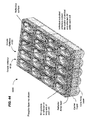
- three different color phosphors that are optically excitable by the laser beam to respectively produce light in red, green, and blue colors suitable for forming color images may be formed on the screen as pixel dots or repetitive red, green and blue phosphor stripes in parallel.
- Phosphor materials are one type of fluorescent materials.
- Various described systems, devices and features in the examples that use phosphors as the fluorescent materials are applicable to displays with screens made of other, optically excitable, light-emitting, non-phosphor fluorescent materials.
- quantum dot materials emit light under proper optical excitation and thus can be used as the fluorescent materials for systems and devices in this application.
- semiconductor compounds such as, among others, CdSe and PbS, can be fabricated in form of particles with a diameter on the order of the exciton Bohr radius of the compounds as quantum dot materials to emit light.
- different quantum dot materials with different energy band gap structures may be used to emit different colors under the same excitation light.
- Some quantum dots are between 2 and 10 nanometers in size and include approximately tens of atoms such between 10 to 50 atoms. Quantum dots may be dispersed and mixed in various materials to form liquid solutions, powders, jelly-like matrix materials and solids (e.g., solid solutions).
- Quantum dot films or film stripes may be formed, oh a substrate as a screen for a system or device in this application.
- three different quantum dot materials can be designed and engineered to be optically excited by the scanning laser beam as the optical pump to produce light in red, green, and blue colors suitable for forming color images.
- Such quantum dots may be formed on the screen as pixel dots arranged in parallel lines (e.g., repetitive sequential red pixel dot line, green pixel dot line and blue pixel dot line).
- Some implementations of laser-based display techniques and systems described here use at least one scanning laser beam to excite color light-emitting materials deposited on a screen to produce color images.
- the scanning laser beam is modulated to carry images in red, green and blue colors or in other visible colors and is controlled in such a way that the laser beam excites the color light-emitting materials in red, green and blue colors with images in red, green and blue colors, respectively.
- the scanning laser beam carries the images but does not directly produce the visible light seen by a viewer. Instead, the color light-emitting fluorescent materials on the screen absorb the energy of the scanning laser beam and emit visible light in red, green and blue or other colors to generate actual color images seen by the viewer.
- Laser excitation of the fluorescent materials using one or more laser beams with energy sufficient to cause the fluorescent materials to emit light or to luminesce is one of various forms of optical excitation, is in other implementations, the optical excitation may be generated by a non-laser light source that is sufficient energetic to excite the fluorescent materials used in the screen.
- non-laser excitation light sources include various light-emitting diodes (LEDs), light lamps and other light sources that produce light at a wavelength or a spectral band to excite a fluorescent material that converts the light of a higher energy into light of lower energy in the visible range.
- the excitation optical beam that excites a fluorescent material on the screen can be at a frequency or in a spectral range that is higher in frequency than the frequency of the emitted visible light by the fluorescent material. Accordingly, the excitation optical beam may be in the violet-spectral range and the ultra violet (UV) spectral range, e.g., wavelengths under 420 nm.
- UV light or a UV laser beam is used as an example of the excitation light for a phosphor material or other fluorescent material and may be light at other wavelength.
- FIGS. 1 and 2 illustrate two laser-based display systems using screens having color phosphor stripes.
- color phosphor dots may also be used to define the image pixels on the screen.
- the system in FIG. 1 includes a laser module 110 to produce and project at least one scanning laser beam 120 onto a screen 101 .
- the screen 101 has parallel color phosphor stripes in the vertical direction where red phosphor absorbs the laser light to emit light in red, green phosphor absorbs the laser light to emit light in green and blue phosphor absorbs the laser light to emit light in blue.
- Adjacent three color phosphor stripes are in three different colors.
- One particular spatial color sequence of the stripes is shown in FIG. 1 as red, green and blue. Other color sequences may also be used.
- the laser beam 120 is at the wavelength within the optical absorption bandwidth of the color phosphors and thus is usually at a wavelength shorter than the visible blue and the green and red colors for the color images.
- the color phosphors may be phosphors that absorb UV light in the spectral range from about 380 nm to about 420 nm to produce desired red, green and blue light.
- the laser module 110 may include one or more lasers such as UV diode lasers to produce the beam 120 , a beam scanning mechanism to scan the beam 120 horizontally and vertically to render one image frame at a time on the screen, and a signal modulation mechanism to modulate the beam 120 to carry the information for image channels for red, green and blue colors.
- Such display systems may be configured, as rear projection systems where the viewer and the; laser module 101 are on the opposite sides of the screen 101 .
- Such display systems may be configured, as front projection systems where the viewer and laser module are on. the same side of the screen 101 .
- FIG. 3A shows an exemplary design of the screen 101 in FIG. 1 .
- the screen 101 may include a rear substrate which is transparent to the scanning laser beam 120 and faces the laser module 110 to receive the scanning laser beam 120 .
- the color phosphor stripes represented by “R”, “G” and “B” for red, green and blue colors are formed on the rear substrate.
- a second substrate, the front substrate, is formed on top of the phosphor stripes and is transparent to the red, green and blue colors emitted by the phosphor stripes.
- the substrate may be made of various materials, including glass or plastic panels.
- Each color pixel includes portions of three adjacent color phosphor stripes in the horizontal direction and its vertical dimension is defined by the beam spread of the laser beam in the vertical direction.
- the laser module 110 scans the laser beam 120 one horizontal line at a time, e.g., from left to right and from top to bottom to fill the screen 101 .
- the laser module 110 is fixed in position relative to the screen 101 so that the scanning of the beam 120 can be controlled in a predetermined manner to ensure proper alignment between the laser beam 120 and each pixel position on the screen 101 .
- FIG. 3A shows the scanning laser beam 120 is directed at the green phosphor stripe within a pixel to produce green light, from that pixel.
- FIG. 3B further shows the operation of the screen 101 in a view along the direction perpendicular to the screen 101 . Since each color stripe is longitudinal in shape, the cross section of the beam 120 may be shaped to be elongated along the direction of the stripe to maximize the fill factor of the beam within each color, stripe for a pixel. This may be achieved by using a beam shaping optical element in the laser module 110 .
- a laser source that is used to produce a scanning laser beam that excites a phosphor material on the screen may be a single mode laser or a multimode laser.
- the laser may also be a single mode along the direction perpendicular to the elongated direction phosphor stripes to have a small beam spread that is confined with the width of each phosphor stripe. Along the elongated direction of the phosphor stripes, this laser beam may have multiple modes to spread over a larger area than the beam spread in the direction across the phosphor stripe.
- This use of a laser beam with a single mode in one direction to have a small beam footprint on the screen and multiple modes in the perpendicular direction to have a larger footprint on the screen allows the beam to be shaped to fit the elongated color subpixel on the screen and to provide sufficient laser power in the beam via the multimodes to ensure sufficient brightness of the screen.
- FIG. 4 shows an implementation of the display in FIG. 1 where a laser source 410 producing the laser beam 120 is directly modulated to carry the image signals in red, green and blue.
- the laser module 110 in this implementation includes a signal modulation controller 420 which modulates the laser source 410 directly.
- the signal modulation controller 420 may control the driving current of a laser diode as the laser source 410 .
- a beam scanning and imaging module 430 is then project the modulated beam 120 to the screen 101 to excite the color phosphors.
- FIG. 5 shows another implementation of the display in FIG.
- a laser source 510 is used to generate a CW unmodulated laser beam and an optical modulator 520 is used to modulate the laser beam with the image signals in red, green and blue.
- a signal modulation controller 530 is used to control the optical modulator 520 .
- an acousto-optic modulator or an electro-optic modulator may be used as the optical modulator 520 .
- the modulated beam from the optical modulator 520 is then projected onto the screen 101 by the beam scanning and imaging module 430 .
- the laser beam 120 is scanned spatially across the screen 101 to hit different color pixels at different times. Accordingly, the modulated beam 120 carries the image signals for the red, green and blue for each pixel at different times and for different pixels at different times. Hence, the modulation of the beam 120 is coded with image information for different pixels at different times to map the timely coded image signals in the beam 120 to the spatial pixels on the screen 101 via the beam scanning.
- FIG. 6 shows one example for time division on the modulated laser beam 120 where each color pixel time is equally divided into three sequential time slots for the three color channels.
- the modulation of the beam 120 may use pulse modulation techniques to produce desired grey scales in each color, proper color combination in each pixel, and desired image brightness.
- FIGS. 7 , 8 , 9 , 10 A and 10 B illustrate examples of some pulse modulation techniques.
- FIG. 7 shows an example of a pulse amplitude modulation (PAM) where the amplitude of the optical pulse in each time slot produces the desired grey scale and color when combined with other two colors within the same pixel.
- PAM pulse amplitude modulation
- the pulse during the red sub pixel time is at its full amplitude
- the pulse during the green sub pixel time is zero
- the pulse during the blue sub pixel time is one half of the full amplitude.
- PAM is sensitive to noise.
- a pulse code modulation (PCM) may be used where the amplitude values of the pulse are digitized. PCM is widely used in various applications.
- FIG. 8 shows another pulse modulation technique where each pulse is at a fixed amplitude but the pulse width or duration is changed or modulated to change the total energy of; light in each color sub pixel.
- the illustrated example in FIG. 8 for the pulse width modulation (PWM) shows a full width pulse in red, no pulse in green and a pulse with one half of the full width in blue.
- PWM pulse width modulation
- FIGS. 10A and 10B illustrate another example of a pulse modulation technique that combines both the PCM and PWM to produce N grey scales.
- the full amplitude of the pulse is divided into M digital or discrete levels and the full sub pixel time is divided into multiple equal sub pulse durations, e.g., M sub pulse durations.
- FIG. 10A shows that a PCM with 16 digital levels and a PWM with 16 digital levels.
- a grey scale may. be achieved by first filling the pulse positions at the lowest amplitude level A 1 .
- FIG. 10B shows one example of a color sub pixel signal according to this hybrid modulation based on PCM and PWM.
- the above hybrid modulation has a number of advantages. For example, the total number of the grey levels is no longer limited by the operating speed or the electronics for PCM or PWM alone.
- the contrast ratio is usually the dominating factor for the contrast ratio. For a given system, the lower the light level of the black color the better the contrast of the display system. Many display systems can achieve a virtual black color by reducing the light levels in all three color sub pixels of a color pixel to their minimum levels without being able to completely shut, off the light.
- the laser-based display systems described here can be designed to completely shut off light in each color sub pixel to produce the true black color. This technique is now described with a specific reference to a diode laser as the light source as an example and it is understood that the technique can also be used in other laser sources.
- a diode laser has a threshold behavior where the laser action starts when the forward driving current is greater than a threshold value and the diode laser emits spontaneously without lasing when the driving current is below the threshold.
- FIG. 11 shows an illustrative optical power as a function of the driving current to a typical diode laser. At a current just below the threshold current, the diode laser emits at a low light level. Hence, the diode laser can be operated at this current level just below the threshold current to produce a virtual black. When a true black is needed, the driving current to the diode laser can be shut off so no light is generated by the laser and no light is generated on the corresponding phosphor stripe in a pixel on the screen.
- diode lasers show a delay behavior where there is a time delay between the optical output and the driving current so that when the driving current is switched on to a value greater than, the threshold value, the laser action lags behind the current for a delay time. This delay is essentially negligible if the initial current is biased just below the threshold current. Accordingly, the diode laser may be operated to produce either the virtual back or the true black depending on the black color distribution in a particular image frame.
- the diode laser When an image frame does not have contiguous black pixels in time less than the delay time of the diode laser, the diode laser is controlled to operate at a bias current just below the threshold current to produce a virtual black in these black pixels.
- the diode laser When an image frame has contiguous black pixels in time greater than the delay time of the diode laser, the diode laser is turned off by shutting off the driving current at the beginning of the black pixels to produce the true black in these pixels. At the end of the this block of contiguous black pixels, the driving current of the diode laser is turned back on to a value just below the threshold current to produce the virtual black for the remaining black pixels so that the first non-black pixel following the block of the contiguous pixels can be timely generated.
- a part of the black pixels is true black and a part of the black pixels is virtual black.
- the light level for the black pixels is better than the virtual black.
- two or more sequential black pixels with a pixel duration of 50 nsec would be sufficient to operate the diode laser to generate the true black.
- FIG. 12 shows a bypass current path for implementing the above technique for generating the true black.
- the bypass current path includes a switch which is normally open so all driving current flow into the laser diode.
- a diode control circuit generates the driving current.
- a display processor which processes the image frames to be displayed and produces the proper control signals for driving the diode laser, sends the control signals based on he image frames to the diode control, circuit.
- the display processor is further connected to a switch control which controls the switch in the current bypass path to turn on the switch when the driving current to the diode laser is to be shut off to generate a true black.
- the display processor monitors the pixels in each image frame to be displayed. This monitoring process can be achieved in the digital domain where the data bits for the pixels in a memory buffer of the processor are monitored. Depending on the length of the contiguous black pixels in time to be displayed, the display processor operates to keep the switch open to produce the virtue black and to close the switch to produce the true black.
- FIG. 13 shows the operation of the display processor.
- the laser module 110 may be fixed in position and orientation relative to the screen 101 in some implementations of the system after the system is assembled. Hence, the relative position of the laser module 110 and the screen 101 is predetermined and pre-calibrated to achieve the pixel registration of the scanning positions of the laser beam 120 on the screen 101 and the pixel positions on the screen 101 .
- This spatial alignment between the laser, module 110 and the screen 101 may change due to various factors. For the screen 101 with parallel color phosphor stripes perpendicular to the horizontal scanning direction, the alignment along the vertical direction is less important than the alignment along the horizontal direction because the former shifts the entire image frame without changing the color registration and the latter, however, changes the color registration and hence degrades the entire image.
- an optical sensing mechanism can be used to detect light from the screen 101 and to detect the horizontal misalignment feedback control may be used to correct the misalignment based on the detected horizontal misalignment.
- the optical sensing mechanism may be built in the screen 101 as a pixel sensor unit.
- FIG. 14 shows an exemplary display system with an on-screen optical sensing unit for optically measuring the responses of color pixels on the screen 101 and a feedback control to allow the laser module 110 to correct the misalignment in response to the feedback signal from the screen 101 .
- the on-screen optical sensing unit may include three optical detectors PD 1 , PD 2 and PD 3 that are respectively configured to respond to red, green and blue light. Each optical detector is only responsive to its designated color and not to other colors. Hence, the red optical detector PD 1 detects only the red light and is not responsive to green and blue light; the green optical detector PD 2 detects only green light and is not responsive to red arid blue light; and the blue optical detector PD 3 detects only the blue light and is not responsive to red and green light This may be achieved by, e.g., using red, green and blue optical bandpass filters in front of the optical detectors PD 1 , PD 2 and PD 3 when each detector may be exposed to light of different colors from the screen 101 , or placing the optical detectors PD 1 , PD 2 and PD 3 in a way that only light of a designated color can enter a respective optical detector for the designated color.
- the red optical detector PD 1 detects only the red light and is not responsive to green and blue light
- the adjacent color phosphor stripes are arranged in the order of red, green and blue from the left to the right in the horizontal direction of the screen 101 . If a red image is generated by the display processor but the red detector does not respond while either the blue detector or the green detector produces an output, the horizontal alignment is out of order by one sub pixel.
- One way to correct this horizontal misalignment is to program the display processor to delay the modulated image signal carried by the modulated laser beam 120 by one sub color pixel time slot, if the green detector has an output and red and blue detectors have no output or by two sub color pixel time slots if the blue detector has an output and red and green detectors have no output.
- This correction of a spatial alignment error by a time delay may be achieved digitally within the display processor.
- No physical adjustment in the optical scanning and imaging units in the laser module 110 is needed.
- the imaging unit in the laser module 110 may be adjusted to physically shift the position of the excitation beam on the screen 101 so that the laser position on the screen 101 is adjusted horizontally to the left or right by one sub pixel in response to the error detected by the on-screen pixel sensor unit.
- the above red, green and blue optical detectors PD 1 , PD 2 and PD 3 may be positioned on the screen 101 to allow each detector to receive light from multiple pixels on the screen 101 .
- a test pattern may be used to check the alignment.
- a frame of one of the red, green and blue colors may be used as a test pattern to test the alignment.
- the red, green and blue optical detectors PD 1 , PD 2 and PD 3 may be embedded in the screen 101 to respectively receive color light from different color sub pixels of one color pixel: FIG.
- FIG. 14A shows a design where three beam splitters BS 1 , BS 2 and BS 3 are placed behind red, green and blue subpixels, respectively and are used to split small fractions of red, green, and blue light beams emitted from the color sub pixels of the color pixel to the three detectors PD 1 , PD 2 and PD 3 formed on the front substrate.
- a testing bit pattern may be used to address that particular pixel to check the horizontal alignment.
- FIG. 15 shows a test pattern for the color pixel embedded with the detectors (top) and the corresponding outputs of the three detectors PD 1 , PD 2 and PD 3 when the horizontal alignment is proper without an error.
- the responses of the three detectors PD 1 , PD 2 and PD 3 are shown as illustrated. Otherwise, different responses will be generated by the three detectors PD 1 , PD 2 and PD 3 and the responses may be used to either use the time-delay technique or the adjustment of the beam imaging optics to correct the horizontal misalignment.
- the sensing of the subpixels for the closed loop: feedback alignment described above may be implemented by an optical sensing unit off the screen 101 .
- FIG. 20A shows one example where three color-selective optical detectors R, G and B for sensing the red, green and blue colors, respectively, are placed away from the screen at a location that can receive the emitted red, green blue light from the screen.
- the above described test pattern for the different colors may be modulated onto the scanning beam to detect the misalignment and the feedback control loop can be used to control the timing of the pulses for the colors to correct the misalignment.
- the present display systems may use a single scanning laser beam 120 to scan one horizontal line at a time to scan through the entire screen 101 .
- multiple lasers such as an array of lasers, may be used to produce multiple parallel scanning beams 120 to divide the screen 101 into N segments along the vertical direction so that one scanning beam 120 is designated to scan one segment and N scanning beams 120 are scanning N different segments at the same time.
- FIGS. 16 and 17 illustrate two display systems with different modulation methods based on the design in FIG. 1 that use multiple scanning laser beams to excite the color phosphor stripes on the screen.
- the horizontal scanning may be achieved with a rotating polygon mirror with M facets and the vertical scanning may be achieved with a galvo mirror.
- the angular ranges for horizontal and vertical scans are similar.
- the segment of 1/12 of a screen is a sub-screen or a screen segment.
- each sub-screen is traced in 1/60 of a second.
- Each M facet moves at a speed of 370 ⁇ sec.
- Each subscreen is scanned twice, one for odd lines and one for even lines in 1/60th second each, this means the galvo mirror moves by discrete steps of 0.3 mrad as shown below:
- Line 1 odd is 0 mrad
- Line 2 odd is 0.3 mrad
- Line 3 odd is 0.6 mrad
- Line 45 odd is 13 mrad
- This type of modulation, frequency can be attained by using an acousto-optic (AO) modulation device. A total of 12 ⁇ 3 UV diode lasers each at about 50-100 mW each may be used to generate the scanning beams.
- FIG. 18 shows one mode of simultaneous scanning of N segments or tiles where N different scanning beams are directed and designated to scan different segments, respectively. Each scanning beam scans its designated segment line by line and is not used to scan in a different segment in producing one full image frame.
- FIG. 19 shows an alternative scanning mode with N scanning laser beams that is described in the U.S. Pat. No. 5,920,361 and can be used with the present display systems. In this mode, N different beams are directed to scan different lines in one segment at the same time and then are directed to scan different lines in the next segment. Hence, each scanning beam is directed to scan different segments in producing one full image frame. Polygons with reflective facets at different angles described in U.S. Pat. No. 5,920,361 can also be used in the present systems.
- each segment of the screen can be driven with a scan engine capable of generating more horizontal lines than actually required for display in that segment (e.g., 4 extra lines).
- the scanning of the system can be configured to have an equal number of extra (unused) lines above and below the segment image. If vertical misalignment exists, the control electronics may shift the segment image upwards or downwards by utilizing these extra lines in place of the normal lines.
- a sensor is required to provide feedback in real time.
- a sensor could be a position sensing diode located to either side of the viewable area of the segment to be controlled.
- the line scans over the sensor.
- a beam splitter may be used to provide feedback while scanning the viewable area of the segment.
- One of the advantages of the above method is to reduce or simplify the requirement for accurate optical alignment because the electronic adjustment, when properly implemented, is simpler to implement and can reduce cost of the device.
- the scan engine for scanning the excitation beam can be rotated slightly. This produces slightly diagonal horizontal scan lines.
- the adjacent screen segments would have scan engines slightly rotated on the opposite direction. Under this condition, to create a straight horizontal line, portions of at least two scan lines are used depending on the amount of the rotation. This may provide a less noticeable junction between the screen segments.
- Another method to reduce the visible junction artifact between two adjacent screen segments is to overlap the colors from each segment at the junction. For example the last blue line of segment #1 may be painted by one of the extra lines from the top of segment #2 by overlapping that extra line with the lasts blue line. Likewise, the first red line of segment #2 may be painted to be one of the extra lines at the bottom of segment #1. This technique can visually spread any junction artifacts.
- FIGS. 20A and 20B show one example of such a system.
- FIG. 20A shows that the screen 2001 with parallel vertical color phosphor stripes includes an array of. cylindrical lenses 2002 that are respectively formed over the individual color phosphor stripes. Each cylindrical lens 2002 covers three adjacent different vertical color phosphor stripes for one color pixel.
- a laser module 2010 produces three different scanning beams at the same wavelength to excite the phosphors on the screen 2001 .
- the three separate scanning beams are directed at three different angles to address three different color sub pixels in each pixel via each of the cylindrical lenses 2002 .
- the three scanning beams may be scanned together or independently to address all pixels. Three separate lasers may be used to generate the three scanning laser beams.
- N sets of the three laser beams may be used to simultaneously scan different screen segments of the screen 2001 in a similar manner as illustrated in FIGS. 16-19 .
- red, green and blue optical sensors may be used to monitor the horizontal alignment between the scanning laser beams and the pixel positions on the screen and a feedback loop may be used to correct the misalignment via either the time delay technique or the adjustment of the imaging optics in the laser module 2010 .
- FIGS. 21A and 21B further show two folded optical designs that direct the output scanning laser beam from the laser module 110 or 2010 to a phosphor color screen in rear projection configurations. At least two reflectors are used to direct the scanning beam along a folded optical path onto the screen. Such folded designs reduce the physical dimension of the systems.
- laser scanning may be achieved by using a combination of a polygon for the horizontal scan and a galvo mirror for the vertical scan.
- a scanning device may be designed to integrate the functions of the polygon and the galvo mirror into a single device.
- FIG. 22 shows one example of such an integrated scanner.
- the scanner includes multiple reflecting facets 2210 around a rotation axis 2230 .
- Each facet 2210 is engaged to a base 2200 via a flexure joint 2220 .
- An actuator 2240 is placed near the top end of each reflecting facet and rotates around the same axis 2230 with its corresponding reflecting facet.
- the actuator is controlled to apply an adjustable force onto the reflect facet to change its titling around the flexure 2220 .
- the actuators 2240 and their corresponding reflecting facets 2210 can be individually controlled to scan the laser beam in the vertical direction while the reflecting facets 2210 rotating around the axis 2230 scan the laser beam in the horizontal direction.
- Two or more actuators 2240 may be provided for each reflecting facet and positioned at different heights along the reflecting surface to gradually tilt the reflecting facet in position for the vertical scanning.
- a single stationary actuator 2240 may be used to control tilting of different reflecting facets 2210 .
- facet 2210 rotates around the axis 2230 and passes by the stationary actuator 2240 , the facet is tilted by the operation of the actuator 2240 to perform the vertical scanning of the beam.
- two or more stationary actuators may be used and placed at different heights of the facets.
- the above scanning-laser display systems with screens having laser-excitable light-emitting materials may be used to form a monochromatic display module by having only one phosphor material on the screen.
- a red monochromatic display module based on this design can be implemented by replacing the green and blue phosphor stripes with red phosphor stripes on the screen 101 in FIG. 1 .
- the scanning laser beam is modulated within the laser module 110 by a monochromatic image signal.
- the image on the screen is red.
- the display resolution of the monochromatic display is tripled.
- Such monochromatic displays can be used to form a color display by combining three monochromatic displays in red, green an blue and projecting the red, green, and blue images to a common “passive” screen that does not emit light to form the final color images.
- the phosphor stripes of the same phosphor material are used here to provide a spatial mask on the phosphor screen to avoid blooming between adjacent pixels.
- Other spatial patterns for the single color phosphor may also be used.
- the monochromatic screen may have a continuous layer of a single color phosphor and use an optional mask on top of the continuous phosphor layer to avoid blooming between adjacent pixels.
- FIG. 23 shows one example of a color laser projector based on the above 3-gun design.
- Red, green, and blue monochromatic display modules are arranged to project red, green, and blue monochromatic images onto and overlap at a common passive display screen to produce the final color images.
- the optical axes of the red, green, and blue monochromatic display modules are arranged relative to one another to converge to the common display screen.
- Each monochromatic display module includes a laser module producing the UV laser beam, modulating the UV laser beam, and scanning the modulated UV laser beam on the corresponding monochromatic phosphor screen to produce images for that color channel.
- the designs in FIGS. 1 and 20A may be used for each, monochromatic display module.
- a channel projection optics module may be placed between the monochromatic phosphor screen and the final common screen to image the monochromatic phosphor screen onto the common display screen.
- a display control is provided to produce the three color channel, control signals to the three laser modules.
- FIG. 24A shows another example of a 3-gun color laser projector using three separate monochromatic display modules to produce colored images on a common passive screen where at least one monochromatic display module directly uses a colored beam to produce a monochromatic color image without the phosphor screen.
- the green and blue monochromatic display modules are based on the scanning-laser display systems with screens having laser-excitable light-emitting fluorescent materials.
- the red display module produces a modulated red laser beam or a red beam from a non-laser light source and directly scans the modulated red laser beam on a screen without the phosphor material.
- the red laser module is different from the green and blue laser modules in this design.
- the red image on the screen in the red display module is projected via its projection optics to the common display screen for displaying the final images. Therefore, the color images on the common display screen are results of mixing phosphor-generated blue and green images with direct red laser images.
- This design can be used to address the current lack of powerful, reliable, efficient, compact, and low cost green and blue solid-state lasers while using the available red solid-state lasers to produce direct red colors.
- FIG. 24B shows another example based on a 3-gun design where both the red and the blue display modules directly scan modulated red and blue laser beams, respectively, on their corresponding projection screens without phosphors to produce red and blue images to be projected onto the final common display screen.
- the green display module uses the scanning UV laser-design With a phosphor-based monochromatic screen based on the designs described in this application such as. the examples shown in FIGS. 1 and 20A .
- a monochromatic laser display module in the above 3-gun color mixing designs may alternatively directly project its scanning laser beam of a desired color to the common display screen without the projection screen. Accordingly, each projection screen without the phosphor material in FIGS. 24A and 24B can be eliminated.
- On the common display screen one or more monochromatic images projected from one or more phosphor projection screens are mixed with one or more monochromatic images directly formed by one or more scanning laser beams at different colors to produce the final images.
- FIGS. 25A and 25B show two examples for this design by modifying the systems in FIGS. 24A and 24B , respectively.
- a red scanning laser beam is directly produced and projected by the red laser module on to the common screen on which the red image scanned out by the red laser is mixed with green and blue images projected from the green and blue phosphor projection screens to produce the final images.
- a red scanning laser beam is directly produced and projected by the red laser module onto the common screen and a blue scanning, laser beam is directly produced and projected by the blue laser module on to the common screen.
- the green, image projected from the green phosphor projection screen is mixed with the direct-scanning laser red and blue images to produce the final images on the common screen.
- the final, common screen for displaying the final images produced common mixing a fluorescence-generated monochromatic image and a monochromatic image at a different color directly formed by a scanning colored beam is an optically “passive” screen in that the screen does not have any fluorescent material that emits light.
- a fluorescence-generated monochromatic image is generated by a phosphor projection screen which is excited by an excitation beam and the image is projected from the phosphor projection screen to the final optically “passive” screen where the mixing with images in other colors occurs.
- the separate projection screens and the final “passive” screen can be replaced by a single screen that generates one or more fluorescence-generated monochromatic images and mixes a fluorescence-generated monochromatic image and a monochromatic image directly formed on the screen by a scanning beam. Because at least one of monochromatic images that form the final image is directly formed on the screen by a scanning beam, the screen in such a design is “partially optically active” in that the screen has a fluorescent material that is excited by an optical excitation beam to produce one or more monochromatic images but does not generate all of the monochromatic images that form the final images on the screen.
- the screen may be designed to include parallel fluorescent stripes and non-fluorescent stripes on a substrate where each non-fluorescent stripe is to display a monochromatic image that is directly formed by diffusing light of a scanning beam without emitting fluorescent light.
- This mixing of one or more direct laser colors with one or more phosphor-emitted colors allows for flexibility in selecting the suitable colored laser sources and fluorescent materials to meet various requirements for different display applications in terms of display performance, display cost, display manufacturing, and other considerations.
- a display system based on this design may include a screen with at least two different fluorescent materials that absorb an excitation beam at an excitation wavelength and emit fluorescent light at two different colors.
- the excitation beam is at a visible color that is different from the colors of the light emitted by the fluorescent materials.
- the screen can include an array of color pixels where each pixel includes subpixels for different colors: a non-fluorescent sub pixel without a fluorescent material to directly display the color and image of the excitation beam, and spatially separated fluorescent subpixels respectively with different fluorescent materials to emit different colors in response to the illumination of the excitation beam.
- the screen can have parallel stripe patterns in a periodic pattern where each period or unit pattern includes a non-fluorescent stripe that does not have a fluorescent material and directly displays the color and image of the excitation beam and adjacent different stripes formed of the different fluorescent materials for different colors.
- the visible monochromatic excitation beam scans through the screen in a direction perpendicular to the stripes to produce different monochromatic images at different colors that form the final colored images on the screen.
- Such an excitation beam may be a single mode laser beam or a multimode laser beam.
- the excitation beam may have a single optical mode in one direction and multiple optical modes in the perpendicular direction to fit to the elongated profile of a color subpixel on the screen and to provide sufficient laser power for desired display brightness.
- FIGS. 26A and 26B show two examples of display systems where the screens have fluorescent regions that emit fluorescent light at different colors under the excitation of a scanning laser beam and non-fluorescent regions that display. images directly, formed by the scanning beam.
- a light module 2601 produces a blue scanning beam to the screen 2601 or 2602 .
- the blue beam is modulated to carry image information in blue and other color channels (e.g., the green and red).
- the image for the blue channel is directly displayed at a non-fluorescent region which diffuses the blue beam to form the blue portion of the final image to the viewer.
- the blue light is incident to the non-fluorescent region from one side of the screen and is diffused by the non-fluorescent screen to merge as diffused blue light on the other side of the screen towards the viewer.
- the fluorescent regions are coated with fluorescent materials that absorb the blue beam and emit light in other color channels to display the images in other color channels, e.g., the green and red phosphor stripes in FIGS. 26A and 26B emit green and red light under excitation by the blue beam.
- the screen 2601 or 2602 is different from other phosphor screens described above and includes repetitive patterns of parallel stripes where each unit pattern includes a red phosphor stripe to emit red light under the excitation of the blue laser 2601 , a green phosphor stripe to emit green light under the excitation of the blue laser 2601 , and a non-fluorescent stripe that diffuses the blue beam to directly display the blue color of the image.
- the blue beam may be at a wavelength around or less than 470 nm.
- each of the screens 2601 and 2602 includes parallel stripe patterns in a period pattern. Each period includes parallel stripes with two fluorescent stripes for the red phosphor and the green phosphor and one non-fluorescent stripe.
- FIG. 26C shows another example of a display system where at least two colors of the three colors for the system are directly produced by two differently colored laser beams on the screen and a third color is produced by the fluorescent emission of a phosphor material on the screen under the optical excitation of the one of the two colored laser beams.
- the illustrated system includes a laser module 2660 to produce two scanning laser beams of two different colors, e.g., a blue laser beam 2630 and a red laser beam 2650 .
- a red laser and a blue laser can be used in the laser module 2650 to produce the two laser beams 2650 and 263 C.
- the red laser beam 2650 is modulated to carry optical pulses with only image information of the red image channel for the display.
- the blue beam 2620 is modulated to carry optical pulses with image information of both the blue image channel and the green image channel and thus, in this regard, is different from the blue laser 2610 in FIGS. 26A and 26B .
- the screen 2603 is different from other phosphor screens including the screens 2601 and 2602 described above and includes repetitive patterns of parallel stripes where each unit pattern 2640 includes a red stripe made of a non-fluorescent stripe to diffuse red light of the scanning red laser 2601 to directly display the red portion of the image, a green phosphor stripe to emit green light under the excitation of the blue laser 2630 , and a blue stripe made of a non-fluorescent stripe that diffuses the blue beam to directly display the blue portion of the image.
- the red stripes and the blue stripes may be made of the same non-fluorescent material or different non-fluorescent materials.
- Each of the two laser beams 2601 and 2630 may be a single mode laser beam or a multimode laser beam.
- each laser beam may have a single optical mode in one direction and multiple optical modes in the perpendicular direction to fit to the elongated profile of a color subpixel oh the screen and to provide sufficient laser power for desired display brightness.
- the material in a non-fluorescent region may be selected to produce a spatial profile including the spatial angular distribution for the diffused light toward the viewer that is substantially identical to or similar to the spatial profile including the spatial angular distribution of the emitted light, toward the viewer from a fluorescent region.
- This feature allows the fluorescent regions and the non-fluorescent regions to have an optically identical or similar appearance to the viewer to ensure the display quality.
- each phosphor region in the screens shown in FIGS. 26A , 26 B and 26 C may emit light toward the viewer in a Lambertian profile.
- each non-phosphor region may be coated with a non-fluorescent light diffusing material that also produces a similar or identical Lambertian profile.
- the non-fluorescent light diffusing material in the non-fluorescent regions may be a uniform binder matrix formed from a binder material with a first index of refraction and particles or clusters of a second material of a second, different index of refraction that are uniformly-distributed or dispersed in the uniform matrix.
- the particles or clusters of a second material diffuse light that is incident to the non-fluorescent from one side of the screen and the diffusion produces output light to the viewer on the other side of the screen.
- the display systems in FIGS. 26A , 26 B and 26 C may also implement an optical sensing unit and a feedback control similar to what is described with respect to. FIGS. 14 , 14 A, 15 , and 20 A.
- the optical sensing unit with red, green and blue detectors which may be on the screen 2603 or off the screen 2603 , can be used to measure the timings of the red, green and blue signals to indicate any horizontal alignment error based on a known, testing pattern modulated onto either the single scanning laser beam 2610 in FIGS. 26A and 26B or the two scanning laser beams 2630 and 2650 in FIG. 26C .
- the feedback, control implemented in the laser module 2660 in response to the output, of the optical sensing unit, can. adjust the timing of the optical pulses to correct the horizontal alignment error on the screen 2603 .
- UV-excitable phosphors suitable of color or monochromatic screens described in this application may be implemented with various material compositions. Typically, such phosphors absorb excitation light such as UV light to emit photons in the visible range at wavelengths longer than. the excitation light wavelength.
- excitation light such as UV light
- red, green, and blue fluorescent materials may be ZnCdS:Ag, ZnS:Cu, and ZnS:Ag, respectively.
- TABLE 1 lists some examples of phosphors that emit visible color light when excited by excitation light in the wavelength range from 380 nm to 415 nm described in various published patent documents. Various phosphors listed in TABLE 1 can also be excited by light from 450 nm to 470 nm. These and other phosphors can be used to implement the phosphor-based laser displays described in this application.
- phosphors described in the published PCT application No. WO 02/11173 A1 are “Type I” phosphors with compositions of Eu-doped photoluminescent metal sulfides in form of MS:Eu where M is at least one of Ca, Sr, Ba, Mg and Zn, and “Type II” phosphors with compositions of metal thiometallate photoluminescent materials in form of M*N* 2 S 4 :Eu, Ce where M* is at least one of Ta, Sr, Ba, Mg and Zn, and N* is at least one of Al, Ga, In, Y, La and Gd.
- a photoluminescent metal sulfide MS (Type I phosphor) may include at least one of Ba, Mg, and Zn alone or in combination with at least one of Sr and Ca.
- a metal thiometallate photoluminescent material may be activated with at least one of europium (Eu) and cerium (Ce).
- Two or more of type I and type II phosphors may be combined, or one or more phosphors of type I and type II phosphors may be combined with other phosphors different from phosphors of type I and type II-to form a phosphor blend to generate a color that may not be available from individual type I and type II phosphors.
- Such type II phosphors emit light in the blue, green or green-yellow spectral range of the visible spectrum.
- the examples of phosphors described in U.S. Pat. No. 6,417,019 include (Sr 1-u-v-x Mg u Ca v Ba x ) (Ga 2-y-z AlIn z S 4 ):Eu 2+ , (Sr 1-u-v-x Mg u Ca v Ba x ) (Ga.sub.2-y-z Al y In z S 4 ):Eu 2+ .
- the phosphor particles may be dispersed in a host material which is selected from, for example, materials including but not limited to epoxies, acrylic polymers, polycarbonates, silicone polymers, optical glasses, and chalcogenide glasses. Alternatively, such phosphors may be deposited on substrate surfaces as phosphor films.
- phosphors described in U.S. Patent Application Publication No. 2002/0185965 include the phosphor powder mixed with the conventional curable silicone composition is a powder of (Y, Gd) 3 Al 5 O 12 :Ce (gadolinium and cerium doped yttrium aluminum garnet) particles available as product number QUMK58/F from Phosphor Technology Ltd., Nazeing, Essex, England. Particles of this phosphor material have a typical diameter of about 5 microns ( ⁇ m), range from 1 to 10 nm, absorb light of wavelengths from about 430 nm to about 490 nm, and emit light in a broad band from about 510 nm to about 610 nm.
- ⁇ m microns
- the color of light emitted by an LED having a stenciled phosphor layer is determined, in part, by the concentration of phosphor particles in the luminescent stenciling composition.
- the phosphor particles may be mixed with the curable silicone polymer composition at concentrations ranging from about 20 grams of phosphor particles per 100 grams of silicone polymer composition to about 120 grams of phosphor particles per 100 grams of silicone polymer composition.
- the titanium dioxide particles may also be used as additives and dispersed in the silicone polymer composition at a concentration of about 1.5 grams of titanium dioxide per 100 grams of silicone polymer composition to about 5.0 grams of titanium dioxide per 100 grams of silicone, polymer composition.
- the titanium dioxide particles which are approximately the same size as the phosphor particles, increase the scattering of excitation light and thus increase the absorption of that light by the phosphor particles.
- finely divided silica particles are dispersed in the mixture to form a thixotropic gel.
- a thixotropic gel exhibits thixotropy, i.e., an apparent drop in viscosity when, subjected to shear and a return to the original viscosity level when the shear force is removed. Consequently, a thixotropic gel behaves as a fluid when shaken, stirred, or otherwise disturbed and sets again to a gel when allowed to stand.
- the silica particles may be, e.g., particles of fumed silica, a colloidal form of silica made by combustion of chlorosilanes in a hydrogen-oxygen furnace.
- Fumed silica is chemically and physically stable at temperatures exceeding 120° C., transparent to visible light, and will impart satisfactory thixotropic properties to the luminescent stenciling composition at comparatively low concentrations.
- the grade of fumed silica used is chosen to be compatible with non-polar materials. In one implementation, the fumed silica is M-5P grade CAB-O-SIL®. untreated amorphous fumed silica obtained from Cabot Corporation of Boston, Mass.
- This grade of fumed silica is hydrophobic and has an average surface area per unit mass of 200 ⁇ 15 m 2 /g.
- the M-5P grade fumed silica particles are dispersed in the mixture of phosphor particles and silicone polymer composition with a conventional three roll mill at concentrations of about 1.5 grams of fumed silica per 100 grams of silicone polymer composition to about 4.5 grams of fumed silica per 100 grams of silicone polymer composition.
- the stenciling composition becomes more thixotropic, i.e. more solid-like as an undisturbed gel.
- fumed, silica having a surface area per unit mass either greater than or less than 200 ⁇ 15 m 2 /g.
- stenciling compositions become more thixotropic as the surface area per unit mass of the fumed silica is increased.
- fumed silicas having lower surface area per unit mass must be used at higher concentrations.
- the required high concentrations of low surface area per unit mass fumed silicas can, result in stenciling compositions having viscosities that are too high to be easily stenciled. Consequently, the fumed silica preferably has a surface area per unit mass greater than about 90 m 2 /g.
- the required concentration of fumed silica decreases, but the fumed silica becomes more difficult to disperse in the silicone polymer composition.
- the examples of phosphors described in the PCT Patent Application Publication No. WO 01/24229 include host materials and dopant ions.
- the host material may have, an inorganic, ionic lattice structure (a “host lattice”) in which the dopant ion replaces a lattice ion.
- the dopant is capable of emitting light upon absorbing excitation radiation. Suitable dopants strongly absorb excitation radiation and efficiently convert this energy into emitted radiation.
- the dopant may be a rare, earth ion which absorbs and emits radiation via 4f-4f transitions, i.e. electronic transitions involving f-orbital energy levels.
- the first and second phosphors comprise a host sulfide material, i.e. a lattice which includes sulfide ions.
- suitable host sulfide materials include CaS, SrS and a thiogallates such as SrGa 2 S 4 .
- a phosphor mixture may be formed by different rare earth ions that are excitable by one common blue energy source of a relatively narrow linewidth to emit light at two different energy ranges (e.g. red and green).
- the dopant is the same in the first and second phosphors with different host materials.
- the red and green emissions of the two phosphors can be tuned by-selecting an appropriate host material.
- the green phosphor is SrGa 2 S 4 :Eu.
- the red phosphor is selected from the group consisting of SrS:Eu and CaS:Eu.
- the examples of phosphors described in U.S. Patent Application Publication No. 2004/0263074 include particles which are characterized as being capable of down-conversion, that is, after being stimulated (excitation) by relatively shorter wavelength light, they produce longer wavelength light (emission).
- the phosphor composition comprises at least one, typically at least two (or three, or four) types of phosphor particles, which each have their own emission characteristics. In an embodiment having at least two different types of phosphor particles, the first type of phosphor particle emits red flight upon excitation, and the second type of phosphor particle emits green light upon excitation.
- typical phosphor particles suitable for use in the phosphor composition may comprise a material selected from SrS:Eu 2+ ; CaS:Eu 2+ ; CaS:Eu 2+ , Mn 2+ ; (Zn, Cd) S:Ag + ; Mg 4 GeO 5.5 F:Mn 4+ ; Y 2 O 2 S:Eu 2+ , MnS:Mn 2+ , and other phosphor materials having emission spectra in the red region of the visible spectrum upon excitation.
- typical phosphor particles suitable for use in the phosphor composition may comprise a material selected from SrGa 2 S 4 :Eu 2+ ; ZnS:Cu,Al arid other phosphor materials having emission spectra in the green region of the visible spectrum upon excitation.
- blue emitting phosphor particles nay be included in the phosphor composition in addition to the red- and green-emitting phosphors; suitable blue emitting phosphor particles may comprise, e.g. BaMg 2 Al 16 O 27 :Eu 2+ , Mg or other phosphor materials having emission spectra in the blue region of the visible spectrum upon excitation.
- the phosphor composition may comprise a type of phosphor particles that is selected to produce yellow light upon excitation.
- phosphor particles suitable, for use in the phosphor composition may include a material selected from (Y, Gd) 3 Al 5 O 12 :Ce, Pr and other phosphor materials having emission spectra in the yellow region of the visible spectrum upon excitation.
- Some suitable red-emitting phosphor particles may have a peak emission wavelength in the range of about 590 nm to about 650 nm.
- the phosphor particles have a peak emission wavelength in the range of about 620 nm to about 650 nm, typically in the range of about 625 nm to about 645 nm, more typically in the range of about 630 nm to about 640 nm.
- the phosphor particles have a peak emission wavelength in the range of about 590 nm to about 625 nm, typically in the range of about 600 nm to about 620 nm.
- the phosphor particles may emit light having a wavelength in the range of about 600 nm to about 650 nm, typically in the range of about 610 nm to about 640. nm, more typically in the range of about 610 nm to about 630 nm.
- Some suitable green-emitting phosphor particles may have a peak emission wavelength in the range of about 52 0 nm to about 550 nm.
- the phosphor particles have a peak emission wavelength in the range of about 530 nm to about 550 nm, typically in the range of about 535 nm to about 545 nm.
- the phosphor particles have a peak emission wavelength in the range of about 520 nm to about 535 nm.
- the phosphor particles emit light having a wavelength in the range of about 520 nm to about 550 nm, typically in the range of about 535 nm to about 550 nm, or in the range of about 520 nm to about 535 nm.
- Some suitable blue-emitting phosphor particles typically have a peak emission wavelength in the range of about 440 nm to about 490 nm.
- the phosphor particles have a peak emission wavelength in the range of about 450 nm to about 470 nm, typically in the range of about 4 55 nm to about 465 nm.
- the phosphor particles have a peak emission wavelength in the range of about 440 nm to about 450 nm, typically in the range of about 4 35 nm to about 445 nm.
- the phosphor particles emit light having a wavelength in the range of about 440 nm to about 430 nm, typically in the range of about 450 nm to about 470 nm.
- Some suitable yellow-emitting phosphor particles typically have a peak emission wavelength in the range of about 560 nm to about 580 nm.
- the phosphor particles have a peak emission wavelength in the range of about 565 nm to about 575 nm.
- the phosphor particles have a peak emission wavelength in the range of about 575 nm to about 585 nm.
- the phosphor particles emit light having a wavelength in the range of about 560. nm to about 580 nm, typically in the range of about 565 nm to about 575 nm.
- the exact wavelength range for each of the above described type of phosphor particles may be determined by selection from available sources of phosphors, desired color attributes of the light emitting device (e.g. the ‘correlated, color temperature’ of the emitted white light), choice of the excitation light such as the excitation wavelength, and the like.
- Useful phosphor materials and other information may be found in Mueller-Mach et al., “High Power Phosphor-Converted Light Emitting Diodes Based on III-Nitrides”, IEEE J. Sel. Top. Quant. Elec. 8(2):339 (2002).
- the examples of phosphors described in the published PCT Application No. PCT/US99/28279 include Ba 2 MgSi 2 O 7 :Eu 2+ ; Ba 2 SiO 4 :Eu 2+ ; and (Sr, Ca, Ba) (Al, Ga) 2 S 4 :Eu 2+ , where the element following the colon represents an activator.
- x, y, and z are all nonzero.
- x and y are both nonzero.
- Examples of green emitting phosphors may have peak emissions between about 500 nm and about 555 nm.
- Ba 2 MgSi 2 O 7 :Eu 2+ has a peak emission at about 495-505 nm, typically about 500 nm
- Ba 2 SiO 4 :Eu 2+ has a peak emission at about 500-510 nm, typically about 505 nm
- (Sr, Ca, Ba) (Al, Ga) 2 S 4 :Eu 2+ has a peak emission at about 535-545 nm, typically about 540 nm.
- phosphors described in U.S. Patent Application Publication No. 2001/0050371 include fluorescent materials that include a CaS phosphor activated by Eu, phosphors represented by AEu (1-x) Ln x B 2 O 8 where A is an element selected from the group consisting of Li, K, Na and Ag; Ln is an element selected from the group consisting of Y, La and Gd; and B is W or Mo; and x is number equal to or larger than 0, but smaller than 1.
- a CaS phosphor activated by Eu or a phosphor of AEu (1-x) Ln x B 2 O 8 may be mixed with a base polymer to form a transparent resin.
- a red phosphor that emits red light may be CaS activated by Eu or a compound expressed by a general formula AEu (1-x) Ln x B 2 O 8 .
- CaS activated by Eu is excited by light of 420 to 600 nm and emits light of 570 to 690 nm which peaks at 630 nm.
- AEu (1-x) Ln x B 2 O 8 is a phosphor which emits light near 614 nm by 5 D 0 ⁇ 7 F 2 transition of Eu 3+ ions.
- the red phosphors can be excited by light near 470 nm (blue) and or 540 nm (green) and can emit light near 620 nm (red).
- x is zero, the phosphor AEuB 2 O 8 is formed and exhibits the highest emission intensity near 615 nm (red).
- a yttrium aluminate phosphor can be a stable oxide having a garnet structure in which Y-atoms of Y 3 Al 5 O 12 are substituted by Gd at part of their positions, particularly a phosphor which is excited by blue light (400 to 530 nm) to emit light of yellow to green region centering 550 nm.
- Activating elements to be added to the yttrium aluminate phosphor include, for example, cerium, europium, manganese, samarium, terbium, tin, chromium, etc.
- Ce Y x Gd 3-x Al 5 O 12 activated by Ce may be used.
- one, two or more kinds of such YAG phosphors may be. mixed together to form. a desired phosphor material.
- the examples of phosphors described, in U.S. Pat. No. 6,252,254 include YBO 3 :Ce 3+ , Tb 3+ ;. BaMgAl 10 O 17 :Eu 2+ , Mn 2+ ; (Sr, Ca, Ba) (Al, Ga) 2 S 4 :Eu 2+ ; and Y 3 Al 5 O 12 :Ce 3+ ; and at least one of: Y 2 O 2 S:Eu 3+ , Bi 3+ ; YVO 4 :Eu 3+ , Bi 3+ ; SrS:Eu 2+ ; SrY 2 S 4 :Eu 2+ , SrS:Eu 2+ , Ce 3+ , K + ; (Ca, Sr) S:Eu 2+ ; and CaLa 2 S 4 :Ce 3+ , where the element following the colon represents an activator.
- the SrS:Eu 2+ , Ce 3+ , K + phosphor when excited by blue light, emits a broadband spectrum including red light and green light.
- These phosphor compositions can be used to produce white light with pleasing characteristics, such as a color temperature of 3000-4100° K., a color rendering index of greater than 70, typically greater than 80, for example about 83-87, and a device luminous efficacy of about 10-20 lumens per watt of input electric power when blue LED is used as the excitation source.
- phosphors described in U.S. Patent Application Publication No. 2002/0003233 include a single crystal Cerium-doped Yttrium-Aluminum-Garnet (Y 3 Al 5 O 12 :Ce 3+ ) compound as a yellowish-light-emitting phosphor.
- Yttrium-Aluminum-Oxides which do not have garnet structures, such as monoklinic YalO and YalO-perovskite, may also be used as the host materials for the phosphors.
- Several lanthanides (Ln) may partly replace the Yttrium, such as in (Y, Ln)AlO, (Y, Ln) (Al, Ga)O.
- the lanthanide may be, for example Lutethium (Lu).
- These host materials may be doped with single dopants such as Cerium (Ce), Praseodymium (Pr), Holmium (Ho), Ytterbium (Yb), and Europium (Eu), or with double dopants such as (Ce, Pr), (Ce, Ho), and (Eu, Pr) to form various phosphors.
- Y 3 Al 5 O 12 :Ho 3+ , and Y 3 Al 5 O 12 :Pr 3+ are examples of single crystal phosphor materials.
- a phosphor listed above emits yellowish light by absorbing either bluish light or ultraviolet light having a wavelength that is shorter than or equal to about 460 nm. In.
- a YAG substrate doped with 4 mol % Cerium (Ce 3+ ) can absorb, light having a wavelength of about 410-460 nm and emit yellowish light having.;,;, a peak wavelength of about 550-570 ⁇ m any.
- Part of the Yttrium in YAG may be substituted by a lanthanide element such, as Gadolinium (Gd).
- a phosphor may be (Y 0.75 Gd 0.25 ) AG:Ce.
- phosphors described in European Patent Application No. 1,150,361 include a resin comprising a phosphor selected from the phosphor family chemically identified as (Sr, Ca,Ba)S:Eu 2+ .
- One phosphor selected from this family is strontium sulfide doped with europium, which is chemically defined as SrS:Eu 2+ and has a peak emission at 610 nm.
- other types of phosphor converting elements may also be used, including phosphor-converting thin films, phosphor-converting substrates, or various combinations of these elements.
- phosphors described in U.S. Patent Application Publication No. 2002/0145685 include a red phosphor SrS:Eu 2+ and a green phosphor SrGa 2 S 4 :Eu 2+ . These phosphors are excitable by the 460 nm blue light.
- the examples of phosphors described in U.S. Patent Application Publication No. 2005/0001225 include rare-earth element doped oxide nitride phosphor or cerium ion doped lanthanum silicon nitride phosphor.
- a rare-earth element doped oxide nitride in the following examples is a crystalline material, not including a glass material such as oxynitride glass. However, it may include a small amount of glass phase (e.g., less than 5%).
- a cerium ion doped lanthanum silicon nitride in the following examples is a crystalline material, not including a glass material.
- One example of a first phosphor is single-phase ⁇ -sialon phosphor that is represented by: Me x Si 12-(m+n) Al (m+n) OnN 16-n Re1 y Re2 z .
- metal (Me) Me is one or more of Li, Ca, Mg, Y and lanthanide metals except for La and Ce
- lanthanide metal Li, Ca, Mg, Y and lanthanide metals except for La and Ce
- Re1 is one or more of Ce, Pr, Eu, Tb, Yb and Er
- Re2 is Dy co-activator.
- Me may be one or more of Ca, Y and lanthanide metals except for La and Ce.
- Me may be Ca or Nd.
- the lanthanide metal (Re1) used for replacing may be Ce, Eu or Yb, In case of using two kinds of metals for replacing, for example, a combination of Eu and Er may be used. In case of using three kinds of metals for replacing, for example, a combination of Eu, Er and Yb may be used.
- the metal (Me) may be replaced by lanthanide metal Re1 and lanthanide metal Re2 as co-activator.
- the lanthanide metal Re2 is dysprosium (Dy).
- the lanthanide metal Re1 may be Eu.
- the metal (Me) replaced by one or more of Ce, Pr, Eu, Tb. Yb and Er (lanthanide metal (Re1)), or one or more of Ce, Pr, Eu, Tb, Yb and Er (lanthanide metal (Me) (Re1)) and Dy (lanthanide metal (Re2)
- the metal is not necessarily added and may be replaced by another metal.
- A-sialon has a higher nitrogen content than oxynitride glass and is represented by: N x Si 12-(m-n) Al (m+n-) O n N 16-n where x is a value obtained dividing (m) by a valence of metal (M).
- oxynitride glass is as described in prior art 3, such a phosphor that serves to shift the position of excitation/emission peak of conventional oxide system phosphors to the longer wavelength side by replacing oxygen atom surrounding the rare-metal element as luminescence-center by nitrogen atom to relax the influence of surrounding atoms to electron of rare-metal element, and that has an excitation spectrum extending until visible region ( ⁇ 500 ⁇ m).
- the metal (Me) is dissolved in the range of, at the minimum, one per three unit cells of ⁇ -sialon including four mass weights of (Si, Al) 3 (N,O) 4 to, at the maximum, one per one. unit cell thereof.
- the solid solubility limit is generally, in case of bivalent metal (Me), 0.6 ⁇ m ⁇ 3.0 and 0 ⁇ n ⁇ 1.5 in the above formula and, in case of trivalent metal (Me), 0.9 ⁇ m ⁇ 4.5 and 0 ⁇ n ⁇ 1.5. It is estimated that, in a region except for those regions, single-phase ⁇ -sialon phosphor is not obtained.
- the interionic distance of lanthanide metal Re1 as luminescence, center to replace part, or all of metal (Me), and to serve as activator is about 5 angstroms at the minimum. It is significantly greater than 3 to 4 angstroms in phosphor known thus far. Therefore, it can prevent a significant reduction in emission intensity due to concentration quenching generated when a high concentration of lanthanide metal as luminescence center is included in matrix material.
- the metal (Me) is replaced by lanthanide metal (Re2) as ⁇ -activator as well as lanthanide metal (Re1) as luminescence center. It is assumed that lanthanide metal (Re2) has two co-activation effects. One is sensitizer function and the other is to newly generate a carrier trap level to develop or improve the long persistence or to improve the thermal luminescence. Since the lanthanide metal Re2 is co-activator, it is suitable that the replacement amount thereof is generally 0.0 ⁇ z ⁇ 0.1 in the earlier formula.
- the single-phase ⁇ -sialon phosphor has ⁇ -sialon as a matrix material, and is essentially different in composition and crystal structure from a phosphor having ⁇ -sialon as matrix material.
- ⁇ -sialon is represented by: Si 6-z Al z O z N 8-z (0 ⁇ z ⁇ 0.2). and it is solid solution of ⁇ -type silicon nitride where part of Si sites, is replaced by Al and part of N sites is replaced by O.
- ⁇ -sialon is represented by: Me x Si 2-(m+n) Al (m+n) O n N 16-n , and it is a solid solution of ⁇ -type silicon nitride, where part of Si—N bonds is replaced by Al—N bond and a specific metal (Me) (Me is one or more of Li, Ca, Mg, Y and lanthanide metals except for La and Ce) invades between lattices and is dissolved therein.
- Me is one or more of Li, Ca, Mg, Y and lanthanide metals except for La and Ce
- a phosphor is synthesized using ⁇ -sialon as matrix material and adding one or more of rare-earth oxides of Ce, Pr, Eu, Tb, Yb and Er as luminescence center, it becomes a mixed material that has a compound including a rare-earth metal between ⁇ -sialon particles since the ⁇ -sialon does not dissolve metal.
- the metal (Me) (Me is one or more of Li, Ca, Mg, Y and lanthanide metals except for La and Ce) is taken and dissolved in the crystal structure and the metal (Me) is replaced by rare-earth metal, Ce, Pr, Eu, Tb, Yb and Er as luminescence center. Therefore, the oxide nitride phosphor composed of single-phase ⁇ -sialon structure can be obtained.
- composition and crystal structure of phosphor drastically changes by whether to use ⁇ -sialon or ⁇ -sialon as matrix material. This is reflected in emission characteristics of phosphor.
- a phosphor that is synthesized adding Er oxide to ⁇ -sialon radiates a blue luminescent light (410-440 nm).
- rare-earth element doped oxide nitride phosphor radiates orange to red light (570-590 nm) due to the activation of Er.
- Er is taken in the crystal structure of ⁇ -sialon and, thereby, Er is influenced by nitrogen atom composing the crystal and therefore, the elongation of light source wavelength, which is very difficult to realize in phosphor with oxide as matrix material, can be easily generated.
- the rare-earth element doped oxide nitride phosphor also has the advantages of matrix material, ⁇ -sialon. Namely, ⁇ -sialon has excellent thermal and mechanical properties and can prevent the thermal relaxation phenomenon that causes a loss in excitation energy. Therefore, in the rare-earth element doped oxide nitride phosphor, a ratio of reduction in emission intensity according to rise of temperature becomes small. Thus, the temperature range available can be broadened as compared to the conventional phosphor.
- the rare-earth element doped oxide nitride phosphor can be excited by ultraviolet rays to X-rays further electron beam, according to O/N ratio in its composition, selection of lanthanide metal Re1 to replace metal (Me), and existence of lanthanide metal Re2 as ⁇ -activator.
- an example of a second phosphor is a rare-earth element doped oxide nitride phosphor that contains ⁇ -sialon as main component (hereinafter referred to as mixture ⁇ -sialon phosphor).
- This second phosphor includes ⁇ -sialon, which dissolves a rare-earth element allowing an increase in brightness of a white LED using blue LED chip as light source, ⁇ -sialon, and unreacted silicon nitride.
- a mixture material with a property equal to single-phase ⁇ -sialon phosphor is found that is composed of ⁇ -sialon that part of Ca site in ⁇ -sialon stabilized by Ca is replaced by one or more of rare-earth metal (M) (where M is Ce, Pr, Eu, Tb, Yb or Er), ⁇ -sialon and unreacted silicon nitride.
- M is preferably Ce, Eu or Yb and further preferably Ce or Eu.
- the mixture ⁇ -sialon phosphor can be produced adding less rare-earth element than the single-phase ⁇ -sialon phosphor. Thus, the material cost can be reduced. Further, since the mixture ⁇ -sialon phosphor also has ⁇ -sialon as matrix material like the single-phase ⁇ -sialon phosphor, it can have the advantages of matrix material ⁇ -sialon, i.e. good chemical, mechanical and thermal properties. Thus, it offers a stable and long-lifetime phosphor material. Due to these properties, it can suppress thermal relaxation phenomenon causing a loss in excitation energy. Therefore, in ⁇ -sialon with dissolved rare-earth element as well as Ca in this embodiment, a ratio of reduction in emission intensity according to rise of temperature becomes small. Thus, the temperature range available can be broadened as compared to the conventional phosphor.
- the mixture ⁇ -sialon phosphor can be excited by ultraviolet rays to X-rays further electron beam, according to O/N ratio in its composition and selection of metal (M).
- the mixture ⁇ -sialon phosphor offers a material that has an emission property equal to the single-phase ⁇ -sialon phosphor even when reducing the amount of rare-earth metal added.
- it is necessary to dissolve more than a certain amount of element.
- amounts of Ca and trivalent metal dissolved are given x and y, respectively, a value of (x+y) is needed to be greater than 0.3 in thermodynamic equilibrium.
- the mixture ⁇ -sialon phosphor includes an organ with ⁇ -sialon and unreacted silicon nitride remained other than single-phase ⁇ -sialon phosphor because of less addition amount and not reaching the thermodynamic equilibrium.
- the amount of added metal in the mixture ⁇ -sialon phosphor is in the range of 0.05 ⁇ (x+y) ⁇ 0.3, 0.02 ⁇ x ⁇ 0.27 and 0.03 ⁇ y ⁇ 0.3 in chemical composition of powder. If the amount of added metal is less than the lower limit, the amount of ⁇ -sialon lowers and the emission intensity lowers. If the amount of added metal is greater than the upper limit, only ⁇ -sialon remains. Therefore, the object of high brightness can be completed.
- the mixture ⁇ -sialon phosphor can be obtained that is composed of: ⁇ -sialon of 40 weight % or more and 90 weight % or less; ⁇ -sialon of 5 weight % or more and 40 weight % or less; and unreacted silicon nitride of 5 weight % or more and 30 weight % or less.
- the reason why the emission intensity is high even with the unreacted silicon nitride included is that ⁇ -sialon epitaxially grows on unreacted silicon nitride and its surface portion mainly responds to excitation light to offer an emission property substantially equal to only ⁇ -sialon.
- the range may be 0.15 ⁇ (x+y) ⁇ 0.3, 0.10 ⁇ x ⁇ 0.25 and 0.05 ⁇ y ⁇ 0.15.
- the mixture ⁇ -sialon phosphor can be obtained that is composed of: ⁇ -sialon of 50 weight % or more and 90 weight % or less; ⁇ -sialon of 5 weight % or more and 30 weight % or less; and unreacted silicon nitride of 5. weight % or more, and 20 weight % or less.
- the mixture ⁇ -sialon phosphor can be obtained by, e.g., heating Si 3 N 4 —M 2 O 3 —CaO—AlN—Al 2 O 3 system mixed powder at 1650 to 1900° C. in inert gas atmosphere to get a sintered body, then powdering it. Since CaO is so instable that it easily reacts with moisture vapor in the air, it is generally obtained by adding in the form of calcium carbonate or calcium hydroxide, then making it CaO in the process of heating at high temperature.
- the chemical composition of mixture ⁇ -sialon phosphor can be defined using the composition range of M- ⁇ -sialon, Ca- ⁇ -sialon and ⁇ -sialon. Namely, in the range of three composition lines of Si 3 N 4 -a(M 2 O 3 .9AlN), Si 3 M 4 -b(CaO.3AlN) and Si 3 N 4 -c (AlN.Al 2 O 3 ), it is defined 4 ⁇ 10 ⁇ 3 ⁇ a ⁇ 4 ⁇ 10 ⁇ 2 , 8 ⁇ 10 ⁇ 2 ⁇ b ⁇ 8 ⁇ 10 ⁇ 2 and 10 ⁇ 2 ⁇ c ⁇ 8 ⁇ 10 ⁇ 1 .
- a third phosphor is a cerium ion doped lanthanum silicon nitride phosphor: La 1-x Si 3 N 5 rxCe (doping, amount x is 0 ⁇ x ⁇ 1), where lanthanum site is replaced in solid dissolution by cerium ion activator. If the doping amount is 0.1 ⁇ x ⁇ 0.5, it is ultraviolet, light excitation phosphor and, if the doping amount is 0.0 ⁇ x ⁇ 0.2, it is electron beam excitation phosphor.
- Lanthanum silicon nitride (LaSi 3 N 5 ) has an excellent thermal stability and serves to suppress the thermal relaxation phenomenon in the process of phosphor emission. Therefore, a loss in excitation energy can be reduced and a ratio of reduction in emission intensity according to rise of temperature becomes small. Thus, in the cerium ion doped lanthanum silicon nitride phosphor, the temperature range available can be broadened as compared to the conventional phosphor. Also, the lanthanum silicon nitride (Lasi 3 N 5 ) has excellent chemical stability and is light resistance.
- the cerium ion doped lanthanum silicon nitride phosphor satisfies a blue chromaticity value and has excellent thermal stability, mechanical property and chemical stability. Therefore, it can have great potential in applications for fluorescent character display tube (VFD), field emission display (FED) etc. that may be used in severe environment.
- VFD fluorescent character display tube
- FED field emission display
- the examples of phosphors described in U.S. Pat. No. 5,998,925 include a garnet fluorescent material comprising 1) at least one element selected from the group consisting of Y, Lu, Sc, La, Gd and Sm, and 2) at least one element selected from the group consisting of Al, Ga and In, and being activated With cerium.
- Y 3 Al 5 O 12 :Ce and Gd 3 In 5 O 12 :Ce are two examples. The presence of Y and Al enables a phosphoer to increase the luminance.
- part of Al may be substituted by Ga so that the proportion of Ga:Al is within the range from 1:1 to 4:6 and part of Y is substituted by Gd so that the proportion of Y:Gd is within the range from 4:1 to 2:3.
- phosphor include (Re 1-r Sm r ) 3 (Al 1-s Ga s ) 5 O 12 :Ce, where 0 ⁇ r ⁇ 1 and 0 ⁇ s ⁇ 1 and Re is at least one selected from Y and Gd.
- a phosphor may include two or more yttrium-aluminum-garnet fluorescent materials, activated with cerium, of different compositions including Y and Al to control the emission spectrum of the phosphor.
- a phosphor may include a first fluorescent material represented by general formula Y 3 (Al 1-s Ga s ) 5 O 2 :Ce and a second fluorescent material represented by the formula Re 3 Al 5 O 12 :Ce, where 0 ⁇ s ⁇ 1 and Re is at least one selected from Y, Ga and La.
- two or more fluorescent materials of different compositions represented by a general formula (Re 1-r Sm r ) 3 (Al 1-s Ga s ) 5 O 12 :Ce, where 0 ⁇ r ⁇ 1 and 0 ⁇ s ⁇ 1 and Re is at least one selected from Y and Gd may be used as the phosphor in order to control the emitted light to a desired wavelength.
- phosphors described in U.S. Pat. No. 6,765,237 include phosphors that absorb UV light from about 3 80 to about 42 0 nm and emit visible light of different colors.
- a phosphor blend may include a first phosphor comprising BaMg 2 Al 16 O 27 :Eu 2+ (BAM) and a second phosphor comprising (Tb.
- A is a member selected from the group consisting of Y, La, Gd, and Sm
- RE is a member selected from the group consisting of Ce, Pr, Nd, Sm, Eu, Gd, Dy, Ho,-Er, Tm, Yb, and Lu
- D is a member selected from the group consisting of Al, Ga, and In
- x is in the range from 0 to about 0.5
- y is in the range from about 0 to about 0.2
- z is in the range from about 4 to about 5.
- a phosphor blend may include a first phosphor comprising Tb 3 Al 4.9 O 12 :Ce and a second phosphor selected from the group consisting of BaMg 2 Al 16 O 27 :Eu 2+ (BAM) and (Sr,Ba,Ca,Mg) 5 (PO 4 ) 3 Cl:Eu 2+
- the phosphors described in U.S. Patent Application Publication No. 2004/0227465 include various phosphor compositions as follows.
- a rare earth element activated complex halide phosphor represented by the formula: BaF 2 .a BaX 2 .bMgF 2 .cBeF 2 .dMe II F 2 :eLn, where X is at least one halogen selected from the group consisting of chlorine, bromine and iodine; Me II is at least one divalent metal selected from the group consisting of: calcium and strontium; Ln is at least one rare earth element selected from the group consisting of: divalent europium (Eu 2+ ), cerium (Ce 3+ ) and terbium (Tb 3+ .), and a is in the range between 0.90 and 1.05, b is in the range of 0 to 1.2; c is in the range of between 0 and 1.2, and d is defined by the sum of c+d being in the range of between 0 and 1.2, and BeF 2 is present in an amount sufficient to effect a phosphor exhibiting a higher luminance than said phosphor absent BeF
- a cerium activated rare earth halophosphate phosphor having the formula: LnPO 4 .aLnX 3 :xCe 3+ in which Ln is at least one rare earth element selected from the group consisting of Y, La, Gd and Lu; X is at least one halogen selected from the group consisting of F, Cl, Br and I; and a and x are numbers satisfying the conditions of 0.1 ⁇ a ⁇ 10.0 and 0 ⁇ x ⁇ 0.2, respectively and exhibiting a higher stimulated emission upon excitation with a He—Ne laser of a wavelength 632.8. nm after exposure to X-rays at 80 KVp, than the phosphor wherein a is less than 0.1. See U.S. Pat. No. 4,661,419 for additional details.
- a mixed single-phase strontium and lanthanide oxide with a magnetolead type crystalline structure having the formula (I): Sr x Ln1 y1 Ln2 y2 Ln3 y3 M z A a B b O 19-k(I) in which Ln1 represents at least one trivalent element selected from lanthanum, gadolinium and yttrium; Ln2 represents at least one trivalent element selected from neodymium, praseodymium, erbium, holmium and thulium; Ln3 represents an element selected from bivalent europium or trivalent cerium with retention of electric neutrality by virtue of oxygen holes; M represents at least one bivalent metal selected from magnesium, manganese, and zinc; A represents at least one trivalent metal selected from aluminum and gallium; B represents at least one trivalent.
- Ln1 represents at least one trivalent element selected from lanthanum, gadolinium and yttrium
- Ln2 represents at least one trivalent
- transition metal selected from chromium and titanium x, y1, y2, y3, z, a, b and k represent numbers so that 0 ⁇ x ⁇ 1, 0 ⁇ y1 ⁇ 1, 0 ⁇ y2 ⁇ 1, 0 ⁇ y3 ⁇ 1, 0 ⁇ z ⁇ 1, 10.5 ⁇ a ⁇ 12, 0 ⁇ b ⁇ 0.5 and 0 ⁇ k ⁇ 1 provided that 0 ⁇ x+y1+y2+y3 ⁇ 1 and that 11 ⁇ z+a+b ⁇ 12. See U.S. Pat. No. 5,140,604 for additional details.
- a divalent europium activated alkaline earth metal halide phosphor having the formula: M II X 2 .aM II X′ 2 .bSiO:xEu 2+ in which M II is at least one alkaline earth metal selected from the group consisting of Ba, Sr and Ca; each of X and X′ is at least one halogen selected from the group consisting of Cl, Br and I, and X is not the same as X′; a and x are numbers satisfying the conditions of 0.1 ⁇ a ⁇ 10.0 and 0 ⁇ x ⁇ 0.2, respectively; and b is a number satisfying the condition of 0 ⁇ b ⁇ 3 ⁇ 10 ⁇ 2 . See U.S. Pat. No. 5,198,679 for additional details.
- a bright, short wavelength blue-violet phosphor for electro luminescent displays comprising an alkaline-based halide as a host material and a rare earth as a dopant. See U.S. Pat. No. 5,602,445.
- the host alkaline chloride can be chosen from the group II alkaline elements, particularly SrCl 2 or CaCl 2 , which, with a europium or cerium rare earth dopant, electroluminesces at a peak wavelength of 404 and 367 nanometers respectively.
- the resulting emissions have CIE chromaticity coordinates which lie at the boundary of the visible range for the human eye thereby allowing a greater range of colors for full color flat panel electroluminescent displays.
- An inorganic thin film electroluminescent device comprising an inorganic light emission layer, a pair of electrodes and a pair of insulating layers, at least one of the electrodes being optically transparent, the light emission layer being positioned between the pair of insulating layers, each insulating layer being formed on an opposite side of the light emission layer, the pair of insulating layers being positioned between a light emission layer and the pair of electrodes, the light emission layer consisting essentially of inorganic material comprising a matrix of lanthanum fluoride doped with at least one member selected from the group consisting of: rare earth element metals and compounds thereof. See U.S. Pat. No. 5,648,181 for additional details.
- a radiographic phosphor screen comprising a support and, coated on the support, at least one layer forming a luminescent portion and an overcoat layer, the luminescent portion and overcoat layer including a binder that is transparent to X-radiation and emitted light and said luminescent portion including phosphor particles in a weight ratio of phosphor particles to binder of 7:1 to 25:1.
- the phosphor comprises oxygen and a combination of species characterized by the relationship: (Ba 1-q M q ) (Hf 1-z-e Zr z Mg e ):yT wherein M is selected from the group consisting of Ca and Sr and combinations thereof; T is Cu; q is from 0 to 0.15; z is from 0 to 1; e is from 0 to 0.10; z+e is from 0 to 1; an y is from 1 ⁇ 10 ⁇ 6 to 0.02. See U.S. Pat. No. 5,698,857 for additional details.
- a garnet fluorescent material comprising: I) at least one. element selected from the group consisting of Y, Lu, Se, La, Gd and Sm; and 2) at least one element selected from, the group consisting of Al, Ga and In, and being activated with cerium.
- a wavelength-converting casting composition for converting a wavelength of ultraviolet, blue or green light emitted by an electroluminescent component, comprising: a) a transparent epoxy casting resin; b) an inorganic luminous substance pigment powder dispersed in the transparent epoxy resin, the pigment powder comprising luminous substance pigments from a phosphorus group having the general formula: A 3 B 5 X 12 :M, where A is an element selected from the group consisting of Y, Ca, Sr; B is an element selected from the group consisting of Al, Ga, Si; X is an element selected from the group consisting of O and S; and M is an element selected from the group consisting of Ce and Tb.
- the luminous substance pigments have grain sizes ⁇ 20 ⁇ m and a mean grain diameter d 50 ⁇ 5 ⁇ m. See U.S. Pat. No. 6,066,861 for additional details.
- UV-excitable phosphors for emitting green, red, and blue colors are Ca 8 Mg(SiO 4 ) 4 Cl 2 :Eu 2+ , Mn 2+ ; Y 2 O 3 :Eu 3+ , Bi 3+ ; and Ba 2 (Sr, Ba, Ca) 5 (PO 4 ) 3 Cl:Eu 2+ (or BaMg 2 Al 16 O 27 :Eu 2+ ); respectively. See U.S. Pat. No. 6,255,670 for additional details.
- the U.S. Patent Application Publication No. 2004/0227465 also discloses phosphors represented by Sr x Ba y Ca z SiO 4 :Eu 2+ in which x, y, and z are each independently any value between 0 and 2, including 0 and 2.
- divalent Eu which serves as an activator, is present in any amount between 0.0001% and about 5% in mole percent based on the total molar weight of said composition.
- the activator, Eu may be present in any amount between. 0.0001% and 5.00% in mole percent based on the total molar weight of the composition, including every thousandth percentage therebetween.
- the parameters x, y and z are 0.5 ⁇ x ⁇ 1.5; 0 ⁇ y ⁇ 0.5; and 0.5 ⁇ z ⁇ 1.5 in the above formula. In yet other implementations, the parameters x, y and z are 1.5 ⁇ x ⁇ 2.5; 0 ⁇ y ⁇ 0.5; and 0 ⁇ z ⁇ 0.5 in the above formula.
- the parameters x, y and z may also be 1.0 ⁇ x ⁇ 2.0; 0 ⁇ y ⁇ 1.0; and 0 ⁇ z ⁇ 0.5 in the above formula.
- the above phosphor Sr x Ba y Ca z SiO 4 :Eu 2+ may further include at least one additional element selected from the group consisting of: Ce, Mn, Ti, Pb, and Sn.
- such an additional element is present in the phosphor in any amount between 0.0001% and 5.00% in mole percent based upon the total molar weight of the phosphor.
- the examples of phosphors described in U.S. Patent Application Publication No. 2005/0023962 include ZnS x Se y :Cu,A in which x and y are each independently any value between 0 and 1 and A is at least one of Ag, Al, Ce, Tb, Cl, I, Mg, Mn.
- the monovalent Cu, which serves as the main activator may be present in any amount between 0.0001% and about 5% in mole percent based on the total molar, weight of said composition.
- the activator, Cu may be present in any amount between 0.0001% and 5.00% in mole percent based on the total molar weight of the composition, including every thousandth percentage therebetween.
- the parameters x, y and z are 0.5 ⁇ x ⁇ 1 and 0 ⁇ y ⁇ 0.5 in the above formula. In other implementations, the parameters x, y and z are 0 ⁇ x ⁇ 0.5 and 0.5 in the above formula. The parameters x, y and z may also be 0 ⁇ x ⁇ 0.5 and 0.5 ⁇ y ⁇ 1.0 in the above formula.
- phosphors described in U.S. Patent Application Publication No. 2005/023963 include thioselenide and/or selenide-based fluorescent-materials which are capable of absorbing with high efficiency blue, violet, or ultraviolet (UV) light and emitting light of a wavelength longer than that absorbed from the light source.
- phosphor materials may be manufactured to emit broad color spectra that can be tuned, from blue to green to yellow and red emissions. Two or more phosphors may be mixed in order to achieve a specific, desired white color performance.
- the divalent Eu which can serve as the main activator, may be present in any amount between 0.0001% and about 10% in mole percent based on the total molar weight of said composition.
- the activator, Eu may be present in any amount between 0.0001% and 10.00% in mole percent based on the total molar weight of the composition, including every thousandth percentage therebetween.
- the parameters x, y, and z are 0.5 ⁇ x ⁇ 1 and 0 ⁇ y ⁇ 0.5 in the above formula.
- the parameter x, y and z are 0 ⁇ x ⁇ 0.5 and 0.5 ⁇ y ⁇ 1.0 in the above formula.
- x is about 0 and y is about 1 in the above formula, or x is about 1 and y is about 0 in the above formula.
- the divalent Eu which can serve as the main activator, may be present in any amount between 0.0001% and about 10% in mole percent based on the total molar weight of said composition.
- the activator, Eu may be present in any amount between.
- M1 comprises an element selected from the group consisting of: Be, Mg, Ca, Sr, Ba, Zn
- M2 comprises an element selected from the group consisting of: Be, Mg, Ca, Sr, Ba, Zn
- A comprises one or more elements selected from the group consisting of: Al, Ga, In, Y, La, and Gd
- B comprises one or more elements selected from the group consisting of: Eu, Ce, Cu, Ag, Al, Tb, Cl, Br, F, I, Mg, Pr, K, Na, and Mn.
- B may be present in any amount between 0.0001% and about 10% in mole percent based on the total molar weight of said composition, and wherein x and y are each independently any value between 0 and 1, subject to the provisos that the sum of x and y is equal to any number in the range of between about 0.75 and about 1.25, the sum of m and n is about 1, and M1 is different than M2.
- the parameters x and y are 0 ⁇ x ⁇ 1 and 0 ⁇ y ⁇ 0.5 in the above, formula.
- the parameters x and y are 0 ⁇ x ⁇ 0.5 and 0 ⁇ y ⁇ 0.5, or 0 ⁇ x ⁇ 0.5 and 0.5 ⁇ y ⁇ 1.0, or x is about 0.75 and y is about 0.25, or x is about 0 and y is about 1, or x is about 1 and y is about 0, in the above formula.
- M1 comprises an element selected from the group consisting of: Be, Mg, Ca, Sr, Ba, Zn
- M2 comprises an element selected from the group consisting of: Be, Mg, Ca, Sr, Ba, Zn
- A comprises one or more elements selected from the group consisting of: Al, Ga, In, Y, La, and Gd
- 3 comprises one or more elements selected from the group consisting of: Eu, Ce, Cu, Ag, Al, Th, Cl, Sr, F, I, Mg. Pr, K, Na, and Mn.
- B may be present in any amount between 0.0001% and about 10% in mole percent based on the total molar weight of said composition, and wherein x and y are each independently any value between 0 and 1, subject to the provisos that the sum of x and y is equal to any number in the range of between about 0.75 and about 1.25, the sum of m and n is about 2, and M1 is different than M2.
- the parameters x and y are 0.5 ⁇ x ⁇ 1 and 0 ⁇ y ⁇ 0.5 in the above formula.
- the parameters are 0 ⁇ x ⁇ 0.5 and 0 ⁇ y ⁇ 0.5, or 0 ⁇ x ⁇ 0.5 and 0.5 ⁇ y ⁇ 1.0, or x is about 0.75 and y is about 0.25, or x is about 0 and y is about 1, or x is about 1 and y is about 0 in the above formula.
- the color generation is based on mixing of three primary colors of red, green, and blue.
- the described devices, systems, and techniques may use mixing of four or more colors to generate the desired colors.
- four different colors may be used.
- the screens shown in FIGS. 1 and 2 use four different color phosphor stripes and each color pixel includes four sub color pixels.
- the display systems in FIGS. 23-25 under this 4-color scheme can use four monochromatic laser display modules in four different colors to produce the final color images on the common display screen.
- a phosphor screen which may be used as either a projection screen as shown in FIGS. 23-26B or a final viewing screen as shown in FIGS.
- fabrication techniques include, among others, the following: inkjet printing, painting, gravity settling, settling with compression, slurry, slurry with segregation, dusting, photo-tacky dusting; thin screen evaporation and sputtering, screen printing, pressed printing, pulsed laser deposition, centrifugal deposition, electrophoretic deposition, spraying, electrostatic dusting, tape transfer, reactive deposition, reactive evaporation, RF sputtering with ion implantation of activators, metal organic chemical vapor deposition (MOCVD), and atomic layer epitaxy.
- MOCVD metal organic chemical vapor deposition
- the painting techniques apply luminescent paints on a substrate, such as fluorescent, phosphorescent and self-luminous painting materials. Paints can be organic or inorganic in nature and are used with a vehicle such as lacquers or oils. Paints can be applied with a brush, roller or a spraying device. Stencils may be used to obtain detailed spatial patterns. Paints can also be applied via off-set printing methods. These fluorescence and phosphorescent paints can be excited via IR, visible or UV radiation. In the self luminous paints the source of the excitation is a radioactive material (ex. Radium) mixed with the paint.
- a radioactive material ex. Radium
- settling of phosphor slides may be achieved with a mixture of phosphor, a 1% barium acetate solution (in water), PS-6 potassium silicate and deionized water in a settling chamber.
- One recipe is to add 34 ml of the 1% barium acetate to the settling chamber.
- N. Yocom in the 1996 SID Seminar on Phosphor Screening discussed nine steps for settling and aluminizing a phosphor screen which are 1. settle phosphor on a face plate, 2. a liquid cushion is decanted and siphoned off, 3. dry the settled screen, 4. bake the screen, 5. rewet the screen, 6. apply a filming material on top of water, 7. remove water, 8. evacuate and evaporate the aluminum layer. 9. bake the screen.
- the slurry methods use a phosphor-containing slurry to form a phosphor layer over a screen surface. See, e.g., Tatayama, Yamazaki, Kato & Tashima, European Patent Application #86302192.9, filed Mar. 25, 1986 by Sony.
- One of his recipes is to use 100 g of phosphor, 0.6 g of Aerosil, with 5 g of PVA and 0.5 g of ADC (ammonium dichromate) and 100 g of water to form the slurry.
- This slurry is then deposited near the center of the face of a CRT screen panel and the panel is rotated and tilted to spread the slurry over the inside of the face plate.
- a cascaded slurry system may be used an aging effect where the silicate concentration is set to be higher on the glass substrate side than that on the electron gun side.
- 3,025,161 entitled “Method of Forming Patterns” and issued Mar. 13, 1962 discloses a dusting method where the phosphor is dusted more vigorously via a dry powder spray system onto a wet photo-resist prior to exposure.
- phosphors are dusted on photo-tacky, coated dry surface and are exposed UV to allow the coating to become tacky.
- This tacky nature of the surface coating causes the phosphor in the exposed areas to be attached to the surface. See, Nonogaki, Tomita, Nishizawa, Akagi & Kohasji, “Dry Process for Phosphor Screen Fabrication of Multicolored Cathode Ray Tubes,” Research &. Development in Japan, 1984, pp. 50-55.
- Phosphor screens can also be made by settling the phosphors with compression. See, e.g., Cki K. & Ozawa L., A phosphor screen for high-resolution CRTs, Journal of the SID, Vol. 3, No. 2, September 1995, pp. 51-57 which describes settling with normal sedimentation techniques and a use of a mechanical press machine to reduce the voids in the screen for high resolution uses.
- High resolution screens can be made by evaporating or sputtering the phosphor on the substrate.
- magnetron sputtering of ZnGa 2 O 4 onto BaTiO 3 ceramic sheets have been used in thin film Electro-luminescent devices.
- Vacuum evaporation methods have been used to deposit a thin layer of phosphor on a substrate such as a SrS:Ce, Cl, Ag, Mn layer.
- Phosphor screens can also be made by screen printing, techniques.
- a tight but spring-like cloth or metal mesh is used with areas blocked by a lacquer and aligned above a substrate to be coated.
- the slurry mix is then mechanically pressed through the selected areas of the mesh on to the substrate and the mesh springs back to its original position after the phosphor paste is applied.
- photographic printing of patterns on a mesh very fine patterns, can be screen printed.
- Morikawa et al discussed a method to achieve a smoother and better aging screen using a printing method plus screen compression. This compression method allows the manufacturer to achieve higher packing densities. See, Morikawa, Seko, Kamogawa & Shimojo, Study to Improve Flood Beam CRT for Giant Screen Display, Japan Display '92, pp 385-388.
- Laser pulses can be directed to target materials and deposit the target materials on a screen.
- Greer et al in 1994 reported a Pulsed Laser Deposition (PLD) of phosphor screens used in helmet mounted displays (HMD). See, Greer, J. A. et al., P-53 Thin Film Phosphors Prepared by Pulsed—Laser Deposition, SID 94 Digest, pp. 827-830.
- a rastered laser with a wavelength of 248 nm was used to scan targets of Yttrium Aluminum Gallium Garnet phosphors and to deposit these materials on to sapphire substrates by ablation.
- a screen growth rate of one micron per hour and screens of a thickness up to 8 microns were reported.
- a phosphor suspension in a solution can be deposited on a screen by using a centrifugal action. See, e.g., Mezner, L. Z., Zumer, M., Nemanic, V., Centrifugal Settling of High Resolution 1-in CRT Screens, SID Digest 1994, pp 520-522.
- CRT screens have been made by this method where, a stable phosphor suspension is made with a fine grain (less than 5 micron particle size) phosphor, a binder, electrolyte and in some cases a dispersing agent.
- the settling in the centrifuge may be set at 3000 rpm for 2 minutes to 4000 rpm for 3 minutes.
- Electrophoretic or Cataphoretic phosphor coatings can be used to make high resolution phosphor screens.
- Schesinger described an electrophoretic coating process where a conductive coated glass face plate is put in a solution of a phosphor and electrolyte and a metallic anode (situated about two inches from the face plate). Sclesinger et al., Design Development and Fabrication of Ultra High-Resolution Cathode Ray tube. Technical Report ECOM-00476-February 1969, pp 64-72. When a DC electric current of 20 ma is passed through the solution the phosphor screen is deposited on the cathode.
- wet or dry phosphors can be sprayed on a substrate to form a phosphor screen.
- the nozzle of the spray gun can be changed to spray at various spray angles depending on the distance from the substrate and other constraints.
- a pressure pot is used as in various spray systems to keep the pressure constant to the spray gun.
- the dry phosphor is sprayed on the screen face whose surface is coated with an adhesive binder, wet binders and dry binders can be used.
- an organic binder ouch as nitrocellulose or PVA may be used.
- a binder which becomes tacky under UV radiation bombardment may also be used.
- Phosphor screens can also be made by using a phosphor spray or dusting process in which the phosphor is charged and blown against a charged screen surface. The phosphors are then fixed to allow further processing.
- the U.S. Pat. No. 5,477,285 entitled “CRT developing apparatus” and issued Dec. 19, 1995 describes a process where a tribo-electric gun is used to charge the phosphor, and the phosphor is fed to the panel using a hopper, an auger to transfer the material from the hopper to the venturi chamber. The venturi chamber dispenses the charged phosphor to the latent image on the panel.
- the phosphor is coated on a tape base with a layer to contain phosphor. Under the phosphor layer is a release layer and the phosphor and binder are pressed onto a substrate. The base tape is removed, leaving the phosphor and binder. See, N. Yocom—0.1996 SID Seminar on Phosphor Screening.
- Vapor reaction processes can be used for fabricating phosphor layers such as ZnS phosphor layers. See, e.g., D. A. Cusano, Cathodo-, Photo-, and D.C-, Electro-luminescence in Sine Sulfide Layers. Luminescence of Organic and Inorganic Materials Edited by Kallman & Spruch Wiley Sons 1962, pp 494-522.
- the substrate to be coated can be heated to temperatures from 400-700 deg C.
- materials Zn, ZnCl 2 , MnCl 2 .H 2 S are continuously present during the formation of the phosphor layer. This, process can also be used for fabricating electroluminescent screens.
- Transparent thin films of Y 2 O 2 S:Eu have been formed by a reactive evaporation process where the Yttrium metal is evaporated onto a substrate using an electron beam gun and excited SO 2 is introduced while simultaneously heating a crucible of EuCl 2 powder.
- RF sputtering and ion implantation for forming phosphor screens
- the activator ion is implanted.
- N. M. Kalkhoran et al. Luminescence Study of Ion-Implanted, ZnGa 2 O 4 Thin Films on Flexible Organic Substrates, SID '97 Digest, pp 623-626
- RF sputtering was used to form thin film electroluminescent screens where ZnGa 2 O 4 thin films were implanted on a flexible polyimide substrate with Mn, Eu to get green and red phosphor screens.
- the un-doped host material was. used for the blue screen.
- MOCVD Metal Organic Chemical Vapor Deposition
- CaGa 2 S 4 :Ce phosphor a MOCVD process for fabricating screens with the CaGa 2 S 4 :Ce phosphor was reported by Smith et. Al., in “Crystalline-As-Deposited CaGa2S4:Ce via Low Temperature Metal Organic Chemical Vapor Deposition”:SID Digest 1995, Vol. XXVI pp 728-731.
- Calcium metal-organics were used in the form of Ca(2,2,6,6-tetramethyl-2,5-heptanedionate) 2 called Ca(thd) 2 .
- the CaS was deposited using Ca(thd) 2 in an argon carrier gas and H 2 S.
- Atomic layer epitaxy has been used to form luminescent screens for alternating current thin film electroluminescent displays. See, Lindsay McDonald and Anthony Lowe, Display Systems, Publisher John Wiley & Sons 1997 pp. 195 & 196.
- a substrate was heated to a high temperature (500° C.) and was exposed to low pressure chemical precursors for forming the screen layers.
- Zn and Mn can be used as part of the precursors for forming a ZnS:Mn layer.
- the reactor is evacuated and Sulfur is introduced.
- the epitaxy cycle is then started to form the layers.
- the phosphor materials used for screens described in this application may be prepared as phosphor nanoscale powders where in the phosphor materials are nanoscale particles or grains of 500 nm or less to produce enhanced optical conversion efficiency.
- Such phosphor nanoscale powders may be prepared by forming a solution or slurry which comprises phosphor precursors and then firing the solid residue of the solution or slurry which comprises the phosphor precursors.
- the phosphor precursors in the form of nano-sized particles or grains have a dimension less than 500 nm, preferably 200 nm or less, more preferably 100 nm or less, even more preferably 50 rim or less, and most preferably 10 nm or less.
- the nano-sized particles may have an average particle size of in the range from 1 nm to 500 nm, preferably 2 nm to 200 nm, more preferably 2 nm to 100 nm, even more preferably 2 nm to 50 nm, most preferably 3 nm to 10 nm.
- the nano-sized particles of the precursor will also preferably have a uniform size distribution, with a variation within a range, e.g., 10% or less.
- U.S. Pat. No. 6,576,156 which is incorporated by reference, in its entirety as part of this application, describes examples of phosphor nanoscale powders and fabrication techniques.
- phosphor nanoscale powders may be prepared by (1) forming, a solution or slurry which contains nanosized particles of the phosphor precursors, (2) drying the solution or slurry to obtain a residue; and (3) firing the residue to form a phosphor nanoscale powder.
- a screen suitable for use in the devices of this application may include one or more fluorescent materials to form a fluorescent layer sandwiched between two dichroic layers D 1 and D 2 to receive excitation laser light through the first dichroic layer D 1 and the emitted colored light from the fluorescent layer exits the screen via the second dichroic layer D 2 .
- the first dichroic layer D 1 is designed to transmit the excitation laser light, e.g., UV light, and to reflect visible light.
- the second dichroic layer D 2 is designed to be complementary to the layer D 1 : transmits visible light and reflects the excitation laser light, e.g., UV light.
- This screen design with the two dichroic layers D 1 and D 2 can effectively confine the excitation light such as UV light within the fluorescent layer so that the unabsorbed excitation light after passing through the fluorescent layer is reflected back by the dichroic D 2 layer to continue interacting with the fluorescent materials to improve the utility efficiency of the excitation light.
- the visible light by the fluorescent layer which originally tends to be in all directions, is directed by the dichroic D 1 layer towards the viewer aide of the screen to be viewed by a viewer without leaking to the back of the screen. Accordingly, the overall utility efficiency of the emitted light and the brightness of the screen are enhanced.
- FIGS. 27A and 27B illustrate two examples based on the above screen design.
- a substrate is provided to support the dichroic layers D 1 , D 2 and the fluorescent layer.
- FIG. 27A shows an example in a surface incident configuration where the substrate is on the side of the D 2 layer and the emitted light exits the screen through the substrate. This configuration provides better transmission properties for the excitation light such as UV light, a minimum back reflection towards the excitation laser, and allows the substrate side to act as a shield from the user interface side.
- FIG. 27B shows an example in a substrate-side-incident configuration where the substrate is on the side of the D 1 layer and the incident excitation laser light enters the screen through the substrate.
- the UV laser light may be at around 405 nm.
- the D 1 layer reflects visible light with a wavelength greater than 430 nm and transmits UV light with a wavelength shorter than 415 nm or 400 nm.
- the D 2 layer reflects UV light with a wavelength shorter than 415 nm or even less than 400 nm and transmits visible light with a wavelength greater than 430 nm.
- Anti-reflection (AR) coatings may be used to further enhance the efficiency of the screen.
- the substrate-side-incident configuration allows the substrate to be treated to form an optical diffractive or “power” element (e.g., a Fresnel lens) and provides better transmission of the colored light to the viewer side.
- a hard protective surface may be formed on the viewer or user side of the screen to protect the screen.
- TABLE 2 shows the examples of 6-layer screens where S represents the substrate, one or more phosphors are used to form the fluorescent layer and a lacquer layer (L) or other capsulation layer is used to protect the overall screen structure from handling and environmental conditions.
- the substrate may be made out of a plastic or glass material that is capable of transmitting light in the spectral range of the visible light, e.g., 400-800 nm.
- FIG. 27C shows an exemplary transmission spectrum of the D 1 layer.
- FIG. 27D shows the absorption and emission spectra of a phosphor which can be used as part of the fluorescent layer.
- the phosphor layer may be a striped phosphor capable of fluorescing when excited by a violet or UV-source.
- FIG. 27E shows the transmission spectrum of the layer D 2 .
- FIG. 27F further shows the reflective spectrum of the AR coating capable of improving the transmission of visible light in the range of, e.g., between 400-800 nm.
- a black matrix may be formed in the phosphor layer to separate two adjacent phosphor stripes and to reduce the smearing at a boundary between two adjacent subpixels within one color pixel and two adjacent color pixels where each color pixel in this, example includes red, green and blue subpixels.
- the black matrix includes an absorptive or reflective wall to surround the phosphor area of each stripe in order to confine the light emitted by that phosphor, from spreading into neighboring phosphors that emit different colors.
- Such pixelation can be accomplished by spin coating a photo resist on the substrate and etching away the desired sub-pixel geometry which is filled via screen printing by the corresponding phosphor.
- the black matrix can be implemented in vertical only shape or square shaped (i.e. both vertical and horizontal lines).
- the excitation laser light in the above described systems may enter the fluorescent layer of the screen at an angle due to the scanning action of a beam scanning module to scan the excitation beam across the screen.
- This incident angle varies with the entry position of the laser light.
- the direction of the laser light should be as close to the normal direction to the fluorescent, layer as possible to improve the image quality.
- an optical mechanism may be implemented at the entry to the screen to direct the incident laser beam to be normal or approximately normal to the screen.
- a Fresnel lens which is constructed as a layer of the screen, to make the incident laser light approximately normal to the screen.
- FIG. 28 shows an example of a screen with a Fresnel lens layer formed at the entry side of the fluorescent layer of the screen.
- the Fresnel lens is formed in a dielectric substrate that may be made of, e.g., a glass or a plastic material.
- An acrylic plastic material for example, may be used to form the Fresnel lens layer.
- a gap or an optical material with a different index than the Fresnel lens layer may be used to create a difference in the refractive index from the Fresnel lens to the next layer of the screen.
- an anti-reflection layer at the entrance surface of the screen for receiving the excitation laser light may also be formed in the screen, such as an anti-reflection layer at the entrance surface of the screen for receiving the excitation laser light, and a dichroic filter layer D 1 on the laser-entry side of the fluorescent layer.
- a dichroic filter layer D 1 on the laser-entry side of the fluorescent layer.
- an encapsulation layer, a screen gain layer, a contrast enhancing layer, and a second dichroic layer D 2 (a UV blocker) may also be provided in the screen.
- the first dichroic layer D 1 is designed to transmit light from 405 nm to 410 nm with a transmission of about 99.75% and to reflect visible light from 440 nm to 410 nm with a reflectivity of about 95%; the anti-reflection layer is designed to transmit UV light at 405 nm with a transmission of about 99.75%.
- the screen gain layer is designed to optically enhance the brightness and viewing angle of the screen and may include a lenticular layer with lens elements, a diffractive optic layer of diffractive elements, a holographic layer with holographic elements, or a combination of these and other structures.
- the contrast enhancing layer may include a color-selective absorbing pigment in each subpixel to absorb ambient light and to transmit light in the color of that subpixel.
- the order of the encapsulation layer, the screen gain layer, the contrast enhancing layer and the UV-blocking D 2 layer may vary with screen designs.
- FIG. 29 illustrates the operation of the Fresnel lens layer in FIG. 28 .
- the Fresnel lens has Fresnel rings and can be configured to redirect the incident laser light via optical diffraction, refraction or both.
- the Fresnel lens can be in a telecentric configuration for the incident scanning laser light. Since the Fresnel lens is to redirect the incident laser light at any entry angle to be approximately normal to the screen, the Fresnel lens can be placed at different layer positions on the laser-entry side of the fluorescent layer of the screen.
- FIG. 30 shows an example of a screen based on the design in FIG. 28 with additional details on the various layers such as the black matrix layer with “black” dividers between different phosphor sub pixels to reduce the color mixing or cross talk, a gain layer for enhancing the brightness and increasing the viewing angle, and a contrast enhancing layer to reduce the reflection of the ambient light to the viewer.
- the “black” dividers between different fluorescent regions are used to in part, to separate mixing of adjacent fluorescent regions and may be implemented in various configurations.
- the dividers may be optically reflective to reflect emitted colored light at large angles within a fluorescent region and therefore such dividers can act as a “light pipe” to improve directionality of each emitting fluorescent region.
- the dividers may also be optically absorbent to absorb the emitted colored light at large angles.
- the dividers may be physical grooves formed at the boundaries of different phosphor regions.
- FIG. 31 further shows an example of a screen with two dichroic layers in which different phosphors for different colors are formed at different layers and do not overlap with one another.
- each layer includes patterned phosphor regions of the same phosphor for one color and non-phosphor regions with a filler material.
- the dividers for reducing color crosstalk may be physically printed with color phosphors, or contained in separate layers.
- the multi-layer structure of the fluorescent layer may be implemented in different configurations.
- a host substrate can be used to support different phosphors where non-overlapping phosphor patterns are coated on either side of the substrate. This, design of the phosphor layers allows different phosphor layers to be individually fabricated and laminated together by, e.g., using a suitable optical adhesive or an optical pressure-sensitive film.
- FIG. 32 shows an example of sidewall reflector stripes formed between different phosphor stripes to physically separate the different phosphor stripes so that light of different colors emitted by different phosphors can be optically separated to reduce color mixing or cross talk.
- a substrate is provided and different phosphor stripes are formed on the substrate.
- the substrate is structured to have raised walls or lands to physically divide the substrate surface into different stripes and can also provide a control means for controlling the amount of a phosphor during the application, of the phosphors into the stripes.
- the raised walls block the cross talk between two adjacent phosphor stripes of different colors.
- Each of the above dichroic layers used in the screens may be implemented in various configurations. For large format displays, it may be desirable that such a dichroic layer be made of relatively inexpensive materials and be relatively easy to manufacture.
- Multiple dielectric layers can be designed to construct various wavelength-selective optical filters by controlling the refractive indices and the physical thickness values of the layers. For example, multiple layers of alternating high and low index dielectric layers may be designed to achieve desired wavelength-selective reflection and transmission spectra.
- Two different multi-layer sheet materials may be used as the D 1 and D 2 dichroic layers for the UV-phosphor color screens described in this application, e.g., the designs in FIGS. 27A through 32 .
- multiple sheets of films with different refractive indices may be laminated or fused together to construct a composite sheet as the D 1 or D 2 dichroic layer.
- multiple layers of two different materials with different indices may be used to form a composite film stack as D 1 or D 2 by placing the two materials in an alternating manner.
- three or more different materials with different indices may be stacked together to form the composite film stack as D 1 or D 2 .
- Such a composite sheet for the D 1 layer is essentially, an optical n interference reflector that transmits the excitation light (e.g., UV light) that excites the phosphor materials which emit colored visible light and reflects the colored visible light.
- a composite sheet for the D 2 layer may be complementary to the D 1 layer transmitting the colored visible light emitted by the phosphors and reflecting the excitation light (e.g., UV light).
- Such composite sheets may be formed of organic, inorganic or a combination of organic and inorganic materials.
- the multiple-layer composite sheet may be rigid or flexible.
- a flexible multi-layer composite sheet may be formed from polymeric, non-polymeric materials, or polymeric and non-polymeric materials. Exemplary films including a polymeric and non-polymeric material are disclosed in U.S. Pat. No. 6,010,751 entitled “Method for forming a multicolor interference coating” and U.S. Pat. No.
- 6,531,230 is incorporated by reference as part of the specification of this application.
- the use of polymer pairs having high index differentials allows the construction of very thin, highly reflective mirrors that are freestanding, i.e. have no substrate but are still easily processed for constructing; large screens.
- Such a composite sheet is functionally a piece of multi-layer optical film (MOF) and includes, e.g., alternating layers of PET and co-PMMA to exhibit a normal-incidence reflection band suitable for the screen applications of this application.
- MOF multi-layer optical film
- ESR enhanced specular reflector
- Examples for various features of multi-layer films are described in U.S. Pat.
- the dichroic layer D 1 on the laser entry side of the screen in FIGS. 27A and 27B may be replaced by an layer of focusing cylindrical lenses respectively formed on different phosphor stripes.
- the surface of each lens facing the phosphor layer is coated with an optical reflector but with, a narrow opening or slit aperture in the center of the lens to allow the excitation laser light to pass through and to enter the phosphor layer.
- the combined operation of the cylindrical lenses and the opening slit apertures allows the excitation laser light to transmit to the phosphor layer while reflecting majority of the light coming from the phosphor layer back to the phosphor layer.
- the reflected light includes the excitation laser light and light emitted by the phosphor layer.
- the cylindrical lenses and the opening slit apertures provide the functions of the dichroic layer D 1 and the screen enhancing layer illustrated in FIGS. 28 and 20 .
- FIG. 33 illustrates one example of such a screen where a lens layer coated with a reflective coating having opening slit apertures is placed to cover the fluorescent layer
- Each lens in the lens layer is a cylindrical lens and extends along its corresponding phosphor stripe and has a crescent shape.
- An index-matching material may be filled between the lens and the phosphor layer in some implementations.
- Each cylindrical lens is configured to focus the entry light at the slit aperture formed on the exiting surface of the lens.
- the combination of the slit aperture and the reflective surface formed on the surface of the lens facing the phosphor layer allows the UV laser light to transmit and the visible light emitted by the phosphor to reflect.
- a fraction of light emitted by the phosphors may hit the slit apertures and thus is not reflected back by the reflective surface.
- the optical loss caused by this fraction of light is small and insignificant because the energy spatial density of the light emitted by the phosphors is small and the total area of each slit aperture is also small in comparison to the total area of the reflective surface in each subpixel.
- the combination of the lens array, the slit apertures and the reflective surfaces enhances the image brightness with a high screen gain, and a simple and low-cost structure.
- the above combination of the lens array, the slit apertures and the reflective surfaces may be implemented in various configurations via different fabrication processes. Examples of some implementations are now described.
- FIGS. 34A and 34B show one exemplary design of the combination of the lens array based on a three-layer construction.
- a batch level process may be used to fabricate a structure based on this design.
- a carrier layer is provided as the middle layer to carry the lens array layer on one side and the reflector array layer on the other side.
- the carrier layer is optically transparent to the excitation laser light and allows the excitation laser to transmit therethrough.
- the lens array layer is made of a material transparent to the excitation laser light and includes an array of cylindrical lenses in parallel along, the direction of the phosphor stripes. Each cylindrical lens has a convex surface to focus the incident excitation laser light to the corresponding slit aperture in the reflector array layer.
- the reflector array layer is made of a material transparent to the excitation laser light and includes an array of cylindrical reflectors having concave reflective surfaces that are spatially aligned with the cylindrical lenses on the other side of the carrier layer, respectively.
- a slit aperture is formed along the longitudinal direction of the reflector to divide the convex reflective surface into two separate parts.
- the geometry and dimension of the corresponding cylindrical lens on the other side of the carrier layer and the spacing between the lens and the slit aperture are designed to focus the incident excitation laser beam onto the slit aperture.
- the designated carrier layer may be eliminated from the screen structure.
- a substrate or sheet may be processed to monolithically fabricate optical elements such as the lens array on one side and the reflector array on the opposite side without separate the lens array layer, the carrier layer and the reflector array layer.
- Such a monolithic structure may be formed by embossing or pressing a substrate or sheet to form the optical structures, or by an extruding process through a die.
- the geometries of the convex lens surfaces and the concave reflective surfaces may be different in some implementations and may be the same in other implementations.
- the convex lens surfaces and the concave reflective surfaces can be the identical curved surfaces and thus can be generated from the same diamond-turn master pattern using an embossing or extrusion fabrication process.
- the convex lens surface or the concave reflective surface may be designed in any suitable surface geometry that produces a sufficiently narrow focal spot at the slit aperture. Examples for surface shapes include, but are not limited to, a spherical surface, a hyperbolic surface, a parabolic surface, an elliptical surface, and an ellipsoidal surface. Simple spherical surfaces may be sufficient for many applications.
- the materials for the lens array layer and the reflector array layer may be the same in some implementations and different in others.
- Various plastic materials, polymer materials and glass materials may be used for the lens and reflector array layers.
- the carrier layer may be a flexible layer or a rigid layer. Examples of materials suitable for a flexible carrier layer include, polyethylene terephthalate (PET), polycarbonate (PC), acrylic, polyvinyl chloride (PVC) and other plastic and polymer materials.
- PET polyethylene terephthalate
- PC polycarbonate
- PVC polyvinyl chloride
- a radiation-curable resin e.g., a UV-curable polymer
- the resin is applied on the carrier layer, the resin is exposed to the UV radiation beam and thus is cured.
- the incident excitation laser beam is to be focused onto the slit aperture in order to pass through the concave, surface and to minimize any optical loss. If there is a misalignment between the focusing position of the excitation laser beam by the lens and the position of the center of the corresponding slit aperture, a part of the excitation laser beam will be blocked by the slit aperture. Because the excitation laser beam is focused, the energy density of the beam at or near the slit aperture can be relatively high and thus the optical loss associated with the misalignment can be significant.
- FIGS. 34A and 34B and other designs described in this application the fabrication are generally controlled and executed at the batch level in a systematic control flow in order to be efficient ad cost effective and to ensure the consistency in quality.
- the nature of this batch processing and systematic control may forbid different treatments for different pixels during the fabrication process.
- a fabrication process is developed to allow for self-alignment between the lens and the slit aperture in each individual color pixel in a systematic controlled batch level fabrication flow. Under this process, the lenses and the slit apertures in all color pixels are individually and automatically aligned, respectively, without requiring separate treatment or handling of different pixels during the fabrication.
- FIGS. 35A through 35F illustrate one implementation of this self-alignment fabrication process.
- FIG. 35A shows a structure of the screen during the fabrication when the fabrication of the lens array layer on one side of the carrier layer has been completed.
- the reflector array layer on the other side of the carrier layer is partially completed when the concave surfaces for the reflectors are completed but the reflective coatings and the slit apertures have not been formed yet.
- the following photolithographic process for forming the reflective coatings and the slit apertures uses the already formed lenses in the lens array layer for the photo exposure and thus allows for self alignment in individual color pixels.
- a photo resist layer is formed on the bare concave surfaces in the reflector array layer. This is shown in FIG. 35B .
- the lenses already formed in the lens array layer on the other side of the carrier layer is now used as a “mask” to individually expose the photoresist layer in each concave surface in each pixel.
- multiple parallel laser beams e.g., UV beams
- UV beams are directed to the lens array in a direction normal to or substantially normal to the surface of the plane of the lens array layer. These beams are individually focused by the lenses onto their corresponding photoresist-covered concave surfaces in different pixels, respectively.
- a single beam may be used to expose one element at a time by scanning over the entire array. Because, each lens is used to focus the beam for exposing the photoresist in its own pixel, the position of the exposed portion of the photoresist is automatically aligned with the lens. Notably, this alignment is done individually in each pixel and for each individual lens in the lens array layer regardless whether the lenses are identical to each other or not. Another feature of this process is that the photoresist layer may not be uniform.
- FIG. 35D the unexposed photoresist is removed by, e.g., washing away with a chemical solution.
- a reflective layer e.g., an aluminum layer or other metallic layer is deposited on the bare concave surfaces and the top surfaces of the remaining exposed photoresist areas ( FIG. 35E ).
- FIG. 35F the exposed resist areas are removed along with the reflective materials on their top surfaces to leave the split aperture in the reflective layer formed in each concave surface.
- This removal process may be achieved by, for example, immersing the reflector array layer in a chemical solution that reacts or dissolves the exposed photoresist because the side areas of each exposed photoresist are exposed and are not covered by the deposited reflective material.
- FIGS. 34A and 34B show features of the structure after the above process is completed.
- An alternative process for forming the optical slit apertures is by laser ablation where a sufficiently powerful laser beam is used to ablate the reflective material such as a metal material of the reflector layer to form each slit aperture. Similar to the photo exposure process in the above photolithography process where the lens array is used to focus the exposure light beams to the desired focus locations on the photoresist layer, the lenses in the lens array layer can be used to focus the ablation laser beams in a self aligned manner. Referring to FIG. 35B , instead of forming the photoresist layer on the bare concave surfaces in the reflector array layer, a reflective layer such as a metal layer is deposited on the bare concave surfaces in the reflector array layer. Next in a similar manner as shown in FIG.
- an array of parallel ablation laser beams are directed and focused by the lenses in the lens array layer onto the focus locations of the reflective layer to form the slit apertures by ablating away the reflective material at the focus locations.
- a single ablation beam may be used to process one element at a time to form the slit apertures in the reflector layer.
- a laser with a high enough energy density at a slightly longer wavelength than the UV source imaging laser used in the photo exposure of the photoresist layer may be used to ablate the thin metal reflector to form the slit.
- a 532-nm green laser may be used as the ablation layer to form the slit apertures.
- This ablation process uses the optical lenticular lenses in the lens array layer as a self-alignment tool to align and focus one or more ablation laser beams and eliminates a number of processes in the photolithography process described above. Hence, there is no need for any photomasking, exposure, and development steps.
- the slit width of the slit apertures can be controlled by controlling the ablation laser beam including, e.g., adjusting the ablation laser power, laser beam collimation, and the beam aperture.
- the screen structure in FIGS. 34A and 34B can be further processed to add parallel phosphor stripes.
- the space between the concave reflective surfaces and the corresponding phosphor stripes may be empty or filled with an optical transparent filler material.
- This optical filler allows light to propagate from the reflective surface to phosphor and may have a planar surface on which a phosphor material can be printed.
- FIG. 36 illustrates this design.
- the optical filler, material can be optically clear but need not be perfect.
- Various materials may be used as the optical filler.
- the optical filler may be a UV-curable polymer or thermal curable polymer where the material is first filled in the semi-cylindrical reservoir cells formed by the concave surfaces and the divider ridges and is then cured.
- the optical filler may fill up to or below the plane of the reflector ridges so that ridges act as optical dividers to limit crosstalk between stripes.
- the ridges may be optically reflective or absorbent to better optically isolate adjacent phosphor stripes.
- the ridges may be blackened with a black ink or other optically absorbing materials to reduce optical crosstalk between phosphor stripes.
- an optical film may be rolled over an ink roller during the web processing.
- a tacky material such as an adhesive
- a black ink powder such as a carbon black powder
- the adhesive may be cured to bind the black powder.
- a black toner may be applied to the ridges similar to a laser printer or photocopier.
- FIG. 37 shows another design of the optical filler where the exposed surfaces of the filler are not flat but are concave to form meniscus surfaces to improve the light isolation between two adjacent stripes.
- FIG. 38 illustrates a screen design where concave phosphor stripes are applied to the concave optical filler surfaces in FIG. 37 to form the final screen.
- FIG. 39 shows a screen design where phosphor stripes are formed between ridges without the optical filler material between the concave, reflective surfaces.
- the phosphor layer may be deposited on the inner side walls of the ridges where the ridges serve as optical dividers to minimize crosstalk (optical color mixing at edges).
- the phosphor stripes may have either a planar or a concave bottom surface.
- Phosphor stripes may be deposited by various methods. Examples include techniques such as screen printing of the “phosphor ink” in registration with the lens array and reflector array layers, selective UV tack with a distributed UV source to selectively pick up the phosphor as powder, and the electrostatic pickup.
- the inkjet printing for phosphor deposition may be implemented in various ways.
- a phosphor “ink” is produced by mixing a UV curable binder and a phosphor material, and is jetted through an inkjet nozzle orifice of a selected size, e.g., approximately 80 ⁇ m to print the phosphor ink on a surface.
- the screen may be illuminated from the side with the lens array layer and an optical detector is placed on the reflector layer side to track the bright transmission line emerging through, the optical slit in each reflector.
- a servo mechanism tied to the inkjet nozzle can be used to position, the nozzle in the proper location according to the detected transmission light by the optical detector as the nozzle sprays the phosphor ink into each reflector cavity.
- This method of depositing the phosphor can be used to achieve flexibility in volume control and contour shape of the phosphor layer in each reflector of the reflector layer. In this process, the inkjet nozzle does not directly contact the reflector surface.
- Such non-contact phosphor deposition is advantageous for manufacturing a screen that may be prone to damage via direct contact, such as the case when the inject nozzle moves at a high speed relative to the reflector layer in a high speed web process.
- This inkjet printing process may also be used to apply the optical filler material in the reflector layer and achieve flexibility in volume control, and contour shape of the optical filler layer.
- the phosphor layer may be further covered with a protection or capsulation layer to seal off the phosphor materials and to isolate the phosphor stripes from external elements such as contaminants.
- the protection layer may be a polymer coating or other materials.
- a final rigid layer may be used to stiffen and protect the screen on the viewing side. The final layer would likely be a hard coating to prevent scratching of the screen.
- the phosphor layer may also be formed on a phosphor supporting substrate which is transparent to light and can be rigid or flexible.
- FIG. 40 further shows the assembly of the phosphor supporting substrate to the rest of the screen.
- the phosphor stripes may be directly printed on the supporting substrate to spatially align with and match the lens array and reflector array layers. Because the supporting substrate is separate from and is engaged to the rest of the screen, one difficulty is maintaining of the spatial alignment of the supporting substrate with respect to the lens array and reflector array layers under varying temperatures and humidity conditions.
- FIGS. 41A and 41B show one exemplary design for a lens in the lens array layer and the concave reflective surface for a pixel.
- FIG. 41A shows one exemplary design for a lens in the lens array layer and the concave reflective surface for a pixel.
- the lens surface has a shape which is ideally elliptical in shape but other convex shapes, such as circular, may be used to facilitate manufacturing.
- the lens surface causes the incident laser beam to focus down to a narrow beam which passes through a slit in. the reflecting surface.
- FIG. 41B shows the shape of the focal spot at the slit aperture, which is located at the apex of the concave reflective surface.
- the width of the slit aperture should generally exceed the width of the focal spot for efficient transfer of laser energy to the phosphor screen. Light emitted by the phosphor surface that propagates back toward the reflecting surface is redirected by that surface toward the phosphor toward the viewing side of the screen.
- FIGS. 42A and 42B are functionally equivalent to FIGS. 41A and 42B .
- the difference is that the curved surfaces have a shallower curvature and the thickness of the lens array layer is larger for FIG. 42A relative to FIG. 41A .
- FIG. 42A shows the shape of the focal spot at the slit aperture, which is located at the apex of the concave reflective surface.
- the reflective surfaces of the reflectors in the reflector array layer are concave in shape. In other implementations, other geometries for the reflective surfaces may also be used. For example, two or more reflective facets may be used as a combination in each reflector.
- the Fresnel lens used in the input side of the screen converting the input scanning excitation laser beam into an input beam perpendicular to the screen may be replaced by other optical element that, performs the same optical function.
- a microstructure diffractive optical element may be used to replace the Fresnel lens.
- adjacent regions in the same phosphor stripe used for different subpixels of the same color for different color pixels may be better optically separated by having an optical, divider between two adjacent sub-pixel areas within a phosphor stripe
- the optical divider may be optically reflective or optically absorbent.
- Such optical dividers and the phosphor dividers or borders between adjacent different phosphor stripes operate collectively to reduce cross talk between different colors and crosstalk between different color pixels.
- FIG. 43 shows one example of a screen 4300 having optically reflective or absorbent sub-pixel dividers 4100 that are perpendicular to the phosphor stripes co divide each phosphor stripe into sub-pixel regions 4200 .
- Optically reflective or absorbent phosphor borders or dividers between adjacent phosphor stripes are also illustrated.
- the reflector array layer shown is implemented by parallel cylindrical reflectors having concave reflective surfaces in alignment with the cylindrical lens array.
- the dividers 4100 are formed in the concave space of the reflectors. This design reduces the crosstalk between different pixels.
- an optical filler is shown to fill in the concave space of the reflectors. Phosphor stripes are then formed on top of the reflector layer and the optical filler.
- phosphors may replace the optical filler to. fill the concave space of the reflectors where the reflective concave surfaces also function to optically separate different phosphor stripes.
- the concave space of each reflector may be partially filled with an optical filler and, on top of the optical filler, a phosphor layer is formed to fill the remaining space in the concave space and to use the concave reflective surface of the reflector to optically separate phosphor from phosphor stripes in two adjacent phosphor stripes.
- FIG. 44 shows an implementation where a screen 4400 includes a reflector array layer of separate reflectors 4410 arranged in a 2-dimensional array over the parallel phosphor stripes to define the subpixels.
- Each reflector 4410 is separated from adjacent reflectors by its boundaries and may be implemented, for example, as a dimple reflector as shown.
- Such a dimple reflector 4100 has a concave reflective surface within the boundary of each reflector and has a center slit aperture whose elongated direction is along the elongated direction of the underlying phosphor stripe.
- the reflectors 4410 based on this and other designs provide optical separation between adjacent subpixels formed on either the same phosphor stripe and on different adjacent phosphor stripes.
- the above techniques for providing optical separation of different subpixels can enhance the image contrast by reducing crosstalk between different subpixels and different pixels due to the internal structure of the screen.
- Various external factors may also adversely affect the contrast and other performance parameters of the display systems described in this application. For example, a portion of the ambient light reflected off the screen may enter a viewer's eye as a “glare” along with the image signal and thus reduce the contrast of the image perceived by the viewer.
- a contrast enhancement illustrated in FIGS. 28 , 30 and 31 can be used to reduce the glare caused by reflection of the ambient, light.
- FIG. 45 shows one example of a screen design 4500 that uses a contrast enhancement layer 4510 on the viewer side of the phosphor layer 4520 .
- the phosphor layer 4520 includes parallel phosphor stripes.
- the contrast enhancement layer 4510 also includes matching parallel stripes made of different materials.
- the matching stripe in the contrast enhancement layer 4510 is made of a “red” material that transmits in a red band covering the red light emitted by the red phosphor and absorbs or otherwise blocks other visible light including the green and blue light.
- the matching stripe in the contrast enhancement layer 4510 is made of a “green” material that transmits in a green band covering the green light, emitted by the green phosphor and absorbs or otherwise blocks, other visible light including the red and blue light.
- the matching stripe in the contrast enhancement layer 4510 is made of a “blue” material that transmits in a blue band covering the blue light emitted by the blue phosphor and absorbs or otherwise blocks other visible light including the green and red light.
- the contrast enhancement layer 4510 includes different filtering regions that spatially match the fluorescent regions and each filtering region transmits light of a color that is emitted by a corresponding matching fluorescent region and blocks light of other colors.
- the different filtering regions in the layer 4510 may be made of materials that absorb light of other colors different from the color emitted by the matching fluorescent region. Examples of suitable materials include dye-based colorants and pigment-based colorants.
- each of the R, G and B materials in the contrast enhancement layer 4510 may be a multi-layer structure that effectuates a band-pass interference filter with a desired transmission band.
- the UV excitation light enters the phosphor layer 4520 to excite different phosphors to emit visible light of different colors.
- the emitted, visible light transmits through the contrast enhancement layer 4510 to reach the viewer.
- the ambient light incident to the screen enters the contrast enhancement layer 4510 and a portion of the ambient light is reflected towards the viewer by passing through the contrast enhancement layer 4510 for the second time.
- the reflected ambient light towards the viewer has transmitted the contrast enhancement layer 4510 and thus has been filtered twice.
- the filtering of the contrast enhancement layer 4510 reduces the intensity of the reflected ambient light by two thirds.
- the green and blue portions comprise approximately two thirds of the flux of the ambient light entering a red subpixel. The green and blue are blocked by the contrast enhancement layer 4510 .
- FIG. 46 illustrates one example of a screen structure that implements the contrast enhancement layer 4510 shown in FIG. 45 .
- the Fresnel lens layer that receives the UV light
- the lens array layer that focus the received UV light
- the reflector array layer that transmits the focused UV light through slit apertures and reflects light from the phosphor layer 4520 back.
- the contrast enhancement layer 4510 On the other side of the phosphor layer 4520 are the contrast enhancement layer 4510 , and a capping layer with an anti-reflection coating which, enhances the light transmission to the viewer.
- the reflector array layer may be implemented in any one of the structures described above, including the designs shown in FIGS. 43 and 44 .
- the phosphor layer 4510 may alternatively be embedded in the concave space of the reflector array layer with or without an optical filter on the top.
- a screen includes the first dichroic layer D 1 which may be a reflective coating with, slit apertures, a reflector layer with slit apertures, or a multi-layer film filter
- the first dichroic layer D 1 can reflect both the visible light emitted by the fluorescent layer to increase the brightness of the screen but at the same time reflect back the ambient light that passes through the phosphor layer.
- the reflection of the ambient light by the first dichroic layer D 1 can reduce the screen contrast.
- the ambient light reflected by the first dichroic layer D 1 passes through the contrast enhancement layer 4510 twice and thus is attenuated by the contrast enhancement layer 4510 twice. Therefore, the combination of the first dichroic layer D 1 and the contrast enhancement layer 4510 can be used to significantly enhance the brightness and the contrast of the screen.
- the emitted colored light from the phosphor layer passes through various interfaces between two different layers or materials in the path towards the viewer.
- a difference in the refractive indices at the two sides of the interface cause undesired reflection.
- the total internal reflection can occur at an interface when the emitted colored light propagates from a layer with an index higher than the next layer when the incident angle is greater than the critical angle of that interface. Therefore, the optical materials may be selected to have refractive indices as close as possible to minimize the reflection.
- the optical filler used in the concave space of the reflector array layer may be selected to match the index of the phosphor layer in order to get as much as possible the emitted visible light reflected from the reflector array layer through the phosphor layer to the viewer.
- each phosphor region in the non-overlapping multi-layer design in FIG. 31 can be formed of a mixture of a fluorescent material and a color-selective absorbent material.
- FIG. 47 illustrates one example of a phosphor layer 4710 that uses red, green and blue phosphor materials with built-in contrast-enhancing capability for emitting red, green and blue light, respectively, under optical excitation by excitation light.
- the material for the red phosphor stripe 4711 is a mixture of a red phosphor emitting red light and a red ink or pigment which transmits the red light and absorbs other light including the green and blue light.
- the material for the green phosphor stripe 4712 is a mixture of a green phosphor emitting green light and a green ink or pigment which transmits the green light and absorbs other light including the red and blue light; and the material for the blue phosphor stripe 4713 is a mixture of a blue phosphor emitting blue light and a blue ink or pigment which transmits the blue light and absorbs other light including the red and green light.
- This contrast-enhancing phosphor layer can be combined with various screen designs and configurations described in this application.
- the multi-component screen structures shown in FIGS. 17A through 47 may be varied or simplified in various applications to meet specific technical, manufacturing and marketing requirements or constraints.
- one or more components, shown in FIGS. 27A through 47 may be eliminated.
- the second dichroic layer D 2 for transmitting the visible light and reflecting the excitation light may be eliminated.
- the reflective coating with split apertures formed on the back side of the lens array in FIG. 33 or the reflector array layer with slit apertures in FIG. 34B may be eliminated to simplify the structures and fabrication of the screens and to reduce the cost of the screens.
- a screen may include the lens array layer and the second dichroic layer D 2 without the reflective coating or reflector layer with the slit apertures.
- the first dichroic layer D 1 for transmitting the excitation light and reflecting the visible light and the lens array layer may be merged into a single structure by using a material with the optical transmission and reflection properties of the first dichroic layer D 1 to construct the lens array.
- the beam scanning may be achieved by using a multi-facet polygon for the horizontal scanning and a vertical scanning mirror such as a galvo mirror for the vertical scanning.
- FIGS. 16 and 17 illustrate such examples.
- the galvo mirror is part of the beam scanning module located closer to the screen than the laser.
- the vertical beam pointing accuracy need be controlled within a threshold in order to produce a high, quality image.
- this accuracy in the vertical beam pointing should be controlled to avoid or minimize an overlap between two adjacent subscreens because such an overlap in the vertical direction can severely, degrade the image quality.
- the vertical beam pointing accuracy should be less than the width of one horizontal line in implementations.
- the position of the vertical beam scanning element such as the glavo mirror relative to the screen may affect the accuracy in the vertical beam positioning.
- the position of the vertical beam scanning element such as the glavo mirror relative to the screen, the tolerances in the components and assembly. It may be difficult to use the frame buffer image correction techniques to correct an error less than one line resolution.
- the pointing adjustment of the multibeams at the assembly time may require a small tolerance, e.g., 0.6 mrad in the angle of the beam.
- FIGS. 48 , 49 A, 49 B and 50 describe beam pointing designs that use a vertical beam control actuator at the laser to control the pointing of the beam while the galvo mirror near the polygon is used to control the vertical beam scanning.
- This vertical beam control actuator allows software control of the static and dynamic beam pointing for each laser.
- FIG. 48 shows one implementation.
- a laser such as a diode laser is used to generate the scanning laser beam which may be at a UV or violet wavelength.
- a collimating lens in front of the laser diode is mounted to a lens position actuator and is used to collimate the laser light.
- the lens position actuator can be operated to move the collimating lens in a direction perpendicular to the laser beam to change the tilt or pointing of the laser beam in the vertical direction.
- This vertical adjustment of the lens position actuator causes a vertical displacement of the laser beam on the screen.
- the position actuator is designed and controlled to make the vertical displacement on the screen with a resolution much less than the width of one horizontal scanning line.
- the lens position actuator may be implemented in various configurations.
- a lens position actuator similar to an lens actuator used in a DVD drive optical pick-up unit may be used.
- Such a lens actuator may include, e.g., a focus actuator and an integrated laser diode, and can be produced in a large volume at a low cost.
- the size of the DVD lens actuator is compact and the dynamic response of the actuator is suitable for the vertical adjustment for display systems in this application.
- Some lens actuators can produce a displacement of about 1 mm.
- the laser beam may be controlled to tilt around a pivot located on a polygon face to eliminate or minimize the beam displacement on the polygon facet.
- FIG. 49A shows another implementation where a lens rotation actuator is engaged to the laser and the collimating lens to tilt the laser beam without changing the relative position of the laser and the collimating lens.
- This tilting or rotation of the collimated laser diode assembly with both the laser and the collimating lens changes the vertical beam pointing on the screen and thus causes a vertical displacement on the screen.
- the lens rotation actuator is designed and controlled to make the vertical displacement on the screen to have a resolution much less than the width of one horizontal scanning line.
- Various bearing designs may be used to tilt or rotate the laser assembly, including a flexure, a ball bearing, a jewel bearing, etc.
- various actuator technologies may also be used, including a voice coil motor, a Nitinol wire actuator, a piezo actuator, an electro-restrictive actuator, and other electromechanical actuators and electromagnetic actuators.
- the beam focusing of this design is essentially fixed and is not affected by the vertical displacement actuator.
- the laser beam may be controlled to tilt around a pivot located on the polygon face to eliminate or minimize the beam displacement on the polygon facet.
- FIG. 49B shows a design that combines the designs in FIGS. 48 and 49A by using an actuator to provide both a displacement along the vertical direction and a rotation of the laser assembly with the laser and the collimating lens.
- the tilting and vertical displacement of the collimated laser diode assembly can be used to change the vertical beam pointing and the vertical displacement on the screen.
- the vertical displacement on the screen is set to have a resolution much less than the width of one horizontal scanning line by the proper design and control of the position and rotation actuator.
- the vertical displacement is used with the tilt thereof to create a virtual pivot at or near the polygon facet.
- FIG. 50 shows yet another design that tilts or rotates the laser assembly with the laser and the collimating lens in a spherical bearing to change the vertical beam pointing on the screen, resulting in a vertical displacement of the beam on the screen.
- the vertical displacement on the screen is controlled to have a resolution much less than the width of one horizontal scanning line.
- the spherical bearing can be designed to have a radius equal to the distance from a plane of the spherical bearing to the polygon facet, resulting in a rotation about the polygon facet.
- Other mechanism e.g. linkage
- a scanning beam display system may be designed with enhanced beam positioning along the vertical direction to include at least one laser to produce a laser beam being modulated to carry an image; a polygon having reflective facets to rotate around a vertical, rotation axis to scan the laser beam in a first, horizontal direction; a vertical scanning mirror to scan the laser beam in a second, vertical direction; a screen to receive the laser beam from the polygon and the vertical scanning mirror to display the image carried by the laser beam; and a beam adjustment mechanism operable to change at least one of a vertical position and a vertical pointing of the laser beam incident to the vertical scanning mirror and the polygon to control a vertical position of the laser beam on the screen.
- the beam adjustment mechanism may be implemented in different configurations, including the examples in FIGS.
- each display system illustrated simultaneously projects multiple scanning beams onto the screen.
- the screen is divided along the vertical direction into different screen segments and each scanning beam is designated to scan an assigned screen segment so that different scanning beams simultaneously scan different screen segments.
- one or more multiple lasers may be used to generate the scanning beams.
- the laser output from one laser may be split into two or more laser beams as the scanning beams.
- FIGS. 51A , 51 B and 51 C show an example of a display system in which an array of lasers is used to generate multiple scanning beams, respectively, so that a sufficient amount of laser power can be delivered to the screen for desired display brightness.
- Each beam from a laser in the array is first reflected by a vertical scanning mirror such as a galvo mirror shared by all laser beams and then reflected by a polygon which scans all beams along the horizontal direction.
- a scan lens assembly which includes one or more lenses is positioned to receive reflected beams from the polygon and to project the received beams onto the screen.
- the laser array is mounted on a laser array mounting rack to hold the lasers at different positions along the vertical direction. As illustrated, the lasers are oriented in a fan configuration to point to the galvo mirror.
- a laser tower case is provide to hold the laser array mounting rack.
- a base is provided to support the laser tower the galvo mirror, the polygon and the scan lens assembly and hold these components in a fixed position relative to one another.
- a polygon mount which include a motor for the polygon, the power supply and the control circuit is mounted on the base.
- a galvo mirror mount is also fixed on the base to hold the galvo mirror in position and to hold the driver circuit for the galvo mirror.
- FIG. 51B shows the bird's eye view of the laser module along the direction BB indicated in FIG. 51A .
- the folded beam paths of all laser beams are shown.
- FIG. 51C further shows a detailed view of each laser.
- the laser includes a laser diode or a semiconductor-based laser, a laser collimator that is fixed relative to the laser diode, and a laser position actuator engaged to tilt the orientation of the laser and laser collimator without changing the relative position or orientation of the laser and the laser collimator.
- This laser actuator can be a flexure actuator using a piezoelectric material and is one implementation of the laser control design in FIG. 49B for precisely controlling the vertical beam position of each laser beam on the screen.
- a screen may be structured to include the first dichroic layer D 1 , the fluorescent layer and the contrast enhancement layer without the second dichroic layer D 2 .
- a screen may include a lenticular layer or the lens array layer with an array of parallel cylindrical lenses, and a fluorescent layer with parallel fluorescent stripes that respectively are aligned with the cylindrical lenses.
Landscapes
- Physics & Mathematics (AREA)
- Engineering & Computer Science (AREA)
- General Physics & Mathematics (AREA)
- Multimedia (AREA)
- Signal Processing (AREA)
- Computer Hardware Design (AREA)
- Theoretical Computer Science (AREA)
- Optics & Photonics (AREA)
- Overhead Projectors And Projection Screens (AREA)
- Mechanical Optical Scanning Systems (AREA)
- Control Of Indicators Other Than Cathode Ray Tubes (AREA)
- Video Image Reproduction Devices For Color Tv Systems (AREA)
Abstract
Description
| TABLE 1 |
| Examples of Phosphors |
| Patent | |
| Publications # | Phosphor System (s) |
| WO 02/11173 A1 | MS:Eu; M = Ca, Sr, Ba, Mg, Zn |
| M*N2 *S4:Eu, Ce; M* = Ca, Sr, Ba, Mg, Zn; N* = Al, Ga, In, Y, La, | |
| Gd | |
| US6417019B1 | (Sr1-u-v-xMguCavBax) (Ga2-y-zAlyInzS4):Eu2+ |
| US2002/0185965 | YAG:Gd, Ce, Pr, SrS, SrGa2S4 |
| WO 01/24229 A2 | CaS:Eu2+/Ce3+, SrS:Eu2+/Ce3+ |
| SrGa2S4:Eu2+/Ce3+ | |
| US Application | SrS:Eu2+; CaS:Eu2+; CaS:Eu2+,Mn2+; (Zn, Cd) S:Ag+; |
| 20040263074 | Mg4GeO5.5F:Mn4+; ZnS:Mn2+. |
| WO 00/33389 | Ba2MgSi2O7:Eu2+; Ba2SiO4:Eu2+; (Sr, Ca, Ba) (Al, Ga)2S4:Eu2+ |
| US20010050371 | (Li, K, Na, Ag) Eu(1−x) (Y, La, Gd;)x(W, Mo)2O8; YxGd3−xAl5O12:Ce |
| US6252254 B1 | YBO3:Ce3+, Tb3+; BaMgAl10O17:Eu2+, Mn2+; |
| (Sr, Ca, Ba) (Al, Ga)2S4:Eu2+; Y3Al5O12:Ce3+ | |
| Y2O2S:Eu3+, Bi3+; YVO4:Eu3+, Bi3+; SrS:Eu2+; SrY2S4:Eu2+; | |
| CaLa2S4:Ce3+; (CaSr) S:Eu2+ | |
| US2002/0003233 | Y—Al—O; (Y, Ln) —Al—O; (Y, Ln)—(Al, Ga) —O |
| SrGa2S4; SrS | |
| M—Si—N | |
| [Ce, Pr, Ho, Yb, Eu] | |
| EP 1150361 A1 | (Sr, Ca, Ba) S:Eu2+(SrS:Eu2+) |
| US 20020145685 | Display device using blue LED and red, green phosphors |
| SrS:Eu2+ and SrGa2S4:Eu2+ | |
| US 20050001225 | (Li, Ca, Mg, Y)xSi12−(m+n)Al(m+n)OnN16−n:Ce, P, Eu, Tb, Yb, Er, Dy |
| US 5,998,925 | (Y, Lu, Se, La, Gd, Sm) (Al, Ga)O:Ce |
| US 6,765,237 | BaMg2Al16O27:Eu2+ (BAM) and (Tb(1−x−y)(Y, La, Gd, Sm)x (Ce, Pr, |
| Nd, Sm, Eu, Gd, Dy, Ho, Er, Tm, Yb, Lu)y)3 (Al, Ga, In)z O12 | |
| (TAG) | |
| US Application | SrxBayCazSiO4:Eu2+, Ce, Mn, Ti, Pb, Sn |
| 20040227465 | |
| US Application | ZnSe (x) S (1 − x):(Cu, Ag, Al, Ce, Tb, Cl, I, Mg, Mn) |
| 20050023962 | |
| US Application | (Be, Mg, Ca, Sr, Ba, Zn) (Al, Ga, In, Y, La, and |
| 20050023963 | Cd)2(SxSey)4:Eu, Ce, Cu, Ag, Al, Tb, Cl, Br, F, I, Mg, Pr, K, |
| Na, Mn | |
| TABLE 2 | ||||||
| CONSTRUCTION | 1st | 2nd | 3rd | 4th | 5th | 6th |
| TYPE | Surface | Surface | Surface | Surface | Surface | Surface |
| Surface | D1 | Phosphor | D2 | S | AR | |
| Incident | ||||||
| Surface | L | D1 | Phosphor | D2 | S | AR |
| Incident | ||||||
| Substrate | AR | S | D1 | Phosphor | D2 | L |
| Incident | ||||||
| Substrate | AR | S | D1 | Phosphor | D2 | AR |
| Incident | ||||||
Claims (69)
Priority Applications (6)
| Application Number | Priority Date | Filing Date | Title |
|---|---|---|---|
| US10/578,038 US8803772B2 (en) | 2005-04-01 | 2006-03-31 | Display systems having screens with optical fluorescent materials |
| EP06836510.5A EP1977413B1 (en) | 2005-10-25 | 2006-10-25 | Optical designs for scanning beam display systems using fluorescent screens |
| PCT/US2006/041584 WO2007050662A2 (en) | 2005-10-25 | 2006-10-25 | Optical designs for scanning beam display systems using fluorescent screens |
| CN2006800487622A CN101375234B (en) | 2005-10-25 | 2006-10-25 | Optical designs for scanning beam display systems using fluorescent screens |
| JP2008537899A JP4612723B2 (en) | 2005-10-25 | 2006-10-25 | Optical design of a scanning beam display system using a fluorescent screen. |
| KR1020087012441A KR101029920B1 (en) | 2005-10-25 | 2006-10-25 | Optical Design for Scanning Beam Display System Using Fluorescent Screen |
Applications Claiming Priority (10)
| Application Number | Priority Date | Filing Date | Title |
|---|---|---|---|
| US66783905P | 2005-04-01 | 2005-04-01 | |
| US11/116,998 US7474286B2 (en) | 2005-04-01 | 2005-04-27 | Laser displays using UV-excitable phosphors emitting visible colored light |
| US68326205P | 2005-05-20 | 2005-05-20 | |
| US68338105P | 2005-05-20 | 2005-05-20 | |
| US69076005P | 2005-06-14 | 2005-06-14 | |
| US73334205P | 2005-11-02 | 2005-11-02 | |
| US11/335,813 US7791561B2 (en) | 2005-04-01 | 2006-01-18 | Display systems having screens with optical fluorescent materials |
| US11/337,170 US7733310B2 (en) | 2005-04-01 | 2006-01-19 | Display screens having optical fluorescent materials |
| US10/578,038 US8803772B2 (en) | 2005-04-01 | 2006-03-31 | Display systems having screens with optical fluorescent materials |
| PCT/US2006/011757 WO2006107720A1 (en) | 2005-04-01 | 2006-03-31 | Display systems and devices having screens with optical fluorescent materials |
Related Parent Applications (2)
| Application Number | Title | Priority Date | Filing Date |
|---|---|---|---|
| US11/335,813 Continuation US7791561B2 (en) | 2005-04-01 | 2006-01-18 | Display systems having screens with optical fluorescent materials |
| US11/337,170 Continuation-In-Part US7733310B2 (en) | 2005-04-01 | 2006-01-19 | Display screens having optical fluorescent materials |
Publications (2)
| Publication Number | Publication Date |
|---|---|
| US20080291140A1 US20080291140A1 (en) | 2008-11-27 |
| US8803772B2 true US8803772B2 (en) | 2014-08-12 |
Family
ID=46323635
Family Applications (3)
| Application Number | Title | Priority Date | Filing Date |
|---|---|---|---|
| US11/335,813 Active 2028-08-12 US7791561B2 (en) | 2005-04-01 | 2006-01-18 | Display systems having screens with optical fluorescent materials |
| US10/578,038 Active 2028-06-25 US8803772B2 (en) | 2005-04-01 | 2006-03-31 | Display systems having screens with optical fluorescent materials |
| US12/877,069 Active 2026-03-17 US8698713B2 (en) | 2005-04-01 | 2010-09-07 | Display systems having screens with optical fluorescent materials |
Family Applications Before (1)
| Application Number | Title | Priority Date | Filing Date |
|---|---|---|---|
| US11/335,813 Active 2028-08-12 US7791561B2 (en) | 2005-04-01 | 2006-01-18 | Display systems having screens with optical fluorescent materials |
Family Applications After (1)
| Application Number | Title | Priority Date | Filing Date |
|---|---|---|---|
| US12/877,069 Active 2026-03-17 US8698713B2 (en) | 2005-04-01 | 2010-09-07 | Display systems having screens with optical fluorescent materials |
Country Status (1)
| Country | Link |
|---|---|
| US (3) | US7791561B2 (en) |
Cited By (9)
| Publication number | Priority date | Publication date | Assignee | Title |
|---|---|---|---|---|
| US20130222775A1 (en) * | 2010-12-08 | 2013-08-29 | So Nishimura | Image projection device and image projection method |
| US20150286120A1 (en) * | 2012-12-26 | 2015-10-08 | Panasonic Intellectual Property Management Co., Ltd. | Image display device and light conversion panel used in same |
| CN107430324A (en) * | 2014-09-15 | 2017-12-01 | 惠普发展公司,有限责任合伙企业 | Digital light projector with black light passage |
| US10273020B1 (en) | 2017-12-07 | 2019-04-30 | Honeywell International Inc. | Mounting device adapter and method in a system for displaying mission critical information on an uncertified display |
| US10338337B1 (en) | 2017-12-07 | 2019-07-02 | Honeywell International Inc. | System and method for displaying critical aeronautical information on an uncertified display |
| US10636390B2 (en) | 2017-12-07 | 2020-04-28 | Honeywell International Inc. | Display integrity system for ICA monitoring and annunciation for certified aeronautical applications running on a commercial device |
| US10810808B2 (en) | 2017-12-07 | 2020-10-20 | Honeywell International Inc. | Avionics server for high integrity tablet applications |
| US10875762B2 (en) | 2017-12-07 | 2020-12-29 | Honeywell International Inc. | Addressable display system for ICA monitoring and annunciation for certified applications running on a personal electronic device |
| US10901674B2 (en) | 2017-12-07 | 2021-01-26 | Honeywell International Inc. | Protocol for high integrity personal electronic device applications |
Families Citing this family (150)
| Publication number | Priority date | Publication date | Assignee | Title |
|---|---|---|---|---|
| US20060033676A1 (en) * | 2004-08-10 | 2006-02-16 | Kenneth Faase | Display device |
| US7733310B2 (en) | 2005-04-01 | 2010-06-08 | Prysm, Inc. | Display screens having optical fluorescent materials |
| US20060221022A1 (en) * | 2005-04-01 | 2006-10-05 | Roger Hajjar | Laser vector scanner systems with display screens having optical fluorescent materials |
| US7791561B2 (en) | 2005-04-01 | 2010-09-07 | Prysm, Inc. | Display systems having screens with optical fluorescent materials |
| US7474286B2 (en) * | 2005-04-01 | 2009-01-06 | Spudnik, Inc. | Laser displays using UV-excitable phosphors emitting visible colored light |
| US8000005B2 (en) | 2006-03-31 | 2011-08-16 | Prysm, Inc. | Multilayered fluorescent screens for scanning beam display systems |
| US7994702B2 (en) | 2005-04-27 | 2011-08-09 | Prysm, Inc. | Scanning beams displays based on light-emitting screens having phosphors |
| US8089425B2 (en) | 2006-03-03 | 2012-01-03 | Prysm, Inc. | Optical designs for scanning beam display systems using fluorescent screens |
| WO2007103310A2 (en) | 2006-03-07 | 2007-09-13 | Qd Vision, Inc. | An article including semiconductor nanocrystals |
| US8718437B2 (en) | 2006-03-07 | 2014-05-06 | Qd Vision, Inc. | Compositions, optical component, system including an optical component, devices, and other products |
| US7783140B2 (en) * | 2005-06-09 | 2010-08-24 | Hewlett-Packard Development Company, L.P. | Optically coupled integrated circuit layers |
| US12089951B2 (en) | 2006-01-10 | 2024-09-17 | AccuVeiw, Inc. | Scanned laser vein contrast enhancer with scanning correlated to target distance |
| US12295744B2 (en) | 2006-01-10 | 2025-05-13 | Accuvein, Inc. | Micro vein enhancer with two lasers and two optical detectors configured for removing surface topology |
| KR20070080985A (en) * | 2006-02-09 | 2007-08-14 | 삼성전자주식회사 | Laser display device |
| US8451195B2 (en) | 2006-02-15 | 2013-05-28 | Prysm, Inc. | Servo-assisted scanning beam display systems using fluorescent screens |
| US7884816B2 (en) | 2006-02-15 | 2011-02-08 | Prysm, Inc. | Correcting pyramidal error of polygon scanner in scanning beam display systems |
| US9874674B2 (en) | 2006-03-07 | 2018-01-23 | Samsung Electronics Co., Ltd. | Compositions, optical component, system including an optical component, devices, and other products |
| US9951438B2 (en) | 2006-03-07 | 2018-04-24 | Samsung Electronics Co., Ltd. | Compositions, optical component, system including an optical component, devices, and other products |
| US8730321B2 (en) * | 2007-06-28 | 2014-05-20 | Accuvein, Inc. | Automatic alignment of a contrast enhancement system |
| US20080048936A1 (en) * | 2006-08-10 | 2008-02-28 | Karlton Powell | Display and display screen configured for wavelength conversion |
| US8179033B2 (en) * | 2006-09-14 | 2012-05-15 | Panasonic Corporation | Display apparatus |
| KR20080028559A (en) * | 2006-09-27 | 2008-04-01 | 주식회사 이오테크닉스 | Object multi-processing method using polygon mirror |
| US7942850B2 (en) | 2006-10-13 | 2011-05-17 | Endocross Ltd. | Balloons and balloon catheter systems for treating vascular occlusions |
| US8013506B2 (en) * | 2006-12-12 | 2011-09-06 | Prysm, Inc. | Organic compounds for adjusting phosphor chromaticity |
| US8016424B2 (en) * | 2006-12-20 | 2011-09-13 | Seiko Epson Corporation | Rear projector and projection system |
| KR100946015B1 (en) * | 2007-01-02 | 2010-03-09 | 삼성전기주식회사 | White light emitting device and light source module for LCD backlight using the same |
| US8836212B2 (en) | 2007-01-11 | 2014-09-16 | Qd Vision, Inc. | Light emissive printed article printed with quantum dot ink |
| US20080172197A1 (en) * | 2007-01-11 | 2008-07-17 | Motorola, Inc. | Single laser multi-color projection display with quantum dot screen |
| US9203942B2 (en) * | 2007-03-06 | 2015-12-01 | Lg Electronics Inc. | Mobile communication device |
| KR20080084235A (en) * | 2007-03-15 | 2008-09-19 | 삼성전자주식회사 | Inorganic Electroluminescent Devices Using Quantum Dots |
| CN101682709B (en) | 2007-03-20 | 2013-11-06 | Prysm公司 | Delivering and displaying advertisement or other application data to display systems |
| EP1976304A1 (en) * | 2007-03-31 | 2008-10-01 | Sony Deutschland Gmbh | Method for image projection, image projecting apparatus and screen |
| US7697183B2 (en) | 2007-04-06 | 2010-04-13 | Prysm, Inc. | Post-objective scanning beam systems |
| US8169454B1 (en) | 2007-04-06 | 2012-05-01 | Prysm, Inc. | Patterning a surface using pre-objective and post-objective raster scanning systems |
| CN101950122B (en) | 2007-05-17 | 2012-01-04 | Prysm公司 | Multilayered screens with light-emitting stripes for scanning beam display systems |
| KR101672553B1 (en) | 2007-06-25 | 2016-11-03 | 큐디 비젼, 인크. | Compositions and methods including depositing nanomaterial |
| US8556430B2 (en) | 2007-06-27 | 2013-10-15 | Prysm, Inc. | Servo feedback control based on designated scanning servo beam in scanning beam display systems with light-emitting screens |
| US7878657B2 (en) * | 2007-06-27 | 2011-02-01 | Prysm, Inc. | Servo feedback control based on invisible scanning servo beam in scanning beam display systems with light-emitting screens |
| US8380563B2 (en) * | 2007-06-28 | 2013-02-19 | Google Inc. | Using previous user search query to target advertisements |
| WO2009014707A2 (en) | 2007-07-23 | 2009-01-29 | Qd Vision, Inc. | Quantum dot light enhancement substrate and lighting device including same |
| US8128249B2 (en) | 2007-08-28 | 2012-03-06 | Qd Vision, Inc. | Apparatus for selectively backlighting a material |
| US8144084B2 (en) * | 2007-11-07 | 2012-03-27 | Global Oled Technology Llc | Electro-luminescent display device |
| DE102008029191A1 (en) * | 2008-01-31 | 2009-08-06 | Osram Opto Semiconductors Gmbh | Illumination device for backlighting a display and a display with such a lighting device |
| US9261723B1 (en) | 2008-02-01 | 2016-02-16 | Prysm, Inc. | Reducing visibility of inter-screen gap in tiled display systems |
| WO2009137053A1 (en) | 2008-05-06 | 2009-11-12 | Qd Vision, Inc. | Optical components, systems including an optical component, and devices |
| EP2297762B1 (en) | 2008-05-06 | 2017-03-15 | Samsung Electronics Co., Ltd. | Solid state lighting devices including quantum confined semiconductor nanoparticles |
| US9207385B2 (en) | 2008-05-06 | 2015-12-08 | Qd Vision, Inc. | Lighting systems and devices including same |
| US8030843B2 (en) * | 2008-07-14 | 2011-10-04 | Wisys Technology Foundation | Quantum dot phosphors for solid-state lighting devices |
| US7869112B2 (en) * | 2008-07-25 | 2011-01-11 | Prysm, Inc. | Beam scanning based on two-dimensional polygon scanner for display and other applications |
| TW201006913A (en) * | 2008-08-08 | 2010-02-16 | Kangnung Nat University Industry Academy Cooperation Group | Red phosphor and forming method thereof for use in solid state lighting |
| US20100059771A1 (en) * | 2008-09-10 | 2010-03-11 | Chris Lowery | Multi-layer led phosphors |
| US20100214282A1 (en) | 2009-02-24 | 2010-08-26 | Dolby Laboratories Licensing Corporation | Apparatus for providing light source modulation in dual modulator displays |
| US8493284B2 (en) * | 2009-04-16 | 2013-07-23 | Prysm, Inc. | Composite screens formed by tiled light-emitting screens |
| JP2010250208A (en) * | 2009-04-20 | 2010-11-04 | Funai Electric Co Ltd | Image display device and control method for the image display device |
| US9800017B1 (en) | 2009-05-29 | 2017-10-24 | Soraa Laser Diode, Inc. | Laser device and method for a vehicle |
| US20100330863A1 (en) * | 2009-06-25 | 2010-12-30 | Panasonic Corporation | Method for producing plasma display panel |
| JP2011013400A (en) * | 2009-07-01 | 2011-01-20 | Funai Electric Co Ltd | Projector |
| WO2011031871A1 (en) | 2009-09-09 | 2011-03-17 | Qd Vision, Inc. | Particles including nanoparticles, uses thereof, and methods |
| WO2011031876A1 (en) | 2009-09-09 | 2011-03-17 | Qd Vision, Inc. | Formulations including nanoparticles |
| US9464769B2 (en) * | 2009-09-11 | 2016-10-11 | Dolby Laboratories Licensing Corporation | Techniques for using quantum dots to regenerate light in display systems |
| US8310459B2 (en) * | 2009-09-23 | 2012-11-13 | Nokia Corporation | Touch detection |
| KR101791580B1 (en) | 2009-10-17 | 2017-10-30 | 삼성전자주식회사 | An optical component, products including same, and methods for making same |
| US9459386B2 (en) | 2009-11-18 | 2016-10-04 | 3M Innovative Properties Company | Multi-layer optical films |
| WO2011092843A1 (en) | 2010-01-29 | 2011-08-04 | Necディスプレイソリューションズ株式会社 | Projector and illuminating apparatus thereof |
| CN102193301B (en) * | 2010-03-18 | 2013-01-09 | 深圳市光峰光电技术有限公司 | Display method and device |
| US8770749B2 (en) | 2010-04-15 | 2014-07-08 | Oakley, Inc. | Eyewear with chroma enhancement |
| CN102270732B (en) * | 2010-06-03 | 2015-06-10 | 展晶科技(深圳)有限公司 | Fluorescent layer structure, and forming method and light emitting diode package structure thereof |
| US9607577B2 (en) * | 2010-06-07 | 2017-03-28 | Prysm, Inc. | Dynamic power and brightness control for a display screen |
| US8085467B1 (en) * | 2010-06-16 | 2011-12-27 | Eastman Kodak Company | Projection display surface providing speckle reduction |
| US8469519B2 (en) | 2010-06-16 | 2013-06-25 | Eastman Kodak Company | Projection apparatus providing reduced speckle artifacts |
| US8735791B2 (en) | 2010-07-13 | 2014-05-27 | Svv Technology Innovations, Inc. | Light harvesting system employing microstructures for efficient light trapping |
| JP5703631B2 (en) * | 2010-08-26 | 2015-04-22 | セイコーエプソン株式会社 | projector |
| US9855727B2 (en) | 2010-09-21 | 2018-01-02 | Sekisui Chemical Co., Ltd. | Glass pane as head-up display |
| CN103262145A (en) * | 2010-12-13 | 2013-08-21 | 日本电气株式会社 | Projector and control method |
| JP2012141411A (en) * | 2010-12-28 | 2012-07-26 | Jvc Kenwood Corp | Light source device |
| JPWO2012105484A1 (en) * | 2011-01-31 | 2014-07-03 | 日本電気株式会社 | Fluorescent screen and image display device including the same |
| US20120218417A1 (en) * | 2011-02-28 | 2012-08-30 | Ford Global Technologies, Llc | Short throw ratio fluorescent color video display device |
| US9746760B2 (en) * | 2011-02-28 | 2017-08-29 | Ford Global Technologies, Llc | Video display with photo-luminescent dyes |
| JP5223941B2 (en) * | 2011-03-28 | 2013-06-26 | カシオ計算機株式会社 | Projection device |
| JP2014518530A (en) | 2011-04-15 | 2014-07-31 | サン−ゴバン グラス フランス | Method for producing film having luminescent particles |
| WO2012142478A1 (en) * | 2011-04-15 | 2012-10-18 | Prysm, Inc. | Displays having built-in moiré reduction structures |
| JP5820983B2 (en) * | 2011-08-01 | 2015-11-24 | パナソニックIpマネジメント株式会社 | Projection display device |
| JP2014531610A (en) | 2011-08-29 | 2014-11-27 | サン−ゴバン グラス フランスSaint−Gobain Glass France | Apparatus for generating a display image on a laminated glass plate |
| US9699422B2 (en) | 2011-10-04 | 2017-07-04 | Prysm, Inc. | Composite and other phosphor materials for emitting visible light and applications in generation of visible light including light-emitting screens |
| US9097826B2 (en) | 2011-10-08 | 2015-08-04 | Svv Technology Innovations, Inc. | Collimating illumination systems employing a waveguide |
| CA2852520C (en) | 2011-10-20 | 2020-10-27 | Oakley, Inc. | Eyewear with chroma enhancement |
| KR102014256B1 (en) | 2012-01-18 | 2019-08-26 | 엘지전자 주식회사 | Display screen for image display system and method for manufacturing the same |
| WO2013169987A1 (en) | 2012-05-10 | 2013-11-14 | Oakley, Inc. | Eyewear with laminated functional layers |
| US9929325B2 (en) | 2012-06-05 | 2018-03-27 | Samsung Electronics Co., Ltd. | Lighting device including quantum dots |
| DE102012213311A1 (en) | 2012-07-30 | 2014-01-30 | Osram Gmbh | Projection with semiconductor light sources, deflecting mirrors and transmitted light areas |
| US8809811B2 (en) | 2012-09-13 | 2014-08-19 | Prysm, Inc. | Reduction of intensity ringing in fluorescent displays |
| KR102118309B1 (en) | 2012-09-19 | 2020-06-03 | 돌비 레버러토리즈 라이쎈싱 코오포레이션 | Quantum dot/remote phosphor display system improvements |
| CN104838437B (en) | 2012-10-04 | 2017-12-22 | 纳米技术有限公司 | Use the illuminating marker of quantum dot |
| US9496682B2 (en) * | 2012-12-18 | 2016-11-15 | Intel Corporation | Laser driver and method of operating a laser |
| KR102115146B1 (en) | 2013-03-08 | 2020-05-26 | 돌비 레버러토리즈 라이쎈싱 코오포레이션 | Techniques for dual modulation display with light conversion |
| KR101866224B1 (en) * | 2013-04-25 | 2018-06-11 | 동우 화인켐 주식회사 | Optical laminate |
| CN103343943A (en) * | 2013-05-08 | 2013-10-09 | 深圳市华星光电技术有限公司 | Backlight module of display device and white light LED |
| TWI480667B (en) * | 2013-07-16 | 2015-04-11 | Nat Univ Tsing Hua | Display screen and display system thereof |
| CN104423137B (en) * | 2013-09-04 | 2018-08-10 | 联想(北京)有限公司 | Three-dimensional display apparatus, display methods and electronic equipment |
| US9575335B1 (en) | 2014-01-10 | 2017-02-21 | Oakley, Inc. | Eyewear with chroma enhancement for specific activities |
| JP6314518B2 (en) * | 2014-02-10 | 2018-04-25 | ソニー株式会社 | Image display device and display device |
| CN111243533B (en) | 2014-03-26 | 2022-11-25 | 杜比实验室特许公司 | Global light compensation in various displays |
| US10871661B2 (en) | 2014-05-23 | 2020-12-22 | Oakley, Inc. | Eyewear and lenses with multiple molded lens components |
| US9494849B2 (en) | 2014-07-28 | 2016-11-15 | Christie Digital Systems Usa, Inc. | Rotationally static light emitting material with rotating optics |
| US9389492B2 (en) | 2014-07-28 | 2016-07-12 | Christie Digital Systems Usa, Inc. | Rotationally static light emitting material with rotating optics |
| CN207704150U (en) | 2014-11-13 | 2018-08-07 | 奥克利有限公司 | Variable optical attenuation eyewear with color enhancing |
| US9905022B1 (en) | 2015-01-16 | 2018-02-27 | Oakley, Inc. | Electronic display for demonstrating eyewear functionality |
| TWI564682B (en) * | 2015-02-17 | 2017-01-01 | 緯創資通股份有限公司 | Hologram module and display device having hologram module and wearing device having hologram module |
| JP6252523B2 (en) * | 2015-03-11 | 2017-12-27 | カシオ計算機株式会社 | Projection apparatus, projection control method, and program |
| WO2016187344A1 (en) | 2015-05-18 | 2016-11-24 | Lasermotive, Inc. | Multi-layered safety system |
| CN106444242B (en) * | 2015-08-04 | 2019-04-26 | 深圳光峰科技股份有限公司 | Projection system |
| US10879673B2 (en) * | 2015-08-19 | 2020-12-29 | Soraa Laser Diode, Inc. | Integrated white light source using a laser diode and a phosphor in a surface mount device package |
| US11437774B2 (en) | 2015-08-19 | 2022-09-06 | Kyocera Sld Laser, Inc. | High-luminous flux laser-based white light source |
| US11437775B2 (en) | 2015-08-19 | 2022-09-06 | Kyocera Sld Laser, Inc. | Integrated light source using a laser diode |
| US10938182B2 (en) | 2015-08-19 | 2021-03-02 | Soraa Laser Diode, Inc. | Specialized integrated light source using a laser diode |
| JP6691369B2 (en) * | 2015-10-21 | 2020-04-28 | 株式会社日立エルジーデータストレージ | Laser projection display device and method for driving laser light source |
| US9869525B1 (en) * | 2016-09-16 | 2018-01-16 | North Pass, Ltd. | Weapon sight light emission system |
| US10063817B1 (en) * | 2016-12-19 | 2018-08-28 | Prysm, Inc. | Large display systems with screen tension adjustability |
| US10354569B2 (en) | 2017-02-08 | 2019-07-16 | Microsoft Technology Licensing, Llc | Multi-display system |
| CN107656394A (en) * | 2017-05-04 | 2018-02-02 | 深圳市华星光电技术有限公司 | A kind of backlight module and display device |
| CN107703674A (en) * | 2017-05-04 | 2018-02-16 | 深圳市华星光电技术有限公司 | A kind of optical film, backlight module and display device for backlight module |
| US10930710B2 (en) * | 2017-05-04 | 2021-02-23 | Apple Inc. | Display with nanostructure angle-of-view adjustment structures |
| US10692417B2 (en) | 2017-06-23 | 2020-06-23 | Samsung Electronic Co., Ltd. | Display apparatus |
| CN107153297B (en) * | 2017-07-21 | 2019-04-23 | 深圳市华星光电技术有限公司 | Display panel and display equipment |
| US12124116B2 (en) | 2017-10-20 | 2024-10-22 | Luxottica S.R.L. | Eyewear with variable transmission lens |
| US11112622B2 (en) | 2018-02-01 | 2021-09-07 | Luxottica S.R.L. | Eyewear and lenses with multiple molded lens components |
| US11421843B2 (en) | 2018-12-21 | 2022-08-23 | Kyocera Sld Laser, Inc. | Fiber-delivered laser-induced dynamic light system |
| US11239637B2 (en) | 2018-12-21 | 2022-02-01 | Kyocera Sld Laser, Inc. | Fiber delivered laser induced white light system |
| US12152742B2 (en) | 2019-01-18 | 2024-11-26 | Kyocera Sld Laser, Inc. | Laser-based light guide-coupled wide-spectrum light system |
| US11884202B2 (en) | 2019-01-18 | 2024-01-30 | Kyocera Sld Laser, Inc. | Laser-based fiber-coupled white light system |
| JP7479123B2 (en) * | 2019-03-12 | 2024-05-08 | ミツミ電機株式会社 | Control device, optical scanning device, display device, and control method |
| US11307347B2 (en) | 2019-05-20 | 2022-04-19 | Facebook Technologies, Llc | Display illumination using a wedge waveguide |
| US11709308B2 (en) | 2019-05-20 | 2023-07-25 | Meta Platforms Technologies, Llc | Optical waveguide beam splitter for directional illumination of display |
| US11925328B2 (en) | 2019-06-20 | 2024-03-12 | Cilag Gmbh International | Noise aware edge enhancement in a pulsed hyperspectral imaging system |
| US11389066B2 (en) | 2019-06-20 | 2022-07-19 | Cilag Gmbh International | Noise aware edge enhancement in a pulsed hyperspectral, fluorescence, and laser mapping imaging system |
| US11540696B2 (en) | 2019-06-20 | 2023-01-03 | Cilag Gmbh International | Noise aware edge enhancement in a pulsed fluorescence imaging system |
| US11471055B2 (en) | 2019-06-20 | 2022-10-18 | Cilag Gmbh International | Noise aware edge enhancement in a pulsed fluorescence imaging system |
| US11898909B2 (en) | 2019-06-20 | 2024-02-13 | Cilag Gmbh International | Noise aware edge enhancement in a pulsed fluorescence imaging system |
| US12013496B2 (en) | 2019-06-20 | 2024-06-18 | Cilag Gmbh International | Noise aware edge enhancement in a pulsed laser mapping imaging system |
| US20220275926A1 (en) * | 2019-07-08 | 2022-09-01 | Optonomous Technologies, Inc. | Laser/phosphor, led and/or diffuser light sources with light recycling |
| US11579425B1 (en) | 2019-08-05 | 2023-02-14 | Meta Platforms Technologies, Llc | Narrow-band peripheral see-through pancake lens assembly and display device with same |
| US11586024B1 (en) | 2019-08-05 | 2023-02-21 | Meta Platforms Technologies, Llc | Peripheral see-through pancake lens assembly and display device with same |
| KR102225843B1 (en) | 2019-08-20 | 2021-03-09 | 고려대학교 산학협력단 | Down-converted light emitting combination and method of manufacturing the same |
| US11467332B2 (en) | 2019-09-10 | 2022-10-11 | Meta Platforms Technologies, Llc | Display with switchable retarder array |
| US11391948B2 (en) | 2019-09-10 | 2022-07-19 | Facebook Technologies, Llc | Display illumination using a grating |
| US11726336B2 (en) | 2019-09-10 | 2023-08-15 | Meta Platforms Technologies, Llc | Active zonal display illumination using a chopped lightguide |
| US10989928B2 (en) | 2019-09-17 | 2021-04-27 | Facebook Technologies, Llc | Thin see-through pancake lens assembly and display device including the same |
| US11360308B2 (en) | 2020-01-22 | 2022-06-14 | Facebook Technologies, Llc | Optical assembly with holographic optics for folded optical path |
| US12276785B2 (en) | 2021-09-29 | 2025-04-15 | Prysm Systems Inc. | Two-axis beam scanning systems and display systems with multiple beam scanners |
| US12352894B2 (en) | 2022-09-20 | 2025-07-08 | Apple Inc. | Wavelength mixing for optical systems |
Citations (185)
| Publication number | Priority date | Publication date | Assignee | Title |
|---|---|---|---|---|
| US2439181A (en) | 1946-05-17 | 1948-04-06 | Rca Corp | Luminescent screen |
| US3025161A (en) | 1955-06-27 | 1962-03-13 | Sylvania Electric Prod | Method of forming patterns |
| US3114065A (en) * | 1955-09-06 | 1963-12-10 | Sam H Kaplan | Color image reproducer |
| US3556637A (en) | 1968-06-27 | 1971-01-19 | Minnesota Mining & Mfg | Reflex-reflecting aggregate and markers prepared therefrom |
| US3652956A (en) | 1970-01-23 | 1972-03-28 | Bell Telephone Labor Inc | Color visual display |
| US3691482A (en) | 1970-01-19 | 1972-09-12 | Bell Telephone Labor Inc | Display system |
| US3750189A (en) | 1971-10-18 | 1973-07-31 | Ibm | Light scanning and printing system |
| US4165154A (en) | 1976-10-05 | 1979-08-21 | Sanyo Electric Co., Ltd. | Projection screen assembly |
| US4166233A (en) | 1977-06-13 | 1979-08-28 | Rca Corporation | Phosphor screen for flat panel color display |
| US4307320A (en) | 1978-02-03 | 1981-12-22 | Kasei Optonix, Ltd. | Pigment coated phosphor and high contrast color television cathode ray tube using same |
| US4401362A (en) | 1980-07-15 | 1983-08-30 | Olympus Optical Co., Ltd. | f-θ Lens system |
| US4512911A (en) | 1979-06-19 | 1985-04-23 | Kasei Optonix, Ltd. | Phosphor |
| US4613201A (en) | 1982-01-19 | 1986-09-23 | Dwight Cavendish Co., Ltd. | Light projection apparatus |
| US4624528A (en) | 1985-02-21 | 1986-11-25 | Xerox Corporation | Scanning systems with polygon scanner having curved facets |
| US4661419A (en) | 1984-07-31 | 1987-04-28 | Fuji Photo Film Co., Ltd. | Phosphor and radiation image storage panel containing the same |
| US4707093A (en) | 1985-06-04 | 1987-11-17 | Videocolor | Method and device for illuminating the face plate of a color television tube for formation of the screen |
| US4737840A (en) | 1983-07-31 | 1988-04-12 | Nec Home Electronics Ltd. | Color image projection apparatus with a screen including a shield plate, light-emitting layer and diffusion surface to expand viewing range of bright pictures |
| US4816920A (en) | 1986-11-18 | 1989-03-28 | General Scanning, Inc. | Planar surface scanning system |
| US4923262A (en) | 1985-11-06 | 1990-05-08 | Holographix, Inc. | Scanner system having rotating deflector hologram |
| US4979030A (en) | 1988-11-30 | 1990-12-18 | Pioneer Electronic Corporation | Color display apparatus |
| EP0271650B1 (en) | 1986-10-10 | 1991-04-10 | Seton Health Care Foundation | Three-dimensional laser driven display apparatus |
| EP0196862B1 (en) | 1985-03-26 | 1991-09-11 | Sony Corporation | Cathode ray tubes |
| US5080467A (en) | 1989-03-03 | 1992-01-14 | Greyhawk Systems, Inc | Biphenyl derivatives for photostabilization in pulsed optical darkening apparatus and method |
| US5089907A (en) | 1990-01-17 | 1992-02-18 | Matsushita Electric Industrial Co., Ltd. | Post-objective type optical scanner and image forming apparatus using the same |
| US5094788A (en) | 1990-12-21 | 1992-03-10 | The Dow Chemical Company | Interfacial surface generator |
| US5122905A (en) | 1989-06-20 | 1992-06-16 | The Dow Chemical Company | Relective polymeric body |
| US5136426A (en) | 1991-02-27 | 1992-08-04 | Advanced Laser Projection, Inc. | Light projection apparatus |
| US5138441A (en) | 1989-07-07 | 1992-08-11 | Pioneer Electronic Corporation | Beam-index-type color display apparatus |
| US5140604A (en) | 1990-03-13 | 1992-08-18 | Quartz Et Silice | Mixed strontium and lanthanide oxides and a laser using monocrystals of these oxides |
| US5166944A (en) | 1991-06-07 | 1992-11-24 | Advanced Laser Technologies, Inc. | Laser beam scanning apparatus and method |
| US5175637A (en) | 1990-04-05 | 1992-12-29 | Raychem Corporation | Displays having improved contrast |
| US5182659A (en) | 1991-02-20 | 1993-01-26 | Holographix, Inc. | Holographic recording and scanning system and method |
| US5198679A (en) | 1984-11-16 | 1993-03-30 | Fuji Photo Film Co., Ltd. | Phosphor and image storage panel |
| US5213918A (en) | 1990-12-12 | 1993-05-25 | North American Philips Corporation | Color reference CRT and method of making |
| US5255113A (en) | 1991-04-03 | 1993-10-19 | Matsushita Electric Industrial Co., Ltd. | Pos-objective type optical scanner |
| US5258872A (en) * | 1992-10-01 | 1993-11-02 | The United States Of America As Represented By The Secretary Of The Air Force | Optical filter |
| US5267062A (en) * | 1991-08-26 | 1993-11-30 | Rockwell International Corporation | System for backlighting LCD matrices including luminescent dots each followed by and at the focal point of a lens |
| US5270842A (en) | 1991-02-20 | 1993-12-14 | Holographix, Inc. | Holographic recording and scanning system and method |
| US5269995A (en) | 1992-10-02 | 1993-12-14 | The Dow Chemical Company | Coextrusion of multilayer articles using protective boundary layers and apparatus therefor |
| US5296922A (en) | 1991-04-04 | 1994-03-22 | Matsushita Electric Industrial Co., Ltd. | Projection television with a wavelength-selection-type rear projection screen |
| US5343119A (en) * | 1992-01-10 | 1994-08-30 | Sony Corporation | Index type CRT having a photosensor with a function of amplifier |
| US5365288A (en) | 1992-10-01 | 1994-11-15 | Advanced Laser Projection, Inc. | Image mover |
| US5389324A (en) | 1993-06-07 | 1995-02-14 | The Dow Chemical Company | Layer thickness gradient control in multilayer polymeric bodies |
| US5414521A (en) | 1991-09-12 | 1995-05-09 | Ansley; David A. | Dynamic distortion correction apparatus and method |
| US5442254A (en) | 1993-05-04 | 1995-08-15 | Motorola, Inc. | Fluorescent device with quantum contained particle screen |
| US5473396A (en) | 1993-09-08 | 1995-12-05 | Matsushita Electric Industrial Co., Ltd. | Display apparatus and method of making the same |
| US5475524A (en) | 1994-12-19 | 1995-12-12 | Xerox Corporation | Optics for passive facet tracking and passive scan angle doubling |
| US5477330A (en) | 1992-10-16 | 1995-12-19 | Printware, Inc. | Synchronization to a start-of-scan detection, and digital generation of variable frequencies, from a fixed-frequency fixed-phase frequency source in an image generator in order to highly accurately time the placement of pixels upon a scan line |
| US5477285A (en) | 1993-10-06 | 1995-12-19 | Thomson Consumer Electronics, Inc. | CRT developing apparatus |
| US5491578A (en) | 1994-12-19 | 1996-02-13 | Xerox Corporation | Optics for passive scan angle doubling |
| US5513036A (en) * | 1993-08-31 | 1996-04-30 | Dai Nippon Printing Co., Ltd. | Projection screen |
| US5526166A (en) | 1994-12-19 | 1996-06-11 | Xerox Corporation | Optical system for the correction of differential scanline bow |
| US5541731A (en) | 1995-04-28 | 1996-07-30 | International Business Machines Corporation | Interferometric measurement and alignment technique for laser scanners |
| US5550667A (en) | 1992-08-22 | 1996-08-27 | Alcatel N.V. | Optical transmitter |
| US5587818A (en) | 1994-12-26 | 1996-12-24 | Samsung Display Devices Co., Ltd. | Three color LCD with a black matrix and red and/or blue filters on one substrate and with green filters and red and/or blue filters on the opposite substrate |
| US5594556A (en) | 1993-03-28 | 1997-01-14 | Scitex Corporation Ltd. | Scanner having a misalignment detector |
| US5598292A (en) | 1992-03-02 | 1997-01-28 | Matsushita Electric Industrial Co., Ltd. | Method of designing a post-objective type optical scanner and product made by the method |
| US5602445A (en) | 1995-05-12 | 1997-02-11 | Oregon Graduate Institute Of Science And Technology | Blue-violet phosphor for use in electroluminescent flat panel displays |
| US5614961A (en) | 1993-02-03 | 1997-03-25 | Nitor | Methods and apparatus for image projection |
| US5633736A (en) | 1995-03-28 | 1997-05-27 | Eastman Kodak Company | Scan lens and an optical scanner system incorporating two deflectors |
| US5648181A (en) | 1992-09-14 | 1997-07-15 | Fuji Xerox Co., Ltd. | Inorganic thin film electroluminescent device having a light emission layer |
| US5666174A (en) | 1995-08-11 | 1997-09-09 | Cupolo, Iii; Anthony M. | Emissive liquid crystal display with liquid crystal between radiation source and phosphor layer |
| US5668662A (en) | 1994-05-12 | 1997-09-16 | Philips Electronics North America Corporation | Front projection screen with lenticular front surface |
| US5670209A (en) | 1995-04-24 | 1997-09-23 | Brite-Line Technologies, Inc. | High brightness durable retro-reflecting microspheres and method of making the same |
| US5684552A (en) | 1993-12-24 | 1997-11-04 | Sharp Kabushiki Kaisha | Color liquid crystal display having a color filter composed of multilayer thin films |
| US5698857A (en) | 1995-12-19 | 1997-12-16 | Eastman Kodak Company | (Barium hafnate: Cu) phosphors and phosphor screens |
| US5716118A (en) | 1995-10-25 | 1998-02-10 | Minolta Co., Ltd. | Imaging optical system |
| US5744061A (en) | 1995-12-09 | 1998-04-28 | U.S. Philips Corporation | Color display screen comprising a contrast-enhancing pigment |
| US5870224A (en) | 1995-10-25 | 1999-02-09 | Toppan Printing Company Limited | Lenticular sheet, rear-projection screen or TV using the same, and fabrication method for said lenticular sheet |
| US5882774A (en) | 1993-12-21 | 1999-03-16 | Minnesota Mining And Manufacturing Company | Optical film |
| US5907312A (en) | 1995-08-11 | 1999-05-25 | Sharp Kabushiki Kaisha | Three-dimensional image display device |
| US5959296A (en) | 1996-06-24 | 1999-09-28 | Eastman Chemical Company | Scanners for reading near infrared fluorescent marks |
| US5973813A (en) | 1997-06-13 | 1999-10-26 | Asahi Kogaku Kogyo Kabushiki Kaisha | Reflection type optical scanning system |
| US5976424A (en) | 1996-07-31 | 1999-11-02 | Minnesota Mining And Manufacturing Company | Method for making multilayer optical films having thin optical layers |
| US5978142A (en) | 1996-09-11 | 1999-11-02 | Seos Display, Limited | Image display apparatus with modulators for modulating picture elements in an image |
| US5994722A (en) | 1996-10-31 | 1999-11-30 | Siemens Aktiengesellschaft | Image display device that emits multicolored light |
| US5998925A (en) | 1996-07-29 | 1999-12-07 | Nichia Kagaku Kogyo Kabushiki Kaisha | Light emitting device having a nitride compound semiconductor and a phosphor containing a garnet fluorescent material |
| US6008925A (en) | 1991-06-07 | 1999-12-28 | Advanced Laser Technologies, Inc. | Light beam scanning apparatus and method |
| US6010751A (en) | 1995-03-20 | 2000-01-04 | Delta V Technologies, Inc. | Method for forming a multicolor interference coating |
| US6057953A (en) | 1998-12-21 | 2000-05-02 | Xerox Corporation | Dual beam double pass raster output scanner |
| US6064417A (en) | 1998-03-31 | 2000-05-16 | Eastman Kodak Company | Laser printer using multiple sets of lasers with multiple wavelengths |
| US6066861A (en) | 1996-09-20 | 2000-05-23 | Siemens Aktiengesellschaft | Wavelength-converting casting composition and its use |
| US6080467A (en) | 1995-06-26 | 2000-06-27 | 3M Innovative Properties Company | High efficiency optical devices |
| US6088163A (en) | 1995-06-26 | 2000-07-11 | 3M Innovative Properties Company | Metal-coated multilayer mirror |
| US6101032A (en) | 1994-04-06 | 2000-08-08 | 3M Innovative Properties Company | Light fixture having a multilayer polymeric film |
| US6118516A (en) | 1994-03-02 | 2000-09-12 | Nikon Corporation | Projection exposure apparatus having a filter arranged in its projection optical system and method for protecting circuit patterns |
| US6128131A (en) | 1997-11-13 | 2000-10-03 | Eastman Kodak Company | Scaleable tiled flat-panel projection color display |
| US6134050A (en) | 1998-11-25 | 2000-10-17 | Advanced Laser Technologies, Inc. | Laser beam mixer |
| US6154259A (en) | 1996-11-27 | 2000-11-28 | Photera Technologies, Inc. | Multi-beam laser scanning display system with speckle elimination |
| US6157490A (en) | 1998-01-13 | 2000-12-05 | 3M Innovative Properties Company | Optical film with sharpened bandedge |
| US6172810B1 (en) | 1999-02-26 | 2001-01-09 | 3M Innovative Properties Company | Retroreflective articles having polymer multilayer reflective coatings |
| US6175440B1 (en) | 1994-02-02 | 2001-01-16 | Advanced Laser Technologies, Inc. | Laser beam display |
| US6208466B1 (en) * | 1998-11-25 | 2001-03-27 | 3M Innovative Properties Company | Multilayer reflector with selective transmission |
| DE10044603A1 (en) | 1999-09-22 | 2001-04-05 | Eastman Kodak Co | Lenticulated lens material production process, in which film is electrostatically held on the profiling roll and edge knurling prevents streaking during wind-up |
| US6219168B1 (en) | 1999-12-20 | 2001-04-17 | Xerox Corporation | Single rotating polygon mirror with adjacent facets having different tilt angles |
| US6224216B1 (en) | 2000-02-18 | 2001-05-01 | Infocus Corporation | System and method employing LED light sources for a projection display |
| US6252254B1 (en) | 1998-02-06 | 2001-06-26 | General Electric Company | Light emitting device with phosphor composition |
| US6255670B1 (en) | 1998-02-06 | 2001-07-03 | General Electric Company | Phosphors for light generation from light emitting semiconductors |
| JP2001210122A (en) | 2000-01-28 | 2001-08-03 | Matsushita Electric Ind Co Ltd | Illumination device, video display device, driving method of video display device, liquid crystal display panel, method of manufacturing liquid crystal display panel, driving method of liquid crystal display panel, array substrate, display device, viewfinder, and video camera |
| US20010019240A1 (en) | 1999-12-09 | 2001-09-06 | Kenji Takahashi | Display apparatus |
| US6288817B2 (en) | 1998-01-21 | 2001-09-11 | Avanex Corporation | High duty cycle synchronized multi-line scanner |
| US20010024086A1 (en) | 2000-03-22 | 2001-09-27 | Smiths Group Plc | Displays |
| EP1150361A1 (en) | 2000-04-24 | 2001-10-31 | LumiLeds Lighting U.S., LLC | A light emitting diode device that emits white light |
| US6329966B1 (en) | 1995-10-19 | 2001-12-11 | Mitsubishi Denki Kabushiki Kaisha | Display device employing ultraviolet-beam scanning and color separator |
| US20010050371A1 (en) | 2000-03-14 | 2001-12-13 | Tsutomu Odaki | Light-emitting diode device |
| US6333724B1 (en) | 1997-09-08 | 2001-12-25 | Kabushiki Kaisha Toshiba | Display device |
| US20020003233A1 (en) | 1999-09-27 | 2002-01-10 | Mueller-Mach Regina B. | Light emitting diode (LED) device that produces white light by performing phosphor conversion on all of the primary radiation emitted by the light emitting structure of the LED device |
| US20020008854A1 (en) | 2000-03-20 | 2002-01-24 | Leigh Travis Adrian Robert | Waveguide display |
| US20020024495A1 (en) | 1998-08-05 | 2002-02-28 | Microvision, Inc. | Scanned beam display |
| US20020050963A1 (en) | 2000-10-27 | 2002-05-02 | Conemac Donald C. | Light beam display with interlaced light beam scanning |
| US6417019B1 (en) | 2001-04-04 | 2002-07-09 | Lumileds Lighting, U.S., Llc | Phosphor converted light emitting diode |
| US6429583B1 (en) | 1998-11-30 | 2002-08-06 | General Electric Company | Light emitting device with ba2mgsi2o7:eu2+, ba2sio4:eu2+, or (srxcay ba1-x-y)(a1zga1-z)2sr:eu2+phosphors |
| US20020122260A1 (en) | 1999-03-04 | 2002-09-05 | Fuji Photo Film Co., Ltd. | Color laser display apparatus having fluorescent screen scanned with modulated ultraviolet laser light |
| US20020124250A1 (en) | 2001-03-02 | 2002-09-05 | Proehl Andrew M. | Hybrid advertising broadcast method |
| US6463585B1 (en) | 1992-12-09 | 2002-10-08 | Discovery Communications, Inc. | Targeted advertisement using television delivery systems |
| US20020145685A1 (en) | 2001-04-04 | 2002-10-10 | Regina Mueller-Mach | Blue backlight and phosphor layer for a color LCD |
| US20020163702A1 (en) | 2001-03-29 | 2002-11-07 | Fuji Photo Film Co., Ltd. | Image forming apparatus |
| US20020185965A1 (en) | 2001-06-11 | 2002-12-12 | Lumileds Lighting, U.S., Llc | Phosphor-converted light emitting device |
| US20030015692A1 (en) | 1999-01-21 | 2003-01-23 | Asahi Glass Company, Ltd. | Dye combinations for image enhancement filters for color video displays |
| US6531230B1 (en) | 1998-01-13 | 2003-03-11 | 3M Innovative Properties Company | Color shifting film |
| US20030094893A1 (en) | 2001-09-25 | 2003-05-22 | Patent-Treuhand-Gesellschaft Fur Elektrische Gluhlampen Mbh | Illumination unit having at least one LED as light source |
| US6576156B1 (en) | 1999-08-25 | 2003-06-10 | The United States Of America As Represented By The Secretary Of The Navy | Phosphors with nanoscale grain sizes and methods for preparing the same |
| US20030107802A1 (en) * | 1999-04-01 | 2003-06-12 | Dubin Matthew B. | Display screen and method of manufacture therefor |
| US6621593B1 (en) | 1999-10-01 | 2003-09-16 | Xerox Corporation | Scan line non-linearity correction using an aspheric element in a ROS system |
| US6628248B2 (en) | 2000-01-24 | 2003-09-30 | Matsushita Electric Industrial Co., Ltd. | Image display apparatus and method for compensating display image of image display apparatus |
| US20030184531A1 (en) | 2002-03-29 | 2003-10-02 | Sony Corporation | GLV engine for image display |
| US20030184209A1 (en) | 2002-03-29 | 2003-10-02 | Sony Corporation | Color selector for emissive image display apparatus |
| US20030184842A1 (en) | 2002-03-29 | 2003-10-02 | Sony Corporation | Emissive image display apparatus |
| US6678081B2 (en) | 2001-09-27 | 2004-01-13 | Fuji Photo Film Co., Ltd. | Light scanning system |
| US20040027465A1 (en) | 2002-08-07 | 2004-02-12 | Eastman Kodak Company | Cameras, other imaging devices, and methods having non-uniform image remapping using a small data-set of distortion vectors |
| US6717704B2 (en) | 2002-04-08 | 2004-04-06 | Fuji Photo Optical Co., Ltd | Optical scanning system |
| US20040070551A1 (en) | 2001-01-16 | 2004-04-15 | Walck Scott D. | Image display system utilizing light emitting material |
| US6765237B1 (en) | 2003-01-15 | 2004-07-20 | Gelcore, Llc | White light emitting device based on UV LED and phosphor blend |
| US20040145312A1 (en) | 2003-01-27 | 2004-07-29 | 3M Innovative Properties Company | Phosphor based light source having a flexible short pass reflector |
| US6771419B1 (en) * | 1999-11-01 | 2004-08-03 | Matsushita Electric Industrial Co., Ltd. | Rear projection type image display unit |
| US20040156079A1 (en) | 2003-02-12 | 2004-08-12 | Marshall John D. | Laser print apparatus that generates pulse width value and justification value based on pixels in a multi-bit image |
| US20040160516A1 (en) | 2003-02-19 | 2004-08-19 | Ford Eric Harlen | Light beam display employing polygon scan optics with parallel scan lines |
| US20040165642A1 (en) | 2003-04-30 | 2004-08-26 | Shaun Lamont | Laser mirror housing |
| US6798469B2 (en) * | 2000-06-15 | 2004-09-28 | Fuji Photo Film Co., Ltd. | Optical element, optical light source unit and optical display device equipped with the optical light source unit |
| US6809347B2 (en) | 2000-12-28 | 2004-10-26 | Leuchtstoffwerk Breitungen Gmbh | Light source comprising a light-emitting element |
| US6809781B2 (en) | 2002-09-24 | 2004-10-26 | General Electric Company | Phosphor blends and backlight sources for liquid crystal displays |
| US20040223100A1 (en) | 2003-05-05 | 2004-11-11 | 3M Innovative Properties Company | Structured transflectors for enhanced ambient and backlight operation of transmissive liquid crystal displays |
| US20040227465A1 (en) | 2003-05-17 | 2004-11-18 | Hisham Menkara | Light emitting device having silicate fluorescent phosphor |
| US20040263074A1 (en) | 2003-06-27 | 2004-12-30 | Baroky Tajul Arosh | White light emitting device |
| US20050001225A1 (en) | 2002-11-29 | 2005-01-06 | Toyoda Gosei Co., Ltd. | Light emitting apparatus and light emitting method |
| US20050012446A1 (en) | 2003-05-28 | 2005-01-20 | Frank Jermann | Conversion led |
| US20050023962A1 (en) | 2003-08-02 | 2005-02-03 | Hisham Menkara | Light emitting device having sulfoselenide fluorescent phosphor |
| US20050023963A1 (en) | 2003-08-02 | 2005-02-03 | Hisham Menkara | Light emitting device having thio-selenide fluorescent phosphor |
| US6853131B2 (en) | 2000-03-27 | 2005-02-08 | General Electric Company | Single phosphor for creating white light with high luminosity and high CRI in a UV LED device |
| US20050051790A1 (en) | 2003-06-05 | 2005-03-10 | Matsushita Electric Industrial Co., Ltd. | Phosphor, semiconductor light emitting device, and fabrication method thereof |
| US20050093818A1 (en) | 2003-11-05 | 2005-05-05 | Lightbay Networks Corporation | Dynamic laser projection display |
| US20050094266A1 (en) | 2003-11-03 | 2005-05-05 | Superimaging, Inc. | Microstructures integrated into a transparent substrate which scatter incident light to display an image |
| US6905220B2 (en) | 1995-06-26 | 2005-06-14 | 3M Innovative Properties Company | Backlight system with multilayer optical film reflector |
| US20050280785A1 (en) * | 2004-06-16 | 2005-12-22 | Beeson Karl W | Projection display systems utilizing color scrolling and light emitting diodes |
| US6987610B2 (en) | 2003-10-23 | 2006-01-17 | Hewlett-Packard Development Company, L.P. | Projection screen |
| US6986581B2 (en) | 2003-11-03 | 2006-01-17 | Superimaging, Inc. | Light emitting material integrated into a substantially transparent substrate |
| US20060081793A1 (en) | 2004-01-26 | 2006-04-20 | Microvision, Inc. | Head-worn video display with viewing screen |
| US20060082873A1 (en) | 2004-10-15 | 2006-04-20 | Allen William J | Screen |
| US20060132021A1 (en) | 2004-12-20 | 2006-06-22 | Naberhuis Steven L | Ultraviolet emitter display |
| US7068406B2 (en) | 2001-01-11 | 2006-06-27 | Canon Kabushiki Kaisha | Optical scanning apparatus and image forming apparatus using the same |
| US20060139580A1 (en) | 2004-12-29 | 2006-06-29 | Conner Arlie R | Illumination system using multiple light sources with integrating tunnel and projection systems using same |
| US7088335B2 (en) | 1999-04-28 | 2006-08-08 | Novus Partners Llc | Methods and apparatus for ultra-violet stimulated displays |
| US7090355B2 (en) | 2003-05-19 | 2006-08-15 | Superimaging, Inc. | System and method for a transparent color image display utilizing fluorescence conversion of nano particles and molecules |
| US20060221021A1 (en) | 2005-04-01 | 2006-10-05 | Hajjar Roger A | Display systems having screens with optical fluorescent materials |
| US20060227087A1 (en) | 2005-04-01 | 2006-10-12 | Hajjar Roger A | Laser displays using UV-excitable phosphors emitting visible colored light |
| US20060262243A1 (en) | 2005-05-19 | 2006-11-23 | Lester Steven D | Display system and method using a solid state laser |
| US20070014318A1 (en) | 2005-04-01 | 2007-01-18 | Hajjar Roger A | Display screens having optical fluorescent materials |
| US7181417B1 (en) | 2000-01-21 | 2007-02-20 | Microstrategy, Inc. | System and method for revenue generation in an automatic, real-time delivery of personalized informational and transactional data |
| US7213923B2 (en) | 2004-04-19 | 2007-05-08 | Superimaging, Inc. | Emission of visible light in response to absorption of excitation light |
| US7239436B2 (en) | 2005-08-17 | 2007-07-03 | Texas Instruments Incorporated | Method for aligning consecutive scan lines on bi-directional scans of a resonant mirror |
| US20070183466A1 (en) | 2006-02-09 | 2007-08-09 | Samsung Electronics Co., Ltd. | Laser display device |
| US20070187580A1 (en) | 2006-02-14 | 2007-08-16 | Microvision, Inc. | Photoluminescent light sources, and scanned beam systems and methods of using same |
| US20070187616A1 (en) | 2006-02-15 | 2007-08-16 | Burroughs Alan C | Correcting Pyramidal Error of Polygon Scanner In Scanning Beam Display Systems |
| US20070188417A1 (en) | 2006-02-15 | 2007-08-16 | Hajjar Roger A | Servo-assisted scanning beam display systems using fluorescent screens |
| US20070206258A1 (en) | 2006-03-03 | 2007-09-06 | Malyak Phillip H | Optical designs for scanning beam display systems using fluorescent screens |
| US20070228927A1 (en) | 2006-03-31 | 2007-10-04 | David Kindler | Multilayered fluorescent screens for scanning beam display systems |
| US7283301B2 (en) | 2004-12-17 | 2007-10-16 | Palo Alto Research Center Incorporated | Emissive screen display with laser-based external addressing |
| US7302174B2 (en) | 2003-12-31 | 2007-11-27 | Symbol Technologies, Inc. | Method and apparatus for capturing images using a color laser projection display |
| US20080018558A1 (en) | 2006-04-04 | 2008-01-24 | Microvision, Inc. | Electronic display with photoluminescent wavelength conversion |
| US20080066107A1 (en) | 2006-09-12 | 2008-03-13 | Google Inc. | Using Viewing Signals in Targeted Video Advertising |
| US20080068295A1 (en) | 2006-09-19 | 2008-03-20 | Hajjar Roger A | Compensation for Spatial Variation in Displayed Image in Scanning Beam Display Systems Using Light-Emitting Screens |
| JP2001316664A5 (en) | 2001-03-02 | 2008-04-17 | ||
| US20080235749A1 (en) | 2007-03-20 | 2008-09-25 | Spudnik, Inc. | Delivering and Displaying Advertisement or Other Application Data to Display Systems |
| US20080247020A1 (en) | 2007-04-06 | 2008-10-09 | Spudnik, Inc. | Post-objective scanning beam systems |
| JP5232583B2 (en) | 2001-10-04 | 2013-07-10 | 株式会社ブリヂストン | Nanoparticle production method and application |
Family Cites Families (42)
| Publication number | Priority date | Publication date | Assignee | Title |
|---|---|---|---|---|
| US5146355A (en) | 1986-10-23 | 1992-09-08 | Litton Systems Canada Limited | Transflective mode liquid crystal display with phosphor illumination |
| US5054866A (en) | 1988-12-29 | 1991-10-08 | Ricoh Company, Ltd. | Scanning optical apparatus |
| GB8907820D0 (en) | 1989-04-07 | 1989-05-24 | Aubusson Russell C | Laser-written moving picture displays |
| US4978202A (en) | 1989-05-12 | 1990-12-18 | Goldstar Co., Ltd. | Laser scanning system for displaying a three-dimensional color image |
| EP0673429B1 (en) * | 1992-12-10 | 2002-06-12 | Dsm N.V. | Production of heterologous proteins in filamentous fungi |
| KR100199557B1 (en) | 1996-12-13 | 1999-06-15 | 손욱 | A phosphor layer used in the flickerless crt, and the making method of the phosphor layer |
| US6069599A (en) | 1997-03-24 | 2000-05-30 | National Research Council Of Canada | Field emission displays with focusing/deflection gates |
| US6157486A (en) * | 1998-01-13 | 2000-12-05 | 3M Innovative Properties Company | Retroreflective dichroic reflector |
| JPH11305337A (en) | 1998-04-17 | 1999-11-05 | Seiko Epson Corp | Rear projection display |
| US6686691B1 (en) | 1999-09-27 | 2004-02-03 | Lumileds Lighting, U.S., Llc | Tri-color, white light LED lamps |
| US6292285B1 (en) | 1999-12-20 | 2001-09-18 | Xerox Corporation | Single rotating polygon mirror with v-shaped facets for a multiple beam ROS |
| JP2001316664A (en) | 2000-03-03 | 2001-11-16 | Toray Ind Inc | Fluorescent paste and member for display and display |
| JP4004709B2 (en) | 2000-03-30 | 2007-11-07 | パイオニア株式会社 | Organic electroluminescence display panel and manufacturing method thereof |
| KR20010097415A (en) | 2000-04-22 | 2001-11-08 | 박주상 | internet television set and a method of advertizing by using the same |
| WO2001088609A1 (en) | 2000-05-15 | 2001-11-22 | Advanced Laser Technologies, Inc. | Optical signal generator for high speed multi-fiber optical switching |
| US6850002B2 (en) | 2000-07-28 | 2005-02-01 | Osram Opto Semiconductors Gmbh | Light emitting device for generating specific colored light, including white light |
| KR100390390B1 (en) | 2000-08-17 | 2003-07-07 | 광주과학기술원 | Phosphor Coating Method for Flat Display Using Electrophoretic Deposition and UV Lithography |
| IL138530A0 (en) | 2000-09-18 | 2003-02-12 | T L M Advanced Laser Technolog | Method for the formation of a pattern on an insulating substrate |
| KR100368808B1 (en) | 2000-09-25 | 2003-01-24 | 주식회사 레이시스 | Digital X-Ray apparatus |
| US7788687B1 (en) | 2000-10-18 | 2010-08-31 | Opentv, Inc. | Push advertising model using multiple digital streams |
| US6819486B2 (en) | 2001-01-17 | 2004-11-16 | 3M Innovative Properties Company | Projection screen having elongated structures |
| EP1256794A2 (en) | 2001-05-11 | 2002-11-13 | Fuji Photo Film Co., Ltd. | Biochemical analysis data producing method and scanner used thereof |
| JP4092911B2 (en) | 2001-12-21 | 2008-05-28 | 松下電器産業株式会社 | Method for manufacturing plasma display device |
| US6921148B2 (en) | 2002-01-30 | 2005-07-26 | Seiko Epson Corporation | Liquid drop discharge head, discharge method and discharge device; electro optical device, method of manufacture thereof, and device for manufacture thereof; color filter, method of manufacture thereof, and device for manufacture thereof; and device incorporating backing, method of manufacture thereof, and device for manufacture thereof |
| JP3774715B2 (en) | 2002-10-21 | 2006-05-17 | キヤノン株式会社 | Projection display |
| JP2004171950A (en) | 2002-11-20 | 2004-06-17 | Sony Corp | Display device and color cathode-ray tube |
| JP2004219480A (en) | 2003-01-09 | 2004-08-05 | Pentax Corp | Multi-beam scanner |
| US7537346B2 (en) | 2005-03-03 | 2009-05-26 | Superimaging, Inc. | Display having integrated light emitting material |
| US7908445B2 (en) * | 2004-07-19 | 2011-03-15 | Infortrend Technology, Inc. | Redundant controller dynamic logical media unit reassignment |
| JP4329740B2 (en) | 2004-10-22 | 2009-09-09 | セイコーエプソン株式会社 | Method for manufacturing organic electroluminescent device and organic electroluminescent device |
| KR101370362B1 (en) | 2005-03-14 | 2014-03-05 | 코닌클리케 필립스 엔.브이. | Phosphor in polycrystalline ceramic structure and a light-emitting element comprising same |
| US20060221022A1 (en) | 2005-04-01 | 2006-10-05 | Roger Hajjar | Laser vector scanner systems with display screens having optical fluorescent materials |
| CN101218621B (en) | 2005-04-01 | 2011-07-13 | Prysm公司 | Display systems and devices having screens with optical fluorescent materials |
| CN101375234B (en) | 2005-10-25 | 2011-11-02 | Prysm公司 | Optical designs for scanning beam display systems using fluorescent screens |
| CN101421773B (en) | 2006-02-15 | 2011-06-22 | Prysm公司 | Servo Assisted Scanning Beam Display System Using Fluorescent Screen |
| JP4759425B2 (en) | 2006-03-28 | 2011-08-31 | オリンパス株式会社 | Multiphoton excitation observation device |
| EP2549330B1 (en) | 2006-05-05 | 2017-08-30 | Prysm, Inc. | Phosphor compositions and other fluorescent materials for display systems and devices |
| KR20090018132A (en) | 2006-05-15 | 2009-02-19 | 스퍼드닉, 인코포레이티드 | Multi-layer Fluorescent Screen for Scanning Beam Display System |
| CN101950122B (en) | 2007-05-17 | 2012-01-04 | Prysm公司 | Multilayered screens with light-emitting stripes for scanning beam display systems |
| US7878657B2 (en) | 2007-06-27 | 2011-02-01 | Prysm, Inc. | Servo feedback control based on invisible scanning servo beam in scanning beam display systems with light-emitting screens |
| US8556430B2 (en) | 2007-06-27 | 2013-10-15 | Prysm, Inc. | Servo feedback control based on designated scanning servo beam in scanning beam display systems with light-emitting screens |
| US7869112B2 (en) | 2008-07-25 | 2011-01-11 | Prysm, Inc. | Beam scanning based on two-dimensional polygon scanner for display and other applications |
-
2006
- 2006-01-18 US US11/335,813 patent/US7791561B2/en active Active
- 2006-03-31 US US10/578,038 patent/US8803772B2/en active Active
-
2010
- 2010-09-07 US US12/877,069 patent/US8698713B2/en active Active
Patent Citations (202)
| Publication number | Priority date | Publication date | Assignee | Title |
|---|---|---|---|---|
| US2439181A (en) | 1946-05-17 | 1948-04-06 | Rca Corp | Luminescent screen |
| US3025161A (en) | 1955-06-27 | 1962-03-13 | Sylvania Electric Prod | Method of forming patterns |
| US3114065A (en) * | 1955-09-06 | 1963-12-10 | Sam H Kaplan | Color image reproducer |
| US3556637A (en) | 1968-06-27 | 1971-01-19 | Minnesota Mining & Mfg | Reflex-reflecting aggregate and markers prepared therefrom |
| US3691482A (en) | 1970-01-19 | 1972-09-12 | Bell Telephone Labor Inc | Display system |
| US3652956A (en) | 1970-01-23 | 1972-03-28 | Bell Telephone Labor Inc | Color visual display |
| US3750189A (en) | 1971-10-18 | 1973-07-31 | Ibm | Light scanning and printing system |
| US4165154A (en) | 1976-10-05 | 1979-08-21 | Sanyo Electric Co., Ltd. | Projection screen assembly |
| US4166233A (en) | 1977-06-13 | 1979-08-28 | Rca Corporation | Phosphor screen for flat panel color display |
| US4307320A (en) | 1978-02-03 | 1981-12-22 | Kasei Optonix, Ltd. | Pigment coated phosphor and high contrast color television cathode ray tube using same |
| US4307320B1 (en) | 1978-02-03 | 1993-12-28 | Kasei Optonix, Ltd. | Pigment coated phosphor and high contrast color television cathode ray tube using same |
| US4512911A (en) | 1979-06-19 | 1985-04-23 | Kasei Optonix, Ltd. | Phosphor |
| US4401362A (en) | 1980-07-15 | 1983-08-30 | Olympus Optical Co., Ltd. | f-θ Lens system |
| US4613201A (en) | 1982-01-19 | 1986-09-23 | Dwight Cavendish Co., Ltd. | Light projection apparatus |
| US4737840A (en) | 1983-07-31 | 1988-04-12 | Nec Home Electronics Ltd. | Color image projection apparatus with a screen including a shield plate, light-emitting layer and diffusion surface to expand viewing range of bright pictures |
| US4661419A (en) | 1984-07-31 | 1987-04-28 | Fuji Photo Film Co., Ltd. | Phosphor and radiation image storage panel containing the same |
| US5198679A (en) | 1984-11-16 | 1993-03-30 | Fuji Photo Film Co., Ltd. | Phosphor and image storage panel |
| US4624528A (en) | 1985-02-21 | 1986-11-25 | Xerox Corporation | Scanning systems with polygon scanner having curved facets |
| EP0196862B1 (en) | 1985-03-26 | 1991-09-11 | Sony Corporation | Cathode ray tubes |
| US4707093A (en) | 1985-06-04 | 1987-11-17 | Videocolor | Method and device for illuminating the face plate of a color television tube for formation of the screen |
| US4923262A (en) | 1985-11-06 | 1990-05-08 | Holographix, Inc. | Scanner system having rotating deflector hologram |
| EP0271650B1 (en) | 1986-10-10 | 1991-04-10 | Seton Health Care Foundation | Three-dimensional laser driven display apparatus |
| US4816920A (en) | 1986-11-18 | 1989-03-28 | General Scanning, Inc. | Planar surface scanning system |
| US4979030A (en) | 1988-11-30 | 1990-12-18 | Pioneer Electronic Corporation | Color display apparatus |
| US5080467A (en) | 1989-03-03 | 1992-01-14 | Greyhawk Systems, Inc | Biphenyl derivatives for photostabilization in pulsed optical darkening apparatus and method |
| US5122905A (en) | 1989-06-20 | 1992-06-16 | The Dow Chemical Company | Relective polymeric body |
| US5138441A (en) | 1989-07-07 | 1992-08-11 | Pioneer Electronic Corporation | Beam-index-type color display apparatus |
| US5089907A (en) | 1990-01-17 | 1992-02-18 | Matsushita Electric Industrial Co., Ltd. | Post-objective type optical scanner and image forming apparatus using the same |
| US5140604A (en) | 1990-03-13 | 1992-08-18 | Quartz Et Silice | Mixed strontium and lanthanide oxides and a laser using monocrystals of these oxides |
| US5175637A (en) | 1990-04-05 | 1992-12-29 | Raychem Corporation | Displays having improved contrast |
| US5213918A (en) | 1990-12-12 | 1993-05-25 | North American Philips Corporation | Color reference CRT and method of making |
| US5094788A (en) | 1990-12-21 | 1992-03-10 | The Dow Chemical Company | Interfacial surface generator |
| US5182659A (en) | 1991-02-20 | 1993-01-26 | Holographix, Inc. | Holographic recording and scanning system and method |
| US5270842A (en) | 1991-02-20 | 1993-12-14 | Holographix, Inc. | Holographic recording and scanning system and method |
| US5136426A (en) | 1991-02-27 | 1992-08-04 | Advanced Laser Projection, Inc. | Light projection apparatus |
| US5255113A (en) | 1991-04-03 | 1993-10-19 | Matsushita Electric Industrial Co., Ltd. | Pos-objective type optical scanner |
| US5296922A (en) | 1991-04-04 | 1994-03-22 | Matsushita Electric Industrial Co., Ltd. | Projection television with a wavelength-selection-type rear projection screen |
| US5646766A (en) | 1991-06-07 | 1997-07-08 | Advanced Laser Technologies, Inc. | Laser beam scanning apparatus and method |
| US6008925A (en) | 1991-06-07 | 1999-12-28 | Advanced Laser Technologies, Inc. | Light beam scanning apparatus and method |
| US5166944A (en) | 1991-06-07 | 1992-11-24 | Advanced Laser Technologies, Inc. | Laser beam scanning apparatus and method |
| US5267062A (en) * | 1991-08-26 | 1993-11-30 | Rockwell International Corporation | System for backlighting LCD matrices including luminescent dots each followed by and at the focal point of a lens |
| US5414521A (en) | 1991-09-12 | 1995-05-09 | Ansley; David A. | Dynamic distortion correction apparatus and method |
| US5343119A (en) * | 1992-01-10 | 1994-08-30 | Sony Corporation | Index type CRT having a photosensor with a function of amplifier |
| US5598292A (en) | 1992-03-02 | 1997-01-28 | Matsushita Electric Industrial Co., Ltd. | Method of designing a post-objective type optical scanner and product made by the method |
| US5550667A (en) | 1992-08-22 | 1996-08-27 | Alcatel N.V. | Optical transmitter |
| US5648181A (en) | 1992-09-14 | 1997-07-15 | Fuji Xerox Co., Ltd. | Inorganic thin film electroluminescent device having a light emission layer |
| US5365288A (en) | 1992-10-01 | 1994-11-15 | Advanced Laser Projection, Inc. | Image mover |
| US5258872A (en) * | 1992-10-01 | 1993-11-02 | The United States Of America As Represented By The Secretary Of The Air Force | Optical filter |
| US5269995A (en) | 1992-10-02 | 1993-12-14 | The Dow Chemical Company | Coextrusion of multilayer articles using protective boundary layers and apparatus therefor |
| US5477330A (en) | 1992-10-16 | 1995-12-19 | Printware, Inc. | Synchronization to a start-of-scan detection, and digital generation of variable frequencies, from a fixed-frequency fixed-phase frequency source in an image generator in order to highly accurately time the placement of pixels upon a scan line |
| US6463585B1 (en) | 1992-12-09 | 2002-10-08 | Discovery Communications, Inc. | Targeted advertisement using television delivery systems |
| US5614961A (en) | 1993-02-03 | 1997-03-25 | Nitor | Methods and apparatus for image projection |
| US5715021A (en) | 1993-02-03 | 1998-02-03 | Nitor | Methods and apparatus for image projection |
| US5920361A (en) | 1993-02-03 | 1999-07-06 | Nitor | Methods and apparatus for image projection |
| US5594556A (en) | 1993-03-28 | 1997-01-14 | Scitex Corporation Ltd. | Scanner having a misalignment detector |
| US5442254A (en) | 1993-05-04 | 1995-08-15 | Motorola, Inc. | Fluorescent device with quantum contained particle screen |
| US5389324A (en) | 1993-06-07 | 1995-02-14 | The Dow Chemical Company | Layer thickness gradient control in multilayer polymeric bodies |
| US5513036A (en) * | 1993-08-31 | 1996-04-30 | Dai Nippon Printing Co., Ltd. | Projection screen |
| US5473396A (en) | 1993-09-08 | 1995-12-05 | Matsushita Electric Industrial Co., Ltd. | Display apparatus and method of making the same |
| US5477285A (en) | 1993-10-06 | 1995-12-19 | Thomson Consumer Electronics, Inc. | CRT developing apparatus |
| US6117530A (en) | 1993-12-21 | 2000-09-12 | 3M Innovative Properties Company | Optical film |
| US5882774A (en) | 1993-12-21 | 1999-03-16 | Minnesota Mining And Manufacturing Company | Optical film |
| US5684552A (en) | 1993-12-24 | 1997-11-04 | Sharp Kabushiki Kaisha | Color liquid crystal display having a color filter composed of multilayer thin films |
| US6175440B1 (en) | 1994-02-02 | 2001-01-16 | Advanced Laser Technologies, Inc. | Laser beam display |
| US6621609B1 (en) | 1994-02-02 | 2003-09-16 | Advanced Laser Technologies, Inc. | Light beam display |
| US6118516A (en) | 1994-03-02 | 2000-09-12 | Nikon Corporation | Projection exposure apparatus having a filter arranged in its projection optical system and method for protecting circuit patterns |
| US6101032A (en) | 1994-04-06 | 2000-08-08 | 3M Innovative Properties Company | Light fixture having a multilayer polymeric film |
| US5668662A (en) | 1994-05-12 | 1997-09-16 | Philips Electronics North America Corporation | Front projection screen with lenticular front surface |
| US5475524A (en) | 1994-12-19 | 1995-12-12 | Xerox Corporation | Optics for passive facet tracking and passive scan angle doubling |
| US5491578A (en) | 1994-12-19 | 1996-02-13 | Xerox Corporation | Optics for passive scan angle doubling |
| US5526166A (en) | 1994-12-19 | 1996-06-11 | Xerox Corporation | Optical system for the correction of differential scanline bow |
| US5587818A (en) | 1994-12-26 | 1996-12-24 | Samsung Display Devices Co., Ltd. | Three color LCD with a black matrix and red and/or blue filters on one substrate and with green filters and red and/or blue filters on the opposite substrate |
| US6010751A (en) | 1995-03-20 | 2000-01-04 | Delta V Technologies, Inc. | Method for forming a multicolor interference coating |
| US5633736A (en) | 1995-03-28 | 1997-05-27 | Eastman Kodak Company | Scan lens and an optical scanner system incorporating two deflectors |
| US5670209A (en) | 1995-04-24 | 1997-09-23 | Brite-Line Technologies, Inc. | High brightness durable retro-reflecting microspheres and method of making the same |
| US5541731A (en) | 1995-04-28 | 1996-07-30 | International Business Machines Corporation | Interferometric measurement and alignment technique for laser scanners |
| US5602445A (en) | 1995-05-12 | 1997-02-11 | Oregon Graduate Institute Of Science And Technology | Blue-violet phosphor for use in electroluminescent flat panel displays |
| US6905220B2 (en) | 1995-06-26 | 2005-06-14 | 3M Innovative Properties Company | Backlight system with multilayer optical film reflector |
| US6080467A (en) | 1995-06-26 | 2000-06-27 | 3M Innovative Properties Company | High efficiency optical devices |
| US6088163A (en) | 1995-06-26 | 2000-07-11 | 3M Innovative Properties Company | Metal-coated multilayer mirror |
| US5907312A (en) | 1995-08-11 | 1999-05-25 | Sharp Kabushiki Kaisha | Three-dimensional image display device |
| US5666174A (en) | 1995-08-11 | 1997-09-09 | Cupolo, Iii; Anthony M. | Emissive liquid crystal display with liquid crystal between radiation source and phosphor layer |
| US6329966B1 (en) | 1995-10-19 | 2001-12-11 | Mitsubishi Denki Kabushiki Kaisha | Display device employing ultraviolet-beam scanning and color separator |
| US5716118A (en) | 1995-10-25 | 1998-02-10 | Minolta Co., Ltd. | Imaging optical system |
| US5870224A (en) | 1995-10-25 | 1999-02-09 | Toppan Printing Company Limited | Lenticular sheet, rear-projection screen or TV using the same, and fabrication method for said lenticular sheet |
| US5744061A (en) | 1995-12-09 | 1998-04-28 | U.S. Philips Corporation | Color display screen comprising a contrast-enhancing pigment |
| US5698857A (en) | 1995-12-19 | 1997-12-16 | Eastman Kodak Company | (Barium hafnate: Cu) phosphors and phosphor screens |
| US5959296A (en) | 1996-06-24 | 1999-09-28 | Eastman Chemical Company | Scanners for reading near infrared fluorescent marks |
| US5998925A (en) | 1996-07-29 | 1999-12-07 | Nichia Kagaku Kogyo Kabushiki Kaisha | Light emitting device having a nitride compound semiconductor and a phosphor containing a garnet fluorescent material |
| US5976424A (en) | 1996-07-31 | 1999-11-02 | Minnesota Mining And Manufacturing Company | Method for making multilayer optical films having thin optical layers |
| US5978142A (en) | 1996-09-11 | 1999-11-02 | Seos Display, Limited | Image display apparatus with modulators for modulating picture elements in an image |
| US6066861A (en) | 1996-09-20 | 2000-05-23 | Siemens Aktiengesellschaft | Wavelength-converting casting composition and its use |
| US5994722A (en) | 1996-10-31 | 1999-11-30 | Siemens Aktiengesellschaft | Image display device that emits multicolored light |
| US6154259A (en) | 1996-11-27 | 2000-11-28 | Photera Technologies, Inc. | Multi-beam laser scanning display system with speckle elimination |
| US5973813A (en) | 1997-06-13 | 1999-10-26 | Asahi Kogaku Kogyo Kabushiki Kaisha | Reflection type optical scanning system |
| US6333724B1 (en) | 1997-09-08 | 2001-12-25 | Kabushiki Kaisha Toshiba | Display device |
| US6128131A (en) | 1997-11-13 | 2000-10-03 | Eastman Kodak Company | Scaleable tiled flat-panel projection color display |
| US6531230B1 (en) | 1998-01-13 | 2003-03-11 | 3M Innovative Properties Company | Color shifting film |
| US6157490A (en) | 1998-01-13 | 2000-12-05 | 3M Innovative Properties Company | Optical film with sharpened bandedge |
| US6288817B2 (en) | 1998-01-21 | 2001-09-11 | Avanex Corporation | High duty cycle synchronized multi-line scanner |
| US6255670B1 (en) | 1998-02-06 | 2001-07-03 | General Electric Company | Phosphors for light generation from light emitting semiconductors |
| US6252254B1 (en) | 1998-02-06 | 2001-06-26 | General Electric Company | Light emitting device with phosphor composition |
| US6064417A (en) | 1998-03-31 | 2000-05-16 | Eastman Kodak Company | Laser printer using multiple sets of lasers with multiple wavelengths |
| US20020024495A1 (en) | 1998-08-05 | 2002-02-28 | Microvision, Inc. | Scanned beam display |
| US6937221B2 (en) | 1998-08-05 | 2005-08-30 | Microvision, Inc. | Scanned beam display |
| US6208466B1 (en) * | 1998-11-25 | 2001-03-27 | 3M Innovative Properties Company | Multilayer reflector with selective transmission |
| US6226126B1 (en) | 1998-11-25 | 2001-05-01 | Advanced Laser Technologies, Inc. | Light beam mixer |
| US6134050A (en) | 1998-11-25 | 2000-10-17 | Advanced Laser Technologies, Inc. | Laser beam mixer |
| US6429583B1 (en) | 1998-11-30 | 2002-08-06 | General Electric Company | Light emitting device with ba2mgsi2o7:eu2+, ba2sio4:eu2+, or (srxcay ba1-x-y)(a1zga1-z)2sr:eu2+phosphors |
| US6057953A (en) | 1998-12-21 | 2000-05-02 | Xerox Corporation | Dual beam double pass raster output scanner |
| US20030015692A1 (en) | 1999-01-21 | 2003-01-23 | Asahi Glass Company, Ltd. | Dye combinations for image enhancement filters for color video displays |
| US6172810B1 (en) | 1999-02-26 | 2001-01-09 | 3M Innovative Properties Company | Retroreflective articles having polymer multilayer reflective coatings |
| US6900916B2 (en) | 1999-03-04 | 2005-05-31 | Fuji Photo Film Co., Ltd. | Color laser display apparatus having fluorescent screen scanned with modulated ultraviolet laser light |
| US20020122260A1 (en) | 1999-03-04 | 2002-09-05 | Fuji Photo Film Co., Ltd. | Color laser display apparatus having fluorescent screen scanned with modulated ultraviolet laser light |
| US20030107802A1 (en) * | 1999-04-01 | 2003-06-12 | Dubin Matthew B. | Display screen and method of manufacture therefor |
| US7088335B2 (en) | 1999-04-28 | 2006-08-08 | Novus Partners Llc | Methods and apparatus for ultra-violet stimulated displays |
| US6576156B1 (en) | 1999-08-25 | 2003-06-10 | The United States Of America As Represented By The Secretary Of The Navy | Phosphors with nanoscale grain sizes and methods for preparing the same |
| DE10044603A1 (en) | 1999-09-22 | 2001-04-05 | Eastman Kodak Co | Lenticulated lens material production process, in which film is electrostatically held on the profiling roll and edge knurling prevents streaking during wind-up |
| US20020003233A1 (en) | 1999-09-27 | 2002-01-10 | Mueller-Mach Regina B. | Light emitting diode (LED) device that produces white light by performing phosphor conversion on all of the primary radiation emitted by the light emitting structure of the LED device |
| US6621593B1 (en) | 1999-10-01 | 2003-09-16 | Xerox Corporation | Scan line non-linearity correction using an aspheric element in a ROS system |
| US6771419B1 (en) * | 1999-11-01 | 2004-08-03 | Matsushita Electric Industrial Co., Ltd. | Rear projection type image display unit |
| US20010019240A1 (en) | 1999-12-09 | 2001-09-06 | Kenji Takahashi | Display apparatus |
| US6219168B1 (en) | 1999-12-20 | 2001-04-17 | Xerox Corporation | Single rotating polygon mirror with adjacent facets having different tilt angles |
| US7181417B1 (en) | 2000-01-21 | 2007-02-20 | Microstrategy, Inc. | System and method for revenue generation in an automatic, real-time delivery of personalized informational and transactional data |
| US6628248B2 (en) | 2000-01-24 | 2003-09-30 | Matsushita Electric Industrial Co., Ltd. | Image display apparatus and method for compensating display image of image display apparatus |
| JP2001210122A (en) | 2000-01-28 | 2001-08-03 | Matsushita Electric Ind Co Ltd | Illumination device, video display device, driving method of video display device, liquid crystal display panel, method of manufacturing liquid crystal display panel, driving method of liquid crystal display panel, array substrate, display device, viewfinder, and video camera |
| US6224216B1 (en) | 2000-02-18 | 2001-05-01 | Infocus Corporation | System and method employing LED light sources for a projection display |
| US20010050371A1 (en) | 2000-03-14 | 2001-12-13 | Tsutomu Odaki | Light-emitting diode device |
| US20020008854A1 (en) | 2000-03-20 | 2002-01-24 | Leigh Travis Adrian Robert | Waveguide display |
| US20010024086A1 (en) | 2000-03-22 | 2001-09-27 | Smiths Group Plc | Displays |
| US6853131B2 (en) | 2000-03-27 | 2005-02-08 | General Electric Company | Single phosphor for creating white light with high luminosity and high CRI in a UV LED device |
| EP1150361A1 (en) | 2000-04-24 | 2001-10-31 | LumiLeds Lighting U.S., LLC | A light emitting diode device that emits white light |
| US6798469B2 (en) * | 2000-06-15 | 2004-09-28 | Fuji Photo Film Co., Ltd. | Optical element, optical light source unit and optical display device equipped with the optical light source unit |
| US20020050963A1 (en) | 2000-10-27 | 2002-05-02 | Conemac Donald C. | Light beam display with interlaced light beam scanning |
| US6839042B2 (en) | 2000-10-27 | 2005-01-04 | Advanced Laser Technologies, Inc. | Light beam display with interlaced light beam scanning |
| US6809347B2 (en) | 2000-12-28 | 2004-10-26 | Leuchtstoffwerk Breitungen Gmbh | Light source comprising a light-emitting element |
| US7068406B2 (en) | 2001-01-11 | 2006-06-27 | Canon Kabushiki Kaisha | Optical scanning apparatus and image forming apparatus using the same |
| US7230767B2 (en) | 2001-01-16 | 2007-06-12 | Ppg Industries, Inc. | Image display system utilizing light emitting material |
| US20040070551A1 (en) | 2001-01-16 | 2004-04-15 | Walck Scott D. | Image display system utilizing light emitting material |
| US20060066508A1 (en) | 2001-01-16 | 2006-03-30 | Walck Scott D | Image display system utilizing light emitting material |
| JP2001316664A5 (en) | 2001-03-02 | 2008-04-17 | ||
| US20020124250A1 (en) | 2001-03-02 | 2002-09-05 | Proehl Andrew M. | Hybrid advertising broadcast method |
| US20020163702A1 (en) | 2001-03-29 | 2002-11-07 | Fuji Photo Film Co., Ltd. | Image forming apparatus |
| US6417019B1 (en) | 2001-04-04 | 2002-07-09 | Lumileds Lighting, U.S., Llc | Phosphor converted light emitting diode |
| US20020145685A1 (en) | 2001-04-04 | 2002-10-10 | Regina Mueller-Mach | Blue backlight and phosphor layer for a color LCD |
| US20020185965A1 (en) | 2001-06-11 | 2002-12-12 | Lumileds Lighting, U.S., Llc | Phosphor-converted light emitting device |
| US20030094893A1 (en) | 2001-09-25 | 2003-05-22 | Patent-Treuhand-Gesellschaft Fur Elektrische Gluhlampen Mbh | Illumination unit having at least one LED as light source |
| US6678081B2 (en) | 2001-09-27 | 2004-01-13 | Fuji Photo Film Co., Ltd. | Light scanning system |
| JP5232583B2 (en) | 2001-10-04 | 2013-07-10 | 株式会社ブリヂストン | Nanoparticle production method and application |
| US6777861B2 (en) | 2002-03-29 | 2004-08-17 | Sony Corporation | Color selector for emissive image display apparatus |
| US20030184531A1 (en) | 2002-03-29 | 2003-10-02 | Sony Corporation | GLV engine for image display |
| US20030184209A1 (en) | 2002-03-29 | 2003-10-02 | Sony Corporation | Color selector for emissive image display apparatus |
| US20030184842A1 (en) | 2002-03-29 | 2003-10-02 | Sony Corporation | Emissive image display apparatus |
| US20040184123A1 (en) | 2002-03-29 | 2004-09-23 | Sony Corporation | Emissive image display apparatus |
| US6947198B2 (en) | 2002-03-29 | 2005-09-20 | Sony Corporation | Emissive image display apparatus |
| US6937383B2 (en) | 2002-03-29 | 2005-08-30 | Sony Corporation | Emissive image display apparatus |
| US6717704B2 (en) | 2002-04-08 | 2004-04-06 | Fuji Photo Optical Co., Ltd | Optical scanning system |
| US20040027465A1 (en) | 2002-08-07 | 2004-02-12 | Eastman Kodak Company | Cameras, other imaging devices, and methods having non-uniform image remapping using a small data-set of distortion vectors |
| US6809781B2 (en) | 2002-09-24 | 2004-10-26 | General Electric Company | Phosphor blends and backlight sources for liquid crystal displays |
| US20050001225A1 (en) | 2002-11-29 | 2005-01-06 | Toyoda Gosei Co., Ltd. | Light emitting apparatus and light emitting method |
| US6765237B1 (en) | 2003-01-15 | 2004-07-20 | Gelcore, Llc | White light emitting device based on UV LED and phosphor blend |
| US20040145312A1 (en) | 2003-01-27 | 2004-07-29 | 3M Innovative Properties Company | Phosphor based light source having a flexible short pass reflector |
| US20040156079A1 (en) | 2003-02-12 | 2004-08-12 | Marshall John D. | Laser print apparatus that generates pulse width value and justification value based on pixels in a multi-bit image |
| US20040160516A1 (en) | 2003-02-19 | 2004-08-19 | Ford Eric Harlen | Light beam display employing polygon scan optics with parallel scan lines |
| US20040165642A1 (en) | 2003-04-30 | 2004-08-26 | Shaun Lamont | Laser mirror housing |
| US20040223100A1 (en) | 2003-05-05 | 2004-11-11 | 3M Innovative Properties Company | Structured transflectors for enhanced ambient and backlight operation of transmissive liquid crystal displays |
| US20040227465A1 (en) | 2003-05-17 | 2004-11-18 | Hisham Menkara | Light emitting device having silicate fluorescent phosphor |
| US7090355B2 (en) | 2003-05-19 | 2006-08-15 | Superimaging, Inc. | System and method for a transparent color image display utilizing fluorescence conversion of nano particles and molecules |
| US20050012446A1 (en) | 2003-05-28 | 2005-01-20 | Frank Jermann | Conversion led |
| US20050051790A1 (en) | 2003-06-05 | 2005-03-10 | Matsushita Electric Industrial Co., Ltd. | Phosphor, semiconductor light emitting device, and fabrication method thereof |
| US20040263074A1 (en) | 2003-06-27 | 2004-12-30 | Baroky Tajul Arosh | White light emitting device |
| US20050023963A1 (en) | 2003-08-02 | 2005-02-03 | Hisham Menkara | Light emitting device having thio-selenide fluorescent phosphor |
| US20050023962A1 (en) | 2003-08-02 | 2005-02-03 | Hisham Menkara | Light emitting device having sulfoselenide fluorescent phosphor |
| US6987610B2 (en) | 2003-10-23 | 2006-01-17 | Hewlett-Packard Development Company, L.P. | Projection screen |
| US20050094266A1 (en) | 2003-11-03 | 2005-05-05 | Superimaging, Inc. | Microstructures integrated into a transparent substrate which scatter incident light to display an image |
| US6986581B2 (en) | 2003-11-03 | 2006-01-17 | Superimaging, Inc. | Light emitting material integrated into a substantially transparent substrate |
| US20050093818A1 (en) | 2003-11-05 | 2005-05-05 | Lightbay Networks Corporation | Dynamic laser projection display |
| US7302174B2 (en) | 2003-12-31 | 2007-11-27 | Symbol Technologies, Inc. | Method and apparatus for capturing images using a color laser projection display |
| US20060081793A1 (en) | 2004-01-26 | 2006-04-20 | Microvision, Inc. | Head-worn video display with viewing screen |
| US7213923B2 (en) | 2004-04-19 | 2007-05-08 | Superimaging, Inc. | Emission of visible light in response to absorption of excitation light |
| US20050280785A1 (en) * | 2004-06-16 | 2005-12-22 | Beeson Karl W | Projection display systems utilizing color scrolling and light emitting diodes |
| US20060082873A1 (en) | 2004-10-15 | 2006-04-20 | Allen William J | Screen |
| US7283301B2 (en) | 2004-12-17 | 2007-10-16 | Palo Alto Research Center Incorporated | Emissive screen display with laser-based external addressing |
| US20060132021A1 (en) | 2004-12-20 | 2006-06-22 | Naberhuis Steven L | Ultraviolet emitter display |
| US20060139580A1 (en) | 2004-12-29 | 2006-06-29 | Conner Arlie R | Illumination system using multiple light sources with integrating tunnel and projection systems using same |
| US20070014318A1 (en) | 2005-04-01 | 2007-01-18 | Hajjar Roger A | Display screens having optical fluorescent materials |
| US20060227087A1 (en) | 2005-04-01 | 2006-10-12 | Hajjar Roger A | Laser displays using UV-excitable phosphors emitting visible colored light |
| US20060221021A1 (en) | 2005-04-01 | 2006-10-05 | Hajjar Roger A | Display systems having screens with optical fluorescent materials |
| JP2006323391A (en) | 2005-05-19 | 2006-11-30 | Avago Technologies General Ip (Singapore) Private Ltd | Display system and method using solid-state laser |
| US20060262243A1 (en) | 2005-05-19 | 2006-11-23 | Lester Steven D | Display system and method using a solid state laser |
| US7239436B2 (en) | 2005-08-17 | 2007-07-03 | Texas Instruments Incorporated | Method for aligning consecutive scan lines on bi-directional scans of a resonant mirror |
| US20070183466A1 (en) | 2006-02-09 | 2007-08-09 | Samsung Electronics Co., Ltd. | Laser display device |
| US20070187580A1 (en) | 2006-02-14 | 2007-08-16 | Microvision, Inc. | Photoluminescent light sources, and scanned beam systems and methods of using same |
| US20070188417A1 (en) | 2006-02-15 | 2007-08-16 | Hajjar Roger A | Servo-assisted scanning beam display systems using fluorescent screens |
| US20070187616A1 (en) | 2006-02-15 | 2007-08-16 | Burroughs Alan C | Correcting Pyramidal Error of Polygon Scanner In Scanning Beam Display Systems |
| US20070206258A1 (en) | 2006-03-03 | 2007-09-06 | Malyak Phillip H | Optical designs for scanning beam display systems using fluorescent screens |
| US20070228927A1 (en) | 2006-03-31 | 2007-10-04 | David Kindler | Multilayered fluorescent screens for scanning beam display systems |
| US20080018558A1 (en) | 2006-04-04 | 2008-01-24 | Microvision, Inc. | Electronic display with photoluminescent wavelength conversion |
| US20080066107A1 (en) | 2006-09-12 | 2008-03-13 | Google Inc. | Using Viewing Signals in Targeted Video Advertising |
| US20080068295A1 (en) | 2006-09-19 | 2008-03-20 | Hajjar Roger A | Compensation for Spatial Variation in Displayed Image in Scanning Beam Display Systems Using Light-Emitting Screens |
| US20080235749A1 (en) | 2007-03-20 | 2008-09-25 | Spudnik, Inc. | Delivering and Displaying Advertisement or Other Application Data to Display Systems |
| US20080247020A1 (en) | 2007-04-06 | 2008-10-09 | Spudnik, Inc. | Post-objective scanning beam systems |
Non-Patent Citations (36)
| Title |
|---|
| "Fuji Film Color Mosaic Excellent for Image Sensor CM-EXIS," http://www.fujifilm-ffem.com/downloads/Product%20Spotlight%20Color%20Mosaic.pdf (1 page) [accessed May 27, 2008]. |
| "Quantum Dots Explained," http://www.evidenttech.com/quantum-dots-explained.html (1 page) [accessed May 27, 2008]. |
| "Reflection and retroreflection," Delta Technical Note-RS 101 http://www.delta.dk/C1256ED600446B80/sysOakFil/roadsensors%20techn%20info%20RS101/$File/RS101.pdf, revised: Jul. 10, 2004, 7 pages [accessed Oct. 23, 2008]. |
| {hacek over (Z)}upanc-Me{hacek over (z)}nar, L. and M. {hacek over (Z)}umer, "26.4:Preparation of P43 Suspension and Screen-Quality Evaluation in 1-in. CRTs", 1997 SID International Symposium Digest of Technical Papers ( SID '97 Digest), vol. XVIII, pp. 440-443 (May 1997). |
| Collins et al., "Process Control of the Chlorobenzene Single-Step Liftoff Process with a Diazo-Type Resist," IBM J. Res. Develop. 26(5): 596-604 (Sep. 1982). |
| Cusano, D.A., "Cathodo-, Photo-, and D.C.-Electroluminescence in Zinc Sulfide Layers," Luminescence of Organic and Inorganic Materials, Kallman, H.P. and G.M. Spruch (Eds.), New York University, pp. 494-522 (1962). |
| Daud, A. et al., "Transparent Y2O2S:Eu3+ phosphor thin films grown by reactive evaporation and their luminescent properties," Journal of the Society for Information Display (SID), vol. 4, No. 3, pp. 193-196 (1996). |
| Donofrio, R.L. and C.H. Rehkopf, "Screen Weight Optimization," Journal of the Electrochemical Society, vol. 126, No. 9, pp. 1563-1567 (Sep. 1979). |
| Greer, J.A. et al., "38.4: P-53 Thin Film Phosphors Prepared by Pulsed-Laser Deposition," 1994 SID International Symposium Digest of Technical Papers (SID '94 Digest) vol. XXV, pp. 827-830 (May 1994). |
| Hopkinson, R. G., "An Examination of Cathode-Ray-Tube Characteristics," The Journal of the Institute of Electrical Engineers, vol. 93, Part IIIa (Radiolocation), No. 5, pp. 779-794 (1946). |
| International Search Report and Written Opinion dated Aug. 29, 2008, for PCT/US2008/059603, filed Apr. 7, 2008, entitled: "Post-Objective Scanning Beam Systems". |
| International Search Report and Written Opinion dated Jul. 20, 2006 and International Preliminary Report on Patentability for dated Oct. 3, 2007 for PCT/US2006/11757, now WO 2006/107720, published on Oct. 12, 2006, entitled: "Display Systems and Devices Having Screens with Optical Fluorescent Materials". |
| International Search Report and Written Opinion dated Jun. 27, 2008 for PCT/US2008/057763, filed Mar. 20, 2008, entitled: "Delivering and Displaying Advertisement or Other Application Data to Display Systems". |
| International Search Report and Written Opinion dated Mar. 13, 2008 and International Preliminary Report on Patentability for dated Aug. 19, 2008 for PCT/US2007/004004, now WO 2007/095329, published on Aug. 23, 2007, entitled: "Servo-Assisted Scanning Beam Display Systems Using Fluorescent Screens". |
| International Search Report and Written Opinion dated May 28, 2008 for PCT/US06/41584, now WO 2007/050662, published on May 3, 2007, entitled: "Optical Designs for Scanning Beam Display Systems Using Fluorescent Screens," 9 pages. |
| Kalkhoran, N.M. et al., "LP-E: Late News Poster: Luminescence Study of Ion-Implanted ZnGa2O4 Thin Films on Flexible Organic Substrates," 1997 SID International Symposium Digest of Technical Papers (SID '97 Digest), vol. XXVIII, pp. 623-626 (May 1997). |
| Kim, J.M. et al. "6.3: Development of 4-in. Full Color FED, Devices," 1997 SID International Symposium Digest of Technical Papers ( SID '97 Digest), vol. XVIII, pp. 56-59 (May 1997). |
| Kramer, C.J., "Hologon deflectors for graphic arts applications: an overview," SPIE Proceedings on Beam Deflection and Scanning Technologies 1454: 68-100 (1991). |
| Kramer, C.J., "Hologon deflectors incorporating dispersive optical elements for scan line bow correction," SPIE Proceedings on Holographic Optics: Design and Applications, 883: 230-244 (1988). |
| Loewen, E.G. et al., "Grating efficiency theory as it applies to blazed and holographic gratings," Applied Optics, vol. 16, No. 10, p. 2711-2721 (Oct. 1977). |
| McDonald, L. W. and A. C. Lowe (Eds.), Display Systems, Design Applications, John Wiley & Sons: Chichester, England, pp. 195-196 (1997). |
| Mezner, L.Z. et al., "P-23: Centrifugal Settling of High Resolution 1-in CRT Screens," 1994 SID International Symposium Digest of Technical Papers (SID '94 Digest), vol. XXV, pp. 520-522 (May 1994). |
| Morikawa, M. et al., "511-3 Study to Improve the Flood-Beam CRT for Giant Screen Display," Proceedings of the Twelfth International Display Research Conference, Japan Display'92, Oct. 12-14, 1992, International Conference Center, Hiroshima, Japan pp. 385-388. |
| Mueller-Mach, R. et al., "High-Power Phosphor-Converted Light Emitting Diodes Based on III-Nitrides," IEEE Journal on Selected Topics in Quantum Electronics 8(2): 339-345 (Mar./Apr. 2002). |
| Nonogaki, S. et al., "Dry Process for Phosphor Screen Fabrication of Multicolored Cathode Ray Tubes," Research & Development in Japan, pp. 50-55 (1984). |
| Oki, K. and L. Ozawa, "A phosphor screen for high-resolution CRTs," Journal of the SID, vol. 3, No. 2, pp. 51-57 (Sep. 1995). |
| Pringsheim, P. and M. Vogel, Luminescence of Liquids and Solids and its Practical Applications, Interscience Publishers, Inc.: New York, N.Y., pp. 144-145 (1946). |
| Rowe, D.M., "Developments in holographic-based scanner designs," Proc. SPIE, Optical Scanning Systems: Design and Applications, Leo Beiser and Stephen F. Sagan, Eds. vol. 3131: 52-58 (1997). |
| Rynearson, R.L. et al., "Low-cost, mechanically rigid, high-aspect-ratio mirrors," SPIE Proceedings on Design, Fabrication, and Applications of Precision Plastic Optics 2600: 137-143 (1995). |
| Schermerhorn, J.D. et al., "15.5: A Grooved Structure for a Large High-Resolution Color ACPDP," 1997 SID International Symposium Digest of Technical Papers ( SID '97 Digest), vol. XVII, pp. 229-232 (May 1997). |
| Schlesinger et al., "Screening," Design, Development, and Fabrication of Ultra-High-Resolution Cathode Ray tube. Technical Report ECOM-00476, pp. 64-72, Feb. 1969. |
| Smith, D.C. et. al., "32.5: Late-News Paper: Crystalline-As-Deposited CaGa2S4:Ce via Low Temperature Metal Organic Chemical Vapor Deposition," 1995 SID International Symposium Digest of Technical Papers (SID '95 Digest), vol. XXVI, pp. 728-731 (May 1995). |
| Smith, W.J., "Scanner/f-0 and Laser Disk Collimator Lenses," Chapter 22 in Modern Lens Design: A Resource Manual, pp. 411-430, Boston, Mass.: McGraw-Hill, Inc., 1992. |
| Withnall et al., "Studies of UV stimulated luminesence from phosphors of commerical importance," Central Laser Facility Annual Report 2004/2005 http://www.clf.rl.ac.uk/Reports/2004-2005/pdf/64.pdf [accessed on Mary 23, 2008], 2 pages. |
| Yocom, P. N., "Future requirements of display phosphors from an historical perspective," Journal of the Society for Information Display (SID), Special Section: Papers from the First International Conference on the Science and Technology of Display Phosphors, vol. 4, No. 3, pp. 149-152 (Oct. 1996). |
| Yocom, P. N., "New green phosphors for plasma displays," Journal of the Society for Information Display (SID), Special Section: Papers from the First International Conference on the Science and Technology of Display Phosphors, vol. 4, No. 3, pp. 169-172 (Oct. 1996). |
Cited By (15)
| Publication number | Priority date | Publication date | Assignee | Title |
|---|---|---|---|---|
| US20130222775A1 (en) * | 2010-12-08 | 2013-08-29 | So Nishimura | Image projection device and image projection method |
| US8960919B2 (en) * | 2010-12-08 | 2015-02-24 | Nec Corporation | Image projection device and image projection method |
| US20150286120A1 (en) * | 2012-12-26 | 2015-10-08 | Panasonic Intellectual Property Management Co., Ltd. | Image display device and light conversion panel used in same |
| US9547225B2 (en) * | 2012-12-26 | 2017-01-17 | Panasonic Intellectual Property Management Co., Ltd. | Image display device which reduces mutual interference of light reflected by a screen |
| EP3195057B1 (en) * | 2014-09-15 | 2019-05-08 | Hewlett-Packard Development Company, L.P. | Digital light projector having invisible light channel |
| CN107430324A (en) * | 2014-09-15 | 2017-12-01 | 惠普发展公司,有限责任合伙企业 | Digital light projector with black light passage |
| CN107430324B (en) * | 2014-09-15 | 2020-11-20 | 惠普发展公司,有限责任合伙企业 | Digital light projector with invisible light channel |
| US10273020B1 (en) | 2017-12-07 | 2019-04-30 | Honeywell International Inc. | Mounting device adapter and method in a system for displaying mission critical information on an uncertified display |
| US10338337B1 (en) | 2017-12-07 | 2019-07-02 | Honeywell International Inc. | System and method for displaying critical aeronautical information on an uncertified display |
| US10636390B2 (en) | 2017-12-07 | 2020-04-28 | Honeywell International Inc. | Display integrity system for ICA monitoring and annunciation for certified aeronautical applications running on a commercial device |
| US10810808B2 (en) | 2017-12-07 | 2020-10-20 | Honeywell International Inc. | Avionics server for high integrity tablet applications |
| US10875762B2 (en) | 2017-12-07 | 2020-12-29 | Honeywell International Inc. | Addressable display system for ICA monitoring and annunciation for certified applications running on a personal electronic device |
| US10901674B2 (en) | 2017-12-07 | 2021-01-26 | Honeywell International Inc. | Protocol for high integrity personal electronic device applications |
| US10901675B2 (en) | 2017-12-07 | 2021-01-26 | Honeywell International Inc. | Protocol for high integrity personal electronic device applications |
| US11524889B2 (en) | 2017-12-07 | 2022-12-13 | Honeywell International Inc. | Addressable display system for ICA monitoring and annunciation for certified applications running on a personal electronic device |
Also Published As
| Publication number | Publication date |
|---|---|
| US7791561B2 (en) | 2010-09-07 |
| US20080291140A1 (en) | 2008-11-27 |
| US20110109529A1 (en) | 2011-05-12 |
| US20060221021A1 (en) | 2006-10-05 |
| US8698713B2 (en) | 2014-04-15 |
Similar Documents
| Publication | Publication Date | Title |
|---|---|---|
| US8803772B2 (en) | Display systems having screens with optical fluorescent materials | |
| EP1866901B1 (en) | Display systems and devices having screens with optical fluorescent materials | |
| US7733310B2 (en) | Display screens having optical fluorescent materials | |
| US8232957B2 (en) | Laser displays using phosphor screens emitting visible colored light | |
| US8344610B2 (en) | Scanning beam displays based on light-emitting screens having phosphors | |
| US8013506B2 (en) | Organic compounds for adjusting phosphor chromaticity | |
| EP2021861B1 (en) | Phosphor compositions and other fluorescent materials for display systems and devices | |
| US20060221022A1 (en) | Laser vector scanner systems with display screens having optical fluorescent materials | |
| US8947619B2 (en) | Photoluminescence color display comprising quantum dots material and a wavelength selective filter that allows passage of excitation radiation and prevents passage of light generated by photoluminescence materials | |
| JP2008506972A (en) | Transparent substrate integrated light emitting material |
Legal Events
| Date | Code | Title | Description |
|---|---|---|---|
| AS | Assignment |
Owner name: SPUDNIK, INC., CALIFORNIA Free format text: ASSIGNMENT OF ASSIGNORS INTEREST;ASSIGNORS:TAN, PATRICK;MALYAK, PHILLIP H.;HAJJAR, ROGER A.;AND OTHERS;REEL/FRAME:020874/0782;SIGNING DATES FROM 20070809 TO 20070907 Owner name: SPUDNIK, INC., CALIFORNIA Free format text: ASSIGNMENT OF ASSIGNORS INTEREST;ASSIGNORS:TAN, PATRICK;MALYAK, PHILLIP H.;HAJJAR, ROGER A.;AND OTHERS;SIGNING DATES FROM 20070809 TO 20070907;REEL/FRAME:020874/0782 |
|
| AS | Assignment |
Owner name: PRYSM, INC., CALIFORNIA Free format text: CHANGE OF NAME;ASSIGNOR:SPUDNIK, INC.;REEL/FRAME:023859/0522 Effective date: 20100106 Owner name: PRYSM, INC.,CALIFORNIA Free format text: CHANGE OF NAME;ASSIGNOR:SPUDNIK, INC.;REEL/FRAME:023859/0522 Effective date: 20100106 |
|
| STCF | Information on status: patent grant |
Free format text: PATENTED CASE |
|
| AS | Assignment |
Owner name: KUWAIT INVESTMENT AUTHORITY, AS COLLATERAL AGENT, KUWAIT Free format text: SECURITY INTEREST;ASSIGNOR:PRYSM, INC.;REEL/FRAME:043432/0787 Effective date: 20170630 Owner name: KUWAIT INVESTMENT AUTHORITY, AS COLLATERAL AGENT, Free format text: SECURITY INTEREST;ASSIGNOR:PRYSM, INC.;REEL/FRAME:043432/0787 Effective date: 20170630 |
|
| MAFP | Maintenance fee payment |
Free format text: PAYMENT OF MAINTENANCE FEE, 4TH YR, SMALL ENTITY (ORIGINAL EVENT CODE: M2551) Year of fee payment: 4 |
|
| AS | Assignment |
Owner name: PRYSM SYSTEMS, INC., CALIFORNIA Free format text: ASSIGNMENT OF ASSIGNORS INTEREST;ASSIGNOR:PRYSM, INC.;REEL/FRAME:054365/0241 Effective date: 20200923 |
|
| AS | Assignment |
Owner name: SOCOCO, LLC, TEXAS Free format text: MERGER AND CHANGE OF NAME;ASSIGNORS:PRYSM, INC.;SOCOCO, INC.;REEL/FRAME:054411/0409 Effective date: 20201020 |
|
| AS | Assignment |
Owner name: PRYSM SYSTEMS, INC., CALIFORNIA Free format text: CORRECTIVE ASSIGNMENT TO CORRECT THE APPLICATION NO. 13505582 PREVIOUSLY RECORDED AT REEL: 054365 FRAME: 241. ASSIGNOR(S) HEREBY CONFIRMS THE ASSIGNMENT;ASSIGNOR:PRYSM, INC.;REEL/FRAME:057679/0458 Effective date: 20200923 |
|
| MAFP | Maintenance fee payment |
Free format text: PAYMENT OF MAINTENANCE FEE, 8TH YR, SMALL ENTITY (ORIGINAL EVENT CODE: M2552); ENTITY STATUS OF PATENT OWNER: SMALL ENTITY Year of fee payment: 8 |
|
| AS | Assignment |
Owner name: MSSL CONSOLIDATED INC., OHIO Free format text: ASSIGNMENT OF ASSIGNORS INTEREST;ASSIGNOR:PRYSM SYSTEMS, INC.;REEL/FRAME:070442/0135 Effective date: 20250129 |