US8796545B2 - Dye-sensitized solar cell, its photoelectrode and producing method thereof - Google Patents
Dye-sensitized solar cell, its photoelectrode and producing method thereof Download PDFInfo
- Publication number
- US8796545B2 US8796545B2 US13/684,312 US201213684312A US8796545B2 US 8796545 B2 US8796545 B2 US 8796545B2 US 201213684312 A US201213684312 A US 201213684312A US 8796545 B2 US8796545 B2 US 8796545B2
- Authority
- US
- United States
- Prior art keywords
- layer
- photoelectrode
- titanium dioxide
- dye
- carrier transport
- Prior art date
- Legal status (The legal status is an assumption and is not a legal conclusion. Google has not performed a legal analysis and makes no representation as to the accuracy of the status listed.)
- Expired - Fee Related, expires
Links
- 238000000034 method Methods 0.000 title claims description 19
- GWEVSGVZZGPLCZ-UHFFFAOYSA-N Titan oxide Chemical compound O=[Ti]=O GWEVSGVZZGPLCZ-UHFFFAOYSA-N 0.000 claims abstract description 105
- 239000004408 titanium dioxide Substances 0.000 claims abstract description 51
- 239000002105 nanoparticle Substances 0.000 claims abstract description 35
- 239000002071 nanotube Substances 0.000 claims abstract description 24
- SOQBVABWOPYFQZ-UHFFFAOYSA-N oxygen(2-);titanium(4+) Chemical compound [O-2].[O-2].[Ti+4] SOQBVABWOPYFQZ-UHFFFAOYSA-N 0.000 claims abstract description 19
- 238000004519 manufacturing process Methods 0.000 claims abstract description 17
- 239000003792 electrolyte Substances 0.000 claims abstract description 11
- 239000000843 powder Substances 0.000 claims description 41
- 239000000758 substrate Substances 0.000 claims description 20
- 238000001027 hydrothermal synthesis Methods 0.000 claims description 10
- 239000002904 solvent Substances 0.000 claims description 9
- 239000011230 binding agent Substances 0.000 claims description 8
- 239000000203 mixture Substances 0.000 claims description 8
- 239000002202 Polyethylene glycol Substances 0.000 claims description 7
- 229920001223 polyethylene glycol Polymers 0.000 claims description 7
- 238000007606 doctor blade method Methods 0.000 claims description 3
- 238000002156 mixing Methods 0.000 claims description 2
- 239000011807 nanoball Substances 0.000 claims description 2
- 239000010410 layer Substances 0.000 description 112
- 235000010215 titanium dioxide Nutrition 0.000 description 38
- 238000006243 chemical reaction Methods 0.000 description 19
- 239000010408 film Substances 0.000 description 9
- 238000012546 transfer Methods 0.000 description 8
- 238000001816 cooling Methods 0.000 description 7
- 230000000694 effects Effects 0.000 description 6
- 239000010409 thin film Substances 0.000 description 6
- VXUYXOFXAQZZMF-UHFFFAOYSA-N titanium(IV) isopropoxide Chemical compound CC(C)O[Ti](OC(C)C)(OC(C)C)OC(C)C VXUYXOFXAQZZMF-UHFFFAOYSA-N 0.000 description 6
- 230000031700 light absorption Effects 0.000 description 5
- 230000008569 process Effects 0.000 description 5
- 239000007864 aqueous solution Substances 0.000 description 4
- HEMHJVSKTPXQMS-UHFFFAOYSA-M Sodium hydroxide Chemical compound [OH-].[Na+] HEMHJVSKTPXQMS-UHFFFAOYSA-M 0.000 description 3
- 239000003054 catalyst Substances 0.000 description 3
- 230000005281 excited state Effects 0.000 description 3
- 239000002245 particle Substances 0.000 description 3
- XLYOFNOQVPJJNP-UHFFFAOYSA-N water Substances O XLYOFNOQVPJJNP-UHFFFAOYSA-N 0.000 description 3
- WCUXLLCKKVVCTQ-UHFFFAOYSA-M Potassium chloride Chemical compound [Cl-].[K+] WCUXLLCKKVVCTQ-UHFFFAOYSA-M 0.000 description 2
- 238000000149 argon plasma sintering Methods 0.000 description 2
- 230000015572 biosynthetic process Effects 0.000 description 2
- 238000001354 calcination Methods 0.000 description 2
- 230000000052 comparative effect Effects 0.000 description 2
- 239000008367 deionised water Substances 0.000 description 2
- 229910021641 deionized water Inorganic materials 0.000 description 2
- 239000011521 glass Substances 0.000 description 2
- 230000005283 ground state Effects 0.000 description 2
- 230000006872 improvement Effects 0.000 description 2
- 229910052740 iodine Inorganic materials 0.000 description 2
- 239000011630 iodine Substances 0.000 description 2
- 239000007788 liquid Substances 0.000 description 2
- 239000000463 material Substances 0.000 description 2
- 238000007747 plating Methods 0.000 description 2
- BASFCYQUMIYNBI-UHFFFAOYSA-N platinum Chemical compound [Pt] BASFCYQUMIYNBI-UHFFFAOYSA-N 0.000 description 2
- 239000002356 single layer Substances 0.000 description 2
- 239000007787 solid Substances 0.000 description 2
- XOLBLPGZBRYERU-UHFFFAOYSA-N tin dioxide Chemical compound O=[Sn]=O XOLBLPGZBRYERU-UHFFFAOYSA-N 0.000 description 2
- 229910001887 tin oxide Inorganic materials 0.000 description 2
- ZCYVEMRRCGMTRW-UHFFFAOYSA-N 7553-56-2 Chemical compound [I] ZCYVEMRRCGMTRW-UHFFFAOYSA-N 0.000 description 1
- LFQSCWFLJHTTHZ-UHFFFAOYSA-N Ethanol Chemical compound CCO LFQSCWFLJHTTHZ-UHFFFAOYSA-N 0.000 description 1
- GRYLNZFGIOXLOG-UHFFFAOYSA-N Nitric acid Chemical compound O[N+]([O-])=O GRYLNZFGIOXLOG-UHFFFAOYSA-N 0.000 description 1
- 239000012327 Ruthenium complex Substances 0.000 description 1
- 238000010521 absorption reaction Methods 0.000 description 1
- 239000002253 acid Substances 0.000 description 1
- 230000002378 acidificating effect Effects 0.000 description 1
- 230000002411 adverse Effects 0.000 description 1
- 230000002776 aggregation Effects 0.000 description 1
- 238000004220 aggregation Methods 0.000 description 1
- 230000032683 aging Effects 0.000 description 1
- 238000013459 approach Methods 0.000 description 1
- 238000004140 cleaning Methods 0.000 description 1
- 239000003086 colorant Substances 0.000 description 1
- 239000013078 crystal Substances 0.000 description 1
- 230000005611 electricity Effects 0.000 description 1
- 238000002474 experimental method Methods 0.000 description 1
- 238000011049 filling Methods 0.000 description 1
- 239000011245 gel electrolyte Substances 0.000 description 1
- 238000010438 heat treatment Methods 0.000 description 1
- 238000003837 high-temperature calcination Methods 0.000 description 1
- 230000007062 hydrolysis Effects 0.000 description 1
- 238000006460 hydrolysis reaction Methods 0.000 description 1
- 238000007654 immersion Methods 0.000 description 1
- 230000002401 inhibitory effect Effects 0.000 description 1
- -1 iodine ions Chemical class 0.000 description 1
- 150000002500 ions Chemical class 0.000 description 1
- 239000011244 liquid electrolyte Substances 0.000 description 1
- 239000002086 nanomaterial Substances 0.000 description 1
- 239000002077 nanosphere Substances 0.000 description 1
- 230000007935 neutral effect Effects 0.000 description 1
- 229910017604 nitric acid Inorganic materials 0.000 description 1
- 230000003647 oxidation Effects 0.000 description 1
- 238000007254 oxidation reaction Methods 0.000 description 1
- 229910052697 platinum Inorganic materials 0.000 description 1
- 239000001103 potassium chloride Substances 0.000 description 1
- 235000011164 potassium chloride Nutrition 0.000 description 1
- 238000012545 processing Methods 0.000 description 1
- 238000006722 reduction reaction Methods 0.000 description 1
- 230000027756 respiratory electron transport chain Effects 0.000 description 1
- 238000005245 sintering Methods 0.000 description 1
- 238000003756 stirring Methods 0.000 description 1
- 238000012360 testing method Methods 0.000 description 1
- 238000005406 washing Methods 0.000 description 1
Images


Classifications
-
- H—ELECTRICITY
- H01—ELECTRIC ELEMENTS
- H01L—SEMICONDUCTOR DEVICES NOT COVERED BY CLASS H10
- H01L31/00—Semiconductor devices sensitive to infrared radiation, light, electromagnetic radiation of shorter wavelength or corpuscular radiation and specially adapted either for the conversion of the energy of such radiation into electrical energy or for the control of electrical energy by such radiation; Processes or apparatus specially adapted for the manufacture or treatment thereof or of parts thereof; Details thereof
- H01L31/02—Details
- H01L31/0224—Electrodes
- H01L31/022408—Electrodes for devices characterised by at least one potential jump barrier or surface barrier
- H01L31/022425—Electrodes for devices characterised by at least one potential jump barrier or surface barrier for solar cells
-
- H—ELECTRICITY
- H01—ELECTRIC ELEMENTS
- H01G—CAPACITORS; CAPACITORS, RECTIFIERS, DETECTORS, SWITCHING DEVICES, LIGHT-SENSITIVE OR TEMPERATURE-SENSITIVE DEVICES OF THE ELECTROLYTIC TYPE
- H01G9/00—Electrolytic capacitors, rectifiers, detectors, switching devices, light-sensitive or temperature-sensitive devices; Processes of their manufacture
- H01G9/20—Light-sensitive devices
- H01G9/2027—Light-sensitive devices comprising an oxide semiconductor electrode
- H01G9/2031—Light-sensitive devices comprising an oxide semiconductor electrode comprising titanium oxide, e.g. TiO2
-
- H—ELECTRICITY
- H01—ELECTRIC ELEMENTS
- H01L—SEMICONDUCTOR DEVICES NOT COVERED BY CLASS H10
- H01L31/00—Semiconductor devices sensitive to infrared radiation, light, electromagnetic radiation of shorter wavelength or corpuscular radiation and specially adapted either for the conversion of the energy of such radiation into electrical energy or for the control of electrical energy by such radiation; Processes or apparatus specially adapted for the manufacture or treatment thereof or of parts thereof; Details thereof
- H01L31/18—Processes or apparatus specially adapted for the manufacture or treatment of these devices or of parts thereof
- H01L31/1884—Manufacture of transparent electrodes, e.g. TCO, ITO
-
- B—PERFORMING OPERATIONS; TRANSPORTING
- B82—NANOTECHNOLOGY
- B82Y—SPECIFIC USES OR APPLICATIONS OF NANOSTRUCTURES; MEASUREMENT OR ANALYSIS OF NANOSTRUCTURES; MANUFACTURE OR TREATMENT OF NANOSTRUCTURES
- B82Y20/00—Nanooptics, e.g. quantum optics or photonic crystals
-
- Y—GENERAL TAGGING OF NEW TECHNOLOGICAL DEVELOPMENTS; GENERAL TAGGING OF CROSS-SECTIONAL TECHNOLOGIES SPANNING OVER SEVERAL SECTIONS OF THE IPC; TECHNICAL SUBJECTS COVERED BY FORMER USPC CROSS-REFERENCE ART COLLECTIONS [XRACs] AND DIGESTS
- Y02—TECHNOLOGIES OR APPLICATIONS FOR MITIGATION OR ADAPTATION AGAINST CLIMATE CHANGE
- Y02E—REDUCTION OF GREENHOUSE GAS [GHG] EMISSIONS, RELATED TO ENERGY GENERATION, TRANSMISSION OR DISTRIBUTION
- Y02E10/00—Energy generation through renewable energy sources
- Y02E10/50—Photovoltaic [PV] energy
- Y02E10/542—Dye sensitized solar cells
-
- Y—GENERAL TAGGING OF NEW TECHNOLOGICAL DEVELOPMENTS; GENERAL TAGGING OF CROSS-SECTIONAL TECHNOLOGIES SPANNING OVER SEVERAL SECTIONS OF THE IPC; TECHNICAL SUBJECTS COVERED BY FORMER USPC CROSS-REFERENCE ART COLLECTIONS [XRACs] AND DIGESTS
- Y02—TECHNOLOGIES OR APPLICATIONS FOR MITIGATION OR ADAPTATION AGAINST CLIMATE CHANGE
- Y02P—CLIMATE CHANGE MITIGATION TECHNOLOGIES IN THE PRODUCTION OR PROCESSING OF GOODS
- Y02P70/00—Climate change mitigation technologies in the production process for final industrial or consumer products
- Y02P70/50—Manufacturing or production processes characterised by the final manufactured product
Definitions
- the present invention generally relates to a dye-sensitized solar cell and, more particularly, to a dye-sensitized solar cell including a photoelectrode with three layers of nanostructure of different types and a method for producing the photoelectrode.
- Dye-sensitized solar cells have advantages such as low material cost and simple manufacturing process. Furthermore, dye-sensitized solar cells are flexible and light-permeable and contain multiple colors after formation. Due to the above advantages, dye-sensitized solar cells show enormous business potential and have been widely used in most of industries in recent years.
- a dye-sensitized solar cell is mainly composed of a transparent conductive board, a photoelectrode, a dye, an electrolyte and a counter electrode.
- the dye is absorbed by the photoelectrode. Electrons are excited after the dye absorbs photons. The electrons are injected into a conduction band of the photoelectrode during a transfer process. The photoelectrode becomes charged and produces electricity during the transfer of the electrons. Therefore, the electron transfer rate between the photoelectrode and the dye is an important factor to the photoelectric conversion efficiency of the dye-sensitized solar cells. In light of this, it has been an important goal to improve the photoelectrode in the industry.
- Taiwan Utility Model No. M403755 discloses a titanium dioxide photoanode with multiple layers of nanoscale thin films for a dye-sensitized solar ell.
- a hydrothermal process and arc process are used to produce the multilayer titanium dioxide photoanode with different types of nanoparticles (H200, Tnt-C550, and SF) to improve the light absorption efficiency of the photoanode as well as increasing the photoelectric conversion efficiency of the dye sensitized solar cell.
- the H200 nanoparticles have an average diameter of 20 nm
- the Tnt-C550 nanoparticles have an average diameter of 25 nm
- the SF nanoparticles are in the form of needles and have an average diameter of 35 nm.
- the conventional single film is simply replaced by the H200, Tnt-C550 and SF nanoparticles to properly adjust the light absorption and scattering effects via the differences in diameter of the nanoparticles among individual layers.
- each of the H200, Tnt-C550, and SF layers does not provide any other function, and the improvement of light absorption and scattering is limited. Even if the light absorption effect is improved, the electrons transfer rate in the photoanode can not be increased. Thus, the photoanode can not provide significant improvement in the photoelectric conversion efficiency.
- vacuum submerged arc process is required to produce SF nanoparticles in the approach of using three different nanoparticles to form the photoanode.
- the processing procedures of the hydrothermal process and the vacuum submersed arc process are complicated and time-consuming, not allowing continuous mass production.
- the fitness between the Tnt-C550 nanoparticles, H200 nanoparticles, and SF nanoparticles could be adversely affected by uneven contact surfaces due to different diameters while stacking these particles to form the thin films. The quality of the resultant photoanode and the photoelectric conversion efficiency are, thus, not good.
- An objective of the present invention is to provide a dye-sensitized solar cell providing improved photoelectric conversion efficiency.
- Another objective of the present invention is to provide a dye-sensitized solar cell providing increased light source utility rate, inhibiting generation of dark current, and increasing the carrier mobility.
- a further objective of the present invention is to provide a dye-sensitized solar cell allowing simplified procedures to reduce the work hours and cost while allowing continuous mass production.
- Still another objective of the present invention is to provide a dye-sensitized solar cell, providing increased fitness between films to maintain the quality and photoelectric conversion efficiency of the photoelectrode.
- the present invention fulfills the above objective by providing, in a first aspect, a dye-sensitized solar cell including a negative electrode, a positive electrode, a photoelectrode mounted between the negative electrode and the positive electrode, and an electrolyte located between the photoelectrode and the positive electrode.
- the photoelectrode is adapted to absorb a dye.
- the photoelectrode includes a dense layer, a scattering layer and a carrier transport layer.
- the dense layer, the scattering layer and the carrier transport layer are stacked one upon another.
- the dense layer is formed by titanium dioxide nanoparticles having a diameter of 15-20 nm.
- the scattering layer is formed by titanium dioxide nanospheres having a diameter of 200-500 nm.
- the carrier transport layer is formed by titanium dioxide nanotubes having a length of 300-800 nm.
- the scattering layer is located between the dense layer and the carrier transport layer, and the dense layer is located on the negative electrode.
- the carrier transport layer is located between the dense layer and the scattering layer, and the dense layer is located on the negative electrode.
- the dense layer of the photoelectrode has a thickness of 3-6 ⁇ m.
- the scattering layer of the photoelectrode has a thickness of 8-11 ⁇ m.
- the carrier transport layer of the photoelectrode has a thickness of 5-8 ⁇ m.
- a photoelectrode for a dye-sensitized solar cell includes a dense layer, a scattering layer and a carrier transport layer.
- the dense layer, the scattering layer and the carrier transport layer are stacked one upon another.
- the dense layer is formed by titanium dioxide nanoparticles having a diameter of 15-20 nm.
- the scattering layer is formed by titanium dioxide nanoballs having a diameter of 200-500 nm.
- the carrier transport layer is formed by titanium dioxide nanotubes having a length of 300-800 nm.
- the scattering layer is located between the dense layer and the carrier transport layer, and the dense layer is located on the negative electrode.
- the carrier transport layer is located, between the dense layer and the scattering layer, and the dense layer located on the negative electrode.
- the dense layer of the photoelectrode has a thickness of 3-6 ⁇ m.
- the scattering layer of the photoelectrode has a thickness of 8-11 ⁇ m.
- the carrier transport layer of the photoelectrode has a thickness of 5-8 ⁇ m.
- a method for producing a photoelectrode for a dye-sensitized solar cell includes respectively mixing powders of titanium dioxide nanoparticles having a diameter of 15-20 nm, powders of titanium dioxide nanospheres having a diameter of 200-500 nm, and powders of titanium dioxide nanotubes having a length of 300-800 nm in a solvent.
- a binder is added into the solvent to make the powders of titanium dioxide nanoparticles, the powders of titanium dioxide nanospheres, and the powders of titanium dioxide nanotubes respectively and homogenously mix with the solvent, forming a particle-shaped paste, a sphere-shaped paste, and a tube-shaped paste, respectively.
- the particle-shaped paste, the sphere-shaped paste and the tube-shaped paste respectively form a dense layer, a scattering layer and a carrier transfer layer.
- the dense layer, the scattering layer and the carrier transport layer are stacked on a substrate to form a photoelectrode.
- the binder is polyethylene glycol.
- a weight percentage of the polyethylene glycol is 40% of one of the powders of titanium dioxide nanoparticles, the powders of titanium dioxide nanospheres, and the powders of titanium dioxide nanotubes.
- the powders of titanium dioxide nanoparticles having a diameter of 15-20 nm, the powders of titanium dioxide nanospheres having a diameter of 200-500 nm, and the powders of titanium dioxide nanotubes having a length of 300-800 nm are respectively made by a hydrothermal process.
- the dense layer, the scattering layer and the carrier transport layer are stacked on the substrate by a doctor blade method.
- FIG. 1 is a schematic view illustrating a structure of a dye-sensitized solar cell according to the present invention.
- FIG. 2 is a schematic view illustrating another structure of the dye-sensitized solar cell according to the present invention.
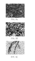
- FIGS. 3A-3C are images of titanium dioxides of different forms produced according to present invention.
- FIGS. 4A-4C are images of surfaces of different film layers of a photoelectrode according to the present invention.
- FIG. 5 shows an image of a cross section of the photoelectrode according to the present invention.
- a dye-sensitized solar cell includes a negative electrode 1 , a positive electrode 2 , a photoelectrode 3 , and an electrolyte 4 .
- the photoelectrode 3 is located between the negative electrode 1 and the positive electrode 2 .
- the electrolyte 4 is located between the photoelectrode 3 and the positive electrode 2 .
- the negative electrode 1 can be a glass substrate, a flexible substrate, or a thin film substrate coated with a transparent conductive film.
- the negative electrode 1 is a thin film substrate coated with fluorine-doped tin oxide (FTO). Desired replacement can be made by one skilled in the art. Since this is not the main feature of the present invention, detailed description is not set forth to avoid redundancy.
- FTO fluorine-doped tin oxide
- the positive electrode 2 is mounted opposite to the negative electrode 1 .
- the positive electrode 2 can be a glass substrate, a flexible substrate, or a thin film substrate coated with a transparent conductive film, allowing transfer of electrons. Desired replacement can be made by one skilled in the art. Since this is not the main feature of the present invention, detailed description is not set forth to avoid redundancy.
- a catalyst layer 21 is bonded to a surface of the positive electrode 2 facing the negative electrode 1 and located between the positive electrode 2 and the electrolyte 4 to accelerate oxidation/reduction reaction.
- the catalyst layer 21 is preferably a film formed by stacking nanoparticles of platinum.
- the photoelectrode 3 can be made of a semiconductive material to absorb a dye D.
- the dye D is a composition of ruthenium complex.
- the photoelectrode 3 is formed by three different types of titanium dioxides and includes a dense layer 31 , a scattering layer 32 , and a carrier transport layer 33 that are stacked one upon another. The stacking relation or sequence between the dense layer 31 , the scattering layer 32 , and the carrier transport layer 33 is not limited.
- the dense layer 31 , the scattering layer 32 , and the carrier transport layer 33 can be stacked in sequence, with the scattering layer 32 located between the dense layer 31 and the carrier transport layer 33 , with the dense layer 31 located on the negative electrode 1 , as shown in FIG. 1 .
- the dense layer 31 , the carrier transport layer 33 , and the scattering layer 32 can be stacked in sequence, with the carrier transport layer 33 located between the dense layer 31 and the scattering layer 32 , with the dense layer 31 located on the negative electrode 1 , as shown in FIG. 2 .
- the photoelectric conversion efficiency of the dye-sensitized solar cell according to the present invention can be improved through the differences of forms between these layers and can be proved by the following description and experiments.
- the dense layer 31 is formed by titanium dioxide nanoparticles having a diameter of 15-20 nm. Due to compact arrangement among the titanium dioxide nanoparticles, only tiny gaps exist in the dense layer 31 , preventing generation of dark current.
- the dense layer 31 can have a thickness of 3-6 ⁇ m.
- the scattering layer 32 is formed by titanium dioxide nanospheres having a diameter of 200-500 nm. The titanium dioxide nanospheres have larger contact areas with the light source. Thus, the scattering layer 32 can fully absorb the sunlight and produce a light scattering effect.
- the scattering layer 32 can have a thickness of 8-11 ⁇ m.
- the carrier transport layer 33 is formed by titanium dioxide nanotubes having a length of 300-800 nm. The titanium dioxide nanotubes intersect with one another and form numerous tiny slits. The one-dimension pattern presented by the tiny slits and the shapes of the titanium dioxide nanotubes not only increases the infiltrability of the carrier transport layer 33 but assists in transport electrons.
- the carrier transport layer 33 can have
- the electrolyte 4 is a liquid electrolyte or gel electrolyte, which can be appreciated by one skilled in the art.
- the electrolyte 4 can include iodine ions and iodine complex ions. Since this is not the main feature of the present invention, detailed description is not set forth to avoid redundancy.
- the scattering layer 32 of the photoelectrode 3 provides a better light scattering effect of the light source and forces the dye D to fully absorb the energy of photons, turning the molecules of the dye D from the ground state into the excited state. Furthermore, when the dye D in the excited state transfers electrons, the carrier transport layer 33 of the photoelectrode 3 speeds up the transport of electrons to rapidly inject the electrons into the conduction band of the photoelectrode 3 such that the photoelectrode 3 is fully charged.
- the dense layer 31 of the photoelectrode 3 avoids the electron from flowing into the electrolyte 4 in the reverse direction, avoiding generation of dark current.
- the electrons pass through an external loop and are guided to the positive electrode 2 , forming a cycle and generating photocurrent.
- the dye D returns to the ground state after the lost electrons are compensated by the electrolyte 4 .
- Powders of titanium dioxide nanoparticles having a diameter of 15-20 nm, powders of titanium dioxide nanospheres having a diameter of 200-500 nm, and powders of titanium dioxide nanotubes having a length of 300-800 nm were respectively mixed in a solvent.
- a binder was added into the solvent to make the powders of titanium dioxide nanoparticles, the powders of titanium dioxide nanospheres, and the powders of titanium dioxide nanotubes respectively and homogenously mix with the solvent, forming a particle-shaped paste, a ball-shaped paste, and a tube-shaped paste, respectively.
- the particle-shaped paste, the sphere-shaped paste, and the tube-shaped paste respectively formed a dense layer, a scattering layer, and a carrier transport layer.
- the dense layer, the scattering layer, and the carrier transport layer were stacked on a substrate to form a photoelectrode.
- the stacking relation between the dense layer, the scattering layer, and the carrier transport layer can be changed according to the situations.
- the particle-shaped paste, the tube-shaped paste, and the sphere-shaped paste are coated on the substrate in sequence and then calcined and baked to form the dense layer, the carrier transport layer, and the scattering layer on the substrate in sequence, improving the photoelectric transfer efficiency.
- the binder can be polyethylene glycol (PEG) or the like.
- PEG polyethylene glycol
- the binder can reduce aggregation among the powders, increasing the film-forming property and adhesion of the paste.
- the paste forms a porous film structure after sintering, which is advantageous to absorption of the dye.
- powders of titanium dioxide nanoparticles having a diameter of 15-20 nm (hereinafter referred to as “NP20”, see FIG. 3A ), powders of titanium dioxide nanospheres having a diameter of 200-500 nm (hereinafter referred to as “NS”, see FIG. 3B ), and the powders of titanium dioxide nanotubes having a length of 300-800 nm (hereinafter referred to as “NT”, see FIG. 3C ) were produced by the hydrothermal process.
- About 1.3 g of NP20, 1.3 g of NS, and 1.3 g of NT were respectively added into secondary water of about 8.7 ml and stirred for 30 minutes.
- a doctor blade method was used in the procedures in the following examples to form the photoelectrodes according to the present invention under a working area of 0.25 cm 2 .
- the particle-shaped paste (NP20) was applied to a substrate coated with fluorine-doped tin oxide and dried at 80° C. for 30 minutes. The substrate was then placed in a calciner and heated to 450° C. and remained at this temperature for 30 minutes, with the temperature increasing rate of the calciner controlled to be 10° C./min. After cooling to the room temperature, a layer of NP20 (the dense layer 31 , FIG. 4A shows its surface pattern) having a thickness of about 4.8 ⁇ m was formed on a surface of the substrate. The sphere-shaped plating liquid (NS) was coated on the layer of NP20 and dried at the room temperature.
- a layer of NP (the scattering layer 32 , FIG. 4B shows its surface pattern) having a thickness of about 6.0 ⁇ m was formed on a face of the layer of NP20.
- the tube-shaped plating liquid (NT) was coated on the layer of NS for carrying out the above procedures.
- FIG. 5 shows its surface pattern) having a thickness of about 9.6 ⁇ m was formed on a face of the layer of NS.
- a photoelectrode formed by NP20/NS/NT shown in FIG. 5 was stacked on the substrate and had an overall thickness of about 20.4 ⁇ m.
- example 1 The production procedures of example 1 were carried out, with the stacking relation changed to produce a photoelectrode formed by NP20/NT/NS on the substrate. Detailed description is not set forth to avoid redundancy
- example 1 The production procedures of example 1 were carried out, with the stacking relation changed to produce a photoelectrode formed by NT/NP20/NS on the substrate. Detailed description is not set forth to avoid redundancy.
- NP20/NS/NT In addition to the above three examples of NP20/NS/NT, NP20/NT/NS, and NT/NP20/NS, two-layer photoelectrodes formed by NP20/NS and NP20/NT and a photoelectrode formed by a single layer of NP20 were made and served as comparative examples for comparison with examples 1, 2, and 3.
- hydrothermal process for producing different types of titanium dioxide can be varied by one skilled in the art to produce powders of titanium dioxide nanoparticles having a diameter of 15-20 nm, powders of titanium dioxide nanospheres having a diameter of 200-500 nm, and powders of titanium dioxide nanotubes having a length of 300-800 nm.
- An example of the hydrothermal process is set forth below without any limitative purposes.
- the above nanoparticles of NP20 and solid sodium hydroxide (having a weight ratio about 1:12) were added into deionized water (30 ml/g) and stirred continuously. Heating circumfluence was carried out at 110° C. for 48 hours. After cooling, acid washing was carried out until the aqueous solution became acidic and a portion of solid powders deposited. After continuous immersion and cleaned with deionized water to make the aqueous solution become neutral, cooling and baking were conducted. High temperature calcination was carried out at 450° C. for 30 minutes to obtain crystal type titanium dioxide nanotubes of anatase, with the titanium dioxide nanotubes having a length about 400-800 nm and having a single-layer tube wall (see the NT nanotubes shown in FIG. 3C ), with the titanium dioxide nanotubes having an outer diameter of about 16.0 nm and an inner diameter of about 6.0 nm.
- dye-sensitized solar cells made from the photoelectrodes of the above example possess different photoelectric conversion efficiencies
- dye-sensitized solar cells having different photoelectrodes were produced according to the methods known by persons skilled in the art. These methods for producing dye-sensitized solar cells can be appreciated by one having ordinary skill in the art, and detailed description of which is not set forth to avoid redundancy.
- the dye-sensitized solar cells made from the above NP20, NP20/NS, NP20/NT, NP20NS/NT, NP20/NT/NS, and NTNP20/NS photoelectrodes were radiated by a solar simulator, and a current-voltage generator was used to measure and digitize the current-voltage of each photoelectrode, wherein the light intensity of the solar simulator was 100 mW/cm 2 (i.e., a sun).
- V oc is the open-circuit voltage
- J sc is the current density
- F.F. is the filling factor
- ⁇ is the photoelectric conversion efficiency
- the photoelectric conversion efficiency of the dye-sensitized solar cell including NP20 photoelectrode is only 4.58%.
- the photoelectric conversion efficiency of the dye-sensitized solar cell including NP20/NS or NP20/NT photoelectrode is only 5.06%-5.96%.
- the photoelectric conversion efficiencies of the dye-sensitized solar cells including NP20/NS/NT, NP20/NT/NS, and NT/NP20/NS photoelectrodes are higher than 6.57%.
- the photoelectric conversion efficiency of the dye-sensitized solar cell using NP20/NS/NT photoelectrode is 7.83%.
- the photoelectric conversion efficiency of the dye-sensitized solar cell using NP20/NT/NS photoelectrode is 8.53%.
- the photoelectric conversion efficiency of the dye-sensitized solar cell according to the present invention increases the power source utility rate, increases the carrier mobility, and inhibits generation of dark current, such that the photoelectric conversion efficiency is significantly increased.
- the method for producing the photoelectrode of a dye-sensitized solar cell according to the present invention can continuously produce different types of titanium dioxide powders by the hydrothermal process for subsequent production of the photoelectrode formed by stacking three different types of titanium dioxide, not only reducing the working hours and cost but simplifying the procedures to achieve continuous mass production.
- the film-forming property and adhesion of the paste are enhanced to increase the fitness between the films, and the dye can be fully absorbed by the porous films, maintaining the formation quality of the photoelectrode and increasing the photoelectric conversion efficiency.
Landscapes
- Engineering & Computer Science (AREA)
- Power Engineering (AREA)
- Microelectronics & Electronic Packaging (AREA)
- Computer Hardware Design (AREA)
- Physics & Mathematics (AREA)
- Condensed Matter Physics & Semiconductors (AREA)
- Electromagnetism (AREA)
- General Physics & Mathematics (AREA)
- Manufacturing & Machinery (AREA)
- Life Sciences & Earth Sciences (AREA)
- Sustainable Development (AREA)
- Sustainable Energy (AREA)
- Hybrid Cells (AREA)
- Photovoltaic Devices (AREA)
Applications Claiming Priority (3)
| Application Number | Priority Date | Filing Date | Title |
|---|---|---|---|
| TW101131793A | 2012-08-31 | ||
| TW101131793A TWI481047B (zh) | 2012-08-31 | 2012-08-31 | 染料敏化太陽能電池、其光電極及光電極製作方法 |
| TW101131793 | 2012-08-31 |
Publications (2)
| Publication Number | Publication Date |
|---|---|
| US20140060637A1 US20140060637A1 (en) | 2014-03-06 |
| US8796545B2 true US8796545B2 (en) | 2014-08-05 |
Family
ID=50185750
Family Applications (1)
| Application Number | Title | Priority Date | Filing Date |
|---|---|---|---|
| US13/684,312 Expired - Fee Related US8796545B2 (en) | 2012-08-31 | 2012-11-23 | Dye-sensitized solar cell, its photoelectrode and producing method thereof |
Country Status (2)
| Country | Link |
|---|---|
| US (1) | US8796545B2 (zh) |
| TW (1) | TWI481047B (zh) |
Families Citing this family (3)
| Publication number | Priority date | Publication date | Assignee | Title |
|---|---|---|---|---|
| US20160225534A1 (en) * | 2010-12-16 | 2016-08-04 | National Yunlin University Of Science And Technology | Composite dye-sensitized solar cell |
| US20130327401A1 (en) * | 2010-12-16 | 2013-12-12 | National Yunlin University Of Science And Technology | Composite dye-sensitized solar cell |
| TWI722569B (zh) * | 2019-09-16 | 2021-03-21 | 國立成功大學 | 雙面受光型染料敏化太陽能電池 |
Citations (5)
| Publication number | Priority date | Publication date | Assignee | Title |
|---|---|---|---|---|
| US20070209696A1 (en) * | 2004-04-23 | 2007-09-13 | Sony Deutschland Gmbh | Method of Producing a Porous Semiconductor Film on a Substrate |
| US20100300516A1 (en) * | 2005-06-14 | 2010-12-02 | Seiko Epson Corporation | Multilayer structure, photoelectric element and electronic apparatus |
| US20110030770A1 (en) | 2009-08-04 | 2011-02-10 | Molecular Imprints, Inc. | Nanostructured organic solar cells |
| TWM403755U (en) | 2010-11-05 | 2011-05-11 | Ho Chang | Multilayer nano-tio2 photoelectrode thin films for dye-sensitized solar cells |
| US20130074913A1 (en) * | 2011-09-26 | 2013-03-28 | The Hong Kong Polytechnic University | Bilayer dye sensitized solar cell and fabrication method thereof |
Family Cites Families (5)
| Publication number | Priority date | Publication date | Assignee | Title |
|---|---|---|---|---|
| JP4710251B2 (ja) * | 2004-05-28 | 2011-06-29 | 凸版印刷株式会社 | 金属酸化物膜の製造方法 |
| TW200823149A (en) * | 2006-11-20 | 2008-06-01 | Iner Aec Executive Yuan | The manufacturing method of titanium dioxide slurry and the application thereof |
| TWI419392B (zh) * | 2010-07-30 | 2013-12-11 | Ind Tech Res Inst | 多層結構奈米二氧化鈦光電極及其製造方法 |
| TWM436222U (en) * | 2011-12-02 | 2012-08-21 | Univ Hsiuping Sci & Tech | Dye sensitized solar working electrode and improved battery structure applying the same |
| CN102592838A (zh) * | 2012-03-09 | 2012-07-18 | 北京大学 | 染料敏化太阳能电池的叠层纳米半导体薄膜电极 |
-
2012
- 2012-08-31 TW TW101131793A patent/TWI481047B/zh not_active IP Right Cessation
- 2012-11-23 US US13/684,312 patent/US8796545B2/en not_active Expired - Fee Related
Patent Citations (5)
| Publication number | Priority date | Publication date | Assignee | Title |
|---|---|---|---|---|
| US20070209696A1 (en) * | 2004-04-23 | 2007-09-13 | Sony Deutschland Gmbh | Method of Producing a Porous Semiconductor Film on a Substrate |
| US20100300516A1 (en) * | 2005-06-14 | 2010-12-02 | Seiko Epson Corporation | Multilayer structure, photoelectric element and electronic apparatus |
| US20110030770A1 (en) | 2009-08-04 | 2011-02-10 | Molecular Imprints, Inc. | Nanostructured organic solar cells |
| TWM403755U (en) | 2010-11-05 | 2011-05-11 | Ho Chang | Multilayer nano-tio2 photoelectrode thin films for dye-sensitized solar cells |
| US20130074913A1 (en) * | 2011-09-26 | 2013-03-28 | The Hong Kong Polytechnic University | Bilayer dye sensitized solar cell and fabrication method thereof |
Also Published As
| Publication number | Publication date |
|---|---|
| TWI481047B (zh) | 2015-04-11 |
| TW201409725A (zh) | 2014-03-01 |
| US20140060637A1 (en) | 2014-03-06 |
Similar Documents
| Publication | Publication Date | Title |
|---|---|---|
| Lin et al. | Photoactive p-type PbS as a counter electrode for quantum dot-sensitized solar cells | |
| Guan et al. | Enhanced photoelectrochemical performances of ZnS-Bi2S3/TiO2/WO3 composite film for photocathodic protection | |
| Mustafa et al. | Review on the effect of compact layers and light scattering layers on the enhancement of dye-sensitized solar cells | |
| JP5389372B2 (ja) | 中空球状の金属酸化物ナノ粒子を含む色素増感太陽電池用の光電極及びその製造方法 | |
| Bakhshayesh et al. | Improved efficiency of dye-sensitized solar cells aided by corn-like TiO2 nanowires as the light scattering layer | |
| Liu et al. | Anatase TiO2 hollow spheres with small dimension fabricated via a simple preparation method for dye-sensitized solar cells with an ionic liquid electrolyte | |
| Qadir et al. | Composite multi-functional over layer: A novel design to improve the photovoltaic performance of DSSC | |
| Jalali et al. | Enhanced dye loading-light harvesting TiO2 photoanode with screen printed nanorod-nanoparticles assembly for highly efficient solar cell | |
| Chang et al. | Broadband light confinement using a hierarchically structured TiO 2 multi-layer for dye-sensitized solar cells | |
| Cui et al. | A comparative study on the quantum-dot-sensitized, dye-sensitized and co-sensitized solar cells based on hollow spheres embedded porous TiO2 photoanodes | |
| Xu et al. | Hierarchical submicroflowers assembled from ultrathin anatase TiO2 nanosheets as light scattering centers in TiO2 photoanodes for dye-sensitized solar cells | |
| Baraton | Nano-TiO2 for dye-sensitized solar cells | |
| Chou et al. | Bilayer structure of TiO 2/TiO 2-graphene for optimizing working electrode applied in dye sensitized solar cells | |
| US8796545B2 (en) | Dye-sensitized solar cell, its photoelectrode and producing method thereof | |
| Mao et al. | Nanowire-based zinc-doped tin oxide microtubes for enhanced solar energy utilization efficiency | |
| Yang et al. | Light-scattering photoanodes from double-layered mesoporous TiO2 nanoparticles/SiO2 nanospheres for dye-sensitized solar cells | |
| Mutashar et al. | Enhancing of dye-sensitized solar cells efficiency using graphene-MWCNT nanocomposite as photoanode | |
| Huo et al. | Fabrication a thin nickel oxide layer on photoanodes for control of charge recombination in dye-sensitized solar cells | |
| Chen et al. | Characterization of dye-sensitized solar cells based on various CaCO3-doped ZnO photoanodes prepared using wet powder mixing and grinding | |
| Huang et al. | Bilayer TiO2 photoanode consisting of microspheres and pyramids with reinforced interface connection and light utilization for dye-sensitized solar cells | |
| Pari et al. | Recent advances in SnO2 based photo anode materials for third generation photovoltaics | |
| Liu et al. | Efficiency enhancement of DSSC by alternating TiO2 active layer | |
| Hejazi et al. | The effect of functionally graded porous nano structure TiO2 photoanode on efficiency of dye sensitized solar cells | |
| Senadeera et al. | A five-fold efficiency enhancement in dye sensitized solar cells fabricated with AlCl 3 treated, SnO 2 nanoparticle/nanofibre/nanoparticle triple layered photoanode | |
| Qu et al. | Upconverting TiO2 spheres with light scattering effect for enhanced quantum dot-sensitized solar cells |
Legal Events
| Date | Code | Title | Description |
|---|---|---|---|
| AS | Assignment |
Owner name: I-SHOU UNIVERSITY, TAIWAN Free format text: ASSIGNMENT OF ASSIGNORS INTEREST;ASSIGNORS:HUNG, TIEN-TSAN;BAI, JUN-YU;REEL/FRAME:029343/0451 Effective date: 20120917 |
|
| FEPP | Fee payment procedure |
Free format text: MAINTENANCE FEE REMINDER MAILED (ORIGINAL EVENT CODE: REM.) |
|
| LAPS | Lapse for failure to pay maintenance fees |
Free format text: PATENT EXPIRED FOR FAILURE TO PAY MAINTENANCE FEES (ORIGINAL EVENT CODE: EXP.); ENTITY STATUS OF PATENT OWNER: SMALL ENTITY |
|
| STCH | Information on status: patent discontinuation |
Free format text: PATENT EXPIRED DUE TO NONPAYMENT OF MAINTENANCE FEES UNDER 37 CFR 1.362 |
|
| FP | Lapsed due to failure to pay maintenance fee |
Effective date: 20180805 |