US8785224B2 - Organic light emitting display apparatus and method of manufacturing the same - Google Patents
Organic light emitting display apparatus and method of manufacturing the same Download PDFInfo
- Publication number
- US8785224B2 US8785224B2 US13/029,617 US201113029617A US8785224B2 US 8785224 B2 US8785224 B2 US 8785224B2 US 201113029617 A US201113029617 A US 201113029617A US 8785224 B2 US8785224 B2 US 8785224B2
- Authority
- US
- United States
- Prior art keywords
- electrode
- layer
- electrodes
- conductive layer
- light emitting
- Prior art date
- Legal status (The legal status is an assumption and is not a legal conclusion. Google has not performed a legal analysis and makes no representation as to the accuracy of the status listed.)
- Active, expires
Links
Images


Classifications
-
- H—ELECTRICITY
- H10—SEMICONDUCTOR DEVICES; ELECTRIC SOLID-STATE DEVICES NOT OTHERWISE PROVIDED FOR
- H10K—ORGANIC ELECTRIC SOLID-STATE DEVICES
- H10K59/00—Integrated devices, or assemblies of multiple devices, comprising at least one organic light-emitting element covered by group H10K50/00
- H10K59/80—Constructional details
- H10K59/805—Electrodes
- H10K59/8051—Anodes
- H10K59/80517—Multilayers, e.g. transparent multilayers
-
- H—ELECTRICITY
- H10—SEMICONDUCTOR DEVICES; ELECTRIC SOLID-STATE DEVICES NOT OTHERWISE PROVIDED FOR
- H10K—ORGANIC ELECTRIC SOLID-STATE DEVICES
- H10K50/00—Organic light-emitting devices
- H10K50/80—Constructional details
- H10K50/805—Electrodes
- H10K50/81—Anodes
- H10K50/816—Multilayers, e.g. transparent multilayers
-
- H—ELECTRICITY
- H10—SEMICONDUCTOR DEVICES; ELECTRIC SOLID-STATE DEVICES NOT OTHERWISE PROVIDED FOR
- H10K—ORGANIC ELECTRIC SOLID-STATE DEVICES
- H10K59/00—Integrated devices, or assemblies of multiple devices, comprising at least one organic light-emitting element covered by group H10K50/00
- H10K59/10—OLED displays
- H10K59/12—Active-matrix OLED [AMOLED] displays
- H10K59/122—Pixel-defining structures or layers, e.g. banks
-
- H—ELECTRICITY
- H10—SEMICONDUCTOR DEVICES; ELECTRIC SOLID-STATE DEVICES NOT OTHERWISE PROVIDED FOR
- H10K—ORGANIC ELECTRIC SOLID-STATE DEVICES
- H10K59/00—Integrated devices, or assemblies of multiple devices, comprising at least one organic light-emitting element covered by group H10K50/00
- H10K59/80—Constructional details
- H10K59/805—Electrodes
- H10K59/8051—Anodes
- H10K59/80515—Anodes characterised by their shape
-
- H—ELECTRICITY
- H10—SEMICONDUCTOR DEVICES; ELECTRIC SOLID-STATE DEVICES NOT OTHERWISE PROVIDED FOR
- H10K—ORGANIC ELECTRIC SOLID-STATE DEVICES
- H10K71/00—Manufacture or treatment specially adapted for the organic devices covered by this subclass
-
- H—ELECTRICITY
- H10—SEMICONDUCTOR DEVICES; ELECTRIC SOLID-STATE DEVICES NOT OTHERWISE PROVIDED FOR
- H10K—ORGANIC ELECTRIC SOLID-STATE DEVICES
- H10K71/00—Manufacture or treatment specially adapted for the organic devices covered by this subclass
- H10K71/40—Thermal treatment, e.g. annealing in the presence of a solvent vapour
-
- H—ELECTRICITY
- H10—SEMICONDUCTOR DEVICES; ELECTRIC SOLID-STATE DEVICES NOT OTHERWISE PROVIDED FOR
- H10K—ORGANIC ELECTRIC SOLID-STATE DEVICES
- H10K71/00—Manufacture or treatment specially adapted for the organic devices covered by this subclass
- H10K71/60—Forming conductive regions or layers, e.g. electrodes
-
- H—ELECTRICITY
- H10—SEMICONDUCTOR DEVICES; ELECTRIC SOLID-STATE DEVICES NOT OTHERWISE PROVIDED FOR
- H10K—ORGANIC ELECTRIC SOLID-STATE DEVICES
- H10K71/00—Manufacture or treatment specially adapted for the organic devices covered by this subclass
- H10K71/621—Providing a shape to conductive layers, e.g. patterning or selective deposition
-
- H—ELECTRICITY
- H10—SEMICONDUCTOR DEVICES; ELECTRIC SOLID-STATE DEVICES NOT OTHERWISE PROVIDED FOR
- H10K—ORGANIC ELECTRIC SOLID-STATE DEVICES
- H10K2102/00—Constructional details relating to the organic devices covered by this subclass
- H10K2102/10—Transparent electrodes, e.g. using graphene
- H10K2102/101—Transparent electrodes, e.g. using graphene comprising transparent conductive oxides [TCO]
Definitions
- aspects of the present invention relate to an organic light emitting display apparatus and a method of manufacturing the same, and more particularly, to an organic light emitting display apparatus which improves an image quality and a method of manufacturing the same.
- Organic or inorganic light emitting display apparatuses are types of the thin flat display apparatuses. They are self-emissive display apparatuses that have wide viewing angles, excellent contrast, and rapid response speed. Thus, the organic or inorganic light emitting display apparatuses have been highlighted as next generation display apparatuses. Also, organic light emitting display apparatuses including an emission layer formed of an organic material have excellent properties in terms of brightness, driving voltages, and response speed compared with those of inorganic light emitting display apparatuses, and may display various colors.
- aspects of the present invention provide an organic light emitting display apparatus which may easily improve an image quality property and a method of manufacturing the same.
- an organic light emitting display apparatus including: a first electrode formed on a substrate; an intermediate layer disposed on the first electrode, the intermediate layer having an organic emission layer; and a second electrode formed on the intermediate layer, wherein the first electrode includes an etching unit facing the intermediate layer.
- the apparatus may further include a pixel defining layer disposed on the first electrode and exposing a predetermined area of the first electrode, wherein the etching unit is formed on the exposed area of the first electrode.
- the first electrode may include silver (Ag).
- an area of the first electrode having the etching unit may be crystallized.
- an area of the first electrode having the etching unit may include crystallized ITO.
- the first electrode may include a first conductive layer; a second conductive layer; and a third conductive layer, wherein the first electrode is formed in a stacked structure stacking the first conductive layer, the second conductive layer and the third conductive layer, wherein the first conductive layer and the third conductive layer include ITO and wherein the second conductive layer includes silver (Ag).
- the etching unit may be formed on the third conductive layer.
- the method may further include: forming a pixel defining layer on the first electrode so as to expose a predetermined area of the first electrode after forming the first electrode and before forming the intermediate layer; and forming the etching unit by etching the exposed area of the first electrode.
- the etching unit may be formed by wet etching the first electrode.
- the etching unit may be formed by an oxalic acid.
- the first electrode may include silver (Ag).
- the method may further include crystallizing the surface of the first electrode before forming the etching unit on the first electrode.
- a surface of the first electrode may include ITO and wherein the crystallizing of the first electrode comprises crystallizing ITO.
- the crystallizing the surface of the first electrode may be performed by a heat treatment.
- the first electrode may include a first conductive layer; a second conductive layer; and a third conductive layer, wherein the first electrode is formed in a stacked structure stacking the first conductive layer, the second conductive layer, and the third conductive layer, wherein the first conductive layer and the third conductive layer include ITO and wherein the second conductive layer includes silver (Ag).
- the etching unit may be formed on the third conductive layer.
- FIG. 1 is a cross-sectional diagram of an organic light emitting display apparatus according to an embodiment of the present invention
- FIGS. 2A through 2F are cross-sectional diagrams sequentially illustrating a method of manufacturing the organic light emitting display apparatus of FIG. 1 according to an embodiment of the present invention
- FIG. 3 is a cross-sectional diagram of an organic light emitting display apparatus according to another embodiment of the present invention.
- FIGS. 4A through 4F are cross-sectional diagrams sequentially illustrating a method of manufacturing an organic light emitting display apparatus according to another embodiment of the present invention.
- FIG. 1 is a cross-sectional diagram of an organic light emitting display apparatus 100 according to an embodiment of the present invention.
- first electrodes 110 are formed on a substrate 101 and a pixel defining layer 115 is formed on the first electrodes 110 .
- Intermediate layers 120 are formed on portions exposed by the pixel defining layer 115 and a second electrode 130 is formed on the intermediate layers 120 .
- Etching units 110 a are formed on the surfaces of the first electrodes 110 facing the intermediate layers 120 . More specifically, the etching units 110 a are formed on the surfaces of the first electrodes 110 exposed by the pixel defining layer 115 . The etching units 110 a are formed on the first electrodes 110 so as to easily remove impurities remaining on the surfaces of the first electrodes 110 .
- the first electrodes 110 include silver (Ag). In this case, the etching units 110 a are formed so that silver (Ag) particles are not remaining on the surfaces of the first electrodes 110 .
- the etching units 110 a are formed on the surfaces of the first electrodes 110 that are exposed and not covered by the pixel defining layer 115 in order to prevent the sides and edges of the first electrodes 110 from being damaged.
- FIGS. 2A through 2F are cross-sectional diagrams sequentially illustrating a method of manufacturing the organic light emitting display apparatus 100 according to an embodiment of the present invention.
- the substrate 101 may be formed of a metal.
- the substrate 101 may include at least one selected from the group consisting of carbon (c), iron (Fe), chromium (Cr), manganese (Mn), nickel (Ni), titanium (Ti), molybdenum (Mo), stainless steel (SUS), an Invar alloy, an Inconel alloy, and a Kovar alloy.
- the substrate 101 may be formed of a metal foil or other suitable materials.
- a buffer layer (not illustrated) may be formed on the substrate 101 in order to form a smooth surface on the substrate 101 and to prevent impurity elements from penetrating the substrate 101 .
- the buffer layer may be formed of SiO 2 , SiNx, or other suitable materials.
- the first electrodes 110 include various materials, such as silver (Ag). When the first electrodes 110 include silver (Ag), visible rays radiating towards the first electrodes 110 from an intermediate layer 120 may be reflected toward the second electrode 130 . Surfaces far from the substrate 101 from among the surfaces of the first electrode 110 facing the intermediate layer 120 , may include ITO. However, aspects of the present invention are not limited thereto, and the surfaces of the first electrode 110 facing the intermediate layer 120 may include other suitable materials.
- the pixel defining layer 115 is formed on the first electrodes 110 .
- the pixel defining layer 115 is formed to expose predetermined areas of the first electrodes 110 .
- the pixel defining layer 115 may be formed of various insulating materials, such as organic materials, inorganic materials or other suitable materials.
- the etching units 110 a are formed on the first electrodes 110 .
- a process of crystallizing the surfaces of the first electrodes 110 is performed before the etching units 110 a are formed.
- the process of crystallizing the surfaces of the first electrodes 110 is performed by heat treatment or other suitable processes.
- the surfaces of the first electrodes 110 include ITO, such a heat treatment is performed at a temperature that crystallizes the ITO.
- the etching units 110 a are formed on the surfaces of the first electrodes 110 exposed by the pixel defining layer 115 .
- the etching units 110 a are formed by using an oxalic acid C 2 H 2 O 4 .
- the intermediate layers 120 are formed on the first electrodes 110 .
- the intermediate layers 120 each include an organic emission layer that emits visible rays and may be each formed of various materials.
- the second electrode 130 is formed on the intermediate layers 120 , and FIG. 2F illustrates the organic light emitting display apparatus 100 .
- the second electrode 130 is formed to cover all sub pixels. However, aspects of the present invention are not limited thereto, and the second electrode 130 may not cover all of the sub pixels.
- the second electrode 130 is formed by depositing a metal having a small work function, that is, silver (Ag), manganese (Mg), aluminum (Al), platinum (Pt), palladium (Pd), gold (Au), nickel (Ni), neodymium (Nd), iridium (Ir), chromium (Cr), lithium (Li), calcium (Ca), or a compound thereof and then depositing a transparent conductive material such as TO, IZO, ZnO, or In2O3 on the deposited metal.
- a transparent conductive material such as TO, IZO, ZnO, or In2O3
- the first electrodes 110 are formed and then the etching units 110 a , which are formed so that residual patterns such as silver (Ag) remaining on the surfaces of the first electrodes 110 are easily removable. Accordingly, defects such as a dark spot are prevented and an image quality of the organic light emitting display apparatus 100 may be improved.
- the pixel defining layer 115 is formed and then the etching units 110 a are formed so that the sides of the first electrode 110 are prevented from being damaged. Also, the surfaces of the first electrodes 110 are crystallized and are prevented from being excessively etched. Thus, electrical characteristics of the first electrodes 110 are not affected and thereby, an image quality property of the organic light emitting display apparatus 100 may be improved.
- An oxalic acid used to form the etching units 110 a completely removes silver (Ag) remaining on the first electrode 110 and has an etching capability to appropriately etch crystallized ITO so that the etching units 110 a are formed in a desired form. Also, the etching units 110 a are formed on the first electrodes 110 and thus the intermediate layers 120 are formed on the etching units 110 a so that adhesive strength between the intermediate layers 120 and the first electrodes 110 may be improved.
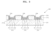
- FIG. 3 is a cross-sectional diagram of an organic light emitting display apparatus 200 according to another embodiment of the present invention.
- first electrodes 210 are formed on a substrate 201 and a pixel defining layer 215 is formed on the first electrodes 210 .
- Intermediate layers 220 are formed on portions exposed by the pixel defining layer 215 and a second electrode 230 is formed on the intermediate layers 220 .
- the first electrodes 210 each include a first conductive layer 211 , a second conductive layer 212 , and a third conductive layer 213 .
- the first conductive layer 211 and the third conductive layer 213 include ITO and the second conductive layer 212 may include silver (Ag).
- Etching units 210 a are formed on the surfaces of the first electrodes 210 facing the intermediate layers 220 . More specifically, the etching units 210 a are formed on the surfaces of the third conductive layer 213 exposed by the pixel defining layer 215 in the first electrodes 210 . The etching units 210 a are each formed on the third conductive layer 213 and thus impurities remaining on the surface of the third conductive layer 213 are easily removed. The etching units 210 a are formed on the surfaces of the first electrodes 210 that are exposed and not covered by the pixel defining layer 215 in order to prevent the sides and edges of the first electrodes 210 being damaged.
- a sealing member (not illustrated) is disposed on the second electrode 230 in order to face one surface of the substrate 201 .
- the sealing member (not illustrated) is formed to protect an organic light emission layer from external moisture and oxygen and is formed of a transparent material. Accordingly, the sealing member is formed of glass, plastic, or a stacked structure of an organic material and an inorganic layer. However, aspects of the present invention are not limited thereto, and the sealing member may be formed of other suitable materials, and in other suitable structures.
- FIGS. 4A through 4F are cross-sectional diagrams sequentially illustrating a method of manufacturing the organic light emitting display apparatus 200 according to another embodiment of the present invention.
- the substrate 201 is prepared, wherein a material forming the substrate 201 is the same as the material described in the previous embodiment and thus a detailed description thereof is omitted.
- a buffer layer (not illustrated) may be formed on the substrate 201 .
- the first electrodes 210 are formed on the substrate 201 .
- the first electrodes 210 are patterned in a predetermined form.
- the first electrodes 210 are patterned in a stripe form.
- the first electrodes 210 are patterned to correspond to each sub pixel.
- aspects of the present invention are not limited thereto, and the first electrodes 210 may be patterned in other suitable patterns.
- the first electrodes 210 each include the first conductive layer 211 , the second conductive layer 212 , and the third conductive layer 213 .
- the first conductive layer 211 includes ITO and accordingly, adhesive strength between the first electrodes 210 and the substrate 201 may be improved. When another insulating layer is interposed between the substrate 201 and the first electrodes 210 , adhesive strength between the insulating layer and the first electrodes 210 also may be improved.
- the second conductive layer 212 formed on the first conductive layer 211 includes silver (Ag). The second conductive layer 212 allows visible rays radiating towards the first electrodes 210 from an intermediate layer 220 to be reflected toward the second electrode 230 .
- the third conductive layer 213 formed on the second conductive layer 212 includes ITO.
- the pixel defining layer 215 is formed on the first electrodes 210 .
- the pixel defining layer 215 is formed to expose predetermined areas of the first electrodes 210 .
- the etching units 210 a are formed on the first electrodes 210 .
- the surfaces of the first electrodes 210 are crystallized. That is, the third conductive layer 213 of the first electrode 210 is crystallized.
- a process of crystallizing the surfaces of the first electrodes 210 is performed by heat treatment, or may be performed by other suitable processes.
- the third conductive layer 213 of the first electrode 210 includes ITO, such a heat treatment is performed at a temperature that crystallizes the ITO.
- the etching units 210 a are formed on the surfaces of the first electrodes 210 exposed by the pixel defining layer 215 . More specifically, the etching units 210 a are formed on the third conductive layer 213 of the first electrode 210 .
- the etching units 210 a are formed by using an oxalic acid C 2 H 2 O 4 .
- residual patterns may remain on the surfaces of the first electrodes 210 .
- silver (Ag) components included in the second conductive layer 212 of the first electrode 110 may remain.
- impurities such as the silver (Ag) component remaining on the first electrodes 210 is easily removable.
- the pixel defining g layer 215 prevents the sides and edges of the first electrodes 210 from being damaged by an oxalic acid.
- the third conductive layer 213 of the first electrode 210 is crystallized and is prevented from being excessively etched when the etching units 210 a are formed using the oxalic acid. Thus, electrical characteristics of the first electrodes 210 are not affected.
- the intermediate layers 220 are formed on the first electrodes 210 .
- the intermediate layers 220 each include an organic emission layer that emits visible rays and may be each formed of various materials.
- the second electrode 230 is formed on the intermediate layers 220 , thereby completing the organic light emitting display apparatus 200 , as illustrated in FIG. 4F .
- the first electrode 210 is an anode and the second electrode 230 is a cathode.
- aspects of the present invention are not limited thereto and the first electrode 210 may be a cathode and the second electrode 230 may be an anode.
- a sealing member may be disposed on the second electrode 230 in order to face one surface of the substrate 201 .
- the sealing member (not illustrated) is formed to protect an organic light emission layer from external moisture and oxygen and is formed of a transparent material. Accordingly, the sealing member is formed of glass, plastic, or a stacked structure of an organic material and an inorganic layer, or other suitable materials and in other suitable structures.
- the first electrodes 210 are formed and then the etching units 210 a are formed so that residual patterns such as silver (Ag), which is a forming material of the second conductive layer 212 , remaining on the surfaces of the first electrodes 210 are easily removable.
- the pixel defining layer 215 is formed and then the etching units 210 a are formed so that the sides of the first electrodes 210 are prevented from being damaged.
- the third conductive layer 213 of the first electrode 210 is crystallized and is prevented from being excessively etched. Thus, electrical characteristics of the first electrodes 210 are not affected and an image quality of the organic light emitting display apparatus 200 may be improved.
Landscapes
- Engineering & Computer Science (AREA)
- Manufacturing & Machinery (AREA)
- Microelectronics & Electronic Packaging (AREA)
- Physics & Mathematics (AREA)
- Optics & Photonics (AREA)
- Electroluminescent Light Sources (AREA)
Abstract
Description
Claims (11)
Applications Claiming Priority (2)
| Application Number | Priority Date | Filing Date | Title |
|---|---|---|---|
| KR10-2010-0028082 | 2010-03-29 | ||
| KR1020100028082A KR101692409B1 (en) | 2010-03-29 | 2010-03-29 | Organic light emitting display apparatus and method of manufacturing thereof |
Publications (2)
| Publication Number | Publication Date |
|---|---|
| US20110233569A1 US20110233569A1 (en) | 2011-09-29 |
| US8785224B2 true US8785224B2 (en) | 2014-07-22 |
Family
ID=44655338
Family Applications (1)
| Application Number | Title | Priority Date | Filing Date |
|---|---|---|---|
| US13/029,617 Active 2032-03-16 US8785224B2 (en) | 2010-03-29 | 2011-02-17 | Organic light emitting display apparatus and method of manufacturing the same |
Country Status (3)
| Country | Link |
|---|---|
| US (1) | US8785224B2 (en) |
| JP (1) | JP5697972B2 (en) |
| KR (1) | KR101692409B1 (en) |
Cited By (4)
| Publication number | Priority date | Publication date | Assignee | Title |
|---|---|---|---|---|
| US10611962B2 (en) | 2018-04-23 | 2020-04-07 | Samsung Display Co., Ltd. | Etchant composition and manufacturing method of metal pattern using the same |
| US10636666B1 (en) | 2018-10-11 | 2020-04-28 | Samsung Display Co., Ltd. | Etchant and method for manufacturing display device using the same |
| US11091694B2 (en) | 2018-11-14 | 2021-08-17 | Samsung Display Co., Ltd. | Etching composition, method for forming pattern and method for manufacturing a display device using the same |
| US11683975B2 (en) | 2020-04-29 | 2023-06-20 | Samsung Display Co., Ltd. | Etchant composition and method of manufacturing display apparatus by using the same |
Families Citing this family (3)
| Publication number | Priority date | Publication date | Assignee | Title |
|---|---|---|---|---|
| DE102012210484B4 (en) * | 2012-06-21 | 2017-02-02 | Osram Oled Gmbh | Method for a coherent connection of an organic optoelectronic component with a connector, connection structure for a frictional connection and optoelectronic component device |
| KR102441566B1 (en) * | 2017-08-07 | 2022-09-07 | 삼성디스플레이 주식회사 | Light emitting device and manufacturing method of light emitting device |
| KR20190058758A (en) | 2017-11-21 | 2019-05-30 | 삼성디스플레이 주식회사 | Etchant and manufacturing method of display device using the same |
Citations (11)
| Publication number | Priority date | Publication date | Assignee | Title |
|---|---|---|---|---|
| US20020070197A1 (en) * | 1999-12-28 | 2002-06-13 | Ahn You Shin | Transparent electrode made from indium-zinc-oxide and etchant for etching the same |
| KR20030044565A (en) | 2001-11-30 | 2003-06-09 | 오리온전기 주식회사 | Organic light emitting diode having black matrix and manufacturing method thereof |
| US20060118788A1 (en) * | 2004-12-07 | 2006-06-08 | Samsung Electronics Co., Ltd. | Thin film transistor array panel and method for manufacturing the same |
| US20060119258A1 (en) * | 2004-12-06 | 2006-06-08 | Semiconductor Energy Laboratory Co., Ltd. | Electronic appliance and light-emitting device |
| US20070063645A1 (en) * | 2003-05-28 | 2007-03-22 | C/O Sony Corporation | Laminated structure, display device, and display unit empolying same |
| US20070102737A1 (en) * | 2003-09-19 | 2007-05-10 | Mitsuhiro Kashiwabara | Display unit, method of manufacturing same, organic light emitting unit, and method of manufacturing same |
| KR100729042B1 (en) | 2005-11-29 | 2007-06-14 | 삼성에스디아이 주식회사 | Manufacturing method of organic light emitting display device |
| KR20070063067A (en) | 2005-12-14 | 2007-06-19 | 오리온오엘이디 주식회사 | Active organic light emitting device and manufacturing method |
| KR100783359B1 (en) | 2001-12-28 | 2007-12-07 | 엘지.필립스 엘시디 주식회사 | Organic electroluminescent device |
| US20090009064A1 (en) * | 2006-01-09 | 2009-01-08 | Jae Seung Lee | Organic Light Emitting Device Having Surface-Treated Bottom Electrode |
| US20090298377A1 (en) * | 2002-04-23 | 2009-12-03 | Semiconductor Energy Laboratory Co., Ltd. | Light emitting device and method of manufacturing the same |
Family Cites Families (9)
| Publication number | Priority date | Publication date | Assignee | Title |
|---|---|---|---|---|
| KR100600848B1 (en) * | 2001-12-26 | 2006-07-14 | 삼성에스디아이 주식회사 | Flat Panel Display and Manufacturing Method |
| JP4156431B2 (en) * | 2002-04-23 | 2008-09-24 | 株式会社半導体エネルギー研究所 | Light emitting device and manufacturing method thereof |
| JP4850393B2 (en) * | 2003-03-25 | 2012-01-11 | 株式会社半導体エネルギー研究所 | Method for manufacturing display device |
| JP2005011793A (en) * | 2003-05-29 | 2005-01-13 | Sony Corp | LAMINATED STRUCTURE MANUFACTURING METHOD, LAMINATED STRUCTURE, DISPLAY ELEMENT AND DISPLAY DEVICE |
| JP4461726B2 (en) * | 2003-07-16 | 2010-05-12 | ソニー株式会社 | ORGANIC LIGHT EMITTING ELEMENT, ITS MANUFACTURING METHOD, AND DISPLAY DEVICE |
| JP4439260B2 (en) * | 2003-12-26 | 2010-03-24 | 三洋電機株式会社 | Manufacturing method of display device |
| JP2006164961A (en) * | 2004-11-09 | 2006-06-22 | Ulvac Seimaku Kk | Method for producing laminated transparent electrode layer and laminated body for forming laminated transparent electrode used in this method |
| JP2006277989A (en) * | 2005-03-28 | 2006-10-12 | Mitsubishi Electric Corp | Manufacturing method of display device |
| KR100787461B1 (en) * | 2006-11-10 | 2007-12-26 | 삼성에스디아이 주식회사 | Organic light emitting display device employing a multilayer anode |
-
2010
- 2010-03-29 KR KR1020100028082A patent/KR101692409B1/en active Active
- 2010-12-24 JP JP2010288081A patent/JP5697972B2/en active Active
-
2011
- 2011-02-17 US US13/029,617 patent/US8785224B2/en active Active
Patent Citations (11)
| Publication number | Priority date | Publication date | Assignee | Title |
|---|---|---|---|---|
| US20020070197A1 (en) * | 1999-12-28 | 2002-06-13 | Ahn You Shin | Transparent electrode made from indium-zinc-oxide and etchant for etching the same |
| KR20030044565A (en) | 2001-11-30 | 2003-06-09 | 오리온전기 주식회사 | Organic light emitting diode having black matrix and manufacturing method thereof |
| KR100783359B1 (en) | 2001-12-28 | 2007-12-07 | 엘지.필립스 엘시디 주식회사 | Organic electroluminescent device |
| US20090298377A1 (en) * | 2002-04-23 | 2009-12-03 | Semiconductor Energy Laboratory Co., Ltd. | Light emitting device and method of manufacturing the same |
| US20070063645A1 (en) * | 2003-05-28 | 2007-03-22 | C/O Sony Corporation | Laminated structure, display device, and display unit empolying same |
| US20070102737A1 (en) * | 2003-09-19 | 2007-05-10 | Mitsuhiro Kashiwabara | Display unit, method of manufacturing same, organic light emitting unit, and method of manufacturing same |
| US20060119258A1 (en) * | 2004-12-06 | 2006-06-08 | Semiconductor Energy Laboratory Co., Ltd. | Electronic appliance and light-emitting device |
| US20060118788A1 (en) * | 2004-12-07 | 2006-06-08 | Samsung Electronics Co., Ltd. | Thin film transistor array panel and method for manufacturing the same |
| KR100729042B1 (en) | 2005-11-29 | 2007-06-14 | 삼성에스디아이 주식회사 | Manufacturing method of organic light emitting display device |
| KR20070063067A (en) | 2005-12-14 | 2007-06-19 | 오리온오엘이디 주식회사 | Active organic light emitting device and manufacturing method |
| US20090009064A1 (en) * | 2006-01-09 | 2009-01-08 | Jae Seung Lee | Organic Light Emitting Device Having Surface-Treated Bottom Electrode |
Cited By (4)
| Publication number | Priority date | Publication date | Assignee | Title |
|---|---|---|---|---|
| US10611962B2 (en) | 2018-04-23 | 2020-04-07 | Samsung Display Co., Ltd. | Etchant composition and manufacturing method of metal pattern using the same |
| US10636666B1 (en) | 2018-10-11 | 2020-04-28 | Samsung Display Co., Ltd. | Etchant and method for manufacturing display device using the same |
| US11091694B2 (en) | 2018-11-14 | 2021-08-17 | Samsung Display Co., Ltd. | Etching composition, method for forming pattern and method for manufacturing a display device using the same |
| US11683975B2 (en) | 2020-04-29 | 2023-06-20 | Samsung Display Co., Ltd. | Etchant composition and method of manufacturing display apparatus by using the same |
Also Published As
| Publication number | Publication date |
|---|---|
| US20110233569A1 (en) | 2011-09-29 |
| KR20110108722A (en) | 2011-10-06 |
| JP2011210700A (en) | 2011-10-20 |
| KR101692409B1 (en) | 2017-01-04 |
| JP5697972B2 (en) | 2015-04-08 |
Similar Documents
| Publication | Publication Date | Title |
|---|---|---|
| US8835205B2 (en) | Organic light-emitting display device and method of manufacturing the same | |
| EP2333837B1 (en) | Organic light emitting display apparatus and method of manufacturing the same | |
| US8785224B2 (en) | Organic light emitting display apparatus and method of manufacturing the same | |
| US8207662B2 (en) | Organic light emitting display apparatus and method of manufacturing organic light emitting display apparatus | |
| US8106583B2 (en) | Organic light emitting display apparatus | |
| JP5653782B2 (en) | Organic light emitting display device and method for manufacturing the same | |
| TWI674689B (en) | Display device and method for fabricating the same | |
| US10038037B2 (en) | Organic light-emitting display device and method of manufacturing the same | |
| US8487310B2 (en) | Organic light-emitting display apparatus | |
| EP2500946B1 (en) | Organic light-emitting display and method of manufacturing the same | |
| US20070222354A1 (en) | Carbon nanotube field emitting display | |
| USRE46922E1 (en) | Organic light-emitting display | |
| US9508952B2 (en) | Organic light emitting display device and method of manufacturing the same | |
| JP5869761B2 (en) | Organic light-emitting display device and method for manufacturing the same | |
| US9331304B2 (en) | Organic light-emitting display device and method of manufacturing the same | |
| US10319943B2 (en) | Display device | |
| US11171318B2 (en) | Method for manufacturing electroluminescent device with sacrificial layer | |
| US8888547B2 (en) | Organic light-emitting display apparatus and method of manufacturing the same | |
| JP2010232269A (en) | ORGANIC EL DEVICE, METHOD FOR MANUFACTURING ORGANIC EL DEVICE, AND ELECTRONIC DEVICE | |
| CN118660594A (en) | Display panel, preparation method of display panel and electronic equipment | |
| JP2003229263A (en) | Light emitting device and light emitting method |
Legal Events
| Date | Code | Title | Description |
|---|---|---|---|
| AS | Assignment |
Owner name: SAMSUNG MOBILE DISPLAY CO., LTD., KOREA, REPUBLIC Free format text: ASSIGNMENT OF ASSIGNORS INTEREST;ASSIGNORS:KO, MOO-SOON;JEONG, HEE-SEONG;AN, CHI-WOOK;AND OTHERS;REEL/FRAME:025816/0505 Effective date: 20110125 |
|
| AS | Assignment |
Owner name: SAMSUNG DISPLAY CO., LTD., KOREA, REPUBLIC OF Free format text: MERGER;ASSIGNOR:SAMSUNG MOBILE DISPLAY CO., LTD.;REEL/FRAME:029241/0599 Effective date: 20120702 |
|
| FEPP | Fee payment procedure |
Free format text: PAYOR NUMBER ASSIGNED (ORIGINAL EVENT CODE: ASPN); ENTITY STATUS OF PATENT OWNER: LARGE ENTITY |
|
| STCF | Information on status: patent grant |
Free format text: PATENTED CASE |
|
| MAFP | Maintenance fee payment |
Free format text: PAYMENT OF MAINTENANCE FEE, 4TH YEAR, LARGE ENTITY (ORIGINAL EVENT CODE: M1551) Year of fee payment: 4 |
|
| MAFP | Maintenance fee payment |
Free format text: PAYMENT OF MAINTENANCE FEE, 8TH YEAR, LARGE ENTITY (ORIGINAL EVENT CODE: M1552); ENTITY STATUS OF PATENT OWNER: LARGE ENTITY Year of fee payment: 8 |
|
| MAFP | Maintenance fee payment |
Free format text: PAYMENT OF MAINTENANCE FEE, 12TH YEAR, LARGE ENTITY (ORIGINAL EVENT CODE: M1553); ENTITY STATUS OF PATENT OWNER: LARGE ENTITY Year of fee payment: 12 |