US8734681B2 - Luminescent materials that emit light in the visible range or the near infrared range and methods of forming thereof - Google Patents
Luminescent materials that emit light in the visible range or the near infrared range and methods of forming thereof Download PDFInfo
- Publication number
- US8734681B2 US8734681B2 US13/855,561 US201313855561A US8734681B2 US 8734681 B2 US8734681 B2 US 8734681B2 US 201313855561 A US201313855561 A US 201313855561A US 8734681 B2 US8734681 B2 US 8734681B2
- Authority
- US
- United States
- Prior art keywords
- luminescent material
- range
- dopants
- luminescent
- iodine
- Prior art date
- Legal status (The legal status is an assumption and is not a legal conclusion. Google has not performed a legal analysis and makes no representation as to the accuracy of the status listed.)
- Expired - Fee Related
Links
- 239000000463 material Substances 0.000 title claims abstract description 199
- 238000000034 method Methods 0.000 title abstract description 19
- 239000000460 chlorine Substances 0.000 claims abstract description 34
- 229910052801 chlorine Inorganic materials 0.000 claims abstract description 27
- GDTBXPJZTBHREO-UHFFFAOYSA-N bromine Substances BrBr GDTBXPJZTBHREO-UHFFFAOYSA-N 0.000 claims abstract description 25
- 229910052794 bromium Inorganic materials 0.000 claims abstract description 25
- WKBOTKDWSSQWDR-UHFFFAOYSA-N Bromine atom Chemical compound [Br] WKBOTKDWSSQWDR-UHFFFAOYSA-N 0.000 claims abstract description 23
- 229910052731 fluorine Inorganic materials 0.000 claims abstract description 20
- 239000011737 fluorine Substances 0.000 claims abstract description 20
- ZAMOUSCENKQFHK-UHFFFAOYSA-N Chlorine atom Chemical compound [Cl] ZAMOUSCENKQFHK-UHFFFAOYSA-N 0.000 claims abstract description 19
- PNDPGZBMCMUPRI-UHFFFAOYSA-N iodine Chemical group II PNDPGZBMCMUPRI-UHFFFAOYSA-N 0.000 claims abstract description 19
- ZCYVEMRRCGMTRW-UHFFFAOYSA-N 7553-56-2 Chemical compound [I] ZCYVEMRRCGMTRW-UHFFFAOYSA-N 0.000 claims abstract description 18
- 239000011630 iodine Substances 0.000 claims abstract description 18
- 229910052740 iodine Inorganic materials 0.000 claims abstract description 18
- PXGOKWXKJXAPGV-UHFFFAOYSA-N Fluorine Chemical compound FF PXGOKWXKJXAPGV-UHFFFAOYSA-N 0.000 claims abstract description 17
- 150000001768 cations Chemical class 0.000 claims abstract description 9
- 239000002019 doping agent Substances 0.000 claims description 79
- 229910052792 caesium Inorganic materials 0.000 claims description 25
- TVFDJXOCXUVLDH-UHFFFAOYSA-N caesium atom Chemical compound [Cs] TVFDJXOCXUVLDH-UHFFFAOYSA-N 0.000 claims description 25
- ZLMJMSJWJFRBEC-UHFFFAOYSA-N Potassium Chemical compound [K] ZLMJMSJWJFRBEC-UHFFFAOYSA-N 0.000 claims description 13
- 239000000203 mixture Substances 0.000 claims description 13
- 229910052700 potassium Inorganic materials 0.000 claims description 13
- 239000011591 potassium Substances 0.000 claims description 13
- 229910052701 rubidium Inorganic materials 0.000 claims description 12
- IGLNJRXAVVLDKE-UHFFFAOYSA-N rubidium atom Chemical compound [Rb] IGLNJRXAVVLDKE-UHFFFAOYSA-N 0.000 claims description 12
- 125000001309 chloro group Chemical group Cl* 0.000 claims description 8
- 239000010410 layer Substances 0.000 description 128
- 230000005855 radiation Effects 0.000 description 77
- -1 as Na(I) or Na+1) Chemical compound 0.000 description 62
- 230000003595 spectral effect Effects 0.000 description 54
- 239000000758 substrate Substances 0.000 description 34
- JTDNNCYXCFHBGG-UHFFFAOYSA-L tin(ii) iodide Chemical compound I[Sn]I JTDNNCYXCFHBGG-UHFFFAOYSA-L 0.000 description 32
- 238000006243 chemical reaction Methods 0.000 description 27
- 238000000137 annealing Methods 0.000 description 25
- 230000003287 optical effect Effects 0.000 description 25
- XUIMIQQOPSSXEZ-UHFFFAOYSA-N Silicon Chemical compound [Si] XUIMIQQOPSSXEZ-UHFFFAOYSA-N 0.000 description 23
- 229910052710 silicon Inorganic materials 0.000 description 23
- 239000010703 silicon Substances 0.000 description 23
- 230000008018 melting Effects 0.000 description 22
- 238000002844 melting Methods 0.000 description 22
- 238000005424 photoluminescence Methods 0.000 description 22
- 238000000151 deposition Methods 0.000 description 21
- 239000002243 precursor Substances 0.000 description 20
- 229910021626 Tin(II) chloride Inorganic materials 0.000 description 19
- 238000010521 absorption reaction Methods 0.000 description 17
- 230000000694 effects Effects 0.000 description 17
- GWEVSGVZZGPLCZ-UHFFFAOYSA-N Titan oxide Chemical compound O=[Ti]=O GWEVSGVZZGPLCZ-UHFFFAOYSA-N 0.000 description 16
- 238000000295 emission spectrum Methods 0.000 description 16
- AXZWODMDQAVCJE-UHFFFAOYSA-L tin(II) chloride (anhydrous) Chemical compound [Cl-].[Cl-].[Sn+2] AXZWODMDQAVCJE-UHFFFAOYSA-L 0.000 description 16
- VYPSYNLAJGMNEJ-UHFFFAOYSA-N Silicium dioxide Chemical compound O=[Si]=O VYPSYNLAJGMNEJ-UHFFFAOYSA-N 0.000 description 15
- 238000000862 absorption spectrum Methods 0.000 description 14
- 230000015572 biosynthetic process Effects 0.000 description 14
- 150000005829 chemical entities Chemical class 0.000 description 13
- PNEYBMLMFCGWSK-UHFFFAOYSA-N aluminium oxide Inorganic materials [O-2].[O-2].[O-2].[Al+3].[Al+3] PNEYBMLMFCGWSK-UHFFFAOYSA-N 0.000 description 12
- 230000005284 excitation Effects 0.000 description 12
- 239000011521 glass Substances 0.000 description 12
- 125000006850 spacer group Chemical group 0.000 description 12
- 238000001228 spectrum Methods 0.000 description 12
- ZSUXOVNWDZTCFN-UHFFFAOYSA-L Tin(II) bromide Inorganic materials Br[Sn]Br ZSUXOVNWDZTCFN-UHFFFAOYSA-L 0.000 description 11
- 238000001771 vacuum deposition Methods 0.000 description 11
- 238000004519 manufacturing process Methods 0.000 description 10
- 230000008021 deposition Effects 0.000 description 9
- 238000002207 thermal evaporation Methods 0.000 description 9
- 230000008878 coupling Effects 0.000 description 8
- 238000010168 coupling process Methods 0.000 description 8
- 238000005859 coupling reaction Methods 0.000 description 8
- 238000000695 excitation spectrum Methods 0.000 description 8
- 239000010408 film Substances 0.000 description 8
- 238000010438 heat treatment Methods 0.000 description 8
- 239000000377 silicon dioxide Substances 0.000 description 8
- 229910052727 yttrium Inorganic materials 0.000 description 8
- 239000003989 dielectric material Substances 0.000 description 7
- 238000005538 encapsulation Methods 0.000 description 7
- 239000000376 reactant Substances 0.000 description 7
- 235000011150 stannous chloride Nutrition 0.000 description 7
- PBCFLUZVCVVTBY-UHFFFAOYSA-N tantalum pentoxide Inorganic materials O=[Ta](=O)O[Ta](=O)=O PBCFLUZVCVVTBY-UHFFFAOYSA-N 0.000 description 7
- MCMNRKCIXSYSNV-UHFFFAOYSA-N Zirconium dioxide Chemical compound O=[Zr]=O MCMNRKCIXSYSNV-UHFFFAOYSA-N 0.000 description 6
- QVGXLLKOCUKJST-UHFFFAOYSA-N atomic oxygen Chemical compound [O] QVGXLLKOCUKJST-UHFFFAOYSA-N 0.000 description 6
- XQPRBTXUXXVTKB-UHFFFAOYSA-M caesium iodide Chemical compound [I-].[Cs+] XQPRBTXUXXVTKB-UHFFFAOYSA-M 0.000 description 6
- 238000000576 coating method Methods 0.000 description 6
- GNTDGMZSJNCJKK-UHFFFAOYSA-N divanadium pentaoxide Chemical compound O=[V](=O)O[V](=O)=O GNTDGMZSJNCJKK-UHFFFAOYSA-N 0.000 description 6
- 230000001965 increasing effect Effects 0.000 description 6
- 230000004048 modification Effects 0.000 description 6
- 238000012986 modification Methods 0.000 description 6
- ZKATWMILCYLAPD-UHFFFAOYSA-N niobium pentoxide Chemical compound O=[Nb](=O)O[Nb](=O)=O ZKATWMILCYLAPD-UHFFFAOYSA-N 0.000 description 6
- 239000001301 oxygen Substances 0.000 description 6
- 229910052760 oxygen Inorganic materials 0.000 description 6
- 230000009467 reduction Effects 0.000 description 6
- XOLBLPGZBRYERU-UHFFFAOYSA-N tin dioxide Chemical compound O=[Sn]=O XOLBLPGZBRYERU-UHFFFAOYSA-N 0.000 description 6
- ATJFFYVFTNAWJD-UHFFFAOYSA-N Tin Chemical compound [Sn] ATJFFYVFTNAWJD-UHFFFAOYSA-N 0.000 description 5
- 239000000370 acceptor Substances 0.000 description 5
- LYQFWZFBNBDLEO-UHFFFAOYSA-M caesium bromide Chemical compound [Br-].[Cs+] LYQFWZFBNBDLEO-UHFFFAOYSA-M 0.000 description 5
- 239000000919 ceramic Substances 0.000 description 5
- 239000011248 coating agent Substances 0.000 description 5
- 229910052593 corundum Inorganic materials 0.000 description 5
- 239000013078 crystal Substances 0.000 description 5
- 238000009826 distribution Methods 0.000 description 5
- 238000005566 electron beam evaporation Methods 0.000 description 5
- 230000005281 excited state Effects 0.000 description 5
- 229910052732 germanium Inorganic materials 0.000 description 5
- GNPVGFCGXDBREM-UHFFFAOYSA-N germanium atom Chemical compound [Ge] GNPVGFCGXDBREM-UHFFFAOYSA-N 0.000 description 5
- CJNBYAVZURUTKZ-UHFFFAOYSA-N hafnium(IV) oxide Inorganic materials O=[Hf]=O CJNBYAVZURUTKZ-UHFFFAOYSA-N 0.000 description 5
- JAAGVIUFBAHDMA-UHFFFAOYSA-M rubidium bromide Chemical compound [Br-].[Rb+] JAAGVIUFBAHDMA-UHFFFAOYSA-M 0.000 description 5
- 229910001845 yogo sapphire Inorganic materials 0.000 description 5
- XEEYBQQBJWHFJM-UHFFFAOYSA-N Iron Chemical compound [Fe] XEEYBQQBJWHFJM-UHFFFAOYSA-N 0.000 description 4
- PXHVJJICTQNCMI-UHFFFAOYSA-N Nickel Chemical compound [Ni] PXHVJJICTQNCMI-UHFFFAOYSA-N 0.000 description 4
- KDLHZDBZIXYQEI-UHFFFAOYSA-N Palladium Chemical compound [Pd] KDLHZDBZIXYQEI-UHFFFAOYSA-N 0.000 description 4
- 239000000853 adhesive Substances 0.000 description 4
- 230000001070 adhesive effect Effects 0.000 description 4
- 150000001450 anions Chemical class 0.000 description 4
- 125000004429 atom Chemical group 0.000 description 4
- 230000008901 benefit Effects 0.000 description 4
- 229910052681 coesite Inorganic materials 0.000 description 4
- 239000000356 contaminant Substances 0.000 description 4
- 229910052906 cristobalite Inorganic materials 0.000 description 4
- 230000002708 enhancing effect Effects 0.000 description 4
- 239000010931 gold Substances 0.000 description 4
- 150000004820 halides Chemical class 0.000 description 4
- 238000004020 luminiscence type Methods 0.000 description 4
- 238000002156 mixing Methods 0.000 description 4
- 239000002245 particle Substances 0.000 description 4
- BASFCYQUMIYNBI-UHFFFAOYSA-N platinum Chemical compound [Pt] BASFCYQUMIYNBI-UHFFFAOYSA-N 0.000 description 4
- 238000007789 sealing Methods 0.000 description 4
- 239000004065 semiconductor Substances 0.000 description 4
- 239000011734 sodium Substances 0.000 description 4
- 229910052682 stishovite Inorganic materials 0.000 description 4
- 239000010409 thin film Substances 0.000 description 4
- 229910052905 tridymite Inorganic materials 0.000 description 4
- BHHYHSUAOQUXJK-UHFFFAOYSA-L zinc fluoride Chemical compound F[Zn]F BHHYHSUAOQUXJK-UHFFFAOYSA-L 0.000 description 4
- RYGMFSIKBFXOCR-UHFFFAOYSA-N Copper Chemical compound [Cu] RYGMFSIKBFXOCR-UHFFFAOYSA-N 0.000 description 3
- DGAQECJNVWCQMB-PUAWFVPOSA-M Ilexoside XXIX Chemical compound C[C@@H]1CC[C@@]2(CC[C@@]3(C(=CC[C@H]4[C@]3(CC[C@@H]5[C@@]4(CC[C@@H](C5(C)C)OS(=O)(=O)[O-])C)C)[C@@H]2[C@]1(C)O)C)C(=O)O[C@H]6[C@@H]([C@H]([C@@H]([C@H](O6)CO)O)O)O.[Na+] DGAQECJNVWCQMB-PUAWFVPOSA-M 0.000 description 3
- BQCADISMDOOEFD-UHFFFAOYSA-N Silver Chemical compound [Ag] BQCADISMDOOEFD-UHFFFAOYSA-N 0.000 description 3
- 238000013459 approach Methods 0.000 description 3
- 238000000231 atomic layer deposition Methods 0.000 description 3
- 238000005452 bending Methods 0.000 description 3
- AIYUHDOJVYHVIT-UHFFFAOYSA-M caesium chloride Chemical compound [Cl-].[Cs+] AIYUHDOJVYHVIT-UHFFFAOYSA-M 0.000 description 3
- WUKWITHWXAAZEY-UHFFFAOYSA-L calcium difluoride Chemical compound [F-].[F-].[Ca+2] WUKWITHWXAAZEY-UHFFFAOYSA-L 0.000 description 3
- 229910001634 calcium fluoride Inorganic materials 0.000 description 3
- CETPSERCERDGAM-UHFFFAOYSA-N ceric oxide Chemical compound O=[Ce]=O CETPSERCERDGAM-UHFFFAOYSA-N 0.000 description 3
- 229910000422 cerium(IV) oxide Inorganic materials 0.000 description 3
- 150000001875 compounds Chemical class 0.000 description 3
- 229910052802 copper Inorganic materials 0.000 description 3
- 239000010949 copper Substances 0.000 description 3
- 229910021419 crystalline silicon Inorganic materials 0.000 description 3
- 230000007423 decrease Effects 0.000 description 3
- 230000005611 electricity Effects 0.000 description 3
- VQCBHWLJZDBHOS-UHFFFAOYSA-N erbium(III) oxide Inorganic materials O=[Er]O[Er]=O VQCBHWLJZDBHOS-UHFFFAOYSA-N 0.000 description 3
- 125000001153 fluoro group Chemical group F* 0.000 description 3
- PCHJSUWPFVWCPO-UHFFFAOYSA-N gold Chemical compound [Au] PCHJSUWPFVWCPO-UHFFFAOYSA-N 0.000 description 3
- 229910052737 gold Inorganic materials 0.000 description 3
- 238000010348 incorporation Methods 0.000 description 3
- PJXISJQVUVHSOJ-UHFFFAOYSA-N indium(III) oxide Inorganic materials [O-2].[O-2].[O-2].[In+3].[In+3] PJXISJQVUVHSOJ-UHFFFAOYSA-N 0.000 description 3
- MRELNEQAGSRDBK-UHFFFAOYSA-N lanthanum oxide Inorganic materials [O-2].[O-2].[O-2].[La+3].[La+3] MRELNEQAGSRDBK-UHFFFAOYSA-N 0.000 description 3
- 230000031700 light absorption Effects 0.000 description 3
- 229910001635 magnesium fluoride Inorganic materials 0.000 description 3
- 229910052751 metal Inorganic materials 0.000 description 3
- 239000002184 metal Substances 0.000 description 3
- 239000012299 nitrogen atmosphere Substances 0.000 description 3
- KTUFCUMIWABKDW-UHFFFAOYSA-N oxo(oxolanthaniooxy)lanthanum Chemical compound O=[La]O[La]=O KTUFCUMIWABKDW-UHFFFAOYSA-N 0.000 description 3
- 229920000642 polymer Polymers 0.000 description 3
- IOLCXVTUBQKXJR-UHFFFAOYSA-M potassium bromide Chemical compound [K+].[Br-] IOLCXVTUBQKXJR-UHFFFAOYSA-M 0.000 description 3
- 238000002310 reflectometry Methods 0.000 description 3
- FGDZQCVHDSGLHJ-UHFFFAOYSA-M rubidium chloride Chemical compound [Cl-].[Rb+] FGDZQCVHDSGLHJ-UHFFFAOYSA-M 0.000 description 3
- HYXGAEYDKFCVMU-UHFFFAOYSA-N scandium(III) oxide Inorganic materials O=[Sc]O[Sc]=O HYXGAEYDKFCVMU-UHFFFAOYSA-N 0.000 description 3
- 229910052709 silver Inorganic materials 0.000 description 3
- 239000004332 silver Substances 0.000 description 3
- 239000002356 single layer Substances 0.000 description 3
- 229910052708 sodium Inorganic materials 0.000 description 3
- 239000000126 substance Substances 0.000 description 3
- 238000006467 substitution reaction Methods 0.000 description 3
- QHGNHLZPVBIIPX-UHFFFAOYSA-N tin(ii) oxide Chemical compound [Sn]=O QHGNHLZPVBIIPX-UHFFFAOYSA-N 0.000 description 3
- RUDFQVOCFDJEEF-UHFFFAOYSA-N yttrium(III) oxide Inorganic materials [O-2].[O-2].[O-2].[Y+3].[Y+3] RUDFQVOCFDJEEF-UHFFFAOYSA-N 0.000 description 3
- VMQMZMRVKUZKQL-UHFFFAOYSA-N Cu+ Chemical compound [Cu+] VMQMZMRVKUZKQL-UHFFFAOYSA-N 0.000 description 2
- 239000004593 Epoxy Substances 0.000 description 2
- 229910002319 LaF3 Inorganic materials 0.000 description 2
- 229920001730 Moisture cure polyurethane Polymers 0.000 description 2
- 229910002651 NO3 Inorganic materials 0.000 description 2
- NHNBFGGVMKEFGY-UHFFFAOYSA-N Nitrate Chemical compound [O-][N+]([O-])=O NHNBFGGVMKEFGY-UHFFFAOYSA-N 0.000 description 2
- 229910019142 PO4 Inorganic materials 0.000 description 2
- WCUXLLCKKVVCTQ-UHFFFAOYSA-M Potassium chloride Chemical compound [Cl-].[K+] WCUXLLCKKVVCTQ-UHFFFAOYSA-M 0.000 description 2
- KJTLSVCANCCWHF-UHFFFAOYSA-N Ruthenium Chemical compound [Ru] KJTLSVCANCCWHF-UHFFFAOYSA-N 0.000 description 2
- 229910021627 Tin(IV) chloride Inorganic materials 0.000 description 2
- 238000002441 X-ray diffraction Methods 0.000 description 2
- PTFCDOFLOPIGGS-UHFFFAOYSA-N Zinc dication Chemical compound [Zn+2] PTFCDOFLOPIGGS-UHFFFAOYSA-N 0.000 description 2
- 229910052782 aluminium Inorganic materials 0.000 description 2
- XAGFODPZIPBFFR-UHFFFAOYSA-N aluminium Chemical compound [Al] XAGFODPZIPBFFR-UHFFFAOYSA-N 0.000 description 2
- 239000012298 atmosphere Substances 0.000 description 2
- 239000002585 base Substances 0.000 description 2
- 125000001246 bromo group Chemical group Br* 0.000 description 2
- 239000002800 charge carrier Substances 0.000 description 2
- 150000001805 chlorine compounds Chemical class 0.000 description 2
- 229910017052 cobalt Inorganic materials 0.000 description 2
- 239000010941 cobalt Substances 0.000 description 2
- GUTLYIVDDKVIGB-UHFFFAOYSA-N cobalt atom Chemical compound [Co] GUTLYIVDDKVIGB-UHFFFAOYSA-N 0.000 description 2
- 238000013461 design Methods 0.000 description 2
- 238000009792 diffusion process Methods 0.000 description 2
- 150000002222 fluorine compounds Chemical class 0.000 description 2
- WQYVRQLZKVEZGA-UHFFFAOYSA-N hypochlorite Chemical compound Cl[O-] WQYVRQLZKVEZGA-UHFFFAOYSA-N 0.000 description 2
- 230000006872 improvement Effects 0.000 description 2
- 230000003993 interaction Effects 0.000 description 2
- 150000002500 ions Chemical class 0.000 description 2
- 229910052741 iridium Inorganic materials 0.000 description 2
- GKOZUEZYRPOHIO-UHFFFAOYSA-N iridium atom Chemical compound [Ir] GKOZUEZYRPOHIO-UHFFFAOYSA-N 0.000 description 2
- 229910052742 iron Inorganic materials 0.000 description 2
- 230000007246 mechanism Effects 0.000 description 2
- 238000001451 molecular beam epitaxy Methods 0.000 description 2
- 239000000178 monomer Substances 0.000 description 2
- 229910052759 nickel Inorganic materials 0.000 description 2
- 150000004767 nitrides Chemical class 0.000 description 2
- 229910052763 palladium Inorganic materials 0.000 description 2
- 230000000737 periodic effect Effects 0.000 description 2
- 238000005240 physical vapour deposition Methods 0.000 description 2
- 229910052697 platinum Inorganic materials 0.000 description 2
- 230000008569 process Effects 0.000 description 2
- 239000012429 reaction media Substances 0.000 description 2
- 230000004044 response Effects 0.000 description 2
- 229910052707 ruthenium Inorganic materials 0.000 description 2
- 229910052814 silicon oxide Inorganic materials 0.000 description 2
- 239000002904 solvent Substances 0.000 description 2
- 238000004544 sputter deposition Methods 0.000 description 2
- FVRNDBHWWSPNOM-UHFFFAOYSA-L strontium fluoride Chemical compound [F-].[F-].[Sr+2] FVRNDBHWWSPNOM-UHFFFAOYSA-L 0.000 description 2
- 229910001637 strontium fluoride Inorganic materials 0.000 description 2
- 230000001629 suppression Effects 0.000 description 2
- KHMOASUYFVRATF-UHFFFAOYSA-J tin(4+);tetrachloride;pentahydrate Chemical compound O.O.O.O.O.Cl[Sn](Cl)(Cl)Cl KHMOASUYFVRATF-UHFFFAOYSA-J 0.000 description 2
- FWPIDFUJEMBDLS-UHFFFAOYSA-L tin(II) chloride dihydrate Substances O.O.Cl[Sn]Cl FWPIDFUJEMBDLS-UHFFFAOYSA-L 0.000 description 2
- 229910000375 tin(II) sulfate Inorganic materials 0.000 description 2
- HPGGPRDJHPYFRM-UHFFFAOYSA-J tin(iv) chloride Chemical compound Cl[Sn](Cl)(Cl)Cl HPGGPRDJHPYFRM-UHFFFAOYSA-J 0.000 description 2
- 230000007704 transition Effects 0.000 description 2
- BYMUNNMMXKDFEZ-UHFFFAOYSA-K trifluorolanthanum Chemical compound F[La](F)F BYMUNNMMXKDFEZ-UHFFFAOYSA-K 0.000 description 2
- OQBLGYCUQGDOOR-UHFFFAOYSA-L 1,3,2$l^{2}-dioxastannolane-4,5-dione Chemical compound O=C1O[Sn]OC1=O OQBLGYCUQGDOOR-UHFFFAOYSA-L 0.000 description 1
- GEZAUFNYMZVOFV-UHFFFAOYSA-J 2-[(2-oxo-1,3,2$l^{5},4$l^{2}-dioxaphosphastannetan-2-yl)oxy]-1,3,2$l^{5},4$l^{2}-dioxaphosphastannetane 2-oxide Chemical compound [Sn+2].[Sn+2].[O-]P([O-])(=O)OP([O-])([O-])=O GEZAUFNYMZVOFV-UHFFFAOYSA-J 0.000 description 1
- JBRZTFJDHDCESZ-UHFFFAOYSA-N AsGa Chemical compound [As]#[Ga] JBRZTFJDHDCESZ-UHFFFAOYSA-N 0.000 description 1
- OKTJSMMVPCPJKN-UHFFFAOYSA-N Carbon Chemical compound [C] OKTJSMMVPCPJKN-UHFFFAOYSA-N 0.000 description 1
- GYHNNYVSQQEPJS-UHFFFAOYSA-N Gallium Chemical compound [Ga] GYHNNYVSQQEPJS-UHFFFAOYSA-N 0.000 description 1
- 229910001218 Gallium arsenide Inorganic materials 0.000 description 1
- AFVFQIVMOAPDHO-UHFFFAOYSA-N Methanesulfonic acid Chemical compound CS(O)(=O)=O AFVFQIVMOAPDHO-UHFFFAOYSA-N 0.000 description 1
- DAOANAATJZWTSJ-UHFFFAOYSA-N N-Decanoylmorpholine Chemical compound CCCCCCCCCC(=O)N1CCOCC1 DAOANAATJZWTSJ-UHFFFAOYSA-N 0.000 description 1
- MUBZPKHOEPUJKR-UHFFFAOYSA-N Oxalic acid Chemical compound OC(=O)C(O)=O MUBZPKHOEPUJKR-UHFFFAOYSA-N 0.000 description 1
- OAICVXFJPJFONN-UHFFFAOYSA-N Phosphorus Chemical compound [P] OAICVXFJPJFONN-UHFFFAOYSA-N 0.000 description 1
- 229910009199 Sn(CF3SO3)2 Inorganic materials 0.000 description 1
- 229910009256 Sn(CH3SO3)2 Inorganic materials 0.000 description 1
- QAOWNCQODCNURD-UHFFFAOYSA-L Sulfate Chemical compound [O-]S([O-])(=O)=O QAOWNCQODCNURD-UHFFFAOYSA-L 0.000 description 1
- NINIDFKCEFEMDL-UHFFFAOYSA-N Sulfur Chemical compound [S] NINIDFKCEFEMDL-UHFFFAOYSA-N 0.000 description 1
- ZMZDMBWJUHKJPS-UHFFFAOYSA-M Thiocyanate anion Chemical compound [S-]C#N ZMZDMBWJUHKJPS-UHFFFAOYSA-M 0.000 description 1
- HCHKCACWOHOZIP-UHFFFAOYSA-N Zinc Chemical compound [Zn] HCHKCACWOHOZIP-UHFFFAOYSA-N 0.000 description 1
- 238000002835 absorbance Methods 0.000 description 1
- 239000000654 additive Substances 0.000 description 1
- 230000000996 additive effect Effects 0.000 description 1
- 239000003513 alkali Substances 0.000 description 1
- 229910045601 alloy Inorganic materials 0.000 description 1
- 239000000956 alloy Substances 0.000 description 1
- 229910021417 amorphous silicon Inorganic materials 0.000 description 1
- JALQQBGHJJURDQ-UHFFFAOYSA-L bis(methylsulfonyloxy)tin Chemical compound [Sn+2].CS([O-])(=O)=O.CS([O-])(=O)=O JALQQBGHJJURDQ-UHFFFAOYSA-L 0.000 description 1
- RBGLVWCAGPITBS-UHFFFAOYSA-L bis(trifluoromethylsulfonyloxy)tin Chemical compound [Sn+2].[O-]S(=O)(=O)C(F)(F)F.[O-]S(=O)(=O)C(F)(F)F RBGLVWCAGPITBS-UHFFFAOYSA-L 0.000 description 1
- 229910052797 bismuth Inorganic materials 0.000 description 1
- JCXGWMGPZLAOME-UHFFFAOYSA-N bismuth atom Chemical compound [Bi] JCXGWMGPZLAOME-UHFFFAOYSA-N 0.000 description 1
- 239000005352 borofloat Substances 0.000 description 1
- 239000005388 borosilicate glass Substances 0.000 description 1
- 229910052793 cadmium Inorganic materials 0.000 description 1
- BDOSMKKIYDKNTQ-UHFFFAOYSA-N cadmium atom Chemical compound [Cd] BDOSMKKIYDKNTQ-UHFFFAOYSA-N 0.000 description 1
- XJHCXCQVJFPJIK-UHFFFAOYSA-M caesium fluoride Chemical compound [F-].[Cs+] XJHCXCQVJFPJIK-UHFFFAOYSA-M 0.000 description 1
- NCMHKCKGHRPLCM-UHFFFAOYSA-N caesium(1+) Chemical compound [Cs+] NCMHKCKGHRPLCM-UHFFFAOYSA-N 0.000 description 1
- 229910052799 carbon Inorganic materials 0.000 description 1
- 230000008859 change Effects 0.000 description 1
- 238000012512 characterization method Methods 0.000 description 1
- 239000007795 chemical reaction product Substances 0.000 description 1
- 239000003153 chemical reaction reagent Substances 0.000 description 1
- 238000005229 chemical vapour deposition Methods 0.000 description 1
- 230000001427 coherent effect Effects 0.000 description 1
- 238000009833 condensation Methods 0.000 description 1
- 239000000470 constituent Substances 0.000 description 1
- 230000003247 decreasing effect Effects 0.000 description 1
- 230000001419 dependent effect Effects 0.000 description 1
- 238000003618 dip coating Methods 0.000 description 1
- XPPKVPWEQAFLFU-UHFFFAOYSA-J diphosphate(4-) Chemical compound [O-]P([O-])(=O)OP([O-])([O-])=O XPPKVPWEQAFLFU-UHFFFAOYSA-J 0.000 description 1
- 235000011180 diphosphates Nutrition 0.000 description 1
- 238000007580 dry-mixing Methods 0.000 description 1
- 230000005520 electrodynamics Effects 0.000 description 1
- 238000005401 electroluminescence Methods 0.000 description 1
- 230000007613 environmental effect Effects 0.000 description 1
- 230000005496 eutectics Effects 0.000 description 1
- 239000012530 fluid Substances 0.000 description 1
- 230000004907 flux Effects 0.000 description 1
- 229910052733 gallium Inorganic materials 0.000 description 1
- 239000007789 gas Substances 0.000 description 1
- 239000001257 hydrogen Substances 0.000 description 1
- 229910052739 hydrogen Inorganic materials 0.000 description 1
- 125000004435 hydrogen atom Chemical class [H]* 0.000 description 1
- XMBWDFGMSWQBCA-UHFFFAOYSA-N hydrogen iodide Chemical compound I XMBWDFGMSWQBCA-UHFFFAOYSA-N 0.000 description 1
- ZMZDMBWJUHKJPS-UHFFFAOYSA-N hydrogen thiocyanate Natural products SC#N ZMZDMBWJUHKJPS-UHFFFAOYSA-N 0.000 description 1
- 239000012535 impurity Substances 0.000 description 1
- 229910052738 indium Inorganic materials 0.000 description 1
- APFVFJFRJDLVQX-UHFFFAOYSA-N indium atom Chemical compound [In] APFVFJFRJDLVQX-UHFFFAOYSA-N 0.000 description 1
- QSHDDOUJBYECFT-UHFFFAOYSA-N mercury Chemical compound [Hg] QSHDDOUJBYECFT-UHFFFAOYSA-N 0.000 description 1
- 229910052753 mercury Inorganic materials 0.000 description 1
- 229910001092 metal group alloy Inorganic materials 0.000 description 1
- 125000005341 metaphosphate group Chemical group 0.000 description 1
- 238000005459 micromachining Methods 0.000 description 1
- 239000011368 organic material Substances 0.000 description 1
- 230000003647 oxidation Effects 0.000 description 1
- 238000007254 oxidation reaction Methods 0.000 description 1
- 229920005548 perfluoropolymer Polymers 0.000 description 1
- NBIIXXVUZAFLBC-UHFFFAOYSA-K phosphate Chemical compound [O-]P([O-])([O-])=O NBIIXXVUZAFLBC-UHFFFAOYSA-K 0.000 description 1
- 239000005365 phosphate glass Substances 0.000 description 1
- 229910052698 phosphorus Inorganic materials 0.000 description 1
- 239000011574 phosphorus Substances 0.000 description 1
- 229910021420 polycrystalline silicon Inorganic materials 0.000 description 1
- NROKBHXJSPEDAR-UHFFFAOYSA-M potassium fluoride Chemical compound [F-].[K+] NROKBHXJSPEDAR-UHFFFAOYSA-M 0.000 description 1
- NLKNQRATVPKPDG-UHFFFAOYSA-M potassium iodide Chemical compound [K+].[I-] NLKNQRATVPKPDG-UHFFFAOYSA-M 0.000 description 1
- 238000002360 preparation method Methods 0.000 description 1
- 238000012545 processing Methods 0.000 description 1
- 239000000047 product Substances 0.000 description 1
- 238000004151 rapid thermal annealing Methods 0.000 description 1
- 239000011541 reaction mixture Substances 0.000 description 1
- AHLATJUETSFVIM-UHFFFAOYSA-M rubidium fluoride Chemical compound [F-].[Rb+] AHLATJUETSFVIM-UHFFFAOYSA-M 0.000 description 1
- WFUBYPSJBBQSOU-UHFFFAOYSA-M rubidium iodide Chemical compound [Rb+].[I-] WFUBYPSJBBQSOU-UHFFFAOYSA-M 0.000 description 1
- NCCSSGKUIKYAJD-UHFFFAOYSA-N rubidium(1+) Chemical compound [Rb+] NCCSSGKUIKYAJD-UHFFFAOYSA-N 0.000 description 1
- 239000005394 sealing glass Substances 0.000 description 1
- 238000000926 separation method Methods 0.000 description 1
- 238000003746 solid phase reaction Methods 0.000 description 1
- 238000010671 solid-state reaction Methods 0.000 description 1
- 238000004528 spin coating Methods 0.000 description 1
- 230000002269 spontaneous effect Effects 0.000 description 1
- 238000005507 spraying Methods 0.000 description 1
- ANOBYBYXJXCGBS-UHFFFAOYSA-L stannous fluoride Chemical compound F[Sn]F ANOBYBYXJXCGBS-UHFFFAOYSA-L 0.000 description 1
- 229910052717 sulfur Inorganic materials 0.000 description 1
- 239000011593 sulfur Substances 0.000 description 1
- 230000003746 surface roughness Effects 0.000 description 1
- 229910052716 thallium Inorganic materials 0.000 description 1
- BKVIYDNLLOSFOA-UHFFFAOYSA-N thallium Chemical compound [Tl] BKVIYDNLLOSFOA-UHFFFAOYSA-N 0.000 description 1
- 238000000904 thermoluminescence Methods 0.000 description 1
- IUTCEZPPWBHGIX-UHFFFAOYSA-N tin(2+) Chemical class [Sn+2] IUTCEZPPWBHGIX-UHFFFAOYSA-N 0.000 description 1
- FSBZGYYPMXSIEE-UHFFFAOYSA-H tin(2+);diphosphate Chemical compound [Sn+2].[Sn+2].[Sn+2].[O-]P([O-])([O-])=O.[O-]P([O-])([O-])=O FSBZGYYPMXSIEE-UHFFFAOYSA-H 0.000 description 1
- OBBXFSIWZVFYJR-UHFFFAOYSA-L tin(2+);sulfate Chemical compound [Sn+2].[O-]S([O-])(=O)=O OBBXFSIWZVFYJR-UHFFFAOYSA-L 0.000 description 1
- SYRHIZPPCHMRIT-UHFFFAOYSA-N tin(4+) Chemical class [Sn+4] SYRHIZPPCHMRIT-UHFFFAOYSA-N 0.000 description 1
- GZNAASVAJNXPPW-UHFFFAOYSA-M tin(4+) chloride dihydrate Chemical compound O.O.[Cl-].[Sn+4] GZNAASVAJNXPPW-UHFFFAOYSA-M 0.000 description 1
- 238000002834 transmittance Methods 0.000 description 1
- 238000005390 triboluminescence Methods 0.000 description 1
- ITMCEJHCFYSIIV-UHFFFAOYSA-M triflate Chemical compound [O-]S(=O)(=O)C(F)(F)F ITMCEJHCFYSIIV-UHFFFAOYSA-M 0.000 description 1
- 229910052720 vanadium Inorganic materials 0.000 description 1
- LEONUFNNVUYDNQ-UHFFFAOYSA-N vanadium atom Chemical compound [V] LEONUFNNVUYDNQ-UHFFFAOYSA-N 0.000 description 1
- 229910052724 xenon Inorganic materials 0.000 description 1
- FHNFHKCVQCLJFQ-UHFFFAOYSA-N xenon atom Chemical compound [Xe] FHNFHKCVQCLJFQ-UHFFFAOYSA-N 0.000 description 1
- 229910052725 zinc Inorganic materials 0.000 description 1
- 239000011701 zinc Substances 0.000 description 1
Images


Classifications
-
- H—ELECTRICITY
- H01—ELECTRIC ELEMENTS
- H01L—SEMICONDUCTOR DEVICES NOT COVERED BY CLASS H10
- H01L31/00—Semiconductor devices sensitive to infrared radiation, light, electromagnetic radiation of shorter wavelength or corpuscular radiation and specially adapted either for the conversion of the energy of such radiation into electrical energy or for the control of electrical energy by such radiation; Processes or apparatus specially adapted for the manufacture or treatment thereof or of parts thereof; Details thereof
- H01L31/02—Details
- H01L31/0232—Optical elements or arrangements associated with the device
- H01L31/02322—Optical elements or arrangements associated with the device comprising luminescent members, e.g. fluorescent sheets upon the device
-
- H—ELECTRICITY
- H01—ELECTRIC ELEMENTS
- H01L—SEMICONDUCTOR DEVICES NOT COVERED BY CLASS H10
- H01L31/00—Semiconductor devices sensitive to infrared radiation, light, electromagnetic radiation of shorter wavelength or corpuscular radiation and specially adapted either for the conversion of the energy of such radiation into electrical energy or for the control of electrical energy by such radiation; Processes or apparatus specially adapted for the manufacture or treatment thereof or of parts thereof; Details thereof
- H01L31/04—Semiconductor devices sensitive to infrared radiation, light, electromagnetic radiation of shorter wavelength or corpuscular radiation and specially adapted either for the conversion of the energy of such radiation into electrical energy or for the control of electrical energy by such radiation; Processes or apparatus specially adapted for the manufacture or treatment thereof or of parts thereof; Details thereof adapted as photovoltaic [PV] conversion devices
- H01L31/054—Optical elements directly associated or integrated with the PV cell, e.g. light-reflecting means or light-concentrating means
- H01L31/055—Optical elements directly associated or integrated with the PV cell, e.g. light-reflecting means or light-concentrating means where light is absorbed and re-emitted at a different wavelength by the optical element directly associated or integrated with the PV cell, e.g. by using luminescent material, fluorescent concentrators or up-conversion arrangements
-
- C—CHEMISTRY; METALLURGY
- C09—DYES; PAINTS; POLISHES; NATURAL RESINS; ADHESIVES; COMPOSITIONS NOT OTHERWISE PROVIDED FOR; APPLICATIONS OF MATERIALS NOT OTHERWISE PROVIDED FOR
- C09K—MATERIALS FOR MISCELLANEOUS APPLICATIONS, NOT PROVIDED FOR ELSEWHERE
- C09K11/00—Luminescent, e.g. electroluminescent, chemiluminescent materials
- C09K11/08—Luminescent, e.g. electroluminescent, chemiluminescent materials containing inorganic luminescent materials
- C09K11/66—Luminescent, e.g. electroluminescent, chemiluminescent materials containing inorganic luminescent materials containing germanium, tin or lead
- C09K11/664—Halogenides
- C09K11/665—Halogenides with alkali or alkaline earth metals
-
- C—CHEMISTRY; METALLURGY
- C23—COATING METALLIC MATERIAL; COATING MATERIAL WITH METALLIC MATERIAL; CHEMICAL SURFACE TREATMENT; DIFFUSION TREATMENT OF METALLIC MATERIAL; COATING BY VACUUM EVAPORATION, BY SPUTTERING, BY ION IMPLANTATION OR BY CHEMICAL VAPOUR DEPOSITION, IN GENERAL; INHIBITING CORROSION OF METALLIC MATERIAL OR INCRUSTATION IN GENERAL
- C23C—COATING METALLIC MATERIAL; COATING MATERIAL WITH METALLIC MATERIAL; SURFACE TREATMENT OF METALLIC MATERIAL BY DIFFUSION INTO THE SURFACE, BY CHEMICAL CONVERSION OR SUBSTITUTION; COATING BY VACUUM EVAPORATION, BY SPUTTERING, BY ION IMPLANTATION OR BY CHEMICAL VAPOUR DEPOSITION, IN GENERAL
- C23C12/00—Solid state diffusion of at least one non-metal element other than silicon and at least one metal element or silicon into metallic material surfaces
- C23C12/02—Diffusion in one step
-
- C—CHEMISTRY; METALLURGY
- C23—COATING METALLIC MATERIAL; COATING MATERIAL WITH METALLIC MATERIAL; CHEMICAL SURFACE TREATMENT; DIFFUSION TREATMENT OF METALLIC MATERIAL; COATING BY VACUUM EVAPORATION, BY SPUTTERING, BY ION IMPLANTATION OR BY CHEMICAL VAPOUR DEPOSITION, IN GENERAL; INHIBITING CORROSION OF METALLIC MATERIAL OR INCRUSTATION IN GENERAL
- C23C—COATING METALLIC MATERIAL; COATING MATERIAL WITH METALLIC MATERIAL; SURFACE TREATMENT OF METALLIC MATERIAL BY DIFFUSION INTO THE SURFACE, BY CHEMICAL CONVERSION OR SUBSTITUTION; COATING BY VACUUM EVAPORATION, BY SPUTTERING, BY ION IMPLANTATION OR BY CHEMICAL VAPOUR DEPOSITION, IN GENERAL
- C23C14/00—Coating by vacuum evaporation, by sputtering or by ion implantation of the coating forming material
- C23C14/0021—Reactive sputtering or evaporation
- C23C14/0026—Activation or excitation of reactive gases outside the coating chamber
-
- C—CHEMISTRY; METALLURGY
- C23—COATING METALLIC MATERIAL; COATING MATERIAL WITH METALLIC MATERIAL; CHEMICAL SURFACE TREATMENT; DIFFUSION TREATMENT OF METALLIC MATERIAL; COATING BY VACUUM EVAPORATION, BY SPUTTERING, BY ION IMPLANTATION OR BY CHEMICAL VAPOUR DEPOSITION, IN GENERAL; INHIBITING CORROSION OF METALLIC MATERIAL OR INCRUSTATION IN GENERAL
- C23C—COATING METALLIC MATERIAL; COATING MATERIAL WITH METALLIC MATERIAL; SURFACE TREATMENT OF METALLIC MATERIAL BY DIFFUSION INTO THE SURFACE, BY CHEMICAL CONVERSION OR SUBSTITUTION; COATING BY VACUUM EVAPORATION, BY SPUTTERING, BY ION IMPLANTATION OR BY CHEMICAL VAPOUR DEPOSITION, IN GENERAL
- C23C14/00—Coating by vacuum evaporation, by sputtering or by ion implantation of the coating forming material
- C23C14/02—Pretreatment of the material to be coated
- C23C14/024—Deposition of sublayers, e.g. to promote adhesion of the coating
- C23C14/025—Metallic sublayers
-
- C—CHEMISTRY; METALLURGY
- C23—COATING METALLIC MATERIAL; COATING MATERIAL WITH METALLIC MATERIAL; CHEMICAL SURFACE TREATMENT; DIFFUSION TREATMENT OF METALLIC MATERIAL; COATING BY VACUUM EVAPORATION, BY SPUTTERING, BY ION IMPLANTATION OR BY CHEMICAL VAPOUR DEPOSITION, IN GENERAL; INHIBITING CORROSION OF METALLIC MATERIAL OR INCRUSTATION IN GENERAL
- C23C—COATING METALLIC MATERIAL; COATING MATERIAL WITH METALLIC MATERIAL; SURFACE TREATMENT OF METALLIC MATERIAL BY DIFFUSION INTO THE SURFACE, BY CHEMICAL CONVERSION OR SUBSTITUTION; COATING BY VACUUM EVAPORATION, BY SPUTTERING, BY ION IMPLANTATION OR BY CHEMICAL VAPOUR DEPOSITION, IN GENERAL
- C23C14/00—Coating by vacuum evaporation, by sputtering or by ion implantation of the coating forming material
- C23C14/06—Coating by vacuum evaporation, by sputtering or by ion implantation of the coating forming material characterised by the coating material
- C23C14/0694—Halides
-
- C—CHEMISTRY; METALLURGY
- C23—COATING METALLIC MATERIAL; COATING MATERIAL WITH METALLIC MATERIAL; CHEMICAL SURFACE TREATMENT; DIFFUSION TREATMENT OF METALLIC MATERIAL; COATING BY VACUUM EVAPORATION, BY SPUTTERING, BY ION IMPLANTATION OR BY CHEMICAL VAPOUR DEPOSITION, IN GENERAL; INHIBITING CORROSION OF METALLIC MATERIAL OR INCRUSTATION IN GENERAL
- C23C—COATING METALLIC MATERIAL; COATING MATERIAL WITH METALLIC MATERIAL; SURFACE TREATMENT OF METALLIC MATERIAL BY DIFFUSION INTO THE SURFACE, BY CHEMICAL CONVERSION OR SUBSTITUTION; COATING BY VACUUM EVAPORATION, BY SPUTTERING, BY ION IMPLANTATION OR BY CHEMICAL VAPOUR DEPOSITION, IN GENERAL
- C23C14/00—Coating by vacuum evaporation, by sputtering or by ion implantation of the coating forming material
- C23C14/22—Coating by vacuum evaporation, by sputtering or by ion implantation of the coating forming material characterised by the process of coating
- C23C14/24—Vacuum evaporation
- C23C14/28—Vacuum evaporation by wave energy or particle radiation
- C23C14/30—Vacuum evaporation by wave energy or particle radiation by electron bombardment
-
- C—CHEMISTRY; METALLURGY
- C23—COATING METALLIC MATERIAL; COATING MATERIAL WITH METALLIC MATERIAL; CHEMICAL SURFACE TREATMENT; DIFFUSION TREATMENT OF METALLIC MATERIAL; COATING BY VACUUM EVAPORATION, BY SPUTTERING, BY ION IMPLANTATION OR BY CHEMICAL VAPOUR DEPOSITION, IN GENERAL; INHIBITING CORROSION OF METALLIC MATERIAL OR INCRUSTATION IN GENERAL
- C23C—COATING METALLIC MATERIAL; COATING MATERIAL WITH METALLIC MATERIAL; SURFACE TREATMENT OF METALLIC MATERIAL BY DIFFUSION INTO THE SURFACE, BY CHEMICAL CONVERSION OR SUBSTITUTION; COATING BY VACUUM EVAPORATION, BY SPUTTERING, BY ION IMPLANTATION OR BY CHEMICAL VAPOUR DEPOSITION, IN GENERAL
- C23C14/00—Coating by vacuum evaporation, by sputtering or by ion implantation of the coating forming material
- C23C14/58—After-treatment
- C23C14/5806—Thermal treatment
-
- H—ELECTRICITY
- H10—SEMICONDUCTOR DEVICES; ELECTRIC SOLID-STATE DEVICES NOT OTHERWISE PROVIDED FOR
- H10K—ORGANIC ELECTRIC SOLID-STATE DEVICES
- H10K71/00—Manufacture or treatment specially adapted for the organic devices covered by this subclass
- H10K71/10—Deposition of organic active material
- H10K71/16—Deposition of organic active material using physical vapour deposition [PVD], e.g. vacuum deposition or sputtering
- H10K71/164—Deposition of organic active material using physical vapour deposition [PVD], e.g. vacuum deposition or sputtering using vacuum deposition
-
- H—ELECTRICITY
- H10—SEMICONDUCTOR DEVICES; ELECTRIC SOLID-STATE DEVICES NOT OTHERWISE PROVIDED FOR
- H10K—ORGANIC ELECTRIC SOLID-STATE DEVICES
- H10K85/00—Organic materials used in the body or electrodes of devices covered by this subclass
- H10K85/50—Organic perovskites; Hybrid organic-inorganic perovskites [HOIP], e.g. CH3NH3PbI3
-
- Y—GENERAL TAGGING OF NEW TECHNOLOGICAL DEVELOPMENTS; GENERAL TAGGING OF CROSS-SECTIONAL TECHNOLOGIES SPANNING OVER SEVERAL SECTIONS OF THE IPC; TECHNICAL SUBJECTS COVERED BY FORMER USPC CROSS-REFERENCE ART COLLECTIONS [XRACs] AND DIGESTS
- Y02—TECHNOLOGIES OR APPLICATIONS FOR MITIGATION OR ADAPTATION AGAINST CLIMATE CHANGE
- Y02E—REDUCTION OF GREENHOUSE GAS [GHG] EMISSIONS, RELATED TO ENERGY GENERATION, TRANSMISSION OR DISTRIBUTION
- Y02E10/00—Energy generation through renewable energy sources
- Y02E10/50—Photovoltaic [PV] energy
- Y02E10/52—PV systems with concentrators
Definitions
- the invention relates generally to luminescent materials. More particularly, the invention relates to luminescent materials that emit light in the visible range or the near infrared range and methods of forming such materials.
- a solar module operates to convert energy from solar radiation into electricity, which is delivered to an external load to perform useful work.
- a solar module typically includes a set of photovoltaic (“PV”) cells, which can be connected in parallel, in series, or a combination thereof.
- PV photovoltaic
- the most common type of PV cell is a p-n junction device based on crystalline silicon.
- Other types of PV cells can be based on amorphous silicon, polycrystalline silicon, germanium, organic materials, and Group 13-15 semiconductor materials, such as gallium arsenide.
- incident solar radiation penetrates below a surface of the PV cell and is absorbed within the PV cell.
- a depth at which the solar radiation penetrates below the surface can depend upon an absorption coefficient of the PV cell.
- an absorption coefficient of silicon varies with wavelength of solar radiation. For example, for solar radiation at 900 nm, silicon has an absorption coefficient of about 100 cm ⁇ 1 , and the solar radiation can penetrate to a depth of about 100 ⁇ m. In contrast, for solar radiation at 450 nm, the absorption coefficient is greater at about 10 4 cm ⁇ 1 , and the solar radiation can penetrate to a depth of about 1 ⁇ m.
- charge separation of electron-hole pairs is typically confined to a depletion region, which can be limited to a thickness of about 1 ⁇ m. Electron-hole pairs that are produced further than a diffusion or drift length from the depletion region typically do not charge separate and, thus, typically do not contribute to the conversion into electrical energy.
- the depletion region is typically positioned within the PV cell at a particular depth below a surface of the PV cell. The variation of the absorption coefficient of silicon across an incident solar spectrum can impose a compromise with respect to the depth and other characteristics of the depletion region that reduces the efficiency of the PV cell.
- the depletion region can be desirable for solar radiation at one wavelength, the same depth can be undesirable for solar radiation at a shorter wavelength.
- the shorter wavelength solar radiation can penetrate below the surface to a lesser degree, electron-hole pairs that are produced can be too far from the depletion region to contribute to an electric current.
- Luminescent materials can exhibit a number of desirable characteristics.
- the luminescent materials can exhibit photoluminescence with a high quantum efficiency, with a narrow spectral width, and with a peak emission wavelength located within a desirable range of wavelengths, such as the visible range or the near infrared range.
- these photoluminescent characteristics can be relatively insensitive over a wide range of excitation wavelengths.
- the luminescent materials can have other desirable characteristics, such as relating to their bandgap energies and electrical conductivities.
- the luminescent materials can be inexpensively and readily formed for use in solar modules and other applications.
- a luminescent material has the formula: [A a Sn b X x X′ x′ X′′ x′′ ],
- the luminescent material is polycrystalline
- A is included in the luminescent material as a monovalent cation
- X, X′, and X′′ are selected from fluorine, chlorine, bromine, and iodine;
- a is in the range of 1 to 5;
- b is in the range of 1 to 3;
- a sum of x, x′, and x′′ is in the range of 1 to 5;
- At least X′ is iodine, such that x′/(x+x′+x′′) ⁇ 1 ⁇ 5.
- a method of forming a luminescent material includes: (1) providing a source of A and X, wherein A is selected from at least one of elements of Group 1, and X is selected from at least one of elements of Group 17; (2) providing a source of B, wherein B is selected from at least one of elements of Group 14; (3) subjecting the source of A and X and the source of B to vacuum deposition to form a set of films adjacent to a substrate; and (4) heating the set of films to a temperature T heat to form a luminescent material adjacent to the substrate, wherein the luminescent material includes A, B, and X, one of the source of A and X and the source of B has a lower melting point T m1 , another of the source of A and X and the source of B has a higher melting point T m2 , and T m1 ⁇ T heat ⁇ T m2 .
- FIG. 1 illustrates normalized emission spectra of a set of luminescent materials, according to an embodiment of the invention.
- FIG. 2 illustrates a perovskite-based microstructure of certain luminescent materials, according to an embodiment of the invention.
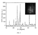
- FIG. 3 illustrates X-ray diffraction data for UD930, according to an embodiment of the invention.
- FIG. 4 illustrates a combined representation of an incident solar spectrum and measured absorption and emission spectra of UD930 in accordance with an embodiment of the invention.
- FIG. 5 through FIG. 8 illustrate manufacturing methods to form luminescent materials, according to some embodiments of the invention.
- FIG. 9 illustrates a solar module implemented in accordance with an embodiment of the invention.
- FIG. 10 illustrates measured photoluminescence intensity plotted as a function of annealing temperature for UD930, according to an embodiment of the invention.
- FIG. 11( a ) illustrates excitation spectra for UD930 at temperatures in the range of 12K to 300K, according to an embodiment of the invention.
- FIG. 11( b ) illustrates emission spectra for UD930 at temperatures in the range of 12K to 300K, according to an embodiment of the invention.
- a set refers to a collection of one or more elements.
- a set of layers can include a single layer or multiple layers.
- Elements of a set can also be referred to as members of the set.
- Elements of a set can be the same or different.
- elements of a set can share one or more common characteristics.
- Adjacent refers to being near or adjoining Adjacent elements can be spaced apart from one another or can be in actual or direct contact with one another. In some instances, adjacent elements can be connected to one another or can be formed integrally with one another.
- the terms “substantially” and “substantial” refer to a considerable degree or extent. When used in conjunction with an event or circumstance, the terms can refer to instances in which the event or circumstance occurs precisely as well as instances in which the event or circumstance occurs to a close approximation, such as accounting for typical tolerance levels of the embodiments described herein.
- the terms “optional” and “optionally” mean that the subsequently described event or circumstance may or may not occur and that the description includes instances where the event or circumstance occurs and instances in which it does not.
- a size of an object that is spherical can refer to a diameter of the object.
- a size of the non-spherical object can refer to a diameter of a corresponding spherical object, where the corresponding spherical object exhibits or has a particular set of derivable or measurable characteristics that are substantially the same as those of the non-spherical object.
- a size of a non-spherical object can refer to an average of various orthogonal dimensions of the object.
- a size of an object that is a spheroidal can refer to an average of a major axis and a minor axis of the object.
- the objects can have a distribution of sizes around the particular size.
- a size of a set of objects can refer to a typical size of a distribution of sizes, such as an average size, a median size, or a peak size.
- sub-micron range refers to a general range of dimensions less than about 1 ⁇ m or less than about 1,000 nm, such as less than about 999 nm, less than about 900 nm, less than about 800 nm, less than about 700 nm, less than about 600 nm, less than about 500 nm, less than about 400 nm, less than about 300 nm, or less than about 200 nm, and down to about 1 nm or less.
- the term can refer to a particular sub-range within the general range, such as from about 1 nm to about 100 nm, from about 100 nm to about 200 nm, from about 200 nm to about 300 nm, from about 300 nm to about 400 nm, from about 400 nm to about 500 nm, from about 500 nm to about 600 nm, from about 600 nm to about 700 nm, from about 700 nm to about 800 nm, from about 800 nm to about 900 nm, or from about 900 nm to about 999 nm.
- ultraviolet range refers to a range of wavelengths from about 5 nm to about 400 nm.
- visible range refers to a range of wavelengths from about 400 nm to about 700 nm.
- the term “infrared range” refers to a range of wavelengths from about 700 nm to about 2 mm.
- the infrared range includes the “near infrared range,” which refers to a range of wavelengths from about 700 nm to about 5 ⁇ m, the “middle infrared range,” which refers to a range of wavelengths from about 5 ⁇ m to about 30 ⁇ m, and the “far infrared range,” which refers to a range of wavelengths from about 30 ⁇ m to about 2 mm.
- the terms “reflection,” “reflect,” and “reflective” refer to a bending or a deflection of light
- the term “reflector” refers to an element that causes, induces, or is otherwise involved in such bending or deflection.
- a bending or a deflection of light can be substantially in a single direction, such as in the case of specular reflection, or can be in multiple directions, such as in the case of diffuse reflection or scattering.
- light incident upon a material and light reflected from the material can have wavelengths that are the same or different.
- Luminescence refers to an emission of light in response to an energy excitation.
- Luminescence can occur based on relaxation from excited electronic states of atoms or molecules and can include, for example, chemiluminescence, electroluminescence, photoluminescence, thermoluminescence, triboluminescence, and combinations thereof.
- Luminescence can also occur based on relaxation from excited states of quasi-particles, such as excitons, bi-excitons, and exciton-polaritons.
- photoluminescence which can include fluorescence and phosphorescence
- an excited state can be produced based on a light excitation, such as absorption of light.
- light incident upon a material and light emitted by the material can have wavelengths that are the same or different.
- optical quantum efficiency refers to a ratio of the number of photons emitted by a photoluminescent material to the number of photons absorbed by the photoluminescent material.
- absorption spectrum refers to a representation of absorption of light over a range of wavelengths.
- an absorption spectrum can refer to a plot of absorbance (or transmittance) of a material as a function of wavelength of light incident upon the material.
- emission spectrum refers to a representation of emission of light over a range of wavelengths.
- an emission spectrum can refer to a plot of intensity of light emitted by a material as a function of wavelength of the emitted light.
- excitation spectrum refers to another representation of emission of light over a range of wavelengths.
- an excitation spectrum can refer to a plot of intensity of light emitted by a material as a function of wavelength of light incident upon the material.
- FWHM Full Width at Half Maximum
- a FWHM can refer to a width of a spectrum at half of a peak intensity value.
- substantially flat refers to being substantially invariant with respect to a change in wavelength.
- a photoluminescent characteristic can be referred to as being substantially flat over a range of wavelengths if values of that characteristic within that range of wavelengths exhibit a standard deviation of less than 20 percent with respect to an average value, such as less than 10 percent or less than 5 percent.
- an emission spectrum refers to emission of light over a narrow range of wavelengths.
- an emission spectrum can be referred to as being substantially monochromatic if a spectral width is no greater than 120 nm at FWHM, such as no greater than 100 nm at FWHM, no greater than 80 nm at FWHM, or no greater than 50 nm at FWHM.
- dopant refers to a chemical entity that is present in a material as an additive or an impurity.
- the presence of a dopant in a material can alter a set of characteristics of the material, such as its chemical, magnetic, electronic, or optical characteristics.
- the term “electron acceptor” refers to a chemical entity that has a tendency to attract an electron from another chemical entity
- the term “electron donor” refers to a chemical entity that has a tendency to provide an electron to another chemical entity.
- an electron acceptor can have a tendency to attract an electron from an electron donor. It should be recognized that electron attracting and electron providing characteristics of a chemical entity are relative.
- a chemical entity that serves as an electron acceptor in one instance can serve as an electron donor in another instance.
- electron acceptors include positively charged chemical entities and chemical entities including atoms with relatively high electronegativities.
- Examples of electron donors include negatively charged chemical entities and chemical entities including atoms with relatively low electronegativities.
- a set of characteristics of a material can sometimes vary with temperature. Unless otherwise specified herein, a characteristic of a material can be specified at room temperature, such as 300K or 27° C.
- Embodiments of the invention relate to luminescent materials having a number of desirable characteristics.
- luminescent materials according to some embodiments of the invention can exhibit photoluminescence with a high quantum efficiency, with a narrow spectral width, and with a peak emission wavelength located within a desirable range of wavelengths.
- these photoluminescent characteristics can be relatively insensitive over a wide range of excitation wavelengths.
- these unusual and desirable characteristics can at least partly derive from a particular microstructure of the luminescent materials.
- the luminescent materials can be inexpensively and readily processed to form a variety of products, which, in turn, can be used in solar modules and other applications.
- Desirable luminescent materials include a class of semiconductor materials that can be represented with reference to the formula: [A a B b X x ][dopants] (1)
- A is selected from elements of Group 1, such as sodium (e.g., as Na(I) or Na +1 ), potassium (e.g., as K(I) or K +1 ), rubidium (e.g., as Rb(I) or Rb +1 ), and cesium (e.g., as Cs(I) or Cs +1 );
- B is selected from elements of Group 5, such as vanadium (e.g., as V(III) or V +3 ), elements of Group 11, such as copper (e.g., as Cu(I) or Cu +1 ), silver (e.g., as Ag(I) or Ag +1 ), and gold (e.g., as Au(I) or Au +1 ), elements of Group 12, such as zinc (e.g., as Zn(II) or Zn +2 ), cadmium (e.g., as Cd(II) or Cd +2 ), and mercury (e.g., as Hg(II) or Hg +
- a is an integer that can be in the range of 1 to 12, such as from 1 to 8 or from 1 to 5; b is an integer that can be in the range of 1 to 8, such as from 1 to 5 or from 1 to 3; and x is an integer that can be in the range of 1 to 12, such as from 1 to 8 or from 1 to 5.
- x can be equal to a+2b, such as for purposes of charge balance when oxidation states of A, B, and X are +1, +2, and ⁇ 1, respectively.
- a can be equal to 1
- x can be equal to 1+2b. It is also contemplated that one or more of a, b, and x can have fractional values within their respective ranges.
- X x in formula (1) can be more generally represented as X x X′ x′ (or X x X′ x′ X′′ x′′ ), where X and X′ (or X, X′, and X′′) can be independently selected from elements of Group 17, and the sum of x and x′ (or the sum of x, x′, and x′′) can be in the range of 1 to 12, such as from 1 to 9 or from 1 to 5.
- the sum of x and x′ (or the sum of x, x′, and x′′) can be equal to a+2b.
- a can be equal to 1, and the sum of x and x′ (or the sum of x, x′, and x′′) can be equal to 1+2b. It is further contemplated that a blend or a mixture of different luminescent materials represented by formula (1) can be used.
- Dopants can be optionally included in a luminescent material represented by formula (1), and can be present in amounts that are less than about 5 percent, such as less than about 1 percent or from about 0.1 percent to about 1 percent, in terms of atomic percent or elemental composition.
- the dopants can derive from reactants that are used to form the luminescent material, or can derive from moisture, atmospheric gases, or other chemical entities present during the formation of the luminescent material.
- the dopants can include cations, anions, or both, which can form electron acceptor/electron donor pairs that are dispersed within a microstructure of the luminescent material.
- Examples of luminescent materials represented by formula (1) include those represented with reference to the formula: [A a Sn b X x ][dopants] (2)
- A is selected from potassium, rubidium, and cesium; and X is selected from chlorine, bromine, and iodine. Still referring to formula (2), x can be equal to a+2b. In some instances, a can be equal to 1, and x can be equal to 1+2b.
- Several luminescent materials with desirable characteristics can be represented as CsSnX 3 [dopants] and include materials designated as UD700 and UD930. In the case of UD700, X is bromine, and, in the case of UD930, X is iodine. UD700 exhibits a peak emission wavelength at about 695 nm, while UD930 exhibits a peak emission wavelength at about 950 nm.
- the spectral width of UD700 and UD930 is narrow (e.g., about 50 meV or less at FWHM), and the absorption spectrum is substantially flat from the absorption edge into the far ultraviolet.
- Photoluminescent emission of UD700 and UD930 is stimulated by a wide range of wavelengths of solar radiation up to the absorption edge of these materials at about 695 nm for UD700 and about 950 nm for UD930.
- the chloride analog namely CsSnCl 3 [dopants] exhibits a peak emission wavelength at about 450 nm, and can be desirable for certain implementations.
- FIG. 1 Normalized emission spectra of UD700, UD930, and the chloride analog, as measured using a xenon lamp source at about 300K, are illustrated in FIG. 1 in accordance with an embodiment of the invention.
- Other luminescent materials with desirable characteristics include CsSn 2 X 5 [dopants], Cs 2 SnX 4 [dopants], and CsSn 3 X 7 [dopants], mixtures thereof with, or without, CsSnX 3 [dopants], such as a mixture of CsSnX 3 [dopants], CsSn 2 X 5 [dopants], and Cs 2 SnX 4 [dopants], and luminescent materials in which at least a fraction of cesium is substituted with another monovalent ion of comparable size, such as CH 3 NH 3 + or other poly-elemental, monovalent ions.
- Additional luminescent materials with desirable characteristics include RbSnX 3 [dopants], such as RbSnI 3 [dopants] that exhibits a peak emission wavelength at about 705 nm, and RbSnBr 3 [dopants] that exhibits a peak emission wavelength at about 540 nm.
- Further luminescent materials with desirable characteristics include KSnX 3 [dopants], such as KSnBr 3 [dopants] that exhibits a peak emission wavelength at about 465 nm.
- Each of these luminescent materials can be deposited as a film in a single layer or in multiple layers interspersed with other layers formed from the same luminescent material or different luminescent materials.
- luminescent materials represented by formula (1) include those represented with reference to the formula: [A a Ge b X x ][dopants] (3)
- A is selected from potassium, rubidium, and cesium; and X is selected from chlorine, bromine, and iodine. Still referring to formula (3), x can be equal to a+2b. In some instances, a can be equal to 1, and x can be equal to 1+2b. In the case that A is cesium, and X is iodine, for example, a luminescent material can sometimes be represented with reference to the formula: [CsGeI 3 ][dopants] (4)
- luminescent materials represented by formula (1) include those represented with reference to the formula: [A a Pb b X x ][dopants] (5)
- A is selected from potassium, rubidium, and cesium; and X is selected from chlorine, bromine, and iodine. Still referring to formula (5), x can be equal to a+2b. In some instances, a can be equal to 1, and x can be equal to 1+2b. In the case that A is cesium, and X is iodine, for example, a luminescent material can sometimes be represented with reference to the formula: [CsPbI 3 ][dopants] (6)
- luminescent materials represented by formula (1) include those represented with reference to the formula: [A a Sn b X x X′ x′ ][dopants] (7)
- A is selected from potassium, rubidium, and cesium; and X and X′ are different and are selected from fluorine, chlorine, bromine, and iodine. Still referring to formula (7), the sum of x and x′ can be equal to a+2b.
- at least one of X and X′ can be iodine, which can constitute at least 1 ⁇ 5, at least 1 ⁇ 4, at least 1 ⁇ 3, at least 1 ⁇ 2, or at least 2 ⁇ 3 of a total number of halide ions.
- a can be equal to 1
- the sum of x and x′ can be equal to 1+2b.
- a luminescent material can sometimes be represented with reference to one of the formulas: [CsSnClI 2 ][dopants] (8) [CsSnCl 2 I][dopants] (9) [CsSn 2 Cl 2 I 3 ][dopants] (10) [CsSn 2 Cl 3 I 2 ][dopants] (11) [CsSn 2 ClI 4 ][dopants] (12) [CsSn 2 Cl 4 I][dopants] (13) [Cs 2 SnClI 3 ][dopants] (14) [Cs 2 SnCl 2 I 2 ][dopants] (15) [Cs 2 SnCl 3 I][dopants] (16) And, in the case that A is cesium, X is bromine, and X′ is iodine, for example, a luminescent material can sometimes be represented with reference to one of the formulas: [CsSnClI 2 ]
- luminescent materials represented by formula (1) include those represented with reference to the formula: [A a Sn b X x X′ x′ X′′ x′′ ][dopants] (35)
- A is selected from potassium, rubidium, and cesium; and X, X′, and X′′ are different and are selected from fluorine, chlorine, bromine, and iodine. Still referring to formula (35), the sum of x, x′, and x′′ can be equal to a+2b. In order to achieve desirable photoluminescent characteristics, at least one of X, X′, and X′′ can be iodine, which can constitute at least 1 ⁇ 5, at least 1 ⁇ 4, at least 1 ⁇ 3, at least 1 ⁇ 2, or at least 2 ⁇ 3 of a total number of halide ions.
- a can be equal to 1
- the sum of x, x′, and x′′ can be equal to 1+2b.
- Certain luminescent materials represented by formula (1) can have a perovskite-based microstructure.
- This perovskite-based microstructure can be layered with relatively stronger chemical bonding within a particular layer and relatively weaker chemical bonding between different layers.
- certain luminescent materials represented by formula (1) can have a perovskite-based crystal structure.
- This structure can be arranged in the form of a network of BX 6 octahedral units along different planes, with B at the center of each octahedral unit and surrounded by X, and with A interstitial between the planes, as illustrated in FIG.
- X is a monovalent anion
- A is a cation that serves to balance the total charge and to stabilize the crystal structure.
- dopants can be incorporated in a perovskite-based crystal structure, as manifested by, for example, substitution of a set of atoms included in the structure with a set of dopants.
- Cs +1 and Sn +2 can be substituted with a cation such as Sn(IV) or Sn +4
- I ⁇ 1 can be substituted with an anion such as F ⁇ 1 , Cl ⁇ 1 , Br ⁇ 1 , O ⁇ 2 , OH ⁇ 1 , or other anions with smaller radii relative to I ⁇ 1 .
- the incorporation of dopants can alter a perovskite-based crystal structure relative to the absence of the dopants, as manifested by, for example, shorter bond lengths along a particular plane and between different planes, such as shorter B—X—B bond lengths along a particular plane and shorter B—X—B bond lengths between different planes.
- substitution of I ⁇ 1 with either, or both, of F ⁇ 1 and Cl ⁇ 1 can lead to shorter and stronger bonds with respect to Sn ⁇ 2 along a particular plane and between different planes.
- the incorporation of dopants can lend greater stability to a perovskite-based crystal structure, and desirable photoluminescent characteristics can at least partly derive from the presence of these dopants.
- substitution of I ⁇ 1 with other halides can be at levels greater than typical doping levels, such as up to about 50 percent of I ⁇ 1 to form an alloy of mixed halides.
- Certain luminescent materials represented by formula (1) can be polycrystalline with constituent crystallites or grains having sizes in the sub-micron range.
- the configuration of grains can vary from one that is quasi-isotropic, namely in which the grains are relatively uniform in shape and size and exhibit a relatively uniform grain boundary orientation, to one that is anisotropic, namely in which the grains exhibit relatively large deviations in terms of shape, size, grain boundary orientation, texture, or a combination thereof.
- grains can be formed in an anisotropic fashion and with an average size in the range of about 200 nm to about 400 nm, such as from about 250 nm to about 350 nm.
- the luminescent materials represented by formula (1) have characteristics that are desirable for solar modules.
- the luminescent materials can exhibit photoluminescence with a high optical quantum efficiency that is greater than about 6 percent, such as at least about 10 percent, at least about 20 percent, at least about 25 percent, at least about 30 percent, or at least about 35 percent, and can be up to about 40 percent, about 50 percent, or more, and with a high internal quantum efficiency that is greater than about 50 percent, such as at least about 60 percent, at least about 70 percent, at least about 75 percent, at least about 80 percent, or at least about 85 percent, and can be up to about 95 percent, about 99 percent, or more.
- the luminescent materials can exhibit photoluminescence with a narrow spectral width that is no greater than about 120 nm at FWHM, such as no greater than about 100 nm or no greater than about 80 nm at FWHM.
- the spectral width can be in the range of about 20 nm to about 120 nm at FWHM, such as from about 50 nm to about 120 nm, from about 50 nm to about 100 nm, or from about 50 nm to about 80 nm at FWHM.
- Incorporation of the luminescent materials within a resonant cavity waveguide can further narrow the spectral width.
- the luminescent materials can have bandgap energies and resistivities that are tunable to desirable levels by adjusting reactants and processing conditions that are used.
- a bandgap energy can correlate with A, with the order of increasing bandgap energy corresponding to, for example, cesium, rubidium, potassium, and sodium.
- the bandgap energy can correlate with X, with the order of increasing bandgap energy corresponding to, for example, iodine, bromine, chlorine, and fluorine. This order of increasing bandgap energy can translate into an order of decreasing peak emission wavelength.
- a luminescent material including iodine can sometimes exhibit a peak emission wavelength in the range of about 900 nm to about 1 ⁇ m, while a luminescent material including bromine or chlorine can sometimes exhibit a peak emission wavelength in the range of about 700 nm to about 800 nm.
- the resulting photoluminescence can have a peak emission wavelength located within a desirable range of wavelengths, such as the visible range or the infrared range.
- the peak emission wavelength can be located in the near infrared range, such as from about 900 nm to about 1 ⁇ m, from about 910 nm to about 1 ⁇ m, from about 910 nm to about 980 nm, or from about 930 nm to about 980 nm.
- the photoluminescence characteristics described above can be relatively insensitive over a wide range of excitation wavelengths. Indeed, this unusual characteristic can be appreciated with reference to excitation spectra of the luminescent materials, which excitation spectra can be substantially flat over a range of excitation wavelengths encompassing portions of the ultraviolet range, the visible range, and the infrared range. In some instances, the excitation spectra can be substantially flat over a range of excitation wavelengths from about 200 nm to about 1 ⁇ m, such as from about 200 nm to about 980 nm or from about 200 nm to about 950 nm.
- absorption spectra of the luminescent materials can be substantially flat over a range of excitation wavelengths encompassing portions of the ultraviolet range, the visible range, and the infrared range. In some instances, the absorption spectra can be substantially flat over a range of excitation wavelengths from about 200 nm to about 1 ⁇ m, such as from about 200 nm to about 980 nm or from about 200 nm to about 950 nm. Also, optical quantum efficiencies of the luminescent materials can be substantially flat over a range of excitation wavelengths, such as from about 200 nm to about 1 ⁇ m, from about 200 nm to about 980 nm or from about 450 nm to about 900 nm.
- UD930 has a direct bandgap with a value of about 1.32 eV at 300K. This bandgap can decrease as temperature decreases, at least partly resulting from an harmonicity in a lattice potential.
- photoluminescence for UD930 can occur via exciton emission.
- An exciton corresponds to an electron-hole pair, which can be formed as a result of light absorption.
- Most semiconductor materials have relatively small exciton binding energies, so excitons are typically not present at room temperature.
- Certain luminescent materials represented by formula (1) can have relatively large exciton binding energies, and can be incorporated in a resonant cavity waveguide to yield suppression of emission in a vertical direction and stimulated emission along a plane of the cavity waveguide.
- the cavity waveguide can be readily formed in an inexpensive manner, without resorting to techniques such as Molecular Beam Epitaxy (“MBE”).
- MBE Molecular Beam Epitaxy
- FIG. 4 illustrates a combined representation of a solar spectrum and measured absorption and emission spectra of UD930 in accordance with an embodiment of the invention.
- FIG. 4 illustrates the AM1.5G solar spectrum (referenced as (A)), which is a standard solar spectrum representing incident solar radiation on the surface of the earth.
- the AM1.5G solar spectrum has a gap in the region of 930 nm due to atmospheric absorption.
- the absorption spectrum (referenced as (B)) and emission spectrum (referenced as (C)) of UD930 render this material particularly effective for spectral concentration when incorporated within an emission layer.
- photoluminescence of UD930 is substantially located in the gap of the AM1.5G solar spectrum, with the peak emission wavelength of about 950 nm falling within the gap.
- This allows the use of reflector layers (e.g., above and below the emission layer) that are tuned to reflect emitted radiation back towards the emission layer, without significant reduction of incident solar radiation that can pass through the reflector layers and reach UD930.
- the absorption spectrum of UD930 is substantially flat and extends from the absorption edge at about 950 nm through a large fraction of the AM1.5G solar spectrum into the ultraviolet.
- the peak emission wavelength of about 950 nm is matched to the absorption edge of PV cells based on silicon, and the spectral width is about 50 meV at FWHM (or about 37 nm at FWHM).
- the absorption coefficient of silicon is about 10 2 cm ⁇ 1 in this range of emission wavelengths, and junctions within the PV cells can be designed to efficiently absorb the emitted radiation and convert the radiation into electron-hole pairs.
- UD930 can broadly absorb a wide range of wavelengths from incident solar radiation, while emitting a narrow range of wavelengths that are matched to silicon to allow a high conversion efficiency of incident solar radiation into electricity.
- the absorption spectrum and the emission spectrum of UD930 overlap to a low degree, thereby reducing instances of self-absorption that would otherwise lead to reduced conversion efficiency.
- Luminescent materials represented by formula (1) can be formed via reaction of a set of reactants or precursors at high yields and at moderate temperatures and pressures.
- the reaction can be represented with reference to the formula: Source(B)+Source(A, X) ⁇ Luminescent Material (48)
- source(B) serves as a source of B, and, in some instances, source(B) can also serve as a source of dopants or halide ions.
- source(B) can include one or more types of B-containing compounds selected from B(II) compounds of the form BY, BY 2 , B 3 Y 2 , and B 2 Y and B(IV) compounds of the form BY 4 , where Y can be selected from elements of Group 16, such as oxygen (e.g., as O ⁇ 2 ); elements of Group 17, such as fluorine (e.g., as F ⁇ 1 ), chlorine (e.g., as Cl ⁇ 1 ), bromine (e.g., as Br ⁇ 1 ), and iodine (e.g., as I ⁇ 1 ); and poly-elemental chemical entities, such as nitrate (i.e., NO 3 ⁇ 1 ), thiocyanate (i
- tin(II) compounds include tin(II) fluoride (i.e., SnF 2 ), tin(II) chloride (i.e., SnCl 2 ), tin(II) chloride dihydrate (i.e., SnCl 2 .2H 2 O), tin(II) bromide (i.e., SnBr 2 ), tin(II) iodide (i.e., SnI 2 ), tin(II) oxide (i.e., SnO), tin(II) sulfate (i.e., SnSO 4 ), tin(II) orthophosphate (i.e., Sn 3 (PO 4 ) 2 ), tin(II) metaphosphate (i.e., Sn(PO 3 ) 2 ), tin(II) oxalate (i.e., Sn(C 2 O 4 )), t
- tin (IV) compounds include tin(IV) chloride (i.e., SnCl 4 ) and tin(IV) chloride pentahydrate (i.e., SnCl 4 .5H 2 O). It is contemplated that different types of source(B) can be used, such as source(B) and source(B′), with B and B′ independently selected from elements of Group 14, or as source(B), source(B′), and source(B′′), with B, B′, and B′′ independently selected from elements of Group 14.
- source(A, X) serves as a source of A and X, and, in some instances, source(A, X) can also serve as a source of dopants.
- Examples of source(A, X) include alkali halides of the form AX.
- source(A, X) can include one or more types of A(I) halides, such as cesium(I) fluoride (i.e., CsF), cesium(I) chloride (i.e., CsCl), cesium(I) bromide (i.e., CsBr), cesium(I) iodide (i.e., CsI), potassium(I) fluoride (i.e., KF), potassium(I) chloride (i.e., KCl), potassium(I) bromide (i.e., KBr), potassium(I) iodide (i.e., KI), rubidium(I) fluoride (i.e., RbF), rubidium(I) chloride (i.e., RbCl), rubidium(I) bromide (i.e., RbBr), and rubidium(I) iodide
- CsF cesium(I) fluoride
- source(A, X) can be used, such as source(A, X) and source(A′, X′), with A and A′ independently selected from elements of Group 1, and X and X′ independently selected from elements of Group 17, or as source(A, X), source(A′, X′), and source(A′′, X′′), with A, A′, and A′′ independently selected from elements of Group 1, and X, X′, and X′′ independently selected from elements of Group 17.
- the reaction represented by formula (48) can be carried out by combining, mixing, or otherwise contacting source(B) with source(A, X), and then applying a form of energy.
- source(B) and source(A, X) can be deposited on a substrate to form a set of films or layers.
- source(B) and source(A, X) can be co-deposited on a substrate to form a film, or can be sequentially deposited to form adjacent films.
- source(B) and source(A, X) can be mixed in a dry form, in solution, or in accordance with any other suitable mixing technique.
- source(B) and source(A, X) can be provided in a powdered form, and can be mixed using any suitable dry mixing technique.
- source(B) and source(A, X) can be dispersed in a reaction medium to form a reaction mixture, and the reaction medium can include a solvent or a mixture of solvents.
- a form of energy is applied to promote formation of a luminescent material, such as in the form of acoustic or vibrational energy, electrical energy, magnetic energy, mechanical energy, optical energy, or thermal energy.
- source(B) and source(A, X) can be deposited on a substrate, and a resulting set of films can be heated to a suitable temperature to form the luminescent material. Heating can be performed in air, in an inert atmosphere (e.g., a nitrogen atmosphere), or in a reducing atmosphere for a suitable time period. It is also contemplated that multiple forms of energy can be applied simultaneously or sequentially.
- the resulting luminescent material can include A, B, and X as major elemental components as well as elemental components derived from or corresponding to Y.
- the luminescent material can include additional elemental components, such as carbon, chlorine, hydrogen, and oxygen, that can be present in amounts that are less than about 5 percent or less than about 1 percent in terms of elemental composition, and further elemental components, such as sodium, sulfur, phosphorus, and potassium, that can be present in trace amounts that are less than about 0.1 percent in terms of elemental composition.
- reaction represented by formula (48) examples include those represented with reference to the formula: BY 2 +AX ⁇ Luminescent Material (49)
- B is selected from germanium, tin, and lead; Y is selected from fluorine, chlorine, bromine, and iodine; A is selected from potassium, rubidium, and cesium; and X is selected from fluorine, chlorine, bromine, and iodine.
- BY 2 can be more generally represented as BY 2 and B′Y′ 2 (or BY 2 , B′Y′ 2 , and B′′Y′′ 2 ), where B and B′ (or B, B′, and B′′) are independently selected from germanium, tin, and lead, and Y and Y′ (or Y, Y′, and Y′′) are independently selected from fluorine, chlorine, bromine, and iodine.
- BY 2 can be represented as SnY 2 , or can be more generally represented as SnY 2 and SnY′ 2 (or SnY 2 , SnY′ 2 , and SnY′′ 2 ), where Y and Y′ (or Y, Y′, and Y′′) are independently selected from fluorine, chlorine, bromine, and iodine.
- SnI 2 (or SnCl 2 ) can be reacted with CsI to form a luminescent material having a peak emission wavelength at about 950 nm, such as UD930.
- SnBr 2 can be reacted with CsBr to form a luminescent material having a peak emission wavelength at about 695 nm, such as UD700.
- SnBr 2 can be reacted with KBr to form a luminescent material having a peak emission wavelength at about 465 nm.
- SnI 2 can be reacted with RbI to form a luminescent material having a peak emission wavelength at about 705 nm.
- SnBr 2 can be reacted with RbBr to form a luminescent material having a peak emission wavelength at about 540 nm.
- FIG. 5 through FIG. 8 illustrate manufacturing methods to form luminescent materials, according to some embodiments of the invention.
- a substrate 500 is provided.
- the substrate 500 serves as a supporting structure during manufacturing operations, and serves to protect a resulting luminescent material from environmental conditions.
- the substrate 500 can be rigid or flexible, can be porous or non-porous, can be optically transparent, translucent, or opaque, and can be formed from a glass, a metal, a ceramic, a polymer, or another suitable material.
- the substrate 500 can include a base substrate and a set of coatings or films that are formed adjacent to the base substrate to provide a deposition surface for subsequent manufacturing operations.
- suitable coating materials include oxides, such as silica (i.e., SiO 2 or ⁇ -SiO 2 ), alumina (i.e., Al 2 O 3 ), TiO 2 , Ta 2 O 5 , Nb 2 O 5 , ZrO 2 , HfO 2 , SnO 2 , ZnO 2 , La 2 O 3 , Y 2 O 3 , CeO 2 , Sc 2 O 3 , Er 2 O 3 , V 2 O 5 , and In 2 O 3 ; and other suitable thin-film dielectric materials.
- oxides such as silica (i.e., SiO 2 or ⁇ -SiO 2 ), alumina (i.e., Al 2 O 3 ), TiO 2 , Ta 2 O 5 , Nb 2 O 5 , ZrO 2 , HfO 2 , SnO 2 , ZnO 2 , La 2 O 3 , Y 2 O 3 , CeO 2 , Sc 2 O 3 , Er 2 O 3
- Substrate effects can sometimes occur with respect to resulting photoluminescence characteristics. For example, enhancements of about three times or more in photoluminescence intensity, such as from about 5 times to about 10 times, can occur for alumina-based ceramic substrates, relative to substrates formed from certain other materials. Without being bound by a particular theory, such enhancements can at least partly derive from one or a combination of the following: a R1 R2 emission process; surface roughness of the alumina-based ceramic substrate; and high reflectivity of the alumina-based ceramic substrate, which can promote reflection of incident radiation back towards a luminescent material.
- a set of reactants that are precursors of a luminescent material
- source(B) and source(A, X) are subjected to vacuum deposition, thereby forming a precursor layer 502 adjacent to the substrate 500 .
- Deposition can be carried out using a vacuum deposition system that is evacuated to a pressure no greater than about 1 ⁇ 10 ⁇ 4 Torr, such as no greater than about 1 ⁇ 10 ⁇ 5 Torr, and down to about 1 ⁇ 10 ⁇ 6 Torr or less. It is contemplated that another suitable deposition technique can be used in place of, or in conjunction with, vacuum deposition.
- Source(B) and source(A, X) can be carried out sequentially in accordance with the same vacuum deposition technique or different vacuum deposition techniques.
- BY 2 and AX can be evaporated in sequential layers, from two layers to 30 or more layers total, such as from two layers to 16 layers total, or from two layers to six layers total, and with a weight or molar ratio of BY 2 to AX from about 99:1 to about 1:99, such as from about 5:1 to about 1:5 or from about 2:1 to about 1:2.
- a particular one of BY 2 and AX having a lower melting point T m1 can be placed in an evaporator boat and deposited by thermal evaporation, while another one of BY 2 and AX having a higher melting point T m2 can be placed in another evaporator boat and deposited by thermal evaporation or electron-beam evaporation.
- SnI 2 (or SnCl 2 with a melting point of about 246° C.) and CsI with a melting point of about 620° C.
- SnI 2 (or SnCl 2 ) can be deposited by thermal evaporation, while CsI can be deposited by thermal evaporation or electron-beam evaporation.
- a thickness of each individual BY 2 -containing layer or each individual AX-containing layer can be in the range of about 10 nm to about 1.5 ⁇ m, such as from about 10 nm to about 1 ⁇ m or from about 10 nm to about 300 nm, with a total thickness for all layers in the range of about 20 nm to about 45 ⁇ m, such as from about 40 nm to about 20 ⁇ m or from about 50 nm to about 5 ⁇ m.
- Source(B) and source(A, X) can also be co-deposited in accordance with a particular vacuum deposition technique.
- BY 2 and AX can be co-evaporated to form a single layer or multiple layers, with a weight or molar ratio of BY 2 to AX from about 10:1 to about 1:10, such as from about 5:1 to about 1:5 or from about 2:1 to about 1:2, and with a total thickness in the range of about 10 nm to about 1.5 ⁇ m, such as from about 10 nm to about 1 ⁇ m or from about 10 nm to about 300 nm.
- BY 2 and AX can be mixed in an evaporator boat and then deposited by thermal evaporation.
- BY 2 and AX can be carried out in a powdered form, or by forming a pre-melt of BY 2 and AX.
- SnI 2 or SnCl 2
- CsI SnI 2
- SnCl 2 can evaporate at lower temperatures than CsI, and, therefore, a temperature of the evaporator boat can be gradually raised as a relative amount of CsI in a mixture increases.
- source(B) can be co-deposited with source(A, X) or deposited sequentially with source(A, X).
- BY 2 and B′Y′ 2 can be mixed in an evaporator boat and deposited by thermal evaporation, followed by deposition of AX, and so forth.
- Mixing of BY 2 and B′Y′ 2 can be carried out in a powdered form, or by forming a pre-melt of BY 2 and B′Y′ 2 , with a weight or molar ratio of BY 2 to B′Y′ 2 from about 99:1 to about 1:99, such as from about 5:1 to about 1:5 or from about 2:1 to about 1:2.
- BY 2 , B′Y′ 2 , and B′′Y′′ 2 can be mixed in an evaporator boat and deposited by thermal evaporation, followed by deposition of AX, and so forth.
- different types of source(A, X) can be used, and can be co-deposited with source(B) or deposited sequentially with source(B).
- an encapsulation material is next deposited, thereby forming an encapsulation layer 504 adjacent to the precursor layer 502 .
- the encapsulation layer 504 serves to provide protection and sealing of a resulting luminescent material and to reduce its exposure to oxygen, humidity, and other contaminants, thereby enhancing stability of resulting photoluminescence characteristics.
- suitable encapsulation materials include oxides, such as silica, alumina, TiO 2 , Ta 2 O 5 , Nb 2 O 5 , ZrO 2 , HfO 2 , SnO 2 , ZnO 2 , La 2 O 3 , Y 2 O 3 , CeO 2 , Sc 2 O 3 , Er 2 O 3 , V 2 O 5 , and In 2 O 3 ; nitrides, such as SiO x N 2-x ; fluorides, such as CaF 2 , SrF 2 , ZnF 2 , MgF 2 , LaF 3 , and GdF 2 ; nanolaminates, such as HfO 2 /Ta 2 O 5 , TiO 2 /Ta 2 O 5 , TiO 2 /Al 2 O 3 , ZnS/Al 2 O 3 , and AlTiO; and other suitable thin-film dielectric materials.
- oxides such as silica, alumina, TiO 2 , Ta
- suitable encapsulation materials include glasses, such as borosilicate glasses (e.g., Borofloat® glass and D 263TM glass), phosphate glasses, and other low melting glasses.
- a thickness of the encapsulation layer 504 can be in the range of about 10 nm to about 1.5 ⁇ m, such as from about 50 nm to about 500 nm or from about 50 nm to about 300 nm.
- a suitable metal can be deposited adjacent to the layer of glass to provide a hermetic seal, such as silver, aluminum, gold, copper, iron, cobalt, nickel, palladium, platinum, ruthenium, or iridium.
- Vacuum deposition such as electron-beam evaporation, can be used to form the encapsulation layer 504 , along with the other layers of the assembly of layers.
- another suitable deposition technique can be used, such as sputtering.
- the assembly of layers is next subjected to annealing to promote bonding between the layers as well as to promote reaction according to formula (48), thereby converting the precursor layer 502 to an emission layer including a luminescent material according to formula (1).
- Annealing can be carried out using any suitable heating technique to apply thermal energy via conduction, convection, or radiation heating, such as by heating the assembly of layers using a hot plate, an oven, resist heating, or lamp heating. It is also contemplated that thermal energy can be applied in accordance with fast heating cycles to yield rapid thermal annealing.
- Resulting photoluminescence characteristics can be dependent upon an annealing temperature and an annealing time period.
- an annealing temperature and an annealing time period can be optimized to yield higher photoluminescence intensities.
- a particular one of BY 2 and AX can have a lower melting point T m1
- another one of BY 2 and AX can have a higher melting point T m2
- an optimal annealing temperature T heat can be greater than T m1 and less than T m2 , such as greater than T m1 and up to a three-quarters point (i.e., (T m1 +3T m2 )/4) or a halfway point (i.e., (T m1 +T m2 )/2) between the lower melting point and the higher melting point, although annealing can also be carried out at higher or lower temperatures.
- an optimal annealing temperature T heat can be greater than about 318° C. and less than about 620° C., such as from about 340° C. to about 420° C. or from about 350° C. to about 410° C.
- an optimal annealing temperature T heat can be greater than about 246° C. and less than about 620° C.
- an initial melting can arise from formation of an eutectic between SnCl 2 and a reaction product of SnCl 2 and CsI.
- An optimal annealing time period can be in the range of about 1 sec to about 1 hr, such as from about 5 sec to about 10 min or from about 5 sec to about 1 min, although annealing can also be carried out for longer or shorter time periods.
- Optimal values of an annealing temperature and an annealing time period can also be suitably adjusted depending upon, for example, particular reagents used, a thickness of individual layers within the precursor layer 502 , or a total thickness of the precursor layer 502 .
- a reaction between layers of reactants can occur at temperatures significantly below melting temperatures of the reactants by way of solid state reactions.
- the layers can be sufficiently thin so that diffusion can occur within, for example, a few hundred nanometers or less and a time period of a few seconds to a few minutes, thereby allowing the reactants to react and to form a luminescent material.
- a substrate 600 is provided, and a precursor layer 604 is formed adjacent to the substrate 600 .
- Certain aspects of the manufacturing method of FIG. 6 can be implemented in a similar manner as described above for FIG. 5 , and, therefore, are not further described herein.
- a reflector layer 602 is initially formed adjacent to the substrate 600 , followed by formation of the precursor layer 604 adjacent to the reflector layer 602 , and followed by formation of another reflector layer 606 adjacent to the precursor layer 604 .
- the pair of reflector layers 602 and 606 serve to provide protection and sealing of a resulting luminescent material and to reduce its exposure to oxygen, humidity, and other contaminants.
- the pair of reflector layers 602 and 606 serve to reduce loss of emitted radiation and to promote guiding of the emitted radiation along a lateral direction.
- each of the reflector layers 602 and 606 is implemented as a dielectric stack, including multiple dielectric layers and with the number of dielectric layers in the range of 2 to 1,000, such as in the range of 2 to 100, in the range of 30 to 80, or in the range of 30 to 80.
- Each individual dielectric layer can have a thickness in the range of about 1 nm to about 200 nm, such as from about 10 nm to about 150 nm or from about 10 nm to about 100 ⁇ m.
- a total thickness of each of the reflector layers 602 and 606 can be in the range of about 100 nm to about 20 ⁇ m, such as from about 1 ⁇ m to about 15 ⁇ m or from about 1 ⁇ m to about 10 ⁇ m.
- a dielectric stack can include multiple layers formed from different dielectric materials. Layers formed from different materials can be arranged in a periodic fashion, such as in an alternating fashion, or in a non-periodic fashion.
- oxides such as si
- different materials forming a dielectric stack have different refractive indices so as to form a set of high index layers and a set of low index layers that are interspersed within the dielectric stack.
- an index contrast in the range of about 0.3 to about 1 or in the range of about 0.3 to about 2 can be desirable.
- TiO 2 and SiO 2 can be included in alternating layers of a dielectric stack to provide a relatively large index contrast between the layers.
- a larger index contrast can yield a larger stop band with respect to emitted radiation, thereby approaching the performance of an ideal omnireflector.
- a larger index contrast can yield a greater angular tolerance for reflectivity with respect to incident solar radiation, and can reduce a leakage of emitted radiation at larger angles from a normal direction.
- the assembly of layers illustrated in FIG. 6 is then subjected to annealing to promote bonding between the layers as well as to promote reaction according to formula (48), thereby converting the precursor layer 604 to an emission layer that is sandwiched between the reflector layers 602 and 606 .
- a reflector layer 702 is formed adjacent to a substrate 700 , and a precursor layer 704 is formed adjacent to the reflector layer 702 .
- Certain aspects of the manufacturing method of FIG. 7 can be implemented in a similar manner as described above for FIG. 5 and FIG. 6 , and, therefore, are not further described herein.
- a spacer layer 706 is next formed adjacent to the precursor layer 704 , followed by formation of another reflector layer 708 adjacent to the spacer layer 706 .
- the spacer layer 706 and the reflector layer 708 serve to provide protection and sealing of a resulting luminescent material and to reduce its exposure to oxygen, humidity, and other contaminants.
- the reflector layer 708 serves to reduce loss of emitted radiation and to promote guiding of the emitted radiation along a lateral direction, while the spacer layer 706 provides index matching for low loss guiding of the emitted radiation.
- the relative positions of the reflector layer 702 and the reflector layer 708 , with respect to the precursor layer 704 can be switched for other implementations, and that the spacer layer 706 (or another similar spacer layer) and the reflector layer 708 (or another similar reflector layer) can be formed adjacent to the substrate 700 , with the spacer layer 706 (or another similar spacer layer) providing a deposition surface for the formation of the precursor layer 704 .
- the formation of the spacer layer 706 and the reflector layer 708 is carried out by depositing a set of materials using vacuum deposition or another suitable deposition technique.
- the reflector layer 708 is implemented so as to be omnireflective over a relatively wide range of wavelengths, and can be formed by depositing a metal, such as silver, aluminum, gold, copper, iron, cobalt, nickel, palladium, platinum, ruthenium, or iridium; a metal alloy; or another suitable material having broadband reflectivity.
- a thickness of the reflector layer 708 can be in the range of about 1 nm to about 200 nm, such as from about 10 nm to about 150 nm or from about 10 nm to about 100 ⁇ m.
- the spacer layer 706 can be formed by depositing a suitable low index material, such one having a refractive index that is no greater than about 2, no greater than about 1.5, or no greater than about 1.4.
- suitable low index materials include MgF 2 (refractive index of about 1.37), CaF 2 , silica, alumina, and other suitable thin-film, low index, dielectric materials.
- a thickness of the spacer layer 706 can be in the range of about 1 nm to about 500 nm, such as from about 50 nm to about 300 nm or from about 10 nm to about 100 nm.
- the assembly of layers illustrated in FIG. 7 is then subjected to annealing to promote bonding between the layers as well as to promote reaction according to formula (48), thereby converting the precursor layer 704 to an emission layer that is sandwiched between the reflector layers 702 and 708 .
- a bottom substrate 800 is provided, and a precursor layer 802 is formed adjacent to the bottom substrate 800 .
- a spacer layer and a reflector layer can be formed adjacent to the bottom substrate 800 and can provide a deposition surface for the formation of the precursor layer 802 .
- Certain aspects of the manufacturing method of FIG. 8 can be implemented in a similar manner as described above for FIG. 5 through FIG. 7 , and, therefore, are not further described herein.
- a bonding layer 804 is next formed adjacent to the precursor layer 802 , followed by positioning of a top substrate 806 adjacent to the bonding layer 804 , and followed by bonding and annealing of the assembly of layers.
- the bonding layer 804 and the top substrate 806 serve to provide protection and sealing of a resulting luminescent material and to reduce its exposure to oxygen, humidity, and other contaminants. It is contemplated that the bonding layer 804 (or another similar bonding layer) can be formed adjacent to the top substrate 806 , and then positioned adjacent to the precursor layer 802 to achieve bonding.
- the formation of the bonding layer 804 is carried out by depositing an adhesive or bonding material using any suitable deposition technique.
- the bonding layer 804 can be formed by depositing a thermal-curable adhesive or bonding material, such as a glass (e.g., a spin-on glass or a sealing glass) or a polymer (e.g., a perfluoropolymer or an epoxy-based polymer).
- a thickness of the bonding layer 804 can be in the range of about 1 nm to about 200 nm, such as from about 10 nm to about 150 nm or from about 10 nm to about 100 ⁇ m.
- Bonding can be achieved using fluid pressure, a mechanical press, or another suitable bonding technique, along with the application of thermal energy to promote bonding as well as to promote reaction according to formula (48). It is also contemplated that bonding can be achieved using an ultraviolet light-curable adhesive or bonding material, rather than a thermal-curable adhesive or bonding material. For example, a thin coating of a pre-polymer (or a set of monomers) can be applied to a set of surfaces, and, after the surfaces are pressed together, ultraviolet light exposure can be applied through either, or both, of the surfaces to cure the pre-polymer (or the monomers).
- FIG. 9 illustrates a solar module 900 implemented in accordance with an embodiment of the invention.
- the solar module 900 includes a PV cell 902 , which is a p-n junction device formed from crystalline silicon.
- the PV cell 902 can also be formed from another suitable photoactive material.
- the PV cell 902 is implemented as a thin slice or strip of crystalline silicon.
- the use of thin slices of silicon allows a reduction in silicon consumption, which, in turn, allows a reduction in manufacturing costs.
- Micromachining operations can be performed on a silicon wafer to form numerous silicon slices, and each of the silicon slices can be further processed to form PV cells, such as the PV cell 902 .
- the PV cell 902 is configured to accept and absorb radiation incident upon a side surface 904 of the PV cell 902 , although other surfaces of the PV cell 902 can also be involved.
- the solar module 900 also includes a spectral concentrator 906 , which is formed as a slab having a side surface 908 that is adjacent to the side surface 904 of the PV cell 902 .
- the spectral concentrator 906 includes a set of luminescent materials as described herein, which can be included within an emission layer to convert a relatively wide range of energies of solar radiation into a relatively narrow, substantially monochromatic energy band that is matched to an absorption spectrum of the PV cell 902 .
- incident solar radiation strikes a top surface 910 of the spectral concentrator 906 , and a certain fraction of this incident solar radiation penetrates below the top surface 910 and is absorbed and converted into substantially monochromatic, emitted radiation.
- This emitted radiation is guided laterally within the spectral concentrator 906 , and a certain fraction of this emitted radiation reaches the side surface 904 of the PV cell 902 , which absorbs and converts this emitted radiation into electricity.
- the spectral concentrator 906 performs a set of operations, including: (1) collecting incident solar radiation; (2) converting the incident solar radiation into substantially monochromatic, emitted radiation near a bandgap energy of the PV cell 902 ; and (3) conveying the emitted radiation to the PV cell 902 , where the emitted radiation can be converted to useful electrical energy.
- the spectral concentrator 906 can include distinct structures that are optimized or otherwise tailored towards respective ones of the collection, conversion, and conveyance operations. Alternatively, certain of these operations can be implemented within a common structure. These operations that are performed by the spectral concentrator 906 are further described below.
- Collection refers to capturing or intercepting incident solar radiation in preparation for conversion to emitted radiation.
- Collection efficiency of the spectral concentrator 906 can depend upon the amount and distribution of a luminescent material within the spectral concentrator 906 .
- the luminescent material can be viewed as a set of luminescent centers that can intercept incident solar radiation, and a greater number of luminescent centers typically increases the collection efficiency.
- collection of incident solar radiation can occur in a distributed fashion throughout the spectral concentrator 906 , or can occur within one or more regions of the spectral concentrator 906 .
- the collection efficiency can also depend upon other aspects of the spectral concentrator 906 , including the ability of incident solar radiation to reach the luminescent material.
- the collection efficiency is typically improved by suitable optical coupling of incident solar radiation to the luminescent material, such as via an anti-reflection coating to reduce reflection of incident solar radiation.
- Conversion refers to emitting radiation in response to incident solar radiation, and the efficiency of such conversion refers to the probability that an absorbed solar photon is converted into an emitted photon.
- Conversion efficiency of the spectral concentrator 906 can depend upon photoluminescence characteristics of a luminescent material, including its optical quantum efficiency or its internal quantum efficiency, but can also depend upon interaction of luminescent centers with their local optical environment, including via resonant cavity effects. Depending upon the distribution of the luminescent centers, conversion of incident solar radiation can occur in a distributed fashion throughout the spectral concentrator 906 , or can occur within one or more regions of the spectral concentrator 906 . Also, depending upon the particular luminescent material used, the conversion efficiency can depend upon wavelengths of incident solar radiation that are absorbed by the luminescent material.
- Conveyance refers to guiding or propagation of emitted radiation towards the PV cell 902 , and the efficiency of such conveyance refers to the probability that an emitted photon reaches the PV cell 902 .
- Conveyance efficiency of the spectral concentrator 906 can depend upon photoluminescence characteristics of a luminescent material, including a degree of overlap between emission and absorption spectra, but can also depend upon interaction of luminescent centers with their local optical environment, including via resonant cavity effects.
- the spectral concentrator 906 provides a number of benefits.
- the spectral concentrator 906 allows a significant reduction in silicon consumption, which, in turn, allows a significant reduction in manufacturing costs.
- the amount of silicon consumption can be reduced by a factor of about 10 to about 1,000.
- the spectral concentrator 906 enhances solar energy conversion efficiency based on at least two effects: (1) concentration effect; and (2) monochromatic effect.
- the spectral concentrator 906 performs spectral concentration by converting a relatively wide range of energies of incident solar radiation into a narrow band of energies close to the bandgap energy of the PV cell 902 .
- Incident solar radiation is collected via the top surface 910 of the spectral concentrator 906 , and emitted radiation is guided towards the side surface 904 of the PV cell 902 .
- a solar radiation collection area as represented by, for example, an area of the top surface 910 of the spectral concentrator 906 , can be significantly greater than an area of the PV cell 902 , as represented by, for example, an area of the side surface 904 of the PV cell 902 .
- a resulting concentration factor onto the PV cell 902 can be in the range of about 10 to about 100 and up to about 1,000 or more.
- the concentration factor can exceed about 10,000 and can be up to about 60,000 or more.
- the concentration factor can increase the open circuit voltage or V oc of the solar module 900 , and can yield an increase in solar energy conversion efficiency of about 2 percent (absolute), or 10 percent (relative), for each concentration factor of 10 in emitted radiation reaching the PV cell 902 .
- V oc can be increased from a typical value of about 0.55 V, which is about half the bandgap energy of silicon, to about 1.6 V, which is about 1.5 times the bandgap energy of silicon.
- a typical solar radiation energy flux or intensity is about 100 mW cm ⁇ 2 , and, in some instances, a concentration factor of up to 10 6 (or more) can be achieved by optimizing the spectral concentrator 906 with respect to the collection, conversion, and conveyance operations.
- the narrow band radiation emitted from the spectral concentrator 906 can be efficiently absorbed by the PV cell 902 , which can be optimized in terms of its junction design to operate on this narrow band, emitted radiation.
- thermalization can mostly occur within the spectral concentrator 906 , rather than within the PV cell 902 .
- spectral concentrator 906 can be used to implement the spectral concentrator 906 as a micro-cavity or a resonant cavity waveguide.
- the resulting resonant cavity effects can provide a number of benefits.
- resonant cavity effects can be exploited to control a direction of emitted radiation towards the PV cell 902 and, therefore, enhance the fraction of emitted radiation reaching the PV cell 902 .
- This directional control can involve suppressing emission for optical modes in non-guided directions, while allowing or enhancing emission for optical modes in guided directions towards the PV cell 902 . In such manner, there can be a significant reduction in loss of emitted radiation via a loss cone.
- resonant cavity effects can be exploited to modify emission characteristics, such as by enhancing emission of a set of wavelengths that are associated with certain optical modes and suppressing emission of another set of wavelengths that are associated with other optical modes.
- This modification of emission characteristics can reduce an overlap between an emission spectrum and an absorption spectrum via spectral pulling, and can reduce losses arising from self-absorption.
- This modification of emission characteristics can also yield a larger exciton binding energy, and can promote luminescence via exciton emission.
- resonant cavity effects can enhance absorption and emission characteristics of a set of luminescent materials, and can allow the use of semiconductor materials having indirect optical transitions or forbidden optical transitions.
- This enhancement of absorption and emission characteristics can involve optical gain as well as amplified spontaneous emission, such as via the Purcell effect.
- the high intensity of emitted radiation within the spectral concentrator 906 can lead to stimulated emission and lasing, which can further reduce losses as emitted radiation is guided towards the PV cell 902 .
- a local density of optical states within the spectral concentrator 906 can include both guided optical modes and radiative optical modes.
- Guided optical modes can involve propagation of emitted radiation along the spectral concentrator 906
- radiative optical modes can involve propagation of emitted radiation out of the spectral concentrator 906 .
- the local density of optical states and emission characteristics are modified to a relatively low degree.
- Increasing vertical confinement such as by increasing an index contrast between dielectric layers of a dielectric stack, can introduce greater distortions in the local density of optical states, yielding modification of emission characteristics including directional control.
- the emission layer can be disposed between a pair of reflector layers so as to be substantially centered at an anti-node position of a resonant electromagnetic wave, and the pair of reflector layers can be spaced to yield a cavity length in the range of a fraction of a wavelength to about ten wavelengths or more.
- Lateral confinement can also be achieved by, for example, forming reflector layers adjacent to side edges and surfaces of the spectral concentrator 906 , which are not involved in conveyance of radiation.
- a performance of the spectral concentrator 906 can be characterized with reference to its quality or Q value, which can vary from low to high.
- a relatively low Q value can be sufficient to yield improvements in efficiency, with a greater Q value yielding additional improvements in efficiency.
- the spectral concentrator 906 can have a Q value that is at least about 5, such as at least about 10 or at least about 100, and up to about 10 5 or more, such as up to about 10,000 or up to about 1,000.
- the spectral concentrator 906 can exhibit an exciton emission in which excitons interact with cavity photons to form coupled exciton-photon quasi-particles referred as exciton-polaritons.
- the spectral concentrator 906 can operate in a weak coupling regime or a strong coupling regime, depending upon an extent of coupling between excitons and cavity photons or among excitons in the case of bi-excitons.
- the spectral concentrator 906 can be implemented as a polariton laser, which can lead to highly efficient and intense emissions and extremely low lasing thresholds.
- a polariton laser can have substantially zero losses and an efficiency up to about 100 percent.
- a polariton laser is also sometimes referred as a zero threshold laser, in which there is little or no lasing threshold, and lasing derives at least partly from excitons or related quasi-particles, such as bi-excitons or exciton-polaritons. The formation of quasi-particles and a resulting modification of energy levels or states can reduce losses arising from self-absorption. Contrary to conventional lasers, a polariton laser can emit coherent and substantially monochromatic radiation without population inversion.
- emission characteristics of a polariton laser can occur when exciton-polaritons undergo Bose-condensation within a resonant cavity waveguide. Lasing can also occur in the weak coupling regime, although a lasing threshold can be higher than for the strong coupling regime. In the weak coupling regime, lasing can derive primarily from excitons, rather than from exciton-polaritons.
- the spectral concentrator 906 can exhibit a number of desirable characteristics.
- lasing can be achieved with a very low threshold, such as with an excitation intensity that is no greater than about 200 mW cm ⁇ 2 , no greater than about 100 mW cm ⁇ 2 , no greater than about 50 mW cm ⁇ 2 , or no greater than about 10 mW cm ⁇ 2 , and down to about 1 mW cm ⁇ 2 or less, which is several orders of magnitude smaller than for a conventional laser. Because a typical solar radiation intensity is about 100 mW cm 2 , lasing can be achieved with normal sunlight with little or no concentration.
- lasing can occur with a short radiative lifetime, such as no greater than about 500 psec, no greater than about 200 psec, no greater than about 100 psec, or no greater than about 50 psec, and down to about 1 psec or less, which can avoid or reduce relaxation through non-radiative mechanisms.
- lasing can involve narrowing of a spectral width of an emission spectrum to form a narrow emission line, such as by a factor of at least about 1.5, at least about 2, or at least about 5, and up to about 10 or more, relative to the case where there is a substantial absence of resonant cavity effects.
- a spectral width can be narrowed to a value in the range of about 2 nm to about 10 nm, such as from about 3 nm to about 10 nm, when UD930 is incorporated in a high-Q resonant cavity waveguide.
- a narrow emission line from lasing can enhance solar conversion efficiencies, as a result of the monochromatic effect. In such manner, lasing and low loss with distance can allow higher intensities of emissions reaching the PV cell 902 and higher solar conversion efficiencies. There can be little or no measurable loss of emissions that are guided towards the PV cell 902 .
- a solar energy conversion efficiency can be up to about 30 percent or more, such as in the range of about 20 percent to about 30 percent or in the range of about 28 percent to about 30 percent.
- Samples of UD930 were formed in a reproducible manner by vacuum deposition in accordance with two approaches.
- tin(II) iodide and cesium(I) iodide were evaporated in sequential layers, typically up to six layers total.
- tin(II) chloride and cesium(I) iodide were evaporated in sequential layers, typically up to six layers total.
- a thickness of the tin(II) chloride-containing layer was about 90 nm
- a thickness of the cesium(I) iodide-containing layer was about 170 nm.
- Tin(II) iodide (or tin(II) chloride) was deposited by thermal evaporation, while cesium(I) iodide was deposited by electron-beam evaporation. Deposition was carried out at a pressure of about 10 ⁇ 5 Torr (or less) on a variety of substrates, including those formed from glass, ceramic, and silicon.
- resulting samples were annealed in a glove box in a dry, nitrogen atmosphere to allow a self-limiting chemical reaction between tin(II) iodide (or tin(II) chloride) and cesium(I) iodide.
- annealing was also sometimes carried out in air.
- An optimum annealing temperature was observed to vary somewhat depending upon a particular sample, but typically was greater than a melting point of tin(II) iodide at about 318° C. (or a melting point of tin(II) chloride at about 246° C.).
- FIG. 10 illustrates measured photoluminescence intensity at about 943 nm plotted as a function of annealing temperature for tin(II) iodide/cesium(I) iodide deposited on a silicon substrate (with native SiO 2 ), according to an embodiment of the invention.
- Annealing at temperatures at or below the melting point of tin(II) iodide was observed to yield weak photoluminescence intensity, while a strong band of photoluminescence intensities was observed after annealing at temperatures of about 50° C. above the melting point of tin(II) iodide.
- An optimum annealing time period was observed to vary somewhat depending upon a particular sample and a particular substrate used.
- an optimal annealing time period typically was about 15 sec. Stability of photoluminescence was enhanced if the samples were stored in a dry, nitrogen atmosphere, or were encapsulated, such as by bonding to a glass substrate using a layer of epoxy.
- FIG. 11( a ) illustrates excitation spectra obtained for UD930 at temperatures in the range of 12K to 300K
- FIG. 11( b ) illustrates emission spectra obtained for UD930 in the same temperature range, according to an embodiment of the invention.
- a variation of the peak positions with temperature is similar for the excitation and emission spectra.
Abstract
Description
[AaSnbXxX′x′X″x″],
[AaBbXx][dopants] (1)
[AaSnbXx][dopants] (2)
[AaGebXx][dopants] (3)
[CsGeI3][dopants] (4)
[AaPbbXx][dopants] (5)
[CsPbI3][dopants] (6)
[AaSnbXxX′x′][dopants] (7)
[CsSnClI2][dopants] (8)
[CsSnCl2I][dopants] (9)
[CsSn2Cl2I3][dopants] (10)
[CsSn2Cl3I2][dopants] (11)
[CsSn2ClI4][dopants] (12)
[CsSn2Cl4I][dopants] (13)
[Cs2SnClI3][dopants] (14)
[Cs2SnCl2I2][dopants] (15)
[Cs2SnCl3I][dopants] (16)
And, in the case that A is cesium, X is bromine, and X′ is iodine, for example, a luminescent material can sometimes be represented with reference to one of the formulas:
[CsSnBrI2][dopants] (17)
[CsSnBr2I][dopants] (18)
[CsSn2Br2I3][dopants] (19)
[CsSn2Br3I2][dopants] (20)
[CsSn2BrI4][dopants] (21)
[CsSn2Br4I][dopants] (22)
[Cs2SnBrI3][dopants] (23)
[Cs2SnBr2I2][dopants] (24)
[Cs2SnBr3I][dopants] (25)
And, in the case that A is cesium, X is fluorine, and X′ is iodine, for example, a luminescent material can sometimes be represented with reference to one of the formulas:
[CsSnFI2][dopants] (26)
[CsSnF2I][dopants] (27)
[CsSn2F2I3][dopants] (28)
[CsSn2F3I2][dopants] (29)
[CsSn2FI4][dopants] (30)
[CsSn2F4I][dopants] (31)
[Cs2SnFI3][dopants] (32)
[Cs2SnF2I2][dopants] (33)
[Cs2SnF3I][dopants] (34)
[AaSnbXxX′x′X″x″][dopants] (35)
[CsSnClIBr][dopants] (36)
[CsSn2ClIx′Br4-x′][dopants], x′=1, 2, or 3 (37)
[CsSn2Cl2IxBr3-x′][dopants], x′=1 or 2 (38)
[CsSn2Cl3IBr][dopants] (39)
[Cs2SnClIxBr3-x′][dopants], x′=1 or 2 (40)
[Cs2SnCl2IBr][dopants] (41)
And, in the case that A is cesium, X is chlorine, X′ is iodine, and X″ is fluorine, for example, a luminescent material can sometimes be represented with reference to one of the formulas:
[CsSnClIF][dopants] (42)
[CsSn2ClIx′F4-x′][dopants], x′=1, 2, or 3 (43)
[CsSn2Cl2Ix′F3-x′][dopants], x′=1 or 2 (44)
[CsSn2Cl3IF][dopants] (45)
[Cs2SnClIx′F3-x′][dopants], x′=1 or 2 (46)
[Cs2SnCl2IF][dopants] (47)
Source(B)+Source(A, X)→Luminescent Material (48)
BY2+AX→Luminescent Material (49)
Claims (39)
[AaSnbXxX′x′X″x″]
[AaSnbXxX′x′X″x″]
[AaSnbXxX′x′X″x″]
Priority Applications (2)
| Application Number | Priority Date | Filing Date | Title |
|---|---|---|---|
| US13/855,561 US8734681B2 (en) | 2006-03-21 | 2013-04-02 | Luminescent materials that emit light in the visible range or the near infrared range and methods of forming thereof |
| US14/161,578 US9660111B2 (en) | 2006-03-21 | 2014-01-22 | Luminescent materials that emit light in the visible range or the near infrared range and methods of forming thereof |
Applications Claiming Priority (6)
| Application Number | Priority Date | Filing Date | Title |
|---|---|---|---|
| US78486306P | 2006-03-21 | 2006-03-21 | |
| US11/689,381 US7641815B2 (en) | 2006-03-21 | 2007-03-21 | Luminescent materials that emit light in the visible range or the near infrared range |
| US12/611,062 US8795767B2 (en) | 2006-03-21 | 2009-11-02 | Luminescent materials that emit light in the visible range or the near infrared range |
| US26775609P | 2009-12-08 | 2009-12-08 | |
| US12/958,825 US20110180757A1 (en) | 2009-12-08 | 2010-12-02 | Luminescent materials that emit light in the visible range or the near infrared range and methods of forming thereof |
| US13/855,561 US8734681B2 (en) | 2006-03-21 | 2013-04-02 | Luminescent materials that emit light in the visible range or the near infrared range and methods of forming thereof |
Related Parent Applications (2)
| Application Number | Title | Priority Date | Filing Date |
|---|---|---|---|
| US12/611,062 Continuation-In-Part US8795767B2 (en) | 2006-03-21 | 2009-11-02 | Luminescent materials that emit light in the visible range or the near infrared range |
| US12/958,825 Continuation US20110180757A1 (en) | 2006-03-21 | 2010-12-02 | Luminescent materials that emit light in the visible range or the near infrared range and methods of forming thereof |
Related Child Applications (1)
| Application Number | Title | Priority Date | Filing Date |
|---|---|---|---|
| US14/161,578 Continuation US9660111B2 (en) | 2006-03-21 | 2014-01-22 | Luminescent materials that emit light in the visible range or the near infrared range and methods of forming thereof |
Publications (2)
| Publication Number | Publication Date |
|---|---|
| US20130214205A1 US20130214205A1 (en) | 2013-08-22 |
| US8734681B2 true US8734681B2 (en) | 2014-05-27 |
Family
ID=44146114
Family Applications (4)
| Application Number | Title | Priority Date | Filing Date |
|---|---|---|---|
| US12/958,825 Abandoned US20110180757A1 (en) | 2006-03-21 | 2010-12-02 | Luminescent materials that emit light in the visible range or the near infrared range and methods of forming thereof |
| US13/855,569 Abandoned US20130217170A1 (en) | 2009-12-08 | 2013-04-02 | Luminescent materials that emit light in the visible range or the near infrared range and methods of forming thereo |
| US13/855,561 Expired - Fee Related US8734681B2 (en) | 2006-03-21 | 2013-04-02 | Luminescent materials that emit light in the visible range or the near infrared range and methods of forming thereof |
| US14/161,578 Expired - Fee Related US9660111B2 (en) | 2006-03-21 | 2014-01-22 | Luminescent materials that emit light in the visible range or the near infrared range and methods of forming thereof |
Family Applications Before (2)
| Application Number | Title | Priority Date | Filing Date |
|---|---|---|---|
| US12/958,825 Abandoned US20110180757A1 (en) | 2006-03-21 | 2010-12-02 | Luminescent materials that emit light in the visible range or the near infrared range and methods of forming thereof |
| US13/855,569 Abandoned US20130217170A1 (en) | 2009-12-08 | 2013-04-02 | Luminescent materials that emit light in the visible range or the near infrared range and methods of forming thereo |
Family Applications After (1)
| Application Number | Title | Priority Date | Filing Date |
|---|---|---|---|
| US14/161,578 Expired - Fee Related US9660111B2 (en) | 2006-03-21 | 2014-01-22 | Luminescent materials that emit light in the visible range or the near infrared range and methods of forming thereof |
Country Status (5)
| Country | Link |
|---|---|
| US (4) | US20110180757A1 (en) |
| EP (1) | EP2510073B1 (en) |
| JP (1) | JP2013513016A (en) |
| ES (1) | ES2648256T3 (en) |
| WO (1) | WO2011071738A2 (en) |
Families Citing this family (29)
| Publication number | Priority date | Publication date | Assignee | Title |
|---|---|---|---|---|
| ES2543717T3 (en) * | 2006-03-21 | 2015-08-21 | OmniPV, Inc. | Luminescent materials that emit light in the visible range or in the near infrared range |
| US20100236625A1 (en) * | 2009-02-20 | 2010-09-23 | John Kenney | Solar Modules Including Spectral Concentrators and Related Manufacturing Methods |
| US8774573B2 (en) | 2009-02-20 | 2014-07-08 | OmniPV, Inc. | Optical devices including resonant cavity structures |
| ES2648256T3 (en) | 2009-12-08 | 2017-12-29 | OmniPV, Inc. | Luminescent materials that emit light in the visible range or in a range close to that of infrared and their methods of formation |
| US8840809B2 (en) * | 2011-06-01 | 2014-09-23 | Kai Shum | Solution-based synthesis of CsSnI3 thin films |
| US9196482B2 (en) * | 2011-06-01 | 2015-11-24 | Kai Shum | Solution-based synthesis of CsSnI3 |
| CN103999241B (en) * | 2011-12-22 | 2017-11-07 | 飞利浦灯具控股公司 | Luminous solar concentrator with nano-structured luminescent layer |
| WO2013126385A1 (en) * | 2012-02-21 | 2013-08-29 | Northwestern University | Photoluminescent compounds |
| GB201208793D0 (en) | 2012-05-18 | 2012-07-04 | Isis Innovation | Optoelectronic device |
| PL2850627T3 (en) | 2012-05-18 | 2016-10-31 | Optoelectronic device comprising porous scaffold material and perovskites | |
| EP2850669B1 (en) | 2012-05-18 | 2016-02-24 | Isis Innovation Limited | Photovoltaic device comprising perovskites |
| KR102118475B1 (en) | 2012-09-18 | 2020-06-03 | 옥스포드 유니버시티 이노베이션 리미티드 | Optoelectonic device |
| EP3058595A4 (en) | 2013-10-16 | 2017-03-08 | Omnipv, Inc. | Photovoltaic cells including halide materials |
| US8679445B1 (en) * | 2013-11-14 | 2014-03-25 | Sun Harmonics Ltd. | Synthesis of CsSnI3 by temperature gradient solid-phase sintering method |
| WO2015164731A1 (en) | 2014-04-24 | 2015-10-29 | Northwestern University | Solar cells with perovskite-based light sensitization layers |
| GB201407606D0 (en) | 2014-04-30 | 2014-06-11 | Cambridge Entpr Ltd | Electroluminescent device |
| TWI545178B (en) * | 2014-08-20 | 2016-08-11 | Near infrared light emitting diode and its manufacturing method | |
| US10514188B2 (en) * | 2014-10-20 | 2019-12-24 | Nanyang Technological University | Laser cooling of organic-inorganic lead halide perovskites |
| GB201421133D0 (en) * | 2014-11-28 | 2015-01-14 | Cambridge Entpr Ltd | Electroluminescent device |
| KR102633008B1 (en) * | 2014-12-23 | 2024-02-01 | 에이에스엠엘 네델란즈 비.브이. | Lithographic patterning processes and resists used in those processes |
| KR20180013859A (en) * | 2015-03-24 | 2018-02-07 | 킹 압둘라 유니버시티 오브 사이언스 앤드 테크놀로지 | Methods of preparing organometallic halide structures |
| EP3174107A1 (en) * | 2015-11-25 | 2017-05-31 | AGC Glass Europe | Photovoltaic device |
| US10775671B2 (en) * | 2015-12-23 | 2020-09-15 | Avantama Ag | Display device |
| JP6625902B2 (en) * | 2016-02-29 | 2019-12-25 | スタンレー電気株式会社 | Light-emitting body, filament, device using filament, and incandescent lamp |
| JP6750455B2 (en) * | 2016-10-28 | 2020-09-02 | 三菱電機株式会社 | Semiconductor device and manufacturing method thereof |
| IT201700102364A1 (en) * | 2017-09-13 | 2019-03-13 | Univ Degli Studi Milano Bicocca | LUMINESCENT SOLAR CONCENTRATOR BASED ON PEROVSKITI |
| KR20190089779A (en) | 2018-01-23 | 2019-07-31 | 삼성전자주식회사 | Semiconductor nanocrystal particles and production methods thereof |
| US10720551B1 (en) * | 2019-01-03 | 2020-07-21 | Ford Global Technologies, Llc | Vehicle lamps |
| US11825687B2 (en) * | 2019-07-17 | 2023-11-21 | The Regents Of The University Of Michigan | Organic light emitting device |
Citations (30)
| Publication number | Priority date | Publication date | Assignee | Title |
|---|---|---|---|---|
| US2196077A (en) | 1937-06-25 | 1940-04-02 | Aluminum Co Of America | Method of producing sodium aluminum fluoride |
| US3655332A (en) | 1970-06-15 | 1972-04-11 | Foote Mineral Co | PROCESS FOR PREPARING LITHIUM COMPOUNDS OF THE FORMULA LiMF{11 {0 WHEREIN M IS ARSENIC OR ANTIMONY |
| US4054645A (en) | 1976-08-24 | 1977-10-18 | Minnesota Mining And Manufacturing Company | Radiodiagnostic complexes employing fluorine-containing tin reducing agents |
| US4076794A (en) | 1974-08-01 | 1978-02-28 | Foote Mineral Company | Process for the production of high purity alkali metal tetrahaloaluminates and products produced thereby |
| DE2952436A1 (en) | 1979-12-27 | 1981-07-02 | Karl Dr.rer.nat. 4300 Essen Heidrich | Light-emitting layer of plumbate cpd. - with octahedral halogen coordination of lead giving any desired colour, e.g. for fluorescent lamp or phosphor screen |
| US4769549A (en) | 1984-12-17 | 1988-09-06 | Konishiroku Photo Industry Co., Ltd. | Radiation image storage panel and process for making the same |
| US4803366A (en) | 1985-08-23 | 1989-02-07 | Gerard Vieux | Input screen scintillator for a radiological image intensifier tube and a method of manufacturing such a scintillator |
| US5318764A (en) | 1992-11-09 | 1994-06-07 | Advance Research Chemicals, Inc. | Processes of producing potassium fluoroaluminates |
| EP0751200A1 (en) | 1995-06-30 | 1997-01-02 | Agfa-Gevaert N.V. | A radiation image storage screen comprising an alkali metal halide phosphor |
| US5721634A (en) | 1996-10-09 | 1998-02-24 | Boeing North American, Inc. | Cesium-germanium halide salts forming nonlinear optical crystals |
| US5736069A (en) | 1995-06-30 | 1998-04-07 | Agfa-Gevaert, N.V. | Radiation image storage screen comprising and alkali metal halide phosphor |
| US6228286B1 (en) | 1994-06-03 | 2001-05-08 | Agfa-Gevaert | Class of high energy detecting phosphors |
| EP1113458A1 (en) | 1999-12-27 | 2001-07-04 | Agfa-Gevaert | A binderless storage phosphor screen with needle shaped crystals |
| EP1276117A2 (en) | 2001-07-10 | 2003-01-15 | Fuji Photo Film Co., Ltd. | Radiation image storage panel |
| DE10148161A1 (en) | 2001-09-28 | 2003-04-24 | Siemens Ag | Luminescent material, used in production of X-ray amplifier plate, is made from alkali halide |
| US20030104121A1 (en) | 2000-12-22 | 2003-06-05 | Paul Leblans | Cesium halide storage phosphor with narrow emission spectrum upon UV-excitation |
| US20030102099A1 (en) * | 2001-08-08 | 2003-06-05 | Tapesh Yadav | Nano-dispersed powders and methods for their manufacture |
| US20030189401A1 (en) | 2002-03-26 | 2003-10-09 | International Manufacturing And Engineering Services Co., Ltd. | Organic electroluminescent device |
| US20040065403A1 (en) * | 2002-10-03 | 2004-04-08 | Konica Corporation | Identification card preparation method and protective layer transfer foil |
| US6880746B2 (en) | 2000-03-30 | 2005-04-19 | Solvay Fluor Und Derivate Gmbh | Fluorostannate-containing brazing or soldering fluxes and use thereof in brazing or soldering aluminum or aluminum alloys |
| US20050107870A1 (en) | 2003-04-08 | 2005-05-19 | Xingwu Wang | Medical device with multiple coating layers |
| US20050181119A1 (en) | 2003-12-19 | 2005-08-18 | Jean-Pierre Tahon | Method of preparing storage phosphors from dedicated precursors |
| US20050285041A1 (en) | 2004-06-28 | 2005-12-29 | General Electric Company | Scintillator compositions, related processes, and articles of manufacture |
| US20060169998A1 (en) | 2005-02-02 | 2006-08-03 | Gelcore, Llc | Red line emitting phosphor materials for use in LED applications |
| US20070205712A1 (en) | 2005-02-02 | 2007-09-06 | Lumination, Llc | Red line emitting phosphors for use in LED applications |
| WO2007109734A2 (en) | 2006-03-21 | 2007-09-27 | Ultradots, Inc. | Luminescent materials that emit light in the visible range or the near infrared range |
| US20080038494A1 (en) | 2006-03-21 | 2008-02-14 | Midgley John A | Authenticating and identifying objects by detecting markings through turbid materials |
| JP2008102293A (en) | 2006-10-18 | 2008-05-01 | Sharp Corp | Image forming apparatus |
| US20110180757A1 (en) | 2009-12-08 | 2011-07-28 | Nemanja Vockic | Luminescent materials that emit light in the visible range or the near infrared range and methods of forming thereof |
| US20120305918A1 (en) | 2011-06-01 | 2012-12-06 | Kai Shum | Perovskite semiconductor thin film and method of making thereof |
Family Cites Families (21)
| Publication number | Priority date | Publication date | Assignee | Title |
|---|---|---|---|---|
| US4835711A (en) | 1986-05-30 | 1989-05-30 | Zymark Corporation | Quickly reconfigurable robotic system |
| US5366896A (en) | 1991-07-30 | 1994-11-22 | University Of Virginia Alumni Patents Foundation | Robotically operated laboratory system |
| WO1994008759A1 (en) | 1992-10-16 | 1994-04-28 | Thomas Jefferson University | Method and apparatus for robotically performing sanger dideoxynucleotide dna sequencing reactions |
| JPH08102293A (en) * | 1994-09-29 | 1996-04-16 | Toshiba Lighting & Technol Corp | High-pressure discharge lamp, high-pressure discharge lamp lighting device, and lighting system |
| US5985214A (en) | 1997-05-16 | 1999-11-16 | Aurora Biosciences Corporation | Systems and methods for rapidly identifying useful chemicals in liquid samples |
| JP2003050298A (en) | 2001-08-06 | 2003-02-21 | Fuji Photo Film Co Ltd | Radiographic image conversion panel and its manufacturing method |
| US6831293B2 (en) * | 2002-03-19 | 2004-12-14 | Showa Denko Kabushiki Kaisha | P-n junction-type compound semiconductor light-emitting device, production method thereof, lamp and light source |
| US7464185B2 (en) | 2002-04-30 | 2008-12-09 | Hewlett-Packard Development Company, L.P. | Method and apparatus for transfering data from a sending system to a receiving system, and program storage devices |
| JP2007504615A (en) * | 2003-09-05 | 2007-03-01 | キタイ,エイドリアン | Sphere-supported thin-film phosphor electroluminescent device |
| US20070037346A1 (en) * | 2005-02-22 | 2007-02-15 | Grant Robert W | Rapid thermal annealing of targeted thin film layers |
| US20080138604A1 (en) * | 2006-05-02 | 2008-06-12 | John Kenney | Authenticating and identifying objects using markings formed with correlated random patterns |
| US20080074046A1 (en) * | 2006-09-26 | 2008-03-27 | Nanolumens Acquisition, Inc. | Electroluminescent Display Apparatus and Methods |
| US9496442B2 (en) * | 2009-01-22 | 2016-11-15 | Omnipv | Solar modules including spectral concentrators and related manufacturing methods |
| US8840809B2 (en) * | 2011-06-01 | 2014-09-23 | Kai Shum | Solution-based synthesis of CsSnI3 thin films |
| US9196482B2 (en) * | 2011-06-01 | 2015-11-24 | Kai Shum | Solution-based synthesis of CsSnI3 |
| WO2013126385A1 (en) | 2012-02-21 | 2013-08-29 | Northwestern University | Photoluminescent compounds |
| KR101462866B1 (en) * | 2013-01-23 | 2014-12-05 | 성균관대학교산학협력단 | Solar cell and method of manufacturing the solar cell |
| US20150380584A1 (en) * | 2013-02-14 | 2015-12-31 | Northeastern University | Solar cells containing metal oxides |
| US8679445B1 (en) * | 2013-11-14 | 2014-03-25 | Sun Harmonics Ltd. | Synthesis of CsSnI3 by temperature gradient solid-phase sintering method |
| US9416279B2 (en) * | 2013-11-26 | 2016-08-16 | Hunt Energy Enterprises, L.L.C. | Bi- and tri-layer interfacial layers in perovskite material devices |
| US9136408B2 (en) * | 2013-11-26 | 2015-09-15 | Hunt Energy Enterprises, Llc | Perovskite and other solar cell materials |
-
2010
- 2010-12-02 ES ES10836440.7T patent/ES2648256T3/en active Active
- 2010-12-02 US US12/958,825 patent/US20110180757A1/en not_active Abandoned
- 2010-12-02 WO PCT/US2010/058669 patent/WO2011071738A2/en active Application Filing
- 2010-12-02 JP JP2012543157A patent/JP2013513016A/en active Pending
- 2010-12-02 EP EP10836440.7A patent/EP2510073B1/en not_active Not-in-force
-
2013
- 2013-04-02 US US13/855,569 patent/US20130217170A1/en not_active Abandoned
- 2013-04-02 US US13/855,561 patent/US8734681B2/en not_active Expired - Fee Related
-
2014
- 2014-01-22 US US14/161,578 patent/US9660111B2/en not_active Expired - Fee Related
Patent Citations (34)
| Publication number | Priority date | Publication date | Assignee | Title |
|---|---|---|---|---|
| US2196077A (en) | 1937-06-25 | 1940-04-02 | Aluminum Co Of America | Method of producing sodium aluminum fluoride |
| US3655332A (en) | 1970-06-15 | 1972-04-11 | Foote Mineral Co | PROCESS FOR PREPARING LITHIUM COMPOUNDS OF THE FORMULA LiMF{11 {0 WHEREIN M IS ARSENIC OR ANTIMONY |
| US4076794A (en) | 1974-08-01 | 1978-02-28 | Foote Mineral Company | Process for the production of high purity alkali metal tetrahaloaluminates and products produced thereby |
| US4054645A (en) | 1976-08-24 | 1977-10-18 | Minnesota Mining And Manufacturing Company | Radiodiagnostic complexes employing fluorine-containing tin reducing agents |
| DE2952436A1 (en) | 1979-12-27 | 1981-07-02 | Karl Dr.rer.nat. 4300 Essen Heidrich | Light-emitting layer of plumbate cpd. - with octahedral halogen coordination of lead giving any desired colour, e.g. for fluorescent lamp or phosphor screen |
| US4769549A (en) | 1984-12-17 | 1988-09-06 | Konishiroku Photo Industry Co., Ltd. | Radiation image storage panel and process for making the same |
| US4803366A (en) | 1985-08-23 | 1989-02-07 | Gerard Vieux | Input screen scintillator for a radiological image intensifier tube and a method of manufacturing such a scintillator |
| US5318764A (en) | 1992-11-09 | 1994-06-07 | Advance Research Chemicals, Inc. | Processes of producing potassium fluoroaluminates |
| US6228286B1 (en) | 1994-06-03 | 2001-05-08 | Agfa-Gevaert | Class of high energy detecting phosphors |
| EP0751200A1 (en) | 1995-06-30 | 1997-01-02 | Agfa-Gevaert N.V. | A radiation image storage screen comprising an alkali metal halide phosphor |
| US5736069A (en) | 1995-06-30 | 1998-04-07 | Agfa-Gevaert, N.V. | Radiation image storage screen comprising and alkali metal halide phosphor |
| US5721634A (en) | 1996-10-09 | 1998-02-24 | Boeing North American, Inc. | Cesium-germanium halide salts forming nonlinear optical crystals |
| EP1113458A1 (en) | 1999-12-27 | 2001-07-04 | Agfa-Gevaert | A binderless storage phosphor screen with needle shaped crystals |
| US6880746B2 (en) | 2000-03-30 | 2005-04-19 | Solvay Fluor Und Derivate Gmbh | Fluorostannate-containing brazing or soldering fluxes and use thereof in brazing or soldering aluminum or aluminum alloys |
| US20030104121A1 (en) | 2000-12-22 | 2003-06-05 | Paul Leblans | Cesium halide storage phosphor with narrow emission spectrum upon UV-excitation |
| US20030042429A1 (en) | 2001-07-10 | 2003-03-06 | Fuji Photo Film Co., Ltd. | Radiation image storage panel |
| EP1276117A2 (en) | 2001-07-10 | 2003-01-15 | Fuji Photo Film Co., Ltd. | Radiation image storage panel |
| US20030102099A1 (en) * | 2001-08-08 | 2003-06-05 | Tapesh Yadav | Nano-dispersed powders and methods for their manufacture |
| DE10148161A1 (en) | 2001-09-28 | 2003-04-24 | Siemens Ag | Luminescent material, used in production of X-ray amplifier plate, is made from alkali halide |
| US20030189401A1 (en) | 2002-03-26 | 2003-10-09 | International Manufacturing And Engineering Services Co., Ltd. | Organic electroluminescent device |
| US20040065403A1 (en) * | 2002-10-03 | 2004-04-08 | Konica Corporation | Identification card preparation method and protective layer transfer foil |
| US20050107870A1 (en) | 2003-04-08 | 2005-05-19 | Xingwu Wang | Medical device with multiple coating layers |
| US20050181119A1 (en) | 2003-12-19 | 2005-08-18 | Jean-Pierre Tahon | Method of preparing storage phosphors from dedicated precursors |
| US20050285041A1 (en) | 2004-06-28 | 2005-12-29 | General Electric Company | Scintillator compositions, related processes, and articles of manufacture |
| US20060169998A1 (en) | 2005-02-02 | 2006-08-03 | Gelcore, Llc | Red line emitting phosphor materials for use in LED applications |
| US20070205712A1 (en) | 2005-02-02 | 2007-09-06 | Lumination, Llc | Red line emitting phosphors for use in LED applications |
| WO2007109734A2 (en) | 2006-03-21 | 2007-09-27 | Ultradots, Inc. | Luminescent materials that emit light in the visible range or the near infrared range |
| US20080014463A1 (en) | 2006-03-21 | 2008-01-17 | John Varadarajan | Luminescent materials that emit light in the visible range or the near infrared range |
| US20080038494A1 (en) | 2006-03-21 | 2008-02-14 | Midgley John A | Authenticating and identifying objects by detecting markings through turbid materials |
| US7641815B2 (en) | 2006-03-21 | 2010-01-05 | Ultradots, Inc. | Luminescent materials that emit light in the visible range or the near infrared range |
| US20100055350A1 (en) | 2006-03-21 | 2010-03-04 | Ultradots, Inc | Luminescent Materials that Emit Light in the Visible Range or the Near Infrared Range |
| JP2008102293A (en) | 2006-10-18 | 2008-05-01 | Sharp Corp | Image forming apparatus |
| US20110180757A1 (en) | 2009-12-08 | 2011-07-28 | Nemanja Vockic | Luminescent materials that emit light in the visible range or the near infrared range and methods of forming thereof |
| US20120305918A1 (en) | 2011-06-01 | 2012-12-06 | Kai Shum | Perovskite semiconductor thin film and method of making thereof |
Non-Patent Citations (31)
| Title |
|---|
| Abstract, "Jahn-Teller distortion in the excited state of telluride (IV) in dicesium metal (M) hexachloride (Cs2MC16 M=zirconium,tin))." Chem. Pysic Lett. 144:5-6, pp. 460-462 (1988). |
| Babudri, et al., "Synthesis of Poly(arylenevinylene)s with fluorinated vinylene units", European Journal of Organic Chemistry, pp. 1977-1982, (2008). |
| Caricato, A.P., "Pulsed laser deposition of Pr3-doped chalogenide thin films for optical applications," Proc. SPIE, Nov. 2003, vol. 5121, No. 18, pp. 325-336. |
| Chabot et al. "Ab initio study of the electronic and structural properties of CsSnl3 perovskite" U. Montreal 6 pages (2003). |
| Clark et al., Luminescence and electrical conductivity of CsSnBr3, and related phases; Science Direct J. Physics & Chemi. of Solids, vol. 42, 3:133-135 (1981). |
| Donaldson et al. "The Mossbauer Effect in Tin(II) Compounds. Part XIII. Data for the Products from Molten Caesium-Tin(II)-Halide Systems" J.C.S. Dalton pp. 666-669 (1973). |
| Donaldson et al., 'The Mossbauer Effect in Tin(II) Compounds. Part XII. Data for the Products from Molten Caesium-Tin(II)-Halide Systems', J.C.S. Dalton, 1973, pp. 666-669. * |
| EIC Search Report (Sep. 18, 2013). * |
| European Appln. No. 07759029.7 Examination Report dated Jul. 20, 2012. |
| European Appln. No. 07759029.7 Examination Report dated Oct. 12, 2011. |
| European Appln. No. 07759029.7. Search Report dated Mar. 19, 2010. |
| International Search Report, Korean Intellectual Property Office, Republic of Korea, Aug. 17, 2011. |
| Jacobs, Alkali halide crystals containing impurity ions with the ns2 ground-state electronic configuration. J. Phys. Chem. Solids vol. 52, No. 1, pp. 35-67 (1991). |
| Losurdo, et al., "Impact of fluorinated vinylene units on supramolecular organization and optical properties of poly(p-phenylenedifluorovinylene) thin films as a class of blue band gap conjugated polymers", Polymer, 49: 4133-4140, (2008). |
| Mauersberger, "Structure of caesium triiodostannate(II)." ACTA Crystallographica (Mar. 1, 1990). |
| Miller et al., 'Study of the Heterocomplexes in the Vapor of the Na-Sn-Br-I System and Their Relevance for Metal Halide Lamps', J. Electrochem. Soc., vol. 141, No. 10, Oct. 1994, pp. 2774-2778. * |
| Notification of First Office Action received for Chinese Appln. No. 200780017078.2 dated Aug. 1, 2011. |
| Notification of Second Office Action. Chinese Appln. No. 200780017078.2 dated Aug. 2, 2012. |
| Parry et al. "The Electronic Structure of CsSnBr3 and Related Trihalides; Studies Using XPS and Band Theory" J. Solid State Chemistry 28, pp. 401-408 (1979). |
| Scaife et al., "Crystal preparation and properties of cesium tin (II) trihalides." J. Solid State Chem., vol. 9, pp. 308-314, (Mar. 1, 1974). |
| Shum, et al., "Synthesis and characterization of CsSnl3 thin films", Applied Physics Letters, 96: pp. 221903-1 to 221903-3, (2010). |
| Suib et al. "Gel growth of single crystals of some rubidium and cesium tin halides" J. Crystal Growth 48, pp. 155-160 (1980). |
| U.S. Appl. No. 11/689,381. Notice of Allowance dated Aug. 20, 2009. |
| U.S. Appl. No. 11/689,381. Office Action dated Jan. 29, 2009. |
| U.S. Appl. No. 11/689,381. Office Action dated Jun. 9, 2009. |
| U.S. Appl. No. 12/611,062 Office Action dated Sep. 24, 2012. |
| U.S. Appl. No. 12/611,062. Restriction Requirement dated Jun. 27, 2012. |
| Voloshinovskii, et al., "Luminescence and Structural Transformations of CsSnC13 Crystals," J. Applied Spectroscopy, 1994, vol. 60, Nos. 3-4, 1 page (Abstract Only). |
| Yamada et al. "Structural Phase Transitions of the Polymorphs of CsSnl3 by Means of Rietveld Analysis of the X-Ray Diffraction" Chemistry Letters, The Chemical Society of Japan, pp. 801-804 (1991). |
| Yamada et al. "Structure and Bonding of Two Modifications of CsSnl3 by Means of Powder X-Ray Diffraction, 1271 NOR, and DTA" Chern. Letters, Chem. Society of Japan, pp. 1325-1328 (1989). |
| Yamada et al., "I-NQR, 119Sn Mossbauer effect and electrical conductivity of MSn1d (M=K, NH4, Rb, Cs and CH3NH3)." (Jan. 1, 1990). |
Also Published As
| Publication number | Publication date |
|---|---|
| US9660111B2 (en) | 2017-05-23 |
| JP2013513016A (en) | 2013-04-18 |
| US20130217170A1 (en) | 2013-08-22 |
| EP2510073B1 (en) | 2017-07-05 |
| US20140199800A1 (en) | 2014-07-17 |
| ES2648256T3 (en) | 2017-12-29 |
| WO2011071738A3 (en) | 2011-11-17 |
| EP2510073A2 (en) | 2012-10-17 |
| WO2011071738A2 (en) | 2011-06-16 |
| US20110180757A1 (en) | 2011-07-28 |
| EP2510073A4 (en) | 2014-09-24 |
| US20130214205A1 (en) | 2013-08-22 |
Similar Documents
| Publication | Publication Date | Title |
|---|---|---|
| US9660111B2 (en) | Luminescent materials that emit light in the visible range or the near infrared range and methods of forming thereof | |
| US9496442B2 (en) | Solar modules including spectral concentrators and related manufacturing methods | |
| US20100224248A1 (en) | Solar Modules Including Spectral Concentrators and Related Manufacturing Methods | |
| US8664513B2 (en) | Solar modules with enhanced efficiencies via use of spectral concentrators | |
| US20100236625A1 (en) | Solar Modules Including Spectral Concentrators and Related Manufacturing Methods | |
| US9127201B2 (en) | Optical devices including resonant cavity structures | |
| US10317602B2 (en) | Photoluminescent semiconductor nanocrystal-based luminescent solar concentrators | |
| Ramasamy et al. | All-inorganic cesium lead halide perovskite nanocrystals for photodetector applications | |
| US20130284264A1 (en) | Solar modules with enhanced efficiencies via use of spectral concentrators | |
| De Wild et al. | Upconverter solar cells: materials and applications | |
| JP6629362B2 (en) | Tm2 + luminescent material for solar radiation conversion device | |
| US20150122316A1 (en) | Photovoltaic cells including halide materials | |
| US20120080067A1 (en) | Photovoltaic devices | |
| US20210193857A1 (en) | Layered luminescent solar concentrators | |
| Awodugba et al. | Optical properties and band offsets of CuS/ZnS supperlattice | |
| Chaudhary et al. | Upconversion as a spear carrier for tuning photovoltaic efficiency |
Legal Events
| Date | Code | Title | Description |
|---|---|---|---|
| AS | Assignment |
Owner name: OMNIPV, INC., CALIFORNIA Free format text: ASSIGNMENT OF ASSIGNORS INTEREST;ASSIGNORS:VOCKIC, NEMANJA;WANG, JIAN JIM;PFENNINGER, WILLIAM;AND OTHERS;SIGNING DATES FROM 20131021 TO 20131120;REEL/FRAME:031643/0589 |
|
| STCF | Information on status: patent grant |
Free format text: PATENTED CASE |
|
| FEPP | Fee payment procedure |
Free format text: PAYOR NUMBER ASSIGNED (ORIGINAL EVENT CODE: ASPN); ENTITY STATUS OF PATENT OWNER: SMALL ENTITY |
|
| MAFP | Maintenance fee payment |
Free format text: PAYMENT OF MAINTENANCE FEE, 4TH YR, SMALL ENTITY (ORIGINAL EVENT CODE: M2551) Year of fee payment: 4 |
|
| FEPP | Fee payment procedure |
Free format text: MAINTENANCE FEE REMINDER MAILED (ORIGINAL EVENT CODE: REM.); ENTITY STATUS OF PATENT OWNER: SMALL ENTITY |
|
| LAPS | Lapse for failure to pay maintenance fees |
Free format text: PATENT EXPIRED FOR FAILURE TO PAY MAINTENANCE FEES (ORIGINAL EVENT CODE: EXP.); ENTITY STATUS OF PATENT OWNER: SMALL ENTITY |
|
| STCH | Information on status: patent discontinuation |
Free format text: PATENT EXPIRED DUE TO NONPAYMENT OF MAINTENANCE FEES UNDER 37 CFR 1.362 |
|
| FP | Lapsed due to failure to pay maintenance fee |
Effective date: 20220527 |