WO2007109734A2 - Luminescent materials that emit light in the visible range or the near infrared range - Google Patents
Luminescent materials that emit light in the visible range or the near infrared range Download PDFInfo
- Publication number
- WO2007109734A2 WO2007109734A2 PCT/US2007/064534 US2007064534W WO2007109734A2 WO 2007109734 A2 WO2007109734 A2 WO 2007109734A2 US 2007064534 W US2007064534 W US 2007064534W WO 2007109734 A2 WO2007109734 A2 WO 2007109734A2
- Authority
- WO
- WIPO (PCT)
- Prior art keywords
- range
- luminescent material
- elements
- group
- source
- Prior art date
Links
- 239000000463 material Substances 0.000 title claims abstract description 276
- 238000005424 photoluminescence Methods 0.000 claims abstract description 41
- 239000002019 doping agent Substances 0.000 claims abstract description 27
- 230000003595 spectral effect Effects 0.000 claims abstract description 20
- 239000000370 acceptor Substances 0.000 claims abstract description 10
- 238000000034 method Methods 0.000 claims description 42
- 239000000203 mixture Substances 0.000 claims description 33
- ATJFFYVFTNAWJD-UHFFFAOYSA-N Tin Chemical group [Sn] ATJFFYVFTNAWJD-UHFFFAOYSA-N 0.000 claims description 30
- 229910052792 caesium Inorganic materials 0.000 claims description 24
- TVFDJXOCXUVLDH-UHFFFAOYSA-N caesium atom Chemical compound [Cs] TVFDJXOCXUVLDH-UHFFFAOYSA-N 0.000 claims description 24
- 238000000151 deposition Methods 0.000 claims description 23
- 239000000460 chlorine Substances 0.000 claims description 13
- 150000001875 compounds Chemical group 0.000 claims description 13
- 239000000758 substrate Substances 0.000 claims description 11
- ZCYVEMRRCGMTRW-UHFFFAOYSA-N 7553-56-2 Chemical compound [I] ZCYVEMRRCGMTRW-UHFFFAOYSA-N 0.000 claims description 10
- GDTBXPJZTBHREO-UHFFFAOYSA-N bromine Substances BrBr GDTBXPJZTBHREO-UHFFFAOYSA-N 0.000 claims description 10
- 229910052794 bromium Inorganic materials 0.000 claims description 10
- 239000011630 iodine Substances 0.000 claims description 10
- 229910052740 iodine Inorganic materials 0.000 claims description 10
- 238000002156 mixing Methods 0.000 claims description 9
- 229910052801 chlorine Inorganic materials 0.000 claims description 8
- WKBOTKDWSSQWDR-UHFFFAOYSA-N Bromine atom Chemical compound [Br] WKBOTKDWSSQWDR-UHFFFAOYSA-N 0.000 claims description 7
- ZAMOUSCENKQFHK-UHFFFAOYSA-N Chlorine atom Chemical compound [Cl] ZAMOUSCENKQFHK-UHFFFAOYSA-N 0.000 claims description 7
- 238000010438 heat treatment Methods 0.000 claims description 6
- WQYVRQLZKVEZGA-UHFFFAOYSA-N hypochlorite Chemical compound Cl[O-] WQYVRQLZKVEZGA-UHFFFAOYSA-N 0.000 claims description 6
- 150000001450 anions Chemical class 0.000 claims description 5
- 229910002651 NO3 Inorganic materials 0.000 claims description 4
- NHNBFGGVMKEFGY-UHFFFAOYSA-N Nitrate Chemical compound [O-][N+]([O-])=O NHNBFGGVMKEFGY-UHFFFAOYSA-N 0.000 claims description 4
- 150000001768 cations Chemical class 0.000 claims description 4
- ZMZDMBWJUHKJPS-UHFFFAOYSA-N hydrogen thiocyanate Natural products SC#N ZMZDMBWJUHKJPS-UHFFFAOYSA-N 0.000 claims description 4
- AFVFQIVMOAPDHO-UHFFFAOYSA-N Methanesulfonic acid Chemical compound CS(O)(=O)=O AFVFQIVMOAPDHO-UHFFFAOYSA-N 0.000 claims description 3
- MUBZPKHOEPUJKR-UHFFFAOYSA-N Oxalic acid Chemical compound OC(=O)C(O)=O MUBZPKHOEPUJKR-UHFFFAOYSA-N 0.000 claims description 3
- QAOWNCQODCNURD-UHFFFAOYSA-L Sulfate Chemical compound [O-]S([O-])(=O)=O QAOWNCQODCNURD-UHFFFAOYSA-L 0.000 claims description 3
- ZMZDMBWJUHKJPS-UHFFFAOYSA-M Thiocyanate anion Chemical compound [S-]C#N ZMZDMBWJUHKJPS-UHFFFAOYSA-M 0.000 claims description 3
- XPPKVPWEQAFLFU-UHFFFAOYSA-J diphosphate(4-) Chemical compound [O-]P([O-])(=O)OP([O-])([O-])=O XPPKVPWEQAFLFU-UHFFFAOYSA-J 0.000 claims description 3
- 235000011180 diphosphates Nutrition 0.000 claims description 3
- 125000005341 metaphosphate group Chemical group 0.000 claims description 3
- NBIIXXVUZAFLBC-UHFFFAOYSA-K phosphate Chemical compound [O-]P([O-])([O-])=O NBIIXXVUZAFLBC-UHFFFAOYSA-K 0.000 claims description 3
- ITMCEJHCFYSIIV-UHFFFAOYSA-M triflate Chemical compound [O-]S(=O)(=O)C(F)(F)F ITMCEJHCFYSIIV-UHFFFAOYSA-M 0.000 claims description 2
- -1 siloxanes Chemical class 0.000 description 58
- 239000011135 tin Substances 0.000 description 49
- 239000002105 nanoparticle Substances 0.000 description 47
- 239000010410 layer Substances 0.000 description 45
- 229910021626 Tin(II) chloride Inorganic materials 0.000 description 44
- AXZWODMDQAVCJE-UHFFFAOYSA-L tin(II) chloride (anhydrous) Chemical compound [Cl-].[Cl-].[Sn+2] AXZWODMDQAVCJE-UHFFFAOYSA-L 0.000 description 44
- 230000015572 biosynthetic process Effects 0.000 description 41
- 229910052718 tin Inorganic materials 0.000 description 29
- 239000002245 particle Substances 0.000 description 24
- 238000000295 emission spectrum Methods 0.000 description 23
- ZSUXOVNWDZTCFN-UHFFFAOYSA-L tin(ii) bromide Chemical compound Br[Sn]Br ZSUXOVNWDZTCFN-UHFFFAOYSA-L 0.000 description 22
- 238000012545 processing Methods 0.000 description 21
- 230000005284 excitation Effects 0.000 description 19
- 230000003287 optical effect Effects 0.000 description 19
- JTDNNCYXCFHBGG-UHFFFAOYSA-L tin(ii) iodide Chemical compound I[Sn]I JTDNNCYXCFHBGG-UHFFFAOYSA-L 0.000 description 18
- 238000012512 characterization method Methods 0.000 description 17
- 230000008021 deposition Effects 0.000 description 14
- VYPSYNLAJGMNEJ-UHFFFAOYSA-N Silicium dioxide Chemical compound O=[Si]=O VYPSYNLAJGMNEJ-UHFFFAOYSA-N 0.000 description 13
- 150000005829 chemical entities Chemical class 0.000 description 13
- 238000000695 excitation spectrum Methods 0.000 description 13
- 239000004615 ingredient Substances 0.000 description 13
- PNDPGZBMCMUPRI-UHFFFAOYSA-N iodine Chemical compound II PNDPGZBMCMUPRI-UHFFFAOYSA-N 0.000 description 13
- 239000003153 chemical reaction reagent Substances 0.000 description 12
- 239000011248 coating agent Substances 0.000 description 11
- 238000000576 coating method Methods 0.000 description 11
- KFZMGEQAYNKOFK-UHFFFAOYSA-N Isopropanol Chemical compound CC(C)O KFZMGEQAYNKOFK-UHFFFAOYSA-N 0.000 description 10
- 239000003446 ligand Substances 0.000 description 10
- 239000002904 solvent Substances 0.000 description 10
- LYQFWZFBNBDLEO-UHFFFAOYSA-M caesium bromide Chemical compound [Br-].[Cs+] LYQFWZFBNBDLEO-UHFFFAOYSA-M 0.000 description 9
- 229910052738 indium Inorganic materials 0.000 description 9
- VLKZOEOYAKHREP-UHFFFAOYSA-N n-Hexane Chemical compound CCCCCC VLKZOEOYAKHREP-UHFFFAOYSA-N 0.000 description 9
- 238000010561 standard procedure Methods 0.000 description 9
- IUTCEZPPWBHGIX-UHFFFAOYSA-N tin(2+) Chemical class [Sn+2] IUTCEZPPWBHGIX-UHFFFAOYSA-N 0.000 description 9
- IJGRMHOSHXDMSA-UHFFFAOYSA-N Atomic nitrogen Chemical compound N#N IJGRMHOSHXDMSA-UHFFFAOYSA-N 0.000 description 8
- LFQSCWFLJHTTHZ-UHFFFAOYSA-N Ethanol Chemical compound CCO LFQSCWFLJHTTHZ-UHFFFAOYSA-N 0.000 description 8
- 238000000313 electron-beam-induced deposition Methods 0.000 description 8
- 239000008188 pellet Substances 0.000 description 8
- 230000008569 process Effects 0.000 description 8
- 239000000243 solution Substances 0.000 description 8
- 238000001771 vacuum deposition Methods 0.000 description 8
- 238000002441 X-ray diffraction Methods 0.000 description 7
- 238000000137 annealing Methods 0.000 description 7
- 239000010408 film Substances 0.000 description 7
- 239000007789 gas Substances 0.000 description 7
- 229910052751 metal Inorganic materials 0.000 description 7
- 239000002184 metal Substances 0.000 description 7
- 238000007639 printing Methods 0.000 description 7
- 239000004065 semiconductor Substances 0.000 description 7
- OKKJLVBELUTLKV-UHFFFAOYSA-N Methanol Chemical compound OC OKKJLVBELUTLKV-UHFFFAOYSA-N 0.000 description 6
- ZMXDDKWLCZADIW-UHFFFAOYSA-N N,N-Dimethylformamide Chemical compound CN(C)C=O ZMXDDKWLCZADIW-UHFFFAOYSA-N 0.000 description 6
- PNEYBMLMFCGWSK-UHFFFAOYSA-N aluminium oxide Inorganic materials [O-2].[O-2].[O-2].[Al+3].[Al+3] PNEYBMLMFCGWSK-UHFFFAOYSA-N 0.000 description 6
- 229910052593 corundum Inorganic materials 0.000 description 6
- HOWGUJZVBDQJKV-UHFFFAOYSA-N docosane Chemical compound CCCCCCCCCCCCCCCCCCCCCC HOWGUJZVBDQJKV-UHFFFAOYSA-N 0.000 description 6
- 239000000377 silicon dioxide Substances 0.000 description 6
- 239000000126 substance Substances 0.000 description 6
- 229910001845 yogo sapphire Inorganic materials 0.000 description 6
- OKTJSMMVPCPJKN-UHFFFAOYSA-N Carbon Chemical compound [C] OKTJSMMVPCPJKN-UHFFFAOYSA-N 0.000 description 5
- ZLMJMSJWJFRBEC-UHFFFAOYSA-N Potassium Chemical compound [K] ZLMJMSJWJFRBEC-UHFFFAOYSA-N 0.000 description 5
- GWEVSGVZZGPLCZ-UHFFFAOYSA-N Titan oxide Chemical compound O=[Ti]=O GWEVSGVZZGPLCZ-UHFFFAOYSA-N 0.000 description 5
- 238000010521 absorption reaction Methods 0.000 description 5
- 238000000862 absorption spectrum Methods 0.000 description 5
- 125000004429 atom Chemical group 0.000 description 5
- AIYUHDOJVYHVIT-UHFFFAOYSA-M caesium chloride Chemical compound [Cl-].[Cs+] AIYUHDOJVYHVIT-UHFFFAOYSA-M 0.000 description 5
- 238000006243 chemical reaction Methods 0.000 description 5
- 229910052681 coesite Inorganic materials 0.000 description 5
- 229910052906 cristobalite Inorganic materials 0.000 description 5
- 238000009826 distribution Methods 0.000 description 5
- 239000010931 gold Substances 0.000 description 5
- 229910052700 potassium Inorganic materials 0.000 description 5
- 239000011591 potassium Substances 0.000 description 5
- 239000002244 precipitate Substances 0.000 description 5
- 229910052709 silver Inorganic materials 0.000 description 5
- 239000011734 sodium Substances 0.000 description 5
- 238000001228 spectrum Methods 0.000 description 5
- 229910052682 stishovite Inorganic materials 0.000 description 5
- 239000004094 surface-active agent Substances 0.000 description 5
- QHGNHLZPVBIIPX-UHFFFAOYSA-N tin(ii) oxide Chemical compound [Sn]=O QHGNHLZPVBIIPX-UHFFFAOYSA-N 0.000 description 5
- 229910052905 tridymite Inorganic materials 0.000 description 5
- IAZDPXIOMUYVGZ-UHFFFAOYSA-N Dimethylsulphoxide Chemical compound CS(C)=O IAZDPXIOMUYVGZ-UHFFFAOYSA-N 0.000 description 4
- LRHPLDYGYMQRHN-UHFFFAOYSA-N N-Butanol Chemical compound CCCCO LRHPLDYGYMQRHN-UHFFFAOYSA-N 0.000 description 4
- 229910019142 PO4 Inorganic materials 0.000 description 4
- 229910052802 copper Inorganic materials 0.000 description 4
- 239000010949 copper Substances 0.000 description 4
- LWJYMKDMGMOTSB-UHFFFAOYSA-L dichlorotin;hydrate Chemical compound O.Cl[Sn]Cl LWJYMKDMGMOTSB-UHFFFAOYSA-L 0.000 description 4
- 238000001704 evaporation Methods 0.000 description 4
- 229910052732 germanium Inorganic materials 0.000 description 4
- GNPVGFCGXDBREM-UHFFFAOYSA-N germanium atom Chemical compound [Ge] GNPVGFCGXDBREM-UHFFFAOYSA-N 0.000 description 4
- 229910052737 gold Inorganic materials 0.000 description 4
- 239000010439 graphite Substances 0.000 description 4
- 229910002804 graphite Inorganic materials 0.000 description 4
- 150000004820 halides Chemical class 0.000 description 4
- APFVFJFRJDLVQX-UHFFFAOYSA-N indium atom Chemical compound [In] APFVFJFRJDLVQX-UHFFFAOYSA-N 0.000 description 4
- 230000001678 irradiating effect Effects 0.000 description 4
- 239000011159 matrix material Substances 0.000 description 4
- 239000012803 melt mixture Substances 0.000 description 4
- 229910052757 nitrogen Inorganic materials 0.000 description 4
- 239000012299 nitrogen atmosphere Substances 0.000 description 4
- 229920000642 polymer Polymers 0.000 description 4
- 229920005596 polymer binder Polymers 0.000 description 4
- 239000002491 polymer binding agent Substances 0.000 description 4
- 239000000843 powder Substances 0.000 description 4
- 229910052701 rubidium Inorganic materials 0.000 description 4
- IGLNJRXAVVLDKE-UHFFFAOYSA-N rubidium atom Chemical compound [Rb] IGLNJRXAVVLDKE-UHFFFAOYSA-N 0.000 description 4
- 239000007787 solid Substances 0.000 description 4
- 239000010421 standard material Substances 0.000 description 4
- 238000003756 stirring Methods 0.000 description 4
- XOLBLPGZBRYERU-UHFFFAOYSA-N tin dioxide Chemical compound O=[Sn]=O XOLBLPGZBRYERU-UHFFFAOYSA-N 0.000 description 4
- KHMOASUYFVRATF-UHFFFAOYSA-J tin(4+);tetrachloride;pentahydrate Chemical compound O.O.O.O.O.Cl[Sn](Cl)(Cl)Cl KHMOASUYFVRATF-UHFFFAOYSA-J 0.000 description 4
- 229910000375 tin(II) sulfate Inorganic materials 0.000 description 4
- UHOVQNZJYSORNB-UHFFFAOYSA-N Benzene Chemical compound C1=CC=CC=C1 UHOVQNZJYSORNB-UHFFFAOYSA-N 0.000 description 3
- LYCAIKOWRPUZTN-UHFFFAOYSA-N Ethylene glycol Chemical compound OCCO LYCAIKOWRPUZTN-UHFFFAOYSA-N 0.000 description 3
- PXGOKWXKJXAPGV-UHFFFAOYSA-N Fluorine Chemical compound FF PXGOKWXKJXAPGV-UHFFFAOYSA-N 0.000 description 3
- DGAQECJNVWCQMB-PUAWFVPOSA-M Ilexoside XXIX Chemical compound C[C@@H]1CC[C@@]2(CC[C@@]3(C(=CC[C@H]4[C@]3(CC[C@@H]5[C@@]4(CC[C@@H](C5(C)C)OS(=O)(=O)[O-])C)C)[C@@H]2[C@]1(C)O)C)C(=O)O[C@H]6[C@@H]([C@H]([C@@H]([C@H](O6)CO)O)O)O.[Na+] DGAQECJNVWCQMB-PUAWFVPOSA-M 0.000 description 3
- XUIMIQQOPSSXEZ-UHFFFAOYSA-N Silicon Chemical compound [Si] XUIMIQQOPSSXEZ-UHFFFAOYSA-N 0.000 description 3
- BQCADISMDOOEFD-UHFFFAOYSA-N Silver Chemical compound [Ag] BQCADISMDOOEFD-UHFFFAOYSA-N 0.000 description 3
- 229910021627 Tin(IV) chloride Inorganic materials 0.000 description 3
- YXFVVABEGXRONW-UHFFFAOYSA-N Toluene Chemical compound CC1=CC=CC=C1 YXFVVABEGXRONW-UHFFFAOYSA-N 0.000 description 3
- ZMANZCXQSJIPKH-UHFFFAOYSA-N Triethylamine Chemical compound CCN(CC)CC ZMANZCXQSJIPKH-UHFFFAOYSA-N 0.000 description 3
- 239000003513 alkali Substances 0.000 description 3
- QVGXLLKOCUKJST-UHFFFAOYSA-N atomic oxygen Chemical compound [O] QVGXLLKOCUKJST-UHFFFAOYSA-N 0.000 description 3
- 125000001246 bromo group Chemical group Br* 0.000 description 3
- 239000003086 colorant Substances 0.000 description 3
- 230000001419 dependent effect Effects 0.000 description 3
- 238000010894 electron beam technology Methods 0.000 description 3
- 238000005538 encapsulation Methods 0.000 description 3
- 239000011737 fluorine Substances 0.000 description 3
- 229910052731 fluorine Inorganic materials 0.000 description 3
- 230000006870 function Effects 0.000 description 3
- 238000004519 manufacturing process Methods 0.000 description 3
- 229910052760 oxygen Inorganic materials 0.000 description 3
- 239000001301 oxygen Substances 0.000 description 3
- 239000000047 product Substances 0.000 description 3
- 239000012429 reaction media Substances 0.000 description 3
- 229910052710 silicon Inorganic materials 0.000 description 3
- 239000010703 silicon Substances 0.000 description 3
- 239000004332 silver Substances 0.000 description 3
- 229910052708 sodium Inorganic materials 0.000 description 3
- 239000003381 stabilizer Substances 0.000 description 3
- ANOBYBYXJXCGBS-UHFFFAOYSA-L stannous fluoride Chemical compound F[Sn]F ANOBYBYXJXCGBS-UHFFFAOYSA-L 0.000 description 3
- CXWXQJXEFPUFDZ-UHFFFAOYSA-N tetralin Chemical compound C1=CC=C2CCCCC2=C1 CXWXQJXEFPUFDZ-UHFFFAOYSA-N 0.000 description 3
- 235000012431 wafers Nutrition 0.000 description 3
- CSCPPACGZOOCGX-UHFFFAOYSA-N Acetone Chemical compound CC(C)=O CSCPPACGZOOCGX-UHFFFAOYSA-N 0.000 description 2
- 229910016066 BaSi Inorganic materials 0.000 description 2
- RYGMFSIKBFXOCR-UHFFFAOYSA-N Copper Chemical compound [Cu] RYGMFSIKBFXOCR-UHFFFAOYSA-N 0.000 description 2
- VMQMZMRVKUZKQL-UHFFFAOYSA-N Cu+ Chemical compound [Cu+] VMQMZMRVKUZKQL-UHFFFAOYSA-N 0.000 description 2
- QIGBRXMKCJKVMJ-UHFFFAOYSA-N Hydroquinone Chemical compound OC1=CC=C(O)C=C1 QIGBRXMKCJKVMJ-UHFFFAOYSA-N 0.000 description 2
- IMNFDUFMRHMDMM-UHFFFAOYSA-N N-Heptane Chemical compound CCCCCCC IMNFDUFMRHMDMM-UHFFFAOYSA-N 0.000 description 2
- SECXISVLQFMRJM-UHFFFAOYSA-N N-Methylpyrrolidone Chemical compound CN1CCCC1=O SECXISVLQFMRJM-UHFFFAOYSA-N 0.000 description 2
- UFWIBTONFRDIAS-UHFFFAOYSA-N Naphthalene Chemical compound C1=CC=CC2=CC=CC=C21 UFWIBTONFRDIAS-UHFFFAOYSA-N 0.000 description 2
- 239000004698 Polyethylene Substances 0.000 description 2
- 229910004541 SiN Inorganic materials 0.000 description 2
- 229910009199 Sn(CF3SO3)2 Inorganic materials 0.000 description 2
- 229910009256 Sn(CH3SO3)2 Inorganic materials 0.000 description 2
- DBMJMQXJHONAFJ-UHFFFAOYSA-M Sodium laurylsulphate Chemical compound [Na+].CCCCCCCCCCCCOS([O-])(=O)=O DBMJMQXJHONAFJ-UHFFFAOYSA-M 0.000 description 2
- WYURNTSHIVDZCO-UHFFFAOYSA-N Tetrahydrofuran Chemical compound C1CCOC1 WYURNTSHIVDZCO-UHFFFAOYSA-N 0.000 description 2
- PTFCDOFLOPIGGS-UHFFFAOYSA-N Zinc dication Chemical compound [Zn+2] PTFCDOFLOPIGGS-UHFFFAOYSA-N 0.000 description 2
- 125000005091 alkenylcarbonylamino group Chemical class 0.000 description 2
- 125000003806 alkyl carbonyl amino group Chemical group 0.000 description 2
- 125000005088 alkynylcarbonylamino group Chemical class 0.000 description 2
- 238000004458 analytical method Methods 0.000 description 2
- 239000002518 antifoaming agent Substances 0.000 description 2
- 238000003491 array Methods 0.000 description 2
- 125000004658 aryl carbonyl amino group Chemical class 0.000 description 2
- 239000012298 atmosphere Substances 0.000 description 2
- 229910002113 barium titanate Inorganic materials 0.000 description 2
- 238000005452 bending Methods 0.000 description 2
- 229910052797 bismuth Inorganic materials 0.000 description 2
- JCXGWMGPZLAOME-UHFFFAOYSA-N bismuth atom Chemical compound [Bi] JCXGWMGPZLAOME-UHFFFAOYSA-N 0.000 description 2
- 239000005388 borosilicate glass Substances 0.000 description 2
- XQPRBTXUXXVTKB-UHFFFAOYSA-M caesium iodide Chemical compound [I-].[Cs+] XQPRBTXUXXVTKB-UHFFFAOYSA-M 0.000 description 2
- MVPPADPHJFYWMZ-UHFFFAOYSA-N chlorobenzene Chemical compound ClC1=CC=CC=C1 MVPPADPHJFYWMZ-UHFFFAOYSA-N 0.000 description 2
- 239000007822 coupling agent Substances 0.000 description 2
- 230000003247 decreasing effect Effects 0.000 description 2
- 238000001514 detection method Methods 0.000 description 2
- 239000002270 dispersing agent Substances 0.000 description 2
- 239000006185 dispersion Substances 0.000 description 2
- 238000004090 dissolution Methods 0.000 description 2
- 238000007580 dry-mixing Methods 0.000 description 2
- 238000005401 electroluminescence Methods 0.000 description 2
- 238000001914 filtration Methods 0.000 description 2
- IMJFOQOIQKIVNJ-UHFFFAOYSA-N germanium(2+) Chemical compound [Ge+2] IMJFOQOIQKIVNJ-UHFFFAOYSA-N 0.000 description 2
- 239000011521 glass Substances 0.000 description 2
- PCHJSUWPFVWCPO-UHFFFAOYSA-N gold Chemical compound [Au] PCHJSUWPFVWCPO-UHFFFAOYSA-N 0.000 description 2
- 238000000227 grinding Methods 0.000 description 2
- 238000003384 imaging method Methods 0.000 description 2
- PIPQOOWEMLRYEJ-UHFFFAOYSA-N indium(1+) Chemical compound [In+] PIPQOOWEMLRYEJ-UHFFFAOYSA-N 0.000 description 2
- KLRHPHDUDFIRKB-UHFFFAOYSA-M indium(i) bromide Chemical compound [Br-].[In+] KLRHPHDUDFIRKB-UHFFFAOYSA-M 0.000 description 2
- 239000002563 ionic surfactant Substances 0.000 description 2
- 230000001788 irregular Effects 0.000 description 2
- 230000031700 light absorption Effects 0.000 description 2
- 238000004020 luminiscence type Methods 0.000 description 2
- 238000012986 modification Methods 0.000 description 2
- 230000004048 modification Effects 0.000 description 2
- 239000002736 nonionic surfactant Substances 0.000 description 2
- RZJRJXONCZWCBN-UHFFFAOYSA-N octadecane Chemical compound CCCCCCCCCCCCCCCCCC RZJRJXONCZWCBN-UHFFFAOYSA-N 0.000 description 2
- 230000003647 oxidation Effects 0.000 description 2
- 238000007254 oxidation reaction Methods 0.000 description 2
- 239000003002 pH adjusting agent Substances 0.000 description 2
- 229910052763 palladium Inorganic materials 0.000 description 2
- KDLHZDBZIXYQEI-UHFFFAOYSA-N palladium Substances [Pd] KDLHZDBZIXYQEI-UHFFFAOYSA-N 0.000 description 2
- 229920000573 polyethylene Polymers 0.000 description 2
- 239000003755 preservative agent Substances 0.000 description 2
- 230000002335 preservative effect Effects 0.000 description 2
- 230000005855 radiation Effects 0.000 description 2
- 230000002829 reductive effect Effects 0.000 description 2
- LIVNPJMFVYWSIS-UHFFFAOYSA-N silicon monoxide Chemical compound [Si-]#[O+] LIVNPJMFVYWSIS-UHFFFAOYSA-N 0.000 description 2
- 239000010944 silver (metal) Substances 0.000 description 2
- PBCFLUZVCVVTBY-UHFFFAOYSA-N tantalum pentoxide Inorganic materials O=[Ta](=O)O[Ta](=O)=O PBCFLUZVCVVTBY-UHFFFAOYSA-N 0.000 description 2
- SYRHIZPPCHMRIT-UHFFFAOYSA-N tin(4+) Chemical class [Sn+4] SYRHIZPPCHMRIT-UHFFFAOYSA-N 0.000 description 2
- FWPIDFUJEMBDLS-UHFFFAOYSA-L tin(II) chloride dihydrate Substances O.O.Cl[Sn]Cl FWPIDFUJEMBDLS-UHFFFAOYSA-L 0.000 description 2
- HPGGPRDJHPYFRM-UHFFFAOYSA-J tin(iv) chloride Chemical compound Cl[Sn](Cl)(Cl)Cl HPGGPRDJHPYFRM-UHFFFAOYSA-J 0.000 description 2
- WFKWXMTUELFFGS-UHFFFAOYSA-N tungsten Chemical compound [W] WFKWXMTUELFFGS-UHFFFAOYSA-N 0.000 description 2
- 229910052721 tungsten Inorganic materials 0.000 description 2
- 239000010937 tungsten Substances 0.000 description 2
- 229910052720 vanadium Inorganic materials 0.000 description 2
- LEONUFNNVUYDNQ-UHFFFAOYSA-N vanadium atom Chemical compound [V] LEONUFNNVUYDNQ-UHFFFAOYSA-N 0.000 description 2
- XLYOFNOQVPJJNP-UHFFFAOYSA-N water Substances O XLYOFNOQVPJJNP-UHFFFAOYSA-N 0.000 description 2
- 239000000080 wetting agent Substances 0.000 description 2
- OQBLGYCUQGDOOR-UHFFFAOYSA-L 1,3,2$l^{2}-dioxastannolane-4,5-dione Chemical compound O=C1O[Sn]OC1=O OQBLGYCUQGDOOR-UHFFFAOYSA-L 0.000 description 1
- OCJBOOLMMGQPQU-UHFFFAOYSA-N 1,4-dichlorobenzene Chemical compound ClC1=CC=C(Cl)C=C1 OCJBOOLMMGQPQU-UHFFFAOYSA-N 0.000 description 1
- GEZAUFNYMZVOFV-UHFFFAOYSA-J 2-[(2-oxo-1,3,2$l^{5},4$l^{2}-dioxaphosphastannetan-2-yl)oxy]-1,3,2$l^{5},4$l^{2}-dioxaphosphastannetane 2-oxide Chemical compound [Sn+2].[Sn+2].[O-]P([O-])(=O)OP([O-])([O-])=O GEZAUFNYMZVOFV-UHFFFAOYSA-J 0.000 description 1
- 241001120493 Arene Species 0.000 description 1
- CIWBSHSKHKDKBQ-JLAZNSOCSA-N Ascorbic acid Natural products OC[C@H](O)[C@H]1OC(=O)C(O)=C1O CIWBSHSKHKDKBQ-JLAZNSOCSA-N 0.000 description 1
- XTHFKEDIFFGKHM-UHFFFAOYSA-N Dimethoxyethane Chemical compound COCCOC XTHFKEDIFFGKHM-UHFFFAOYSA-N 0.000 description 1
- GYHNNYVSQQEPJS-UHFFFAOYSA-N Gallium Chemical compound [Ga] GYHNNYVSQQEPJS-UHFFFAOYSA-N 0.000 description 1
- 229910001218 Gallium arsenide Inorganic materials 0.000 description 1
- 229910021618 Indium dichloride Inorganic materials 0.000 description 1
- 229910021617 Indium monochloride Inorganic materials 0.000 description 1
- DAOANAATJZWTSJ-UHFFFAOYSA-N N-Decanoylmorpholine Chemical compound CCCCCCCCCC(=O)N1CCOCC1 DAOANAATJZWTSJ-UHFFFAOYSA-N 0.000 description 1
- CTQNGGLPUBDAKN-UHFFFAOYSA-N O-Xylene Chemical compound CC1=CC=CC=C1C CTQNGGLPUBDAKN-UHFFFAOYSA-N 0.000 description 1
- BPQQTUXANYXVAA-UHFFFAOYSA-N Orthosilicate Chemical compound [O-][Si]([O-])([O-])[O-] BPQQTUXANYXVAA-UHFFFAOYSA-N 0.000 description 1
- OAICVXFJPJFONN-UHFFFAOYSA-N Phosphorus Chemical compound [P] OAICVXFJPJFONN-UHFFFAOYSA-N 0.000 description 1
- 229920001665 Poly-4-vinylphenol Polymers 0.000 description 1
- 239000004793 Polystyrene Substances 0.000 description 1
- 229910002367 SrTiO Inorganic materials 0.000 description 1
- 229910000831 Steel Inorganic materials 0.000 description 1
- NINIDFKCEFEMDL-UHFFFAOYSA-N Sulfur Chemical compound [S] NINIDFKCEFEMDL-UHFFFAOYSA-N 0.000 description 1
- 229910052770 Uranium Inorganic materials 0.000 description 1
- HCHKCACWOHOZIP-UHFFFAOYSA-N Zinc Chemical compound [Zn] HCHKCACWOHOZIP-UHFFFAOYSA-N 0.000 description 1
- 238000002835 absorbance Methods 0.000 description 1
- 239000000654 additive Substances 0.000 description 1
- 230000000996 additive effect Effects 0.000 description 1
- 150000001298 alcohols Chemical class 0.000 description 1
- 150000001335 aliphatic alkanes Chemical class 0.000 description 1
- 125000003342 alkenyl group Chemical group 0.000 description 1
- 125000005193 alkenylcarbonyloxy group Chemical group 0.000 description 1
- 125000005108 alkenylthio group Chemical group 0.000 description 1
- 125000003545 alkoxy group Chemical group 0.000 description 1
- 125000005196 alkyl carbonyloxy group Chemical group 0.000 description 1
- 125000000217 alkyl group Chemical group 0.000 description 1
- 125000004414 alkyl thio group Chemical group 0.000 description 1
- 125000000304 alkynyl group Chemical group 0.000 description 1
- 125000005198 alkynylcarbonyloxy group Chemical group 0.000 description 1
- 125000005109 alkynylthio group Chemical group 0.000 description 1
- 150000001408 amides Chemical class 0.000 description 1
- 150000001412 amines Chemical class 0.000 description 1
- 125000003277 amino group Chemical group 0.000 description 1
- 150000004945 aromatic hydrocarbons Chemical class 0.000 description 1
- 125000005199 aryl carbonyloxy group Chemical group 0.000 description 1
- 125000003118 aryl group Chemical group 0.000 description 1
- 125000005110 aryl thio group Chemical group 0.000 description 1
- 125000004104 aryloxy group Chemical group 0.000 description 1
- 235000010323 ascorbic acid Nutrition 0.000 description 1
- 229960005070 ascorbic acid Drugs 0.000 description 1
- 239000011668 ascorbic acid Substances 0.000 description 1
- 238000000498 ball milling Methods 0.000 description 1
- 230000008901 benefit Effects 0.000 description 1
- JALQQBGHJJURDQ-UHFFFAOYSA-L bis(methylsulfonyloxy)tin Chemical compound [Sn+2].CS([O-])(=O)=O.CS([O-])(=O)=O JALQQBGHJJURDQ-UHFFFAOYSA-L 0.000 description 1
- RBGLVWCAGPITBS-UHFFFAOYSA-L bis(trifluoromethylsulfonyloxy)tin Chemical compound [Sn+2].[O-]S(=O)(=O)C(F)(F)F.[O-]S(=O)(=O)C(F)(F)F RBGLVWCAGPITBS-UHFFFAOYSA-L 0.000 description 1
- 229910052793 cadmium Inorganic materials 0.000 description 1
- BDOSMKKIYDKNTQ-UHFFFAOYSA-N cadmium atom Chemical compound [Cd] BDOSMKKIYDKNTQ-UHFFFAOYSA-N 0.000 description 1
- XJHCXCQVJFPJIK-UHFFFAOYSA-M caesium fluoride Chemical compound [F-].[Cs+] XJHCXCQVJFPJIK-UHFFFAOYSA-M 0.000 description 1
- 229910052799 carbon Inorganic materials 0.000 description 1
- 125000003178 carboxy group Chemical group [H]OC(*)=O 0.000 description 1
- 238000005119 centrifugation Methods 0.000 description 1
- 230000008859 change Effects 0.000 description 1
- 239000002800 charge carrier Substances 0.000 description 1
- 125000003636 chemical group Chemical group 0.000 description 1
- 239000003795 chemical substances by application Substances 0.000 description 1
- 125000001309 chloro group Chemical group Cl* 0.000 description 1
- 238000004891 communication Methods 0.000 description 1
- 230000006835 compression Effects 0.000 description 1
- 238000007906 compression Methods 0.000 description 1
- 238000012790 confirmation Methods 0.000 description 1
- 125000004093 cyano group Chemical group *C#N 0.000 description 1
- DIOQZVSQGTUSAI-NJFSPNSNSA-N decane Chemical compound CCCCCCCCC[14CH3] DIOQZVSQGTUSAI-NJFSPNSNSA-N 0.000 description 1
- 229940117389 dichlorobenzene Drugs 0.000 description 1
- SBZXBUIDTXKZTM-UHFFFAOYSA-N diglyme Chemical compound COCCOCCOC SBZXBUIDTXKZTM-UHFFFAOYSA-N 0.000 description 1
- 230000007613 environmental effect Effects 0.000 description 1
- 150000002170 ethers Chemical class 0.000 description 1
- 230000008020 evaporation Effects 0.000 description 1
- 230000001747 exhibiting effect Effects 0.000 description 1
- 239000000706 filtrate Substances 0.000 description 1
- 238000007647 flexography Methods 0.000 description 1
- 229910052733 gallium Inorganic materials 0.000 description 1
- 238000007646 gravure printing Methods 0.000 description 1
- 125000005843 halogen group Chemical group 0.000 description 1
- 239000001257 hydrogen Substances 0.000 description 1
- 229910052739 hydrogen Inorganic materials 0.000 description 1
- 125000004435 hydrogen atom Chemical class [H]* 0.000 description 1
- 230000002209 hydrophobic effect Effects 0.000 description 1
- 125000002887 hydroxy group Chemical group [H]O* 0.000 description 1
- 125000005298 iminyl group Chemical group 0.000 description 1
- 239000012535 impurity Substances 0.000 description 1
- 238000010348 incorporation Methods 0.000 description 1
- APHGZSBLRQFRCA-UHFFFAOYSA-M indium(1+);chloride Chemical compound [In]Cl APHGZSBLRQFRCA-UHFFFAOYSA-M 0.000 description 1
- AMGQUBHHOARCQH-UHFFFAOYSA-N indium;oxotin Chemical compound [In].[Sn]=O AMGQUBHHOARCQH-UHFFFAOYSA-N 0.000 description 1
- 239000000976 ink Substances 0.000 description 1
- 238000007641 inkjet printing Methods 0.000 description 1
- 229910021432 inorganic complex Inorganic materials 0.000 description 1
- 239000011147 inorganic material Substances 0.000 description 1
- 239000012212 insulator Substances 0.000 description 1
- 238000002955 isolation Methods 0.000 description 1
- 150000002576 ketones Chemical class 0.000 description 1
- TYQCGQRIZGCHNB-JLAZNSOCSA-N l-ascorbic acid Chemical compound OC[C@H](O)[C@H]1OC(O)=C(O)C1=O TYQCGQRIZGCHNB-JLAZNSOCSA-N 0.000 description 1
- 230000000670 limiting effect Effects 0.000 description 1
- CPLXHLVBOLITMK-UHFFFAOYSA-N magnesium oxide Inorganic materials [Mg]=O CPLXHLVBOLITMK-UHFFFAOYSA-N 0.000 description 1
- 230000000873 masking effect Effects 0.000 description 1
- QSHDDOUJBYECFT-UHFFFAOYSA-N mercury Chemical compound [Hg] QSHDDOUJBYECFT-UHFFFAOYSA-N 0.000 description 1
- 229910052753 mercury Inorganic materials 0.000 description 1
- AUHZEENZYGFFBQ-UHFFFAOYSA-N mesitylene Substances CC1=CC(C)=CC(C)=C1 AUHZEENZYGFFBQ-UHFFFAOYSA-N 0.000 description 1
- 125000001827 mesitylenyl group Chemical group [H]C1=C(C(*)=C(C([H])=C1C([H])([H])[H])C([H])([H])[H])C([H])([H])[H] 0.000 description 1
- 229910001092 metal group alloy Inorganic materials 0.000 description 1
- 238000001465 metallisation Methods 0.000 description 1
- 150000002739 metals Chemical class 0.000 description 1
- 238000003801 milling Methods 0.000 description 1
- 239000011259 mixed solution Substances 0.000 description 1
- 239000000178 monomer Substances 0.000 description 1
- 239000004570 mortar (masonry) Substances 0.000 description 1
- DIOQZVSQGTUSAI-UHFFFAOYSA-N n-butylhexane Natural products CCCCCCCCCC DIOQZVSQGTUSAI-UHFFFAOYSA-N 0.000 description 1
- 125000000449 nitro group Chemical group [O-][N+](*)=O 0.000 description 1
- 229940038384 octadecane Drugs 0.000 description 1
- 238000007645 offset printing Methods 0.000 description 1
- 230000005693 optoelectronics Effects 0.000 description 1
- 239000011368 organic material Substances 0.000 description 1
- TWNQGVIAIRXVLR-UHFFFAOYSA-N oxo(oxoalumanyloxy)alumane Chemical compound O=[Al]O[Al]=O TWNQGVIAIRXVLR-UHFFFAOYSA-N 0.000 description 1
- RVTZCBVAJQQJTK-UHFFFAOYSA-N oxygen(2-);zirconium(4+) Chemical compound [O-2].[O-2].[Zr+4] RVTZCBVAJQQJTK-UHFFFAOYSA-N 0.000 description 1
- 239000005365 phosphate glass Substances 0.000 description 1
- 229910052698 phosphorus Inorganic materials 0.000 description 1
- 239000011574 phosphorus Substances 0.000 description 1
- 239000000049 pigment Substances 0.000 description 1
- 239000004417 polycarbonate Substances 0.000 description 1
- 229920000515 polycarbonate Polymers 0.000 description 1
- 238000006116 polymerization reaction Methods 0.000 description 1
- 229920002223 polystyrene Polymers 0.000 description 1
- 239000004800 polyvinyl chloride Substances 0.000 description 1
- 229920000915 polyvinyl chloride Polymers 0.000 description 1
- 230000002035 prolonged effect Effects 0.000 description 1
- 238000004549 pulsed laser deposition Methods 0.000 description 1
- 239000011541 reaction mixture Substances 0.000 description 1
- 238000009877 rendering Methods 0.000 description 1
- 230000003362 replicative effect Effects 0.000 description 1
- 230000004044 response Effects 0.000 description 1
- 238000007761 roller coating Methods 0.000 description 1
- 229910052594 sapphire Inorganic materials 0.000 description 1
- 239000010980 sapphire Substances 0.000 description 1
- 238000007650 screen-printing Methods 0.000 description 1
- 150000004756 silanes Chemical class 0.000 description 1
- 229910052814 silicon oxide Inorganic materials 0.000 description 1
- 125000004469 siloxy group Chemical class [SiH3]O* 0.000 description 1
- 125000003808 silyl group Chemical class [H][Si]([H])([H])[*] 0.000 description 1
- 239000002356 single layer Substances 0.000 description 1
- 238000005507 spraying Methods 0.000 description 1
- 238000004544 sputter deposition Methods 0.000 description 1
- 235000011150 stannous chloride Nutrition 0.000 description 1
- 239000010959 steel Substances 0.000 description 1
- 150000003462 sulfoxides Chemical class 0.000 description 1
- 229910052717 sulfur Inorganic materials 0.000 description 1
- 239000011593 sulfur Substances 0.000 description 1
- YLQBMQCUIZJEEH-UHFFFAOYSA-N tetrahydrofuran Natural products C=1C=COC=1 YLQBMQCUIZJEEH-UHFFFAOYSA-N 0.000 description 1
- 229910052716 thallium Inorganic materials 0.000 description 1
- BKVIYDNLLOSFOA-UHFFFAOYSA-N thallium Chemical compound [Tl] BKVIYDNLLOSFOA-UHFFFAOYSA-N 0.000 description 1
- 238000009210 therapy by ultrasound Methods 0.000 description 1
- 238000002207 thermal evaporation Methods 0.000 description 1
- 238000000904 thermoluminescence Methods 0.000 description 1
- 239000010409 thin film Substances 0.000 description 1
- 125000004149 thio group Chemical group *S* 0.000 description 1
- FSBZGYYPMXSIEE-UHFFFAOYSA-H tin(2+);diphosphate Chemical compound [Sn+2].[Sn+2].[Sn+2].[O-]P([O-])([O-])=O.[O-]P([O-])([O-])=O FSBZGYYPMXSIEE-UHFFFAOYSA-H 0.000 description 1
- OBBXFSIWZVFYJR-UHFFFAOYSA-L tin(2+);sulfate Chemical compound [Sn+2].[O-]S([O-])(=O)=O OBBXFSIWZVFYJR-UHFFFAOYSA-L 0.000 description 1
- GZNAASVAJNXPPW-UHFFFAOYSA-M tin(4+) chloride dihydrate Chemical compound O.O.[Cl-].[Sn+4] GZNAASVAJNXPPW-UHFFFAOYSA-M 0.000 description 1
- OGIDPMRJRNCKJF-UHFFFAOYSA-N titanium oxide Inorganic materials [Ti]=O OGIDPMRJRNCKJF-UHFFFAOYSA-N 0.000 description 1
- 230000007704 transition Effects 0.000 description 1
- 238000002834 transmittance Methods 0.000 description 1
- 238000005390 triboluminescence Methods 0.000 description 1
- YFNKIDBQEZZDLK-UHFFFAOYSA-N triglyme Chemical compound COCCOCCOCCOC YFNKIDBQEZZDLK-UHFFFAOYSA-N 0.000 description 1
- 238000007740 vapor deposition Methods 0.000 description 1
- 239000002966 varnish Substances 0.000 description 1
- 239000008096 xylene Substances 0.000 description 1
- 229910052725 zinc Inorganic materials 0.000 description 1
- 239000011701 zinc Substances 0.000 description 1
- 229910001928 zirconium oxide Inorganic materials 0.000 description 1
Classifications
-
- C—CHEMISTRY; METALLURGY
- C09—DYES; PAINTS; POLISHES; NATURAL RESINS; ADHESIVES; COMPOSITIONS NOT OTHERWISE PROVIDED FOR; APPLICATIONS OF MATERIALS NOT OTHERWISE PROVIDED FOR
- C09K—MATERIALS FOR MISCELLANEOUS APPLICATIONS, NOT PROVIDED FOR ELSEWHERE
- C09K11/00—Luminescent, e.g. electroluminescent, chemiluminescent materials
- C09K11/08—Luminescent, e.g. electroluminescent, chemiluminescent materials containing inorganic luminescent materials
- C09K11/66—Luminescent, e.g. electroluminescent, chemiluminescent materials containing inorganic luminescent materials containing germanium, tin or lead
- C09K11/664—Halogenides
- C09K11/665—Halogenides with alkali or alkaline earth metals
-
- C—CHEMISTRY; METALLURGY
- C09—DYES; PAINTS; POLISHES; NATURAL RESINS; ADHESIVES; COMPOSITIONS NOT OTHERWISE PROVIDED FOR; APPLICATIONS OF MATERIALS NOT OTHERWISE PROVIDED FOR
- C09K—MATERIALS FOR MISCELLANEOUS APPLICATIONS, NOT PROVIDED FOR ELSEWHERE
- C09K11/00—Luminescent, e.g. electroluminescent, chemiluminescent materials
- C09K11/08—Luminescent, e.g. electroluminescent, chemiluminescent materials containing inorganic luminescent materials
- C09K11/61—Luminescent, e.g. electroluminescent, chemiluminescent materials containing inorganic luminescent materials containing fluorine, chlorine, bromine, iodine or unspecified halogen elements
- C09K11/611—Chalcogenides
- C09K11/613—Chalcogenides with alkali or alkakine earth metals
-
- C—CHEMISTRY; METALLURGY
- C09—DYES; PAINTS; POLISHES; NATURAL RESINS; ADHESIVES; COMPOSITIONS NOT OTHERWISE PROVIDED FOR; APPLICATIONS OF MATERIALS NOT OTHERWISE PROVIDED FOR
- C09K—MATERIALS FOR MISCELLANEOUS APPLICATIONS, NOT PROVIDED FOR ELSEWHERE
- C09K11/00—Luminescent, e.g. electroluminescent, chemiluminescent materials
- C09K11/08—Luminescent, e.g. electroluminescent, chemiluminescent materials containing inorganic luminescent materials
- C09K11/61—Luminescent, e.g. electroluminescent, chemiluminescent materials containing inorganic luminescent materials containing fluorine, chlorine, bromine, iodine or unspecified halogen elements
- C09K11/615—Halogenides
- C09K11/616—Halogenides with alkali or alkaline earth metals
-
- C—CHEMISTRY; METALLURGY
- C09—DYES; PAINTS; POLISHES; NATURAL RESINS; ADHESIVES; COMPOSITIONS NOT OTHERWISE PROVIDED FOR; APPLICATIONS OF MATERIALS NOT OTHERWISE PROVIDED FOR
- C09K—MATERIALS FOR MISCELLANEOUS APPLICATIONS, NOT PROVIDED FOR ELSEWHERE
- C09K11/00—Luminescent, e.g. electroluminescent, chemiluminescent materials
- C09K11/08—Luminescent, e.g. electroluminescent, chemiluminescent materials containing inorganic luminescent materials
- C09K11/62—Luminescent, e.g. electroluminescent, chemiluminescent materials containing inorganic luminescent materials containing gallium, indium or thallium
- C09K11/626—Halogenides
- C09K11/628—Halogenides with alkali or alkaline earth metals
-
- C—CHEMISTRY; METALLURGY
- C09—DYES; PAINTS; POLISHES; NATURAL RESINS; ADHESIVES; COMPOSITIONS NOT OTHERWISE PROVIDED FOR; APPLICATIONS OF MATERIALS NOT OTHERWISE PROVIDED FOR
- C09K—MATERIALS FOR MISCELLANEOUS APPLICATIONS, NOT PROVIDED FOR ELSEWHERE
- C09K11/00—Luminescent, e.g. electroluminescent, chemiluminescent materials
- C09K11/08—Luminescent, e.g. electroluminescent, chemiluminescent materials containing inorganic luminescent materials
- C09K11/66—Luminescent, e.g. electroluminescent, chemiluminescent materials containing inorganic luminescent materials containing germanium, tin or lead
- C09K11/667—Borates
-
- C—CHEMISTRY; METALLURGY
- C09—DYES; PAINTS; POLISHES; NATURAL RESINS; ADHESIVES; COMPOSITIONS NOT OTHERWISE PROVIDED FOR; APPLICATIONS OF MATERIALS NOT OTHERWISE PROVIDED FOR
- C09K—MATERIALS FOR MISCELLANEOUS APPLICATIONS, NOT PROVIDED FOR ELSEWHERE
- C09K11/00—Luminescent, e.g. electroluminescent, chemiluminescent materials
- C09K11/08—Luminescent, e.g. electroluminescent, chemiluminescent materials containing inorganic luminescent materials
- C09K11/66—Luminescent, e.g. electroluminescent, chemiluminescent materials containing inorganic luminescent materials containing germanium, tin or lead
- C09K11/668—Sulfates
-
- C—CHEMISTRY; METALLURGY
- C09—DYES; PAINTS; POLISHES; NATURAL RESINS; ADHESIVES; COMPOSITIONS NOT OTHERWISE PROVIDED FOR; APPLICATIONS OF MATERIALS NOT OTHERWISE PROVIDED FOR
- C09K—MATERIALS FOR MISCELLANEOUS APPLICATIONS, NOT PROVIDED FOR ELSEWHERE
- C09K11/00—Luminescent, e.g. electroluminescent, chemiluminescent materials
- C09K11/08—Luminescent, e.g. electroluminescent, chemiluminescent materials containing inorganic luminescent materials
- C09K11/67—Luminescent, e.g. electroluminescent, chemiluminescent materials containing inorganic luminescent materials containing refractory metals
- C09K11/69—Luminescent, e.g. electroluminescent, chemiluminescent materials containing inorganic luminescent materials containing refractory metals containing vanadium
- C09K11/691—Chalcogenides
- C09K11/693—Chalcogenides with zinc or cadmium
-
- C—CHEMISTRY; METALLURGY
- C09—DYES; PAINTS; POLISHES; NATURAL RESINS; ADHESIVES; COMPOSITIONS NOT OTHERWISE PROVIDED FOR; APPLICATIONS OF MATERIALS NOT OTHERWISE PROVIDED FOR
- C09K—MATERIALS FOR MISCELLANEOUS APPLICATIONS, NOT PROVIDED FOR ELSEWHERE
- C09K11/00—Luminescent, e.g. electroluminescent, chemiluminescent materials
- C09K11/08—Luminescent, e.g. electroluminescent, chemiluminescent materials containing inorganic luminescent materials
- C09K11/70—Luminescent, e.g. electroluminescent, chemiluminescent materials containing inorganic luminescent materials containing phosphorus
- C09K11/72—Luminescent, e.g. electroluminescent, chemiluminescent materials containing inorganic luminescent materials containing phosphorus also containing halogen, e.g. halophosphates
-
- C—CHEMISTRY; METALLURGY
- C09—DYES; PAINTS; POLISHES; NATURAL RESINS; ADHESIVES; COMPOSITIONS NOT OTHERWISE PROVIDED FOR; APPLICATIONS OF MATERIALS NOT OTHERWISE PROVIDED FOR
- C09K—MATERIALS FOR MISCELLANEOUS APPLICATIONS, NOT PROVIDED FOR ELSEWHERE
- C09K11/00—Luminescent, e.g. electroluminescent, chemiluminescent materials
- C09K11/08—Luminescent, e.g. electroluminescent, chemiluminescent materials containing inorganic luminescent materials
- C09K11/74—Luminescent, e.g. electroluminescent, chemiluminescent materials containing inorganic luminescent materials containing arsenic, antimony or bismuth
- C09K11/7428—Halogenides
- C09K11/7435—Halogenides with alkali or alkaline earth metals
-
- C—CHEMISTRY; METALLURGY
- C23—COATING METALLIC MATERIAL; COATING MATERIAL WITH METALLIC MATERIAL; CHEMICAL SURFACE TREATMENT; DIFFUSION TREATMENT OF METALLIC MATERIAL; COATING BY VACUUM EVAPORATION, BY SPUTTERING, BY ION IMPLANTATION OR BY CHEMICAL VAPOUR DEPOSITION, IN GENERAL; INHIBITING CORROSION OF METALLIC MATERIAL OR INCRUSTATION IN GENERAL
- C23C—COATING METALLIC MATERIAL; COATING MATERIAL WITH METALLIC MATERIAL; SURFACE TREATMENT OF METALLIC MATERIAL BY DIFFUSION INTO THE SURFACE, BY CHEMICAL CONVERSION OR SUBSTITUTION; COATING BY VACUUM EVAPORATION, BY SPUTTERING, BY ION IMPLANTATION OR BY CHEMICAL VAPOUR DEPOSITION, IN GENERAL
- C23C14/00—Coating by vacuum evaporation, by sputtering or by ion implantation of the coating forming material
- C23C14/06—Coating by vacuum evaporation, by sputtering or by ion implantation of the coating forming material characterised by the coating material
- C23C14/0694—Halides
-
- C—CHEMISTRY; METALLURGY
- C23—COATING METALLIC MATERIAL; COATING MATERIAL WITH METALLIC MATERIAL; CHEMICAL SURFACE TREATMENT; DIFFUSION TREATMENT OF METALLIC MATERIAL; COATING BY VACUUM EVAPORATION, BY SPUTTERING, BY ION IMPLANTATION OR BY CHEMICAL VAPOUR DEPOSITION, IN GENERAL; INHIBITING CORROSION OF METALLIC MATERIAL OR INCRUSTATION IN GENERAL
- C23C—COATING METALLIC MATERIAL; COATING MATERIAL WITH METALLIC MATERIAL; SURFACE TREATMENT OF METALLIC MATERIAL BY DIFFUSION INTO THE SURFACE, BY CHEMICAL CONVERSION OR SUBSTITUTION; COATING BY VACUUM EVAPORATION, BY SPUTTERING, BY ION IMPLANTATION OR BY CHEMICAL VAPOUR DEPOSITION, IN GENERAL
- C23C14/00—Coating by vacuum evaporation, by sputtering or by ion implantation of the coating forming material
- C23C14/06—Coating by vacuum evaporation, by sputtering or by ion implantation of the coating forming material characterised by the coating material
- C23C14/14—Metallic material, boron or silicon
- C23C14/16—Metallic material, boron or silicon on metallic substrates or on substrates of boron or silicon
-
- C—CHEMISTRY; METALLURGY
- C23—COATING METALLIC MATERIAL; COATING MATERIAL WITH METALLIC MATERIAL; CHEMICAL SURFACE TREATMENT; DIFFUSION TREATMENT OF METALLIC MATERIAL; COATING BY VACUUM EVAPORATION, BY SPUTTERING, BY ION IMPLANTATION OR BY CHEMICAL VAPOUR DEPOSITION, IN GENERAL; INHIBITING CORROSION OF METALLIC MATERIAL OR INCRUSTATION IN GENERAL
- C23C—COATING METALLIC MATERIAL; COATING MATERIAL WITH METALLIC MATERIAL; SURFACE TREATMENT OF METALLIC MATERIAL BY DIFFUSION INTO THE SURFACE, BY CHEMICAL CONVERSION OR SUBSTITUTION; COATING BY VACUUM EVAPORATION, BY SPUTTERING, BY ION IMPLANTATION OR BY CHEMICAL VAPOUR DEPOSITION, IN GENERAL
- C23C14/00—Coating by vacuum evaporation, by sputtering or by ion implantation of the coating forming material
- C23C14/22—Coating by vacuum evaporation, by sputtering or by ion implantation of the coating forming material characterised by the process of coating
- C23C14/24—Vacuum evaporation
- C23C14/28—Vacuum evaporation by wave energy or particle radiation
- C23C14/30—Vacuum evaporation by wave energy or particle radiation by electron bombardment
-
- C—CHEMISTRY; METALLURGY
- C23—COATING METALLIC MATERIAL; COATING MATERIAL WITH METALLIC MATERIAL; CHEMICAL SURFACE TREATMENT; DIFFUSION TREATMENT OF METALLIC MATERIAL; COATING BY VACUUM EVAPORATION, BY SPUTTERING, BY ION IMPLANTATION OR BY CHEMICAL VAPOUR DEPOSITION, IN GENERAL; INHIBITING CORROSION OF METALLIC MATERIAL OR INCRUSTATION IN GENERAL
- C23C—COATING METALLIC MATERIAL; COATING MATERIAL WITH METALLIC MATERIAL; SURFACE TREATMENT OF METALLIC MATERIAL BY DIFFUSION INTO THE SURFACE, BY CHEMICAL CONVERSION OR SUBSTITUTION; COATING BY VACUUM EVAPORATION, BY SPUTTERING, BY ION IMPLANTATION OR BY CHEMICAL VAPOUR DEPOSITION, IN GENERAL
- C23C14/00—Coating by vacuum evaporation, by sputtering or by ion implantation of the coating forming material
- C23C14/58—After-treatment
- C23C14/5806—Thermal treatment
Definitions
- the invention relates generally to luminescent materials. More particularly, the invention relates to luminescent materials that emit light in the visible range or the near infrared range and the use of such materials in anti-counterfeiting, inventory, photovoltaic, and other applications.
- An object to be authenticated or identified is sometimes provided with a specific marking, which can be part of the object itself or can be coupled to the object.
- a commonly used marking is a bar code, which includes a linear array of elements that are either printed directly on an object or on labels that are coupled to the object. These elements typically include bars and spaces, with bars of varying widths representing strings of binary ones, and spaces of varying widths representing strings of binary zeros. While bar codes are useful for tracking locations or identities of objects, these markings can be readily reproduced and, thus, have limited effectiveness in terms of preventing counterfeiting.
- the invention relates to a luminescent material.
- the luminescent material has the formula: [AJB b X x X' x X' ⁇ [dopants], wherein ⁇ is selected from at least one of elements of Group IA; B is selected from at least one of elements of Group VA, elements of Group IB, elements of Group HB, elements of Group HIB, elements of Group IVB, and elements of Group VB; X, X', and X" are independently selected from at least one of elements of Group VIIB; the dopants include electron acceptors and electron donors; a is in the range of 1 to 9; b is in the range of 1 to 5; and x, x ', and x" have a sum in the range of 1 to 9.
- the luminescent material exhibits photoluminescence having: (a) a quantum efficiency of at least 20 percent; (b) a spectral width no greater than 100 nm at Full Width at Half Maximum; and (c) a peak emission wavelength in the near infrared range.
- the invention in another aspect, relates to a method of forming a luminescent material.
- the method includes providing a source of A and X, wherein A is selected from at least one of elements of Group IA, and X is selected from at least one of elements of Group VIIB.
- the method also includes providing a source of B, wherein B is selected from at least one of elements of Group IIIB, elements of Group IVB, and elements of Group VB.
- the method further includes reacting the source of A andXand the source of B to form a luminescent material having the formula: [A 3 B t X x ], wherein a is in the range of 1 to 9, b is in the range of 1 to 5, and x is in the range of 1 to 9.
- Luminescent materials can exhibit a number of desirable characteristics.
- the luminescent materials can exhibit photoluminescence with a high quantum efficiency, with a narrow spectral width, and with a peak emission wavelength located within a desirable range of wavelengths, such as the visible range or the near infrared range.
- these photoluminescent characteristics can sometimes be relatively insensitive over a wide range of excitation wavelengths.
- the luminescent materials can have other desirable characteristics, such as relating to their band gap energies and electrical conductivities.
- the luminescent materials can be readily processed for use in anti-counterfeiting, inventory, photovoltaic, and other applications.
- the luminescent materials can be used to form security markings that are difficult to reproduce and, thus, can be advantageously used in anti-counterfeiting applications.
- the luminescent materials can be used to form identification markings and, thus, can be advantageously used in inventory applications.
- FIG. 1 provides line drawings replicating images that can be obtained by irradiating random arrays of nanoparticles, according to an embodiment of the invention.
- FIG. 2 illustrates spectral encoding that can be obtained by adjusting relative proportions of nanoparticles having different emission spectra, according to an embodiment of the invention.
- FIG. 3 illustrates a security system that can be implemented in accordance with an embodiment of the invention.
- FIG. 4 illustrates emission spectra of a luminescent material for a range of excitation wavelengths, according to an embodiment of the invention.
- FIG. 5 illustrates an excitation spectrum of a luminescent material, according to an embodiment of the invention.
- FIG. 6 illustrates emission spectra of a set of luminescent materials, according to an embodiment of the invention.
- FIG. 7 illustrates emission spectra of another set of luminescent materials, according to an embodiment of the invention.
- FIG. 8 illustrates spectra of a luminescent material, according to an embodiment of the invention.
- FIG. 9 illustrates spectra of another luminescent material, according to an embodiment of the invention.
- FIG. 10 illustrates emission spectra of a luminescent material for a range of temperatures, according to an embodiment of the invention.
- FIG. 1 1 illustrates an emission spectrum of a luminescent material including cesium, lead(II), and iodine, according to an embodiment of the invention.
- FIG. 12 illustrates an emission spectrum of a luminescent material including cesium, germanium(II), and iodine, according to an embodiment of the invention.
- FIG. 13 illustrates an emission spectrum of a luminescent material including cesium, indium(I), and iodine, according to an embodiment of the invention.
- FIG. 14 illustrates a X-ray Diffraction ("XRD") pattern of a luminescent material, according to an embodiment of the invention.
- FIG. 15A through FIG. 15C illustrate XRD patterns of various standard materials.
- a set refers to a collection of one or more elements.
- a set of particles can include a single particle or multiple particles.
- Elements of a set can also be referred to as members of the set.
- Elements of a set can be the same or different.
- elements of a set can share one or more common characteristics.
- the term “ultraviolet range” refers to a range of wavelengths from about 5 nanometer (“nm”) to about 400 nm.
- visible range refers to a range of wavelengths from about 400 nm to about 700 nm.
- the term "infrared range” refers to a range of wavelengths from about 700 nm to about 2 millimeter (“mm”).
- the infrared range includes the “near infrared range,” which refers to a range of wavelengths from about 700 nm to about 5 micrometer (“ ⁇ m”), the “middle infrared range,” which refers to a range of wavelengths from about 5 ⁇ m to about 30 ⁇ m, and the “far infrared range,” which refers to a range of wavelengths from about 30 ⁇ m to about 2 mm.
- the terms "reflection,” “reflect,” and “reflective” refer to a bending or a deflection of light.
- a bending or a deflection of light can be substantially in a single direction, such as in the case of specular reflection, or can be in multiple directions, such as in the case of diffuse reflection or scattering.
- light incident upon a material and light reflected from the material can have wavelengths that are the same or different.
- Luminescence refers to an emission of light in response to an energy excitation.
- Luminescence can occur based on relaxation from excited electronic states of atoms or molecules and can include, for example, chemiluminescence, electroluminescence, photoluminescence, thermoluminescence, triboluminescence, and combinations thereof.
- electroluminescence an excited electronic state can be produced based on an electrical excitation.
- photoluminescence which can include fluorescence and phosphorescence
- an excited electronic state can be produced based on a light excitation, such as absorption of light.
- light incident upon a material and light emitted by the material can have wavelengths that are the same or different.
- Quantum efficiency refers to a ratio of the number of photons emitted by a material to the number of photons absorbed by the material.
- absorption spectrum refers to a representation of absorption of light over a range of wavelengths.
- an absorption spectrum can refer to a plot of absorbance (or transmittance) of a material as a function of wavelength of light incident upon the material.
- emission spectrum refers to a representation of emission of light over a range of wavelengths.
- an emission spectrum can refer to a plot of intensity of light emitted by a material as a function of wavelength of the emitted light.
- excitation spectrum refers to another representation of emission of light over a range of wavelengths.
- an excitation spectrum can refer to a plot of intensity of light emitted by a material as a function of wavelength of light incident upon the material.
- FWHM Full Width at Half Maximum
- a FWHM can refer to a width of the emission spectrum at half of a peak intensity value.
- substantially flat refers to being substantially invariant with respect to a change in wavelength.
- an excitation spectrum can be referred to as being substantially flat over a range of wavelengths if intensity values within that range of wavelengths exhibit a standard deviation of less than 20 percent with respect to an average intensity value, such as less than 10 percent or less than 5 percent.
- sub-nanometer range or “sub-nm range” refers to a range of dimensions less than about 1 nm, such as from about 0.1 nm to slightly less than about 1 nm.
- the term "nanometer range” or “nm range” refers to a range of dimensions from about 1 nm to about 1 ⁇ m.
- the nm range includes the “lower nm range,” which refers to a range of dimensions from about 1 nm to about 10 nm, the “middle nm range,” which refers to a range of dimensions from about 10 nm to about 100 nm, and the “upper nm range,” which refers to a range of dimensions from about 100 nm to about 1 ⁇ m.
- micrometer range refers to a range of dimensions from about 1 ⁇ m to about 1 mm.
- the ⁇ m range includes the “lower ⁇ m range,” which refers to a range of dimensions from about 1 ⁇ m to about 10 ⁇ m, the “middle ⁇ m range,” which refers to a range of dimensions from about 10 ⁇ m to about 100 ⁇ m, and the “upper ⁇ m range,” which refers to a range of dimensions from about 100 ⁇ m to about 1 mm.
- a size of the particle can refer to a diameter of the particle.
- a size of the particle can refer to an average of various orthogonal dimensions of the particle.
- a size of a particle that is a spheroidal can refer to an average of a major axis and a minor axis of the particle.
- a size of a set of particles can refer to a typical size of a distribution of sizes, such as an average size, a median size, or a peak size.
- the term "monodisperse" refers to being substantially uniform with respect to a set of characteristics.
- a set of particles that are monodisperse can refer to such particles that have a narrow distribution of sizes around a typical size of the distribution of sizes.
- a set of particles that are monodisperse can have sizes exhibiting a standard deviation of less than 20 percent with respect to an average size, such as less than 10 percent or less than 5 percent.
- the term “monolayer” refers to a single complete coating of a material with no additional material added beyond the complete coating.
- dopant refers to a chemical entity that is present in a material as an additive or an impurity.
- the presence of a dopant in a material can alter a set of characteristics of the material, such as its chemical, magnetic, electronic, or optical characteristics.
- the term "electron acceptor” refers to a chemical entity that has a tendency to attract an electron from another chemical entity
- the term “electron donor” refers to a chemical entity that has a tendency to provide an electron to another chemical entity.
- an electron acceptor can have a tendency to attract an electron from an electron donor. It should be recognized that electron attracting and electron providing characteristics of a chemical entity are relative.
- a chemical entity that serves as an electron acceptor in one instance can serve as an electron donor in another instance.
- electron acceptors include positively charged chemical entities and chemical entities including atoms with relatively high electronegativities.
- Examples of electron donors include negatively charged chemical entities and chemical entities including atoms with relatively low electronegativities.
- nanoparticle refers to a particle that has a size in the nm range.
- a nanoparticle can have any of a variety of shapes, such as box-shaped, cube- shaped, cylindrical, disk-shaped, spherical, spheroidal, tetrahedral, tripodal, tube-shaped, pyramid-shaped, or any other regular or irregular shape, and can be formed of any of a variety of materials.
- a nanoparticle can include a core formed of a first material, which core can be optionally surrounded by an outer layer formed of a second material. The first material and the second material can be the same or different.
- the nanoparticle can exhibit size dependent characteristics associated with quantum confinement.
- a nanoparticle can substantially lack size dependent characteristics associated with quantum confinement or can exhibit such size dependent characteristics to a low degree.
- the term "surface ligand” refers to a chemical entity that can be used to form an outer layer of a particle, such as a nanoparticle.
- a surface ligand can have an affinity for or can be chemically bonded, either covalently or non-covalently, to a core of a nanoparticle.
- a surface ligand can be chemically bonded to a core at multiple portions along the surface ligand.
- a surface ligand can optionally include a set of active portions that do not interact specifically with a core.
- a surface ligand can be substantially hydrophilic, substantially hydrophobic, or substantially amphiphilic.
- surface ligands include organic molecules, such as hydroquinone, ascorbic acid, silanes, and siloxanes; polymers (or monomers for a polymerization reaction), such as polyvinylphenol; and inorganic complexes.
- Additional examples of surface ligands include chemical groups, such alkyl groups, alkenyl groups, alkynyl groups, aryl groups, iminyl groups, hydride groups, halo groups, hydroxy groups, alkoxy groups, alkenoxy groups, alkynoxy groups, aryloxy groups, carboxy groups, alkylcarbonyloxy groups, alkenylcarbonyloxy groups, alkynylcarbonyloxy groups, arylcarbonyloxy groups, thio groups, alkylthio groups, alkenylthio groups, alkynylthio groups, arylthio groups, cyano groups, nitro groups, amino groups, N-substituted amino groups, alkylcarbonylamino groups, N-
- Embodiments of the invention relate to luminescent materials having a number of desirable characteristics.
- luminescent materials according to some embodiments of the invention can exhibit photoluminescence with a high quantum efficiency, with a narrow spectral width, and with a peak emission wavelength located within a desirable range of wavelengths.
- these photoluminescent characteristics can be relatively insensitive over a wide range of excitation wavelengths.
- these unusual and desirable characteristics can derive at least partly from a particular microstructure of the luminescent materials and the presence of dopants within that microstructure.
- the luminescent materials can be readily processed to form a variety of products, which, in turn, can be used in anti-counterfeiting, inventory, and other applications.
- luminescent materials according to some embodiments of the invention can exhibit photoluminescence with a high quantum efficiency, thereby facilitating detection or imaging of the luminescent materials upon irradiation.
- the quantum efficiency can be greater than about 6 percent, such as at least about 10 percent, at least about 20 percent, at least about 30 percent, at least about 40 percent, or at least about 50 percent, and can be up to about 90 percent or more.
- the quantum efficiency can be less than about 6 percent, such as less than about 1 percent.
- a high quantum efficiency can translate into a higher relative intensity for emitted light and an improved signal-to-noise ratio with respect to incident light or other background noise.
- the luminescent materials can exhibit photoluminescence with a narrow spectral width, thereby further facilitating detection or imaging of the luminescent materials upon irradiation.
- the spectral width can be no greater than about 120 nm at FWHM, such as no greater than about 100 nm or no greater than about 80 nm at FWHM.
- the spectral width can be in the range of about 20 nm to about 120 nm at FWHM, such as from about 50 nm to about 120 nm, from about 50 nm to about 100 nm, or from about 50 nm to about 80 nm at FWHM.
- a narrow spectral width can translate into an improved resolution for emitted light with respect to incident light or other background noise.
- the luminescent materials can exhibit photoluminescence with a peak emission wavelength located within a desirable range of wavelengths, such as the visible range or the infrared range.
- the peak emission wavelength can be located in the near infrared range, such as from about 900 nm to about 1 ⁇ m, from about 910 nm to about 1 ⁇ m, from about 910 nm to about 980 nm, or from about 930 nm to about 980 nm.
- the peak emission wavelength can be located in the range of about 700 nm to about 800 nm, such as from about 700 nm to about 750 nm or from about 700 nm to about 715 nm.
- the peak emission wavelength can be located in the middle infrared range, the far infrared range, the ultraviolet range, or the visible range.
- emission of light at relatively long wavelengths can be particularly useful for applications in which it is desirable to distinguish photoluminescent and scattering characteristics upon irradiation.
- the luminescent materials can be advantageously used to form covert markings for anti-counterfeiting applications.
- the photoluminescent characteristics described above can be relatively insensitive over a wide range of excitation wavelengths. Indeed, this unusual characteristic can be appreciated with reference to excitation spectra of the luminescent materials, which excitation spectra can be substantially flat over a range of excitation wavelengths encompassing portions of the ultraviolet range, the visible range, and the infrared range. In some instances, the excitation spectra can be substantially flat over a range of excitation wavelengths from about 200 run to about 1 ⁇ m, such as from about 200 nm to about 980 nm or from about 200 nm to about 950 nm. However, it is also contemplated that the excitation spectra can include a set of bands within that range of excitation wavelengths.
- insensitivity to a range of excitation wavelengths can allow enhanced flexibility in the selection of light sources for irradiating the luminescent materials.
- this enhanced flexibility can allow the use of light sources that are inexpensive and widely available.
- this enhanced flexibility can allow the use of light sources that emit light within a desirable range of wavelengths, such as the visible range or the infrared range. Since scattering of light is reduced for longer wavelengths, the use of light sources that emit light in the visible range or the infrared range can be particular useful for applications in which it is desirable to distinguish photoluminescent and scattering characteristics upon irradiation.
- one method to form a luminescent material involves a conversion of a set of ingredients into the luminescent material at high yields and at moderate temperatures and pressures.
- the method can be represented with reference to the formula: Source( ⁇ ) + Source( / 1, X) ⁇ Luminescent Material (D
- source(Z?) serves as a source of B, and, in some instances, source(#) can also serve as a source of dopants.
- B can be selected from elements having suitable oxidation states, such that their ground electronic states include filled s orbitals and can be represented as (ns) .
- Examples of B include elements of Group VA, such as vanadium (e.g., as V(III) or V + ); elements of Group IB, such as copper (e.g., as Cu(I) or Cu +1 ), silver (e.g., as Ag(I) or Ag +1 ), and gold (e.g., as Au(I) or Au +1 ); elements of Group HB, such as zinc (e.g., as Zn(II) or Zn +2 ), cadmium (e.g., as Cd(II) or Cd +2 ), and mercury (e.g., as Hg(II) or Hg +2 ); elements of Group UIB, such as gallium (e.g., as Ga(I) or Ga +1 ), indium (e.g., as In(I) or In +1 ), and thallium (e.g., as Tl(I) or Tl +1 ); elements of Group IVB, such as germanium (e.g.
- source(5) can include one or more types of tin-containing compounds selected from tin(II) compounds of the form BY, BY 2 , B 3 Y 2 , and B 2 Y and tin (IV) compounds of the form BY 4 , where Y can be selected from elements of Group VIB, such as oxygen (e.g., as O "2 ); elements of Group VIIB, such as fluorine (e.g., as F "1 ), chlorine (e.g., as Cl “1 ), bromine (e.g., as Br “1 ), and iodine (e.g., as I "1 ); and poly- elemental chemical entities, such as nitrate (i.e., NO 3 "1 ), thiocyanate (i.e., SCN “1 ), hypochlorite (i.e., OCl “1 ), sulfate (i.e., SO 4 "2 ),
- Y can be selected from elements of Group VIB, such as
- tin(II) compounds include tin(II) fluoride (i.e., SnF 2 ), tin(II) chloride (i.e., SnCl 2 ), tin(II) chloride dihydrate (i.e., SnCl 2 .2H 2 O), tin(II) bromide (i.e., SnBr 2 ), tin(II) iodide (i.e., SnI 2 ), tin(II) oxide (i.e., SnO), tin(II) sulfate (i.e., SnSO 4 ), tin(II) orthophosphate (i.e., Sn 3 (PO 4 ) 2 ), tin(II) metaphosphate (i.e., Sn(PO 3 ) 2 ), tin(II) oxalate (i.e., Sn(C 2 O 4 )), t
- source ⁇ , X) serves as a source of A and X, and, in some instances, source( ⁇ , X) can also serve as a source of dopants.
- A is a metal that can be selected from elements of Group IA, such as sodium (e.g., as Na(I) or Na 1+ ), potassium (e.g., as K(I) or K 1+ ), rubidium (e.g., as Rb(I) or Rb 1+ ), and cesium (e.g., as Cs(I) or Cs 1+ ), while X can be selected from elements of Group VIIB, such as fluorine (e.g., as F "1 ), chlorine (e.g., as Cl "1 ), bromine (e.g., as Br "1 ), and iodine (e.g., as I "1 ).
- source ⁇ , X examples include alkali halides of the form AX.
- A is cesium
- source ⁇ , X can include one or more types of cesium(I) halides, such as cesium(I) fluoride (i.e., CsF), cesium(I) chloride (i.e., CsCl), cesium(I) bromide (i.e., CsBr), and cesium(I) iodide (i.e., CsI).
- cesium(I) fluoride i.e., CsF
- cesium(I) chloride i.e., CsCl
- cesium(I) bromide i.e., CsBr
- cesium(I) iodide i.e., CsI
- source ⁇ , X can be used (e.g., as source(/4, X), souvce(A, X'), and source(yl, X") with JST, X, and X' independently selected from elements of Group VIIB) to form a resulting luminescent material having mixed halides.
- the method represented by formula (I) can be performed by mixing source(5) and source(/4, X) in a dry form, in solution, or in accordance with any other suitable mixing technique.
- source(5) and source(vi, X) can be provided in a powdered form, and can be mixed using a mortar and a pestle.
- source(5) and source ⁇ , X) can be dispersed in a reaction medium to form a reaction mixture.
- the reaction medium can include a solvent or a mixture of solvents, which can be selected from a variety of standard solvents, such as alcohols (e.g., methanol, ethanol, isopropyl alcohol, butanol, and ethylene glycol), alkanes (e.g., hexane, heptane, decane, docosane, and octadecane), arenes (e.g., benzene, chlorobenzene, dichlorobenzene, naphthalene, tetralin, toluene, xylene, and mesitylene), amines (e.g., triethylamine), ethers (e.g., glyme, diglyme, triglyme, and tetrahydrofuran), amides (e.g., dimethylformamide), ketones (e.g., acetone and N-methyl pyrrolidone), sulfoxides (
- the reaction medium can also include one or more of the following ingredients: a dispersant (e.g., a coupling agent), a wetting agent (e.g., a surfactant, such as sodium dodecyl sulfate, a polymeric surfactant, or any other suitable ionic or non-ionic surfactant), a polymer binder (or other vehicle), an anti- foaming agent, a preservative, a stabilizer, and a pH adjusting agent.
- a suitable deposition technique can be used in place of, or in conjunction with, a mixing technique.
- source(#) and source( ⁇ 4, X) can be subjected to electron-beam deposition, sputter deposition, pulsed laser deposition, vacuum deposition, or vapor deposition to form a film, which can be annealed to form the luminescent material.
- source(#) and source(j4, X) can be co-evaporated (e.g., co-vaporized) and co- deposited on a substrate to form a film, or can be sequentially evaporated (e.g., vaporized) and deposited to form adjacent films.
- the conversion of source(5) and source( ⁇ 4, X) into the luminescent material can be facilitated by applying a form of energy, such as acoustic or vibrational energy, electrical energy, magnetic energy, mechanical energy, optical energy, or thermal energy. It is also contemplated that multiple forms of energy can be applied simultaneously or sequentially.
- a form of energy such as acoustic or vibrational energy, electrical energy, magnetic energy, mechanical energy, optical energy, or thermal energy. It is also contemplated that multiple forms of energy can be applied simultaneously or sequentially.
- source(5) and source ⁇ , X) can be mixed in a dry form, and the resulting mixture can be pressed to a pressure in the range of about 1 x 10 5
- source(5) and source( ⁇ , X) can be mixed in a dry form, and the resulting mixture can be heated to a temperature in the range of about 50°C to about 650°C, such as from about 8O 0 C to about 35O 0 C or from about 8O 0 C to about 300 0 C, to form the luminescent material. If desired, heating can be performed in an inert atmosphere (e.g., a nitrogen atmosphere) or a reducing atmosphere for a time period in the range of about 0.5 hour to about 9 hours.
- inert atmosphere e.g., a nitrogen atmosphere
- a reducing atmosphere for a time period in the range of about 0.5 hour to about 9 hours.
- the resulting luminescent material can include A, B, and X as major elemental components as well as elemental components derived from or corresponding to Y.
- B can be present in an amount that is greater than a typical doping level, such as at least about 1 percent or at least about 5 percent in terms of elemental composition.
- the luminescent material can include additional elemental components, such as carbon, chlorine, hydrogen, and oxygen, that can be present in amounts that are less than about 5 percent in terms of elemental composition, and further elemental components, such as sodium, sulfur, phosphorus, and potassium, that can be present in trace amounts that are less than about 0.1 percent in terms of elemental composition.
- the resulting luminescent material can be represented with reference to the formula:
- a is an integer that can be in the range of 1 to 9, such as from 1 to 5; b is an integer that can be in the range of 1 to 5, such as from 1 to 3; and x is an integer that can be in the range of 1 to 9, such as from 1 to 5.
- a can be equal to 1, and x can be equal to 1 + 2b. It is also contemplated that one or more of a, b, and x can have fractional values within their respective ranges.
- X x in formula (II) can be more generally represented as X x X ' x X" x -, where X, X', and X" can be independently selected from elements of Group VIIB, and the sum of x, x ', and x" can be in the range of 1 to 9, such as from 1 to 5.
- a can be equal to 1
- the sum of x, x ', and x" can be equal to 1 + 2b.
- the luminescent material can be a semiconductor having a resistivity and a band gap energy that can be tuned to desirable levels by adjusting ingredients and processing conditions that are used.
- the band gap energy can correlate with A, with the order of increasing band gap energy corresponding to, for example, cesium, rubidium, potassium, and sodium.
- the band gap energy can correlate with X, with the order of increasing band gap energy corresponding to, for example, iodine, bromine, chlorine, and fluorine.
- This order of increasing band gap energy can translate into an order of decreasing peak emission wavelength.
- the luminescent material including iodine can sometimes exhibit a peak emission wavelength in the range of about 900 nm to about 1 ⁇ m, while the luminescent material including bromine or chlorine can sometimes exhibit a peak emission wavelength in the range of about 700 nm to about 800 nm.
- the luminescent material can sometimes be represented with reference to one of the formulas:
- the resulting luminescent material can have a perovskite-based microstructure that is layered with relatively strong chemical bonding along a particular layer but relatively weak chemical bonding between different layers.
- This perovskite-based microstructure can undergo transitions between a variety of phases that have different colors.
- the luminescent material of formula III can be a semiconductor having a resistivity and a band gap energy that can be tuned to desirable levels by adjusting ingredients and processing conditions that are used.
- the resistivity can be varied by a factor of 100 or more with respect to a typical value of about 100 ⁇ .cm.
- the band gap energy can be varied from about 1.2 eV to about 2.3 eV, and can correlate with a color of the luminescent material, with the order of increasing band gap energy corresponding to, for example, black, orange, and yellow.
- the luminescent material can sometimes be represented with reference to the formula:
- the luminescent material can sometimes be represented with reference to the formula:
- the luminescent material can sometimes be represented with reference to the formula:
- the luminescent material can sometimes be represented with reference to the formula:
- the luminescent material can sometimes be represented with reference to the formula:
- the luminescent material can sometimes be represented with reference to the formula:
- the luminescent material can sometimes be represented with reference to the formula:
- the dopants included in the luminescent material can be present in amounts that are less than about 5 percent, such as less than about 1 percent, in terms of elemental composition, and can derive from source( ⁇ ) or other ingredients that are used to form the luminescent material.
- the dopants can include cations derived from or corresponding to tin (e.g., Sn(IV) or Sn +4 cations derived from oxidation of tin) and anions derived from or corresponding to Y (e.g., as F “1 , Cl “ ⁇ Br "1 , I "1 , or CH 3 SO 3 "1 anions).
- the cations and anions can form electron acceptor/electron donor pairs that are dispersed within a microstructure of the luminescent material.
- photoluminescent characteristics of the luminescent material can derive at least partly from the presence of these electron acceptor/electron donor pairs within that microstructure.
- Luminescent materials according to some embodiments of the invention can be readily processed to form a variety of products, which, in turn, can be used in anti- counterfeiting, inventory, and other applications.
- the luminescent materials can be readily processed to form particles having a range of sizes, such as in the sub-nm range, the nm range, or the ⁇ m range.
- Methods for forming the particles include ball milling, jar milling, ultrasonic treatment, or any other suitable grinding or powdering technique.
- the particles can each include an outer layer, which can be formed using any suitable coating or encapsulation technique.
- the resulting particles can be monodisperse or polydisperse with respect to their shapes and sizes.
- luminescent materials can be processed to form particles having sizes in the nm range, such as the lower nm range, the middle nm range, or the upper nm range.
- the resulting nanoparticles can be monodisperse with respect to either of, or both, their shapes and sizes.
- Such characteristics of the nanoparticles are desirable so as to facilitate incorporation of the nanoparticles in an ink composition, which, in turn, can be used to form markings for objects.
- markings can allow adequate dispersion of the nanoparticles within the composition, and can allow the composition to be readily applied using a standard coating or printing technique.
- the presence of the nanoparticles in the resulting markings can be relatively unnoticeable, such that the markings can serve as covert markings for anti- counterfeiting applications.
- a nanoparticle can include a core formed of a luminescent material, such as one that exhibits photoluminescence in the near infrared range, and the core can be optionally surrounded by an outer layer.
- the core can be formed of a single luminescent material or different luminescent materials.
- the core can have any of a variety of shapes, such as cylindrical, disk-shaped, spherical, spheroidal, or any other regular or irregular shape, and can have a range of sizes, such as in the lower nm range or the middle nm range.
- the outer layer can provide environmental protection and isolation for the core, thereby providing improved stability to the core and retaining desirable photoluminescent characteristics for a prolonged period of time.
- the outer layer can also provide chemical compatibility with a solvent or a polymer binder when forming an ink composition, thereby improving dispersion of the nanoparticle in the resulting composition.
- the outer layer can be formed of any of a variety of inorganic and organic materials, such as intrinsic semiconductors, intrinsic insulators, oxides (e.g., silicon oxide, aluminum oxide, titanium oxide, and zirconium oxide), metals, metal alloys, and surface ligands.
- the outer layer can be formed as an oxide shell that surrounds the core.
- the outer layer can be formed as a ligand layer that surrounds the core.
- the outer layer can be formed of a single material or different materials.
- the outer layer can be "complete,” such that the outer layer completely covers a surface of the core to cover all surface atoms of the core.
- the outer layer can be "incomplete,” such that the outer layer partially covers the surface of the core to partially cover the surface atoms of the core.
- the outer layer can have a range of thicknesses, such as in the sub-nm range, the lower nm range, or the middle nm range. The thickness of the outer layer can also be expressed in terms of a number of monolayers of a material forming the outer layer.
- the thickness of the outer layer can be in the range of about 0 to about 20 monolayers, such as from about 1 to about 10 monolayers.
- a non-integer number of monolayers can correspond to a case in which the outer layer includes incomplete monolayers. Incomplete monolayers can be homogeneous or inhomogeneous, and can form islands or clumps on the surface of the core.
- the outer layer can include multiple sub-layers that are formed of the same material or different materials in an onion-like configuration.
- Certain embodiments of the invention relate to the use of luminescent materials for anti-counterfeiting and inventory applications.
- nanoparticles formed of the luminescent materials can be used to form markings for objects.
- the markings can serve as security markings that are difficult to reproduce and, thus, can be advantageously used in anti-counterfeiting applications.
- the markings can be used to verify whether objects bearing those markings are authentic or original.
- the markings can serve as identification markings and, thus, can be advantageously used in inventory applications.
- the markings can be used to track identities or locations of objects bearing those markings as part of inventory control.
- a marking can include multiple elements, including: (1) a spatial pattern; and (2) an array of nanoparticles to encode a set of signatures based on photoluminescence or other optical or non-optical characteristics of the nanoparticles.
- an ink composition can be formed so as to include nanoparticles dispersed therein, and the ink composition can be printed on an object of interest to form a marking thereon.
- the marking can be formed in a spatial pattern, such as a bar code. While the spatial pattern may be reproduced, the random positions of the nanoparticles within the marking can be difficult or virtually impossible to reproduce. FIG.
- FIG. 1 illustrates three different images 100, 102, and 104 that can be obtained by irradiating three different random arrays of nanoparticles formed in accordance with an embodiment of the invention. As illustrated in FIG. 1 , the random positions of nanoparticles within each array can provide a photoluminescence pattern that is substantially unique.
- a reference image of a marking can be obtained by irradiating the marking, and the reference image can be stored for later comparison.
- an authentication image of the marking can be obtained, and the authentication image can be compared with the reference image. If there is a sufficient match between the images, an object bearing the marking can be deemed to be authentic or original.
- a spatial pattern included in the marking can be used to derive an index with respect to which the reference image is stored, and this index can be used to select or target the reference image for subsequent image comparison. In such manner, this index allows rapid matching of images while avoiding the need for a time- consuming search through multiple reference images.
- a marking can be formed so as to include a mixture of nanoparticles that differ in their photoluminescence or other optical or non-optical characteristics.
- the nanoparticles can be formed of luminescent materials that differ in some fashion, such as by having different elemental compositions or by having different concentrations or types of dopants.
- FIG. 2 illustrates spectral encoding that can be obtained by adjusting relative proportions of nanoparticles having different emission spectra. As illustrated in FIG. 2, the different emission spectra can provide multiple colors with respective intensities that can be tuned to desired levels.
- a coating, ink, or varnish composition can be formed so as to include a set of nanoparticles dispersed therein.
- the composition can include the nanoparticles as a pigment along with one or more of the following ingredients: a solvent, a dispersant (e.g., a coupling agent), a wetting agent (e.g., a surfactant, such as sodium dodecyl sulfate, a polymeric surfactant, or any other suitable ionic or non-ionic surfactant), a polymer binder (or other vehicle), an anti-foaming agent, a preservative, a stabilizer, and a pH adjusting agent.
- a dispersant e.g., a coupling agent
- a wetting agent e.g., a surfactant, such as sodium dodecyl sulfate, a polymeric surfactant, or any other suitable ionic or non-ionic surfactant
- a polymer binder or
- a coating or printing technique can be used to apply the composition on an object of interest (or another object that is coupled to or encloses the object of interest), which serves as a substrate.
- a marking can be formed using a standard coating technique, such as roller coating or spray coating, or using a standard printing technique, such as ink jet printing, offset printing, gravure printing, flexography printing, intaglio printing, or screen printing.
- a standard coating or printing technique the nanoparticles can be deposited as a random array within a spatial pattern, which allows rapid matching of images.
- an ink composition can include a set of inert masking agents that provide a mixed compositional signature when using chemical analytical techniques. Also, the composition can include a relatively low concentration of nanoparticles (e.g., a few micrograms per marking), thus rendering chemical analysis difficult.
- a marking can be formed by incorporating nanoparticles within an object of interest (or another object that is coupled to or encloses the object of interest).
- the nanoparticles can be incorporated during formation of the object of interest, rather than deposited afterwards.
- a matrix material including the nanoparticles can be cast into a film, a slab, or any other shape.
- the matrix material is desirably substantially transparent so that emitted light produced by the nanoparticles can be distinguished in a resulting image.
- the matrix material can include a polymer, such as polycarbonate, polystyrene, or polyvinyl chloride, or an inorganic glass, such as a silicate, a borosilicate, or a phosphate glass. It is contemplated that the matrix material need not be substantially transparent and can include, for example, paper.
- the nanoparticles can be effectively viewed as a two-dimensional array in a single optical plane.
- the nanoparticles can be viewed as a three- dimensional array. In this case, a resulting image of the nanoparticles can depend on a viewing angle. If desired, the nanoparticles can be viewed from multiple directions and angles, resulting in different images.
- FIG. 3 illustrates a system 300 that can be implemented in accordance with an embodiment of the invention.
- the system 300 can be operated as a security system to prevent or reduce counterfeiting of objects, such as consumer products, credit cards, identification cards, passports, currency, and so forth.
- the system 300 includes a number of sites, including site A 302, site B 304, and site C 306.
- Site A 302, site B 304, and site C 306 are connected to a computer network 308 via any wired or wireless communication channel.
- site A 302 is a manufacturing site, a distribution site, or a retail site for an object 310
- site B 304 is an authentication and registration site for the object 310
- site C 306 is a site at which a customer is located. While FIG. 3 illustrates the object 310 as being located at site C 306, it is contemplated that the object 310 can be initially located at site A 302 before being conveyed to site C 306.
- a marking 312 is applied to the object 310 (or another object that is coupled to or encloses the object 310).
- the marking 312 is formed in a spatial pattern, such as a bar code, and includes a random array of nanoparticles that exhibit photoluminescence.
- a reference image of the marking 312 is obtained using an optical detector 314, and the reference image is transmitted to site B 304 along with a request for registration.
- the reference image includes a representation of the spatial pattern as well as a photoluminescence pattern produced by the random array of nanoparticles.
- multiple reference images of the marking 312 can be obtained using various settings for the optical detector 314.
- site B 304 receives the reference image and stores the reference image for later comparison. To allow rapid matching of images, the spatial pattern is used to derive an index with respect to which the reference image is stored.
- site B 304 includes a computer 316, which can be a server computer such as a Web server.
- the computer 316 includes standard computer components, including a central processing unit (“CPU") 318 that is connected to a memory 320.
- the memory 320 can include a database within which the reference image is stored.
- the memory 320 can also include computer code for performing a variety of image processing operations.
- the customer may wish to verify whether the object 310 is authentic or original.
- an authentication image of the marking 312 is obtained using an optical detector 322, and the authentication image is transmitted to site B 304 along with a request for authentication. Similar to the reference image, the authentication image includes a representation of the spatial pattern as well as a photoluminescence pattern produced by the random array of nanoparticles.
- the optical detector 322 can be operated using similar settings used for the optical detector 314 when obtaining the reference image. If desired, the authentication image can be at a lower resolution and a greater compression level than the reference image. In some instances, global positioning coordinates can be included in the request for authentication, such that the location of the customer or the object 310 can be determined.
- site B 304 receives the authentication image and again derives the index based on the spatial pattern.
- the index is used as a look-up into the memory 320 to select the reference image for comparison with the authentication image. In such manner, the index allows rapid matching of images while avoiding the need for a time-consuming search through multiple reference images. If the authentication image sufficiently matches the reference image (e.g., within a specific probability range), site B 304 sends a message to the customer at site C 306 confirming that the object 310 is authentic. In addition to such confirmation, site B 304 can send other information related to the object, such as a manufacturing date, a manufacturing location, an expiration date, and so forth.
- site B 304 sends a message indicating that it is unable to confirm that the object 310 is authentic (or that the object 310 is likely to be a reproduction).
- Site B 304 can also send authentication information to site A 302, such that the level of counterfeiting can be monitored.
- Anhydrous SnCl 2 (or SnCl 2 -H 2 O) was mixed with CsI in a powdered form and then pressed with a standard pellet press (5 cm diameter, 5 mm thickness, 8 tons pressure). The ratio of SnCl 2 (or SnCl 2 -H 2 O) to CsI was in the range of 0.1 percent to 99.5 percent by weight. The resulting material (in either a pellet form or a powdered form) was then tested for photoluminescence.
- SnBr 2 (or SnI 2 ) was mixed with CsI in a powdered form.
- the ratio of SnBr 2 (or SnI 2 ) to CsI was in the range of 10 percent to 90 percent by weight.
- the resulting material in a powdered form was then tested for photoluminescence in the near infrared range.
- Sn 2 P 2 O 7 was mixed with CsI in a powdered form and then pressed with a standard pellet press (5 cm diameter, 5 mm thickness, 8 tons pressure). The ratio of Sn 2 P 2 O 7 to CsI was in the range of 0.1 percent to 99.5 percent by weight. The resulting material (in either a pellet form or a powdered form) was then tested for photoluminescence.
- Anhydrous SnCl 2 was mixed with CsI with the ratio of SnCl 2 to CsI in the range of 1 percent to 20 percent by weight. The resulting mixture was heated in the absence of oxygen to a temperature in the range of 80°C to 350°C for a period of 1 A hour to 3 hours. The resulting material was then tested for photoluminescence in the near infrared range.
- Anhydrous SnI 2 was mixed with CsI in a solid form with the ratio of SnI 2 to CsI in the range of 1 percent to 50 percent by weight. The resulting mixture was heated to a temperature in the range 80°C to 300°C. The resulting material was then tested for photoluminescence in the near infrared range.
- Anhydrous SnBr 2 was mixed with CsI in a solid form with the ratio of SnBr 2 to CsI in the range of 1 percent to 50 percent by weight. The resulting mixture was heated to a temperature in the range of 80°C to 300 0 C. The resulting material was then tested for photoluminescence in the near infrared range.
- tin(II) compounds were mixed with CsI by dry mixing to form colored materials, which were then tested for photoluminescence in the near infrared range.
- the tin(II) compounds included SnF 2 , SnO, SnSO 4 , Sn 3 (PO 4 ) 2 , Sn(PO 3 ) 2 , Sn(C 2 O 4 ), and Sn(CF 3 SO 3 ) 2 , and the ratio of each tin(II) compound to CsI was in the range of 1 percent to 99 percent by weight.
- a mixed solution of SnCl 4 .5H 2 O and SnCl 2 was prepared by dissolving SnCl 4 .5H 2 O in a solvent (ethanol) with constant stirring and then adding a first aliquot of SnCl 2 and a second aliquot of SnCl 2 after the first aliquot had dissolved.
- the amount of SnCl 4 .5H 2 O was in the range of 0.5 percent to 2.5 percent by weight.
- the amount of SnCl 2 for each of the aliquots was in the range of 0.5 percent to 3.5 percent by weight. After dissolution, the resulting solution was stirred for 1 hour to 1,000 hours.
- Example 11 The filtrate of Example 11 was centrifuged to form a yellow precipitate.
- the yellow precipitate was washed twice with hexane and then dried for 3 hours using a vacuum oven operating at 40°C.
- the resulting yellow material was then tested for photoluminescence in the near infrared range.
- tin(II) compounds were mixed with CsI in solution to form colored materials, which were then tested for photoluminescence in the near infrared range.
- the tin(II) compounds included SnF 2 , SnBr 2 , SnI 2 , SnO, SnSO 4 , Sn 3 (PO 4 ) 2 , Sn(PO 3 ) 2 , Sn(C 2 O 4 ), Sn 2 P 2 O 7 , and Sn(CF 3 SO 3 ) 2 , and the ratio of each tin(II) compound to CsI was in the range of 1 percent to 99 percent by weight.
- Solvents that were used included water, isopropyl alcohol, methanol, ethanol, dimethylformamide, n-methyl pyrrolidone, dimethylsulfoxide, and butanol. The resulting colored materials were separated by filtration, centrifugation, or evaporation.
- tin-containing compounds were mixed with CsI either by themselves or along with other ingredients, such as stabilizers, surfactants, or polymer binders. Mixing was performed by either dry mixing or in solution. The resulting materials were then tested for photoluminescence using an excitation wavelength of 532 ran. Table 1 below sets forth ingredients and processing conditions that were used along with photoluminescent characteristics of the resulting materials. Referring to Table 1, an amount of a tin-containing compound is represented as a weight fraction with respect to a total weight of the tin-containing compound and CsI that were used. As can be appreciated with reference to Table 1, photoluminescent characteristics were observed to vary as a result of using different ingredients and processing conditions.
- a peak emission wavelength was observed to vary in the range of about 910 nm to about 980 nm as a result of using different tin(II) compounds.
- the peak emission wavelength was observed to correlate with a type of anion derived from the tin(II) compounds, with the order of increasing emission wavelength corresponding to F “1 , Cl “1 , Br “1 , F 1 , and CH 3 SO 3 "1 .
- indium halides were mixed with cesium(I) halides to form colored materials, which were then tested for photoluminescence.
- the indium halides included InI, InBr, InCl, InCl 2
- the cesium(I) halides included CsI, CsBr, and CsCl.
- indium halides were mixed with CsI to form colored materials, which were then tested for photoluminescence.
- the indium halides included InI, and a weight fraction of each indium halide with respect to a total weight was in the range of 0.01 to 0.8.
- the resulting materials were observed to emit light in the range of about 700 nm to about 715 nm. Heating during formation of the resulting materials was observed to increase the intensity of emitted light. In some instances, heating was performed in a nitrogen atmosphere at a temperature of about 225°C for a time period of about 2 hours.
- a luminescent material was prepared by mixing a tin(II) compound with CsI, and optical characteristics of the luminescent material were measured in accordance with standard techniques.
- FIG. 4 illustrates emission spectra that were obtained for a range of excitation wavelengths.
- the luminescent material emitted light with high intensities, with a narrow spectral width of less than about 100 nm at FWHM, and with a peak emission wavelength in the range of about 930 nm to about 980 nm.
- these photoluminescent characteristics were relatively insensitive to changes in excitation wavelength in the range of about 200 nm to about 950 nm.
- This insensitivity can be further appreciated with reference to FIG. 5, which illustrates an excitation spectrum of the luminescent material. Referring to FIG. 5, the excitation spectrum is substantially flat for excitation wavelengths in the range of about 200 nm to about 980 nm.
- Luminescent materials were formed using a variety of ingredients and mixing techniques, and photoluminescent characteristics of those materials were measured in a similar manner as described above for Example 15.
- FIG. 6 illustrates emission spectra that were obtained for a subset of those materials.
- photoluminescent characteristics were readily tuned to desirable levels by adjusting ingredients and mixing techniques that were used.
- a peak emission wavelength was readily tuned so as to be in the range of about 910 nm to about 980 nm.
- FIG. 7 illustrates emission spectra that were obtained for another subset of those materials.
- a peak emission wavelength was readily tuned so as to be in the range of about 701 nm to about 713 nm.
- a melt mixture of polyethylene and docosane was prepared with a 2 to 1 weight ratio of polyethylene to docosane. Nanoparticles formed of a luminescent material were added to the melt mixture with the ratio of the nanoparticles to the melt mixture in the range of 1 part by weight per 1 ,000 parts by weight up to equal parts by weight, such as 1 part by weight of the nanoparticles per 2 parts by weight of the melt mixture.
- the resulting ink composition was then applied to a piece of paper using a standard coating or printing technique.
- Luminescent materials were prepared using a vacuum deposition system.
- the luminescent materials were formed as films on substrates, such as 25 mm square borosilicate glass slides.
- substrates such as 25 mm square borosilicate glass slides.
- reagent grade SnCl 2 was placed in a first bell jar thermal evaporator boat, and reagent grade CsI was placed in a second thermal evaporator boat. Both evaporator boats were formed of tungsten.
- the system was evacuated to a pressure of less than Ix 10 "5 torr.
- the thermal evaporator boat containing SnCl 2 was electrically heated to yield a deposition rate of SnCl 2 in the range of 0.1 nm/sec to 10 nm/sec, such as 1 nm/sec.
- the deposition of the SnCl 2 -containing layer was continued to a thickness in the range of 100 nm to 1,500 nm, such as 300 nm.
- the electrical current to the thermal evaporator boat containing SnCl 2 was turned off, and electrical current was applied to the thermal evaporator boat containing CsI.
- CsI has a lower vapor pressure than SnCl 2 , and, accordingly, a greater amount of electrical current was applied to yield a deposition rate of CsI in the range of 0.1 nm/sec to 10 nm/sec, such as 1 nm/sec.
- the thickness of the Csl-containing layer was in the range of 100 nm to 1,500 nm, such as 300 nm.
- the thickness ratio of SnCl 2 to CsI was varied in the range of 0.1 to 10.
- the system was vented to atmospheric conditions.
- the resulting materials were observed to emit light in the range of 900 nm to 1 ⁇ m, such as with a peak emission wavelength of about 930 nm or about 950 nm.
- the intensity of emitted light was enhanced by annealing, such as by heating in a nitrogen purged oven for 2 minutes to 1 hour at a temperature in the range of 120 0 C to 35O°C.
- a typical annealing process involved a ramp rate of 30°C/min to 210 0 C for 10 minutes and a cool down at a ramp rate of 20°C/min.
- a luminescent material was prepared using a vacuum deposition system. Reagent grade SnBr 2 was placed in a first bell jar thermal evaporator boat, and reagent grade CsBr was placed in a second thermal evaporator boat. Processing conditions were similar to those described in Example 21. The resulting material was observed to emit light in the range of 700 nm to 800 nm, such as with a peak emission wavelength of about 700 nm.
- Luminescent materials were prepared using a vacuum deposition system. Reagent grade SnBr 2 was placed in a first bell jar thermal evaporator boat, and reagent grade CsI was placed in a second thermal evaporator boat. SnBr 2 and CsI were then sequentially evaporated and deposited on a substrate. The deposited layers of SnBr 2 and CsI were subjected to annealing for less than 20 minutes at a temperature of less than 200 0 C. The resulting materials were observed to emit light with a peak emission wavelength of about 700 nm. Higher annealing temperatures and longer annealing times were observed to yield materials with a peak emission wavelength of about 930 nm.
- a luminescent material was prepared using a vacuum deposition system. Reagent grade SnCl 2 and reagent grade CsI were mixed, and then placed in a single bell jar thermal evaporator boat. The mixture of SnCl 2 and CsI was then co-evaporated and co- deposited on a substrate to yield the luminescent material.
- Example 25
- a luminescent material was prepared using a vacuum deposition system. Reagent grade SnCl 2 and reagent grade CsI were mixed, and then pre-melted at a temperature greater than 210°C. The pre-melted mixture was evaporated and deposited on a substrate to yield the luminescent material.
- a luminescent material was prepared by evaporating and depositing SnCl 2 and CsI.
- the deposition of SnCl 2 and CsI was carried out with a flow of O 2 gas.
- the flow rate of O 2 gas was varied from 10 standard cubic centimeters per minute ("seem") to 200 seem.
- the use of O 2 gas during deposition was observed to enhance the intensity and stability of the resulting photoluminescence.
- Luminescent materials were prepared by evaporating and depositing SnCl 2 and CsI.
- the deposition of SnCl 2 and the CsI was carried out with a flow of O 2 gas, and then a layer of tin metal was deposited with the flow of O 2 gas continuing.
- the thickness of the tin metal-containing layer was in the range of 10 nm to 250 ran.
- the deposited layers were then annealed in a nitrogen atmosphere at a temperature in the range of 150° to 300° for 2 minutes to 1 hour.
- the initially metallic film became transparent or semi-transparent with various colors ranging from gold to blue to silver.
- the tin metal deposition was observed to enhance the intensity and stability of the resulting photoluminescence.
- tin metal such as TiO 2 , SnO 2 , Ta 2 O 5 , BaTiO 3 , Pd, Ag, Au, Cu, Sn, SiN, SiO,N j , MgO, BaSi, semiconductors, polymers, and materials used for coating and encapsulation.
- Example 28 Formation of Luminescent Material A luminescent material was prepared by evaporating and depositing SnCl 2 and CsI. The deposition of SnCl 2 and the CsI was carried out without a flow of O 2 gas, and then a layer of tin metal was deposited with a flow of O 2 gas.
- Luminescent materials were prepared using a vacuum deposition system including a thermal evaporator boat (tungsten with or without Al 2 O 3 overcoat) and an electron-beam evaporator boat (graphite crucible).
- Reagent grade SnCl 2 (0.25 g to 2.5 g) was placed in the thermal evaporator boat, and reagent grade CsI (0.25 g to 2.5 g) was placed in the graphite crucible for electron-beam deposition.
- the mass ratio of SnCl 2 and CsI was varied in the range of 0.1 to 10.
- SnCl 2 was used as a powder or a pre-melt.
- the pre-melt was prepared by processing SnCl 2 powder at a temperature in the range of 24O 0 C to 26O 0 C for 10 minutes in a nitrogen atmosphere.
- CsI was used as a powder or as lcm 2 pellets.
- the pellets were prepared with a pressure in the range of 2 x 10 8 Pa to 3 x 10 8 Pa using a hydraulic press.
- the system was evacuated to a pressure between 5 x 10 "6 torr to 5 x 10 "4 torr, such as less than 2 x 10 "5 torr.
- Thermal evaporation was first carried out using an electrical current in the range of 5 A to 6 A, such as 5.5 A.
- electron-beam deposition was carried out using an electrical current in the range of 0.5 mA to 10 mA, such as 1 mA.
- a high voltage setting for electron-beam deposition was in the range of 4.5 kV to 5.5 kV, such as 5.25 kV.
- Electron- beam sweep control was also used.
- a resulting rate of deposition was 0.2 nm/sec to 2 nm/sec for SnCl 2 and 0.5 nm/sec to 3 nm/sec for CsI.
- the system was vented with air or nitrogen, and the resulting materials were left inside the system for another 10 minutes to 15 minutes.
- a total thickness of 500 nm to 2,000 nm was measured using a profiling system.
- Luminescent materials were prepared using a vacuum deposition system.
- the thickness of a SnCl 2 -containing layer was in the range of 20 nm to 1 ,000 nm, and the thickness of a Csl-containing layer was in the range of 50 nm to 1,000 nm.
- the thickness ratio of SnCl 2 to CsI was varied in the range of 0.02 to 20. Processing conditions were similar to those described in Example 29.
- SiO 2 silicon dioxide
- Other materials can be deposited in place of, or in conjunction with, SiO 2 , such as TiO 2 , SnO 2 , Ta 2 O 5 , BaTiO 3 , Pd, Ag, Au, Cu, Sn, SiN, SiOiN,, MgO, BaSi, semiconductors, polymers, and materials used for coating and encapsulation.
- Example 29 Processing conditions similar to those described in Example 29 are used, but with multiple deposited layers of SnCl 2 , multiple deposited layers of CsI, or both. A typical time period between depositing each layer is from 1 minute to 2 minutes.
- Example 29 Processing conditions similar to those described in Example 29 are used. After the deposition of SnCl 2 and CsI is complete, the resulting material is subjected to annealing by heating in a nitrogen purged oven for 5 minutes to 2 hours at a temperature in the range of 150°C to 350 0 C. A typical annealing process involves a ramp rate of 5°C/min to 50°C/min.
- Luminescent materials are formed on various substrates using processing conditions similar to those described in Example 29.
- the substrates include silicon wafers, germanium wafers, GaAs wafers, and substrates formed of borosilicate glass, micro-roughened glass, silica, polycrystalline Al 2 O 3 , MgO, SrTiO, indium tin oxide ("ITO"), sapphire, and LiF 2 .
- the substrates have dimensions of 25 mm x 25 mm or 25 mm x 75 mm.
- Example 38 Formation of Luminescent Material [00133] Processing conditions similar to those described in Example 31 are used, but with multiple overcoat layers of Al 2 O 3 . A typical time period between depositing each overcoat layer is from 1 minute to 2 minutes.
- Example 32 Processing conditions similar to those described in Example 32 are used, but with multiple overcoat layers of SiO 2 .
- a typical time period between depositing each overcoat layer is from 1 minute to 2 minutes.
- FIG. 8 illustrates an emission spectrum and an excitation spectrum that were obtained for a range of photon energies expressed in electron volts ("eV").
- eV electron volts
- the luminescent material emitted light with high intensities, with a narrow spectral width of less than about 50 meV at FWHM, and with a peak emission wavelength of about 930 ran. Also, these photoluminescent characteristics were relatively insensitive to changes in excitation wavelength from the ultraviolet range to the emission band.
- photoluminescent characteristics are unlike those of a standard CsI doped with tin, which typically emits light with shorter wavelengths, such as in the blue region or in the ultraviolet range.
- Absorption characteristics of the luminescent material were also measured in accordance with standard techniques. In particular, an absorption spectrum of the luminescent material was obtained and is superimposed onto the spectra illustrated in FIG. 8. As can be appreciated with reference to FIG. 8, the emission band of the luminescent material is located at or near the absorption band edge.
- FIG. 9 illustrates an emission spectrum that was obtained for a range of photon energies.
- the luminescent material emitted light with high intensities, with a narrow spectral width, and with a peak emission wavelength of about 700 nm.
- These photoluminescent characteristics are unlike those of a standard CsBr doped with tin, which typically emits light with shorter wavelengths, such as in the blue region or in the ultraviolet range.
- Absorption characteristics of the luminescent material were also measured in accordance with standard techniques. In particular, an absorption spectrum of the luminescent material was obtained and is superimposed onto the spectrum illustrated in FIG. 9. As can be appreciated with reference to FIG. 9, the emission band of the luminescent material is located at or near the absorption band edge.
- FIG. 10 illustrates emission spectra that were obtained for a range of temperatures.
- a peak emission wavelength of the luminescent material decreased with increasing temperature. This variation of the peak emission wavelength with temperature is unlike that of many standard materials, which typically have a peak emission wavelength that increases with increasing temperature.
- FIG. 11 illustrates an emission spectrum that was obtained for a range of wavelengths. As can be appreciated with reference to FIG. 11 , the luminescent material emitted light with high intensities, with a narrow spectral width, and with a peak emission wavelength of about 700 nm.
- Example 44 Characterization of Luminescent Material A luminescent material including cesium, germanium(II), and iodine was prepared, and optical characteristics of the luminescent material were measured in accordance with standard techniques.
- FIG. 12 illustrates an emission spectrum that was obtained for a range of wavelengths. As can be appreciated with reference to FIG. 12, the luminescent material emitted light with high intensities, with a narrow spectral width, and with a peak emission wavelength of about 700 nm.
- a luminescent material with B being a non-Group IVB element was sometimes observed to have a greater spectral width.
- the luminescent material including cesium, indium(I), and iodine was prepared, and optical characteristics of the luminescent material were measured in accordance with standard techniques.
- FIG. 13 illustrates an emission spectrum that was obtained for a range of wavelengths. As can be appreciated with reference to FIG. 13, the luminescent material emitted light with a spectral width that was greater than 100 meV. An excitation spectrum (not illustrated in FIG. 13) was observed to include a set of narrow bands within a range of excitation wavelengths.
- FIG. 14 illustrates a XRD pattern that was obtained for the luminescent material.
- the XRD pattern of the luminescent material was compared with XRD patterns of various standard materials, including a standard CsSnI 3 (illustrated in FIG. 15A), a standard CsSnCl 3 (illustrated in FIG. 15B), and a standard CsSnBr 3 (illustrated in FIG. 15C), and did not produce a match. Differences in the XRD patterns indicate that the luminescent material has a different microstructure relative to the standard materials.
- the luminescent material was also characterized using a microscope. The luminescent material was observed to emit light in the near infrared range, and appeared crystalline under the microscope. When illuminated with 633 nm laser light, the luminescent material appeared bright when viewed with an infrared camera sensitive to wavelengths in the range of 850 nm to 1,000 nm.
- the embodiments of the invention described above are provided by way of example, and various other embodiments are encompassed by the invention.
- the luminescent materials described herein can be used for a variety of other applications.
- the luminescent materials can have band gap energies, electrical conductivities, and other characteristics that render the luminescent materials desirable for a variety of optoelectronic applications, such as those related to photovoltaic devices, photoconductors, photodetectors, light-emitting diodes, lasers, and other devices that involve photons and charge carriers during their operation.
- luminescent materials described herein can be advantageously used in photovoltaic devices as a solar down conversion material.
- the luminescent materials can absorb a wide range of solar wavelengths and convert the absorbed solar radiation into a peak emission wavelength.
- This peak emission wavelength can have an energy matched with (e.g., at or near) a band gap of a semiconductor material, such as silicon, within the photovoltaic devices.
- This down conversion process can increase a theoretical efficiency of a silicon photovoltaic device from 31 percent to 41 percent. Further enhancements in efficiency can occur with the use of solar down conversion concentrators, where the absorbed solar radiation from a large area is concentrated onto a small area of the semiconductor material.
Landscapes
- Chemical & Material Sciences (AREA)
- Engineering & Computer Science (AREA)
- Materials Engineering (AREA)
- Organic Chemistry (AREA)
- Inorganic Chemistry (AREA)
- Mechanical Engineering (AREA)
- Chemical Kinetics & Catalysis (AREA)
- Metallurgy (AREA)
- Health & Medical Sciences (AREA)
- Toxicology (AREA)
- Physics & Mathematics (AREA)
- Thermal Sciences (AREA)
- Luminescent Compositions (AREA)
Abstract
Luminescent materials and the use of such materials in anti-counterfeiting, inventory, photovoltaic, and other applications are described herein. In one embodiment, a luminescent material has the formula: [AaBbXxX'x'X'x'][dopants], wherein A is selected from at least one of elements of Group IA; B is selected from at least one of elements of Group VA, elements of Group IB, elements of Group IIB, elements of Group IIIB, elements of Group IVB, and elements of Group VB; X, X', and X' are independently selected from at least one of elements of Group VIIB; the dopants include electron acceptors and electron donors; a is in the range of 1 to 9; b is in the range of 1 to 5; and x, x', and x' have a sum in the range of 1 to 9. The luminescent material exhibits photoluminescence having: (a) a quantum efficiency of at least 20 percent; (b) a spectral width no greater than 100 nm at Full Width at Half Maximum; and (c) a peak emission wavelength in the near infrared range.
Description
LUMINESCENT MATERIALS THAT EMIT LIGHT IN THE VISIBLE RANGE
OR THE NEAR INFRARED RANGE
CROSS-REFERENCE TO RELATED APPLICATION
[0001] This application claims the benefit of U.S. Provisional Application Serial No. 60/784,863, filed on March 21, 2006, the disclosure of which is incorporated herein by reference in its entirety.
FIELD OF THE INVENTION
[0002] The invention relates generally to luminescent materials. More particularly, the invention relates to luminescent materials that emit light in the visible range or the near infrared range and the use of such materials in anti-counterfeiting, inventory, photovoltaic, and other applications.
BACKGROUND OF THE INVENTION
[0003] An object to be authenticated or identified is sometimes provided with a specific marking, which can be part of the object itself or can be coupled to the object. For example, a commonly used marking is a bar code, which includes a linear array of elements that are either printed directly on an object or on labels that are coupled to the object. These elements typically include bars and spaces, with bars of varying widths representing strings of binary ones, and spaces of varying widths representing strings of binary zeros. While bar codes are useful for tracking locations or identities of objects, these markings can be readily reproduced and, thus, have limited effectiveness in terms of preventing counterfeiting.
[0004] It is against this background that a need arose to develop the luminescent materials described herein.
SUMMARY OF THE INVENTION
[0005] In one aspect, the invention relates to a luminescent material. In one embodiment, the luminescent material has the formula: [AJBbXxX' x X'\Λ [dopants], wherein Λ is selected from at least one of elements of Group IA; B is selected from at least one of elements of Group VA, elements of Group IB, elements of Group HB, elements of Group HIB, elements of Group IVB, and elements of Group VB; X, X', and X" are independently
selected from at least one of elements of Group VIIB; the dopants include electron acceptors and electron donors; a is in the range of 1 to 9; b is in the range of 1 to 5; and x, x ', and x" have a sum in the range of 1 to 9. The luminescent material exhibits photoluminescence having: (a) a quantum efficiency of at least 20 percent; (b) a spectral width no greater than 100 nm at Full Width at Half Maximum; and (c) a peak emission wavelength in the near infrared range.
[0006] In another aspect, the invention relates to a method of forming a luminescent material. In one embodiment, the method includes providing a source of A and X, wherein A is selected from at least one of elements of Group IA, and X is selected from at least one of elements of Group VIIB. The method also includes providing a source of B, wherein B is selected from at least one of elements of Group IIIB, elements of Group IVB, and elements of Group VB. The method further includes reacting the source of A andXand the source of B to form a luminescent material having the formula: [A3BtXx], wherein a is in the range of 1 to 9, b is in the range of 1 to 5, and x is in the range of 1 to 9.
[0007] Luminescent materials according to various embodiments of the invention can exhibit a number of desirable characteristics. In some embodiments, the luminescent materials can exhibit photoluminescence with a high quantum efficiency, with a narrow spectral width, and with a peak emission wavelength located within a desirable range of wavelengths, such as the visible range or the near infrared range. Also, these photoluminescent characteristics can sometimes be relatively insensitive over a wide range of excitation wavelengths. The luminescent materials can have other desirable characteristics, such as relating to their band gap energies and electrical conductivities. Advantageously, the luminescent materials can be readily processed for use in anti-counterfeiting, inventory, photovoltaic, and other applications. For example, the luminescent materials can be used to form security markings that are difficult to reproduce and, thus, can be advantageously used in anti-counterfeiting applications. As another example, the luminescent materials can be used to form identification markings and, thus, can be advantageously used in inventory applications.
[0008] Other aspects and embodiments of the invention are also contemplated. The foregoing summary and the following detailed description are not meant to restrict the invention to any particular embodiment but are merely meant to describe various embodiments of the invention.
BRIEF DESCRIPTION OF THE DRAWINGS
[0009] For a better understanding of the nature and objects of some embodiments of the invention, reference should be made to the following detailed description taken in conjunction with the accompanying drawings.
[0010] FIG. 1 provides line drawings replicating images that can be obtained by irradiating random arrays of nanoparticles, according to an embodiment of the invention.
[0011] FIG. 2 illustrates spectral encoding that can be obtained by adjusting relative proportions of nanoparticles having different emission spectra, according to an embodiment of the invention.
[0012] FIG. 3 illustrates a security system that can be implemented in accordance with an embodiment of the invention.
[0013] FIG. 4 illustrates emission spectra of a luminescent material for a range of excitation wavelengths, according to an embodiment of the invention.
[0014] FIG. 5 illustrates an excitation spectrum of a luminescent material, according to an embodiment of the invention.
[0015] FIG. 6 illustrates emission spectra of a set of luminescent materials, according to an embodiment of the invention.
[0016] FIG. 7 illustrates emission spectra of another set of luminescent materials, according to an embodiment of the invention.
[0017] FIG. 8 illustrates spectra of a luminescent material, according to an embodiment of the invention.
[0018] FIG. 9 illustrates spectra of another luminescent material, according to an embodiment of the invention.
[0019] FIG. 10 illustrates emission spectra of a luminescent material for a range of temperatures, according to an embodiment of the invention.
[0020] FIG. 1 1 illustrates an emission spectrum of a luminescent material including cesium, lead(II), and iodine, according to an embodiment of the invention.
[0021] FIG. 12 illustrates an emission spectrum of a luminescent material including cesium, germanium(II), and iodine, according to an embodiment of the invention.
[0022] FIG. 13 illustrates an emission spectrum of a luminescent material including cesium, indium(I), and iodine, according to an embodiment of the invention.
[0023] FIG. 14 illustrates a X-ray Diffraction ("XRD") pattern of a luminescent material, according to an embodiment of the invention.
[0024] FIG. 15A through FIG. 15C illustrate XRD patterns of various standard materials.
DETAILED DESCRIPTION Definitions
[0025] The following definitions apply to some of the elements described with regard to some embodiments of the invention. These definitions may likewise be expanded upon herein.
[0026] As used herein, the singular terms "a," "an," and "the" include plural referents unless the context clearly dictates otherwise. Thus, for example, reference to a luminescent material can include multiple luminescent materials unless the context clearly dictates otherwise.
[0027] As used herein, the term "set" refers to a collection of one or more elements. Thus, for example, a set of particles can include a single particle or multiple particles. Elements of a set can also be referred to as members of the set. Elements of a set can be the same or different. In some instances, elements of a set can share one or more common characteristics.
[0028] As used herein, the terms "optional" and "optionally" mean that the subsequently described event or circumstance may or may not occur and that the description includes instances where the event or circumstance occurs and instances in which it does not.
[0029] As used herein, the term "ultraviolet range" refers to a range of wavelengths from about 5 nanometer ("nm") to about 400 nm.
[0030] As used herein, the term "visible range" refers to a range of wavelengths from about 400 nm to about 700 nm.
[0031] As used herein, the term "infrared range" refers to a range of wavelengths from about 700 nm to about 2 millimeter ("mm"). The infrared range includes the "near infrared range," which refers to a range of wavelengths from about 700 nm to about 5 micrometer ("μm"), the "middle infrared range," which refers to a range of wavelengths from about 5 μm to about 30 μm, and the "far infrared range," which refers to a range of wavelengths from about 30 μm to about 2 mm.
[0032] As used herein, the terms "reflection," "reflect," and "reflective" refer to a bending or a deflection of light. A bending or a deflection of light can be substantially in a single direction, such as in the case of specular reflection, or can be in multiple directions, such as in the case of diffuse reflection or scattering. In general, light incident upon a material and light reflected from the material can have wavelengths that are the same or different.
[0033] As used herein, the terms "luminescence," "luminesce," and "luminescent" refer to an emission of light in response to an energy excitation. Luminescence can occur based on relaxation from excited electronic states of atoms or molecules and can include, for example, chemiluminescence, electroluminescence, photoluminescence, thermoluminescence, triboluminescence, and combinations thereof. For example, in the case of electroluminescence, an excited electronic state can be produced based on an electrical excitation. In the case of photoluminescence, which can include fluorescence and phosphorescence, an excited electronic state can be produced based on a light excitation, such as absorption of light. In general, light incident upon a material and light emitted by the material can have wavelengths that are the same or different.
[0034] As used herein with respect to photoluminescence, the term "quantum efficiency" refers to a ratio of the number of photons emitted by a material to the number of photons absorbed by the material.
[0035] As used herein, the term "absorption spectrum" refers to a representation of absorption of light over a range of wavelengths. In some instances, an absorption spectrum can refer to a plot of absorbance (or transmittance) of a material as a function of wavelength of light incident upon the material.
[0036] As used herein, the term "emission spectrum" refers to a representation of emission of light over a range of wavelengths. In some instances, an emission spectrum can refer to a plot of intensity of light emitted by a material as a function of wavelength of the emitted light.
[0037] As used herein, the term "excitation spectrum" refers to another representation of emission of light over a range of wavelengths. In some instances, an excitation spectrum can refer to a plot of intensity of light emitted by a material as a function of wavelength of light incident upon the material.
[0038] As used herein, the term "Full Width at Half Maximum" or "FWHM" refers to a measure of spectral width. In the case of an emission spectrum, a FWHM can refer to a width of the emission spectrum at half of a peak intensity value.
[0039] As used herein with respect to an excitation spectrum, the term "substantially flat" refers to being substantially invariant with respect to a change in wavelength. In some instances, an excitation spectrum can be referred to as being substantially flat over a range of wavelengths if intensity values within that range of wavelengths exhibit a standard deviation of less than 20 percent with respect to an average intensity value, such as less than 10 percent or less than 5 percent.
[0040] As used herein, the term "sub-nanometer range" or "sub-nm range" refers to a range of dimensions less than about 1 nm, such as from about 0.1 nm to slightly less than about 1 nm.
[0041] As used herein, the term "nanometer range" or "nm range" refers to a range of dimensions from about 1 nm to about 1 μm. The nm range includes the "lower nm range," which refers to a range of dimensions from about 1 nm to about 10 nm, the "middle nm range," which refers to a range of dimensions from about 10 nm to about 100 nm, and the "upper nm range," which refers to a range of dimensions from about 100 nm to about 1 μm.
[0042] As used herein, the term "micrometer range" or "μm range" refers to a range of dimensions from about 1 μm to about 1 mm. The μm range includes the "lower μm range," which refers to a range of dimensions from about 1 μm to about 10 μm, the "middle μm range," which refers to a range of dimensions from about 10 μm to about 100 μm, and the "upper μm range," which refers to a range of dimensions from about 100 μm to about 1 mm.
[0043] As used herein, the term "size" refers to a characteristic dimension of an object, hi the case of a particle that is spherical, a size of the particle can refer to a diameter of the particle. In the case of a particle that is non-spherical, a size of the particle can refer to an average of various orthogonal dimensions of the particle. Thus, for example, a size of a particle that is a spheroidal can refer to an average of a major axis and a minor axis of the particle. When referring to a set of particles as having a particular size, it is contemplated that the particles can have a distribution of sizes around that size. Thus, as used herein, a size of a set of particles can refer to a typical size of a distribution of sizes, such as an average size, a median size, or a peak size.
[0044] As used herein, the term "monodisperse" refers to being substantially uniform with respect to a set of characteristics. Thus, for example, a set of particles that are monodisperse can refer to such particles that have a narrow distribution of sizes around a typical size of the distribution of sizes. In some instances, a set of particles that are monodisperse can have sizes exhibiting a standard deviation of less than 20 percent with respect to an average size, such as less than 10 percent or less than 5 percent.
[0045] As used herein, the term "monolayer" refers to a single complete coating of a material with no additional material added beyond the complete coating.
[0046] As used herein, the term "dopant" refers to a chemical entity that is present in a material as an additive or an impurity. In some instances, the presence of a dopant in a material can alter a set of characteristics of the material, such as its chemical, magnetic, electronic, or optical characteristics.
[0047] As used herein, the term "electron acceptor" refers to a chemical entity that has a tendency to attract an electron from another chemical entity, while the term "electron donor" refers to a chemical entity that has a tendency to provide an electron to another chemical entity. In some instances, an electron acceptor can have a tendency to attract an electron from an electron donor. It should be recognized that electron attracting and electron providing characteristics of a chemical entity are relative. In particular, a chemical entity that serves as an electron acceptor in one instance can serve as an electron donor in another instance. Examples of electron acceptors include positively charged chemical entities and chemical entities including atoms with relatively high electronegativities. Examples of electron donors include negatively charged chemical entities and chemical entities including atoms with relatively low electronegativities.
[0048] As used herein, the term "nanoparticle" refers to a particle that has a size in the nm range. A nanoparticle can have any of a variety of shapes, such as box-shaped, cube- shaped, cylindrical, disk-shaped, spherical, spheroidal, tetrahedral, tripodal, tube-shaped, pyramid-shaped, or any other regular or irregular shape, and can be formed of any of a variety of materials. In some instances, a nanoparticle can include a core formed of a first material, which core can be optionally surrounded by an outer layer formed of a second material. The first material and the second material can be the same or different. Depending on the configuration of a nanoparticle, the nanoparticle can exhibit size dependent characteristics associated with quantum confinement. However, it is also contemplated that a
nanoparticle can substantially lack size dependent characteristics associated with quantum confinement or can exhibit such size dependent characteristics to a low degree.
[0049] As used herein, the term "surface ligand" refers to a chemical entity that can be used to form an outer layer of a particle, such as a nanoparticle. A surface ligand can have an affinity for or can be chemically bonded, either covalently or non-covalently, to a core of a nanoparticle. In some instances, a surface ligand can be chemically bonded to a core at multiple portions along the surface ligand. A surface ligand can optionally include a set of active portions that do not interact specifically with a core. A surface ligand can be substantially hydrophilic, substantially hydrophobic, or substantially amphiphilic. Examples of surface ligands include organic molecules, such as hydroquinone, ascorbic acid, silanes, and siloxanes; polymers (or monomers for a polymerization reaction), such as polyvinylphenol; and inorganic complexes. Additional examples of surface ligands include chemical groups, such alkyl groups, alkenyl groups, alkynyl groups, aryl groups, iminyl groups, hydride groups, halo groups, hydroxy groups, alkoxy groups, alkenoxy groups, alkynoxy groups, aryloxy groups, carboxy groups, alkylcarbonyloxy groups, alkenylcarbonyloxy groups, alkynylcarbonyloxy groups, arylcarbonyloxy groups, thio groups, alkylthio groups, alkenylthio groups, alkynylthio groups, arylthio groups, cyano groups, nitro groups, amino groups, N-substituted amino groups, alkylcarbonylamino groups, N-substituted alkylcarbonylamino groups, alkenylcarbonylamino groups, N-substituted alkenylcarbonylamino groups, alkynylcarbonylamino groups, N-substituted alkynylcarbonylamino groups, arylcarbonylamino groups, N-substituted arylcarbonylamino groups, silyl groups, and siloxy groups.
Luminescent Materials
[0050] Embodiments of the invention relate to luminescent materials having a number of desirable characteristics. In particular, luminescent materials according to some embodiments of the invention can exhibit photoluminescence with a high quantum efficiency, with a narrow spectral width, and with a peak emission wavelength located within a desirable range of wavelengths. Also, these photoluminescent characteristics can be relatively insensitive over a wide range of excitation wavelengths. Without being bound by a particular theory, these unusual and desirable characteristics can derive at least partly from a particular microstructure of the luminescent materials and the presence of dopants within that
microstructure. Advantageously, the luminescent materials can be readily processed to form a variety of products, which, in turn, can be used in anti-counterfeiting, inventory, and other applications.
[0051] In particular, luminescent materials according to some embodiments of the invention can exhibit photoluminescence with a high quantum efficiency, thereby facilitating detection or imaging of the luminescent materials upon irradiation. In some instances, the quantum efficiency can be greater than about 6 percent, such as at least about 10 percent, at least about 20 percent, at least about 30 percent, at least about 40 percent, or at least about 50 percent, and can be up to about 90 percent or more. However, it is also contemplated that the quantum efficiency can be less than about 6 percent, such as less than about 1 percent. As can be appreciated, a high quantum efficiency can translate into a higher relative intensity for emitted light and an improved signal-to-noise ratio with respect to incident light or other background noise.
[0052] Also, the luminescent materials can exhibit photoluminescence with a narrow spectral width, thereby further facilitating detection or imaging of the luminescent materials upon irradiation. In some instances, the spectral width can be no greater than about 120 nm at FWHM, such as no greater than about 100 nm or no greater than about 80 nm at FWHM. Thus, for example, the spectral width can be in the range of about 20 nm to about 120 nm at FWHM, such as from about 50 nm to about 120 nm, from about 50 nm to about 100 nm, or from about 50 nm to about 80 nm at FWHM. As can be appreciated, a narrow spectral width can translate into an improved resolution for emitted light with respect to incident light or other background noise.
[0053] In addition, the luminescent materials can exhibit photoluminescence with a peak emission wavelength located within a desirable range of wavelengths, such as the visible range or the infrared range. In some instances, the peak emission wavelength can be located in the near infrared range, such as from about 900 nm to about 1 μm, from about 910 nm to about 1 μm, from about 910 nm to about 980 nm, or from about 930 nm to about 980 nm. In other instances, the peak emission wavelength can be located in the range of about 700 nm to about 800 nm, such as from about 700 nm to about 750 nm or from about 700 nm to about 715 nm. However, it is also contemplated that the peak emission wavelength can be located in the middle infrared range, the far infrared range, the ultraviolet range, or the visible range. As can be appreciated, emission of light at relatively long wavelengths can be
particularly useful for applications in which it is desirable to distinguish photoluminescent and scattering characteristics upon irradiation. Thus, for example, it can be desirable to obtain a photoluminescence image while substantially reducing, removing, or filtering out contributions from scattered light. Since scattering of light is reduced for longer wavelengths, photoluminescence in the visible range or the infrared range can translate into a higher relative intensity for emitted light and an improved signal-to-noise ratio with respect to scattered light or other background noise. Also, since emitted light in the infrared range is not visible, the luminescent materials can be advantageously used to form covert markings for anti-counterfeiting applications.
[0054] Furthermore, the photoluminescent characteristics described above can be relatively insensitive over a wide range of excitation wavelengths. Indeed, this unusual characteristic can be appreciated with reference to excitation spectra of the luminescent materials, which excitation spectra can be substantially flat over a range of excitation wavelengths encompassing portions of the ultraviolet range, the visible range, and the infrared range. In some instances, the excitation spectra can be substantially flat over a range of excitation wavelengths from about 200 run to about 1 μm, such as from about 200 nm to about 980 nm or from about 200 nm to about 950 nm. However, it is also contemplated that the excitation spectra can include a set of bands within that range of excitation wavelengths. As can be appreciated, insensitivity to a range of excitation wavelengths can allow enhanced flexibility in the selection of light sources for irradiating the luminescent materials. In turn, this enhanced flexibility can allow the use of light sources that are inexpensive and widely available. Alternatively, or in conjunction, this enhanced flexibility can allow the use of light sources that emit light within a desirable range of wavelengths, such as the visible range or the infrared range. Since scattering of light is reduced for longer wavelengths, the use of light sources that emit light in the visible range or the infrared range can be particular useful for applications in which it is desirable to distinguish photoluminescent and scattering characteristics upon irradiation.
[0055] According to some embodiments of the invention, one method to form a luminescent material involves a conversion of a set of ingredients into the luminescent material at high yields and at moderate temperatures and pressures. The method can be represented with reference to the formula:
Source(β) + Source(/1, X) → Luminescent Material (D
[0056] In formula (I), source(Z?) serves as a source of B, and, in some instances, source(#) can also serve as a source of dopants. B can be selected from elements having suitable oxidation states, such that their ground electronic states include filled s orbitals and can be represented as (ns) . Examples of B include elements of Group VA, such as vanadium (e.g., as V(III) or V+ ); elements of Group IB, such as copper (e.g., as Cu(I) or Cu+1), silver (e.g., as Ag(I) or Ag+1), and gold (e.g., as Au(I) or Au+1); elements of Group HB, such as zinc (e.g., as Zn(II) or Zn+2), cadmium (e.g., as Cd(II) or Cd+2), and mercury (e.g., as Hg(II) or Hg+2); elements of Group UIB, such as gallium (e.g., as Ga(I) or Ga+1), indium (e.g., as In(I) or In+1), and thallium (e.g., as Tl(I) or Tl+1); elements of Group IVB, such as germanium (e.g., as Ge(II) or Ge+2 or as Ge(IV) or Ge+4), tin (e.g., as Sn(II) or Sn+2 or as Sn(IV) or Sn+4), and lead (e.g., as Pb(II) or Pb+2 or as Pb(IV) or Pb+4); and elements of Group VB, such as bismuth (e.g., as Bi(III) or Bi+3).
[0057] In the case that B is tin, for example, source(5) can include one or more types of tin-containing compounds selected from tin(II) compounds of the form BY, BY 2, B3Y2, and B2Y and tin (IV) compounds of the form BY4, where Y can be selected from elements of Group VIB, such as oxygen (e.g., as O"2); elements of Group VIIB, such as fluorine (e.g., as F"1), chlorine (e.g., as Cl"1), bromine (e.g., as Br"1), and iodine (e.g., as I"1); and poly- elemental chemical entities, such as nitrate (i.e., NO3 "1), thiocyanate (i.e., SCN"1), hypochlorite (i.e., OCl"1), sulfate (i.e., SO4 "2), orthophosphate (i.e., PO4 "3), metaphosphate (i.e., PO3 "1), oxalate (i.e., C2O4 "2), methanesulfonate (i.e., CH3SO3 "1), trifluoromethanesulfonate (i.e., CF3SO3 "1), and pyrophosphate (i.e., P2O7 "4). Examples of tin(II) compounds include tin(II) fluoride (i.e., SnF2), tin(II) chloride (i.e., SnCl2), tin(II) chloride dihydrate (i.e., SnCl2.2H2O), tin(II) bromide (i.e., SnBr2), tin(II) iodide (i.e., SnI2), tin(II) oxide (i.e., SnO), tin(II) sulfate (i.e., SnSO4), tin(II) orthophosphate (i.e., Sn3(PO4)2), tin(II) metaphosphate (i.e., Sn(PO3)2), tin(II) oxalate (i.e., Sn(C2O4)), tin(II) methanesulfonate (i.e., Sn(CH3SO3)2), tin(II) pyrophosphate (i.e., Sn2P2O7), and tin(II) trifluoromethanesulfonate (i.e., Sn(CF3SO3)2). Examples of tin (IV) compounds include tin(IV) chloride (i.e., SnCl4) and tin(IV) chloride pentahydrate (i.e., SnCl4JH2O).
[0058] In formula (I), source^, X) serves as a source of A and X, and, in some instances, source(^, X) can also serve as a source of dopants. A is a metal that can be selected
from elements of Group IA, such as sodium (e.g., as Na(I) or Na1+), potassium (e.g., as K(I) or K1+), rubidium (e.g., as Rb(I) or Rb1+), and cesium (e.g., as Cs(I) or Cs1+), while X can be selected from elements of Group VIIB, such as fluorine (e.g., as F"1), chlorine (e.g., as Cl"1), bromine (e.g., as Br"1), and iodine (e.g., as I"1). Examples of source^, X) include alkali halides of the form AX. In the case that A is cesium, for example, source^, X) can include one or more types of cesium(I) halides, such as cesium(I) fluoride (i.e., CsF), cesium(I) chloride (i.e., CsCl), cesium(I) bromide (i.e., CsBr), and cesium(I) iodide (i.e., CsI). It is contemplated that different types of source^, X) can be used (e.g., as source(/4, X), souvce(A, X'), and source(yl, X") with JST, X, and X' independently selected from elements of Group VIIB) to form a resulting luminescent material having mixed halides.
[0059] The method represented by formula (I) can be performed by mixing source(5) and source(/4, X) in a dry form, in solution, or in accordance with any other suitable mixing technique. For example, source(5) and source(vi, X) can be provided in a powdered form, and can be mixed using a mortar and a pestle. As another example, source(5) and source^, X) can be dispersed in a reaction medium to form a reaction mixture. The reaction medium can include a solvent or a mixture of solvents, which can be selected from a variety of standard solvents, such as alcohols (e.g., methanol, ethanol, isopropyl alcohol, butanol, and ethylene glycol), alkanes (e.g., hexane, heptane, decane, docosane, and octadecane), arenes (e.g., benzene, chlorobenzene, dichlorobenzene, naphthalene, tetralin, toluene, xylene, and mesitylene), amines (e.g., triethylamine), ethers (e.g., glyme, diglyme, triglyme, and tetrahydrofuran), amides (e.g., dimethylformamide), ketones (e.g., acetone and N-methyl pyrrolidone), sulfoxides (e.g., dimethylsulfoxide), and water. The reaction medium can also include one or more of the following ingredients: a dispersant (e.g., a coupling agent), a wetting agent (e.g., a surfactant, such as sodium dodecyl sulfate, a polymeric surfactant, or any other suitable ionic or non-ionic surfactant), a polymer binder (or other vehicle), an anti- foaming agent, a preservative, a stabilizer, and a pH adjusting agent. It is also contemplated that a suitable deposition technique can be used in place of, or in conjunction with, a mixing technique. For example, source(#) and source(^4, X) can be subjected to electron-beam deposition, sputter deposition, pulsed laser deposition, vacuum deposition, or vapor deposition to form a film, which can be annealed to form the luminescent material. In particular, source(#) and source(j4, X) can be co-evaporated (e.g., co-vaporized) and co-
deposited on a substrate to form a film, or can be sequentially evaporated (e.g., vaporized) and deposited to form adjacent films.
[0060] In some instances, the conversion of source(5) and source(^4, X) into the luminescent material can be facilitated by applying a form of energy, such as acoustic or vibrational energy, electrical energy, magnetic energy, mechanical energy, optical energy, or thermal energy. It is also contemplated that multiple forms of energy can be applied simultaneously or sequentially. For example, source(5) and source^ , X) can be mixed in a dry form, and the resulting mixture can be pressed to a pressure in the range of about 1 x 10⁵
Pascal to about 7 x 10 Pascal, such as using a standard pellet press or a standard steel die, to form the luminescent material in a pellet form. As another example, source(5) and source(Λ, X) can be mixed in a dry form, and the resulting mixture can be heated to a temperature in the range of about 50°C to about 650°C, such as from about 8O0C to about 35O0C or from about 8O0C to about 3000C, to form the luminescent material. If desired, heating can be performed in an inert atmosphere (e.g., a nitrogen atmosphere) or a reducing atmosphere for a time period in the range of about 0.5 hour to about 9 hours.
[0061] The resulting luminescent material can include A, B, and X as major elemental components as well as elemental components derived from or corresponding to Y. In particular, B can be present in an amount that is greater than a typical doping level, such as at least about 1 percent or at least about 5 percent in terms of elemental composition. Also, the luminescent material can include additional elemental components, such as carbon, chlorine, hydrogen, and oxygen, that can be present in amounts that are less than about 5 percent in terms of elemental composition, and further elemental components, such as sodium, sulfur, phosphorus, and potassium, that can be present in trace amounts that are less than about 0.1 percent in terms of elemental composition.
[0062] Without being bound by a particular theory, the resulting luminescent material can be represented with reference to the formula:
[AaBtXx] [dopants] (H)
[0063] In formula (II), a is an integer that can be in the range of 1 to 9, such as from 1 to 5; b is an integer that can be in the range of 1 to 5, such as from 1 to 3; and x is an integer that can be in the range of 1 to 9, such as from 1 to 5. In some instances, a can be equal to 1, and x can be equal to 1 + 2b. It is also contemplated that one or more of a, b, and x can have
fractional values within their respective ranges. It is further contemplated that Xx in formula (II) can be more generally represented as XxX 'x X" x-, where X, X', and X" can be independently selected from elements of Group VIIB, and the sum of x, x ', and x" can be in the range of 1 to 9, such as from 1 to 5. With reference to the generalized version of formula (II), a can be equal to 1, and the sum of x, x ', and x" can be equal to 1 + 2b. Again, without being bound by a particular theory, the luminescent material can be a semiconductor having a resistivity and a band gap energy that can be tuned to desirable levels by adjusting ingredients and processing conditions that are used. For example, the band gap energy can correlate with A, with the order of increasing band gap energy corresponding to, for example, cesium, rubidium, potassium, and sodium. As another example, the band gap energy can correlate with X, with the order of increasing band gap energy corresponding to, for example, iodine, bromine, chlorine, and fluorine. This order of increasing band gap energy can translate into an order of decreasing peak emission wavelength. Thus, for example, the luminescent material including iodine can sometimes exhibit a peak emission wavelength in the range of about 900 nm to about 1 μm, while the luminescent material including bromine or chlorine can sometimes exhibit a peak emission wavelength in the range of about 700 nm to about 800 nm.
[0064] In the case that A is cesium, B is tin, and X is iodine, for example, the luminescent material can sometimes be represented with reference to one of the formulas:
[CsSnI3] [dopants] (III)
[ CsS^Is] [dopants] (IV)
[CsSn3I7] [dopants] (V)
In the case of formula III, for example, the resulting luminescent material can have a perovskite-based microstructure that is layered with relatively strong chemical bonding along a particular layer but relatively weak chemical bonding between different layers. This perovskite-based microstructure can undergo transitions between a variety of phases that have different colors. The luminescent material of formula III can be a semiconductor having a resistivity and a band gap energy that can be tuned to desirable levels by adjusting
ingredients and processing conditions that are used. For example, the resistivity can be varied by a factor of 100 or more with respect to a typical value of about 100 μΩ.cm. Similarly, the band gap energy can be varied from about 1.2 eV to about 2.3 eV, and can correlate with a color of the luminescent material, with the order of increasing band gap energy corresponding to, for example, black, orange, and yellow.
[0065] In the case that A is cesium, B is indium, and X is iodine, for example, the luminescent material can sometimes be represented with reference to the formula:
[CsInI] [dopants] (VI)
[0066] In the case that A is cesium, B is germanium, and X is iodine, for example, the luminescent material can sometimes be represented with reference to the formula:
[CsGeI3] [dopants] (VII)
[0067] In the case that A is rubidium, B is tin, and X is iodine, for example, the luminescent material can sometimes be represented with reference to the formula:
[RbSnI3][dopants] (VIII)
[0068] In the case that A is potassium, B is tin, and X is iodine, for example, the luminescent material can sometimes be represented with reference to the formula:
[KSnI3] [dopants] (IX)
[0069] In the case that A is cesium, B is indium, and X is bromine, for example, the luminescent material can sometimes be represented with reference to the formula:
[CsInBr] [dopants] (X)
[0070] In the case that A is cesium, B is tin, and X is bromine, for example, the luminescent material can sometimes be represented with reference to the formula:
[CsSnBr3] [dopants] (XI)
[0071] In the case that A is cesium, B is tin, X is chlorine, and X' is iodine, for example, the luminescent material can sometimes be represented with reference to one of the formulas:
[CsSnClI2] [dopants] (XII)
[CsSn2Cl2I3] [dopants] (XIII)
[0072] In the case that A is cesium, B is tin, X is bromine, and X' is iodine, for example, the luminescent material can sometimes be represented with reference to the formula:
[CsSnBr2I] [dopants] (XIV)
[0073] The dopants included in the luminescent material can be present in amounts that are less than about 5 percent, such as less than about 1 percent, in terms of elemental composition, and can derive from source(^) or other ingredients that are used to form the luminescent material. In the case that A is cesium, B is tin, and X is iodine, for example, the dopants can include cations derived from or corresponding to tin (e.g., Sn(IV) or Sn+4 cations derived from oxidation of tin) and anions derived from or corresponding to Y (e.g., as F"1, Cl" \ Br"1, I"1, or CH3SO3 "1 anions). The cations and anions can form electron acceptor/electron donor pairs that are dispersed within a microstructure of the luminescent material. Again, without being bound by a particular theory, photoluminescent characteristics of the luminescent material can derive at least partly from the presence of these electron acceptor/electron donor pairs within that microstructure.
Nanoparticles Formed of Luminescent Materials
[0074] Luminescent materials according to some embodiments of the invention can be readily processed to form a variety of products, which, in turn, can be used in anti- counterfeiting, inventory, and other applications. For example, the luminescent materials can be readily processed to form particles having a range of sizes, such as in the sub-nm range, the nm range, or the μm range. Methods for forming the particles include ball milling, jar milling, ultrasonic treatment, or any other suitable grinding or powdering technique. As further described below, the particles can each include an outer layer, which can be formed
using any suitable coating or encapsulation technique. The resulting particles can be monodisperse or polydisperse with respect to their shapes and sizes.
[0075] For certain anti-counterfeiting and inventory applications, luminescent materials can be processed to form particles having sizes in the nm range, such as the lower nm range, the middle nm range, or the upper nm range. The resulting nanoparticles can be monodisperse with respect to either of, or both, their shapes and sizes. Such characteristics of the nanoparticles are desirable so as to facilitate incorporation of the nanoparticles in an ink composition, which, in turn, can be used to form markings for objects. In particular, such characteristics can allow adequate dispersion of the nanoparticles within the composition, and can allow the composition to be readily applied using a standard coating or printing technique. In addition, the presence of the nanoparticles in the resulting markings can be relatively unnoticeable, such that the markings can serve as covert markings for anti- counterfeiting applications.
[0076] In some instances, a nanoparticle can include a core formed of a luminescent material, such as one that exhibits photoluminescence in the near infrared range, and the core can be optionally surrounded by an outer layer. Depending on the specific application, the core can be formed of a single luminescent material or different luminescent materials. The core can have any of a variety of shapes, such as cylindrical, disk-shaped, spherical, spheroidal, or any other regular or irregular shape, and can have a range of sizes, such as in the lower nm range or the middle nm range.
[0077] The outer layer can provide environmental protection and isolation for the core, thereby providing improved stability to the core and retaining desirable photoluminescent characteristics for a prolonged period of time. The outer layer can also provide chemical compatibility with a solvent or a polymer binder when forming an ink composition, thereby improving dispersion of the nanoparticle in the resulting composition. The outer layer can be formed of any of a variety of inorganic and organic materials, such as intrinsic semiconductors, intrinsic insulators, oxides (e.g., silicon oxide, aluminum oxide, titanium oxide, and zirconium oxide), metals, metal alloys, and surface ligands. Thus, for example, the outer layer can be formed as an oxide shell that surrounds the core. As another example, the outer layer can be formed as a ligand layer that surrounds the core. Depending on the specific application, the outer layer can be formed of a single material or different materials.
[0078] In some instances, the outer layer can be "complete," such that the outer layer completely covers a surface of the core to cover all surface atoms of the core. Alternatively, the outer layer can be "incomplete," such that the outer layer partially covers the surface of the core to partially cover the surface atoms of the core. The outer layer can have a range of thicknesses, such as in the sub-nm range, the lower nm range, or the middle nm range. The thickness of the outer layer can also be expressed in terms of a number of monolayers of a material forming the outer layer. Thus, for example, the thickness of the outer layer can be in the range of about 0 to about 20 monolayers, such as from about 1 to about 10 monolayers. A non-integer number of monolayers can correspond to a case in which the outer layer includes incomplete monolayers. Incomplete monolayers can be homogeneous or inhomogeneous, and can form islands or clumps on the surface of the core. Depending on the specific application, the outer layer can include multiple sub-layers that are formed of the same material or different materials in an onion-like configuration.
Markings for Anti-counterfeiting and Inventory Applications
[0079] Certain embodiments of the invention relate to the use of luminescent materials for anti-counterfeiting and inventory applications. In particular, nanoparticles formed of the luminescent materials can be used to form markings for objects. The markings can serve as security markings that are difficult to reproduce and, thus, can be advantageously used in anti-counterfeiting applications. For example, the markings can be used to verify whether objects bearing those markings are authentic or original. Alternatively, or in conjunction, the markings can serve as identification markings and, thus, can be advantageously used in inventory applications. For example, the markings can be used to track identities or locations of objects bearing those markings as part of inventory control.
[0080] For some embodiments of the invention, a marking can include multiple elements, including: (1) a spatial pattern; and (2) an array of nanoparticles to encode a set of signatures based on photoluminescence or other optical or non-optical characteristics of the nanoparticles. For example, an ink composition can be formed so as to include nanoparticles dispersed therein, and the ink composition can be printed on an object of interest to form a marking thereon. The marking can be formed in a spatial pattern, such as a bar code. While the spatial pattern may be reproduced, the random positions of the nanoparticles within the marking can be difficult or virtually impossible to reproduce. FIG. 1 illustrates three
different images 100, 102, and 104 that can be obtained by irradiating three different random arrays of nanoparticles formed in accordance with an embodiment of the invention. As illustrated in FIG. 1 , the random positions of nanoparticles within each array can provide a photoluminescence pattern that is substantially unique.
[0081] As part of a registration process, a reference image of a marking can be obtained by irradiating the marking, and the reference image can be stored for later comparison. For authentication purposes, an authentication image of the marking can be obtained, and the authentication image can be compared with the reference image. If there is a sufficient match between the images, an object bearing the marking can be deemed to be authentic or original. Advantageously, a spatial pattern included in the marking can be used to derive an index with respect to which the reference image is stored, and this index can be used to select or target the reference image for subsequent image comparison. In such manner, this index allows rapid matching of images while avoiding the need for a time- consuming search through multiple reference images.
[0082] In some instances, a marking can be formed so as to include a mixture of nanoparticles that differ in their photoluminescence or other optical or non-optical characteristics. In particular, the nanoparticles can be formed of luminescent materials that differ in some fashion, such as by having different elemental compositions or by having different concentrations or types of dopants. FIG. 2 illustrates spectral encoding that can be obtained by adjusting relative proportions of nanoparticles having different emission spectra. As illustrated in FIG. 2, the different emission spectra can provide multiple colors with respective intensities that can be tuned to desired levels.
Formation of Markings
[0083] A variety of methods can be used to form the markings described herein. In some instances, a coating, ink, or varnish composition can be formed so as to include a set of nanoparticles dispersed therein. The composition can include the nanoparticles as a pigment along with one or more of the following ingredients: a solvent, a dispersant (e.g., a coupling agent), a wetting agent (e.g., a surfactant, such as sodium dodecyl sulfate, a polymeric surfactant, or any other suitable ionic or non-ionic surfactant), a polymer binder (or other vehicle), an anti-foaming agent, a preservative, a stabilizer, and a pH adjusting agent. Next, a coating or printing technique can be used to apply the composition on an object of interest (or
another object that is coupled to or encloses the object of interest), which serves as a substrate. Thus, for example, a marking can be formed using a standard coating technique, such as roller coating or spray coating, or using a standard printing technique, such as ink jet printing, offset printing, gravure printing, flexography printing, intaglio printing, or screen printing. Using a standard coating or printing technique, the nanoparticles can be deposited as a random array within a spatial pattern, which allows rapid matching of images.
[0084] To achieve higher levels of security, an ink composition can include a set of inert masking agents that provide a mixed compositional signature when using chemical analytical techniques. Also, the composition can include a relatively low concentration of nanoparticles (e.g., a few micrograms per marking), thus rendering chemical analysis difficult.
[0085] It is also contemplated that a marking can be formed by incorporating nanoparticles within an object of interest (or another object that is coupled to or encloses the object of interest). Thus, for example, the nanoparticles can be incorporated during formation of the object of interest, rather than deposited afterwards. In particular, a matrix material including the nanoparticles can be cast into a film, a slab, or any other shape. The matrix material is desirably substantially transparent so that emitted light produced by the nanoparticles can be distinguished in a resulting image. For example, the matrix material can include a polymer, such as polycarbonate, polystyrene, or polyvinyl chloride, or an inorganic glass, such as a silicate, a borosilicate, or a phosphate glass. It is contemplated that the matrix material need not be substantially transparent and can include, for example, paper. In the case of a thin film, such as one that is about 10 μm or less in thickness, the nanoparticles can be effectively viewed as a two-dimensional array in a single optical plane. In the case of a thicker film or a self-supporting slab, the nanoparticles can be viewed as a three- dimensional array. In this case, a resulting image of the nanoparticles can depend on a viewing angle. If desired, the nanoparticles can be viewed from multiple directions and angles, resulting in different images.
Security System
[0086] FIG. 3 illustrates a system 300 that can be implemented in accordance with an embodiment of the invention. As further described below, the system 300 can be operated as
a security system to prevent or reduce counterfeiting of objects, such as consumer products, credit cards, identification cards, passports, currency, and so forth.
[0087] As illustrated in FIG. 3, the system 300 includes a number of sites, including site A 302, site B 304, and site C 306. Site A 302, site B 304, and site C 306 are connected to a computer network 308 via any wired or wireless communication channel. In the illustrated embodiment, site A 302 is a manufacturing site, a distribution site, or a retail site for an object 310, site B 304 is an authentication and registration site for the object 310, and site C 306 is a site at which a customer is located. While FIG. 3 illustrates the object 310 as being located at site C 306, it is contemplated that the object 310 can be initially located at site A 302 before being conveyed to site C 306.
[0088] The illustrated embodiment can be further understood with reference to a sequence of operations that can be performed using the system 300. First, at site A 302, a marking 312 is applied to the object 310 (or another object that is coupled to or encloses the object 310). The marking 312 is formed in a spatial pattern, such as a bar code, and includes a random array of nanoparticles that exhibit photoluminescence. As part of a registration process, a reference image of the marking 312 is obtained using an optical detector 314, and the reference image is transmitted to site B 304 along with a request for registration. The reference image includes a representation of the spatial pattern as well as a photoluminescence pattern produced by the random array of nanoparticles. In some instances, multiple reference images of the marking 312 can be obtained using various settings for the optical detector 314.
[0089] Second, site B 304 receives the reference image and stores the reference image for later comparison. To allow rapid matching of images, the spatial pattern is used to derive an index with respect to which the reference image is stored. As illustrated in FIG. 3, site B 304 includes a computer 316, which can be a server computer such as a Web server. The computer 316 includes standard computer components, including a central processing unit ("CPU") 318 that is connected to a memory 320. The memory 320 can include a database within which the reference image is stored. The memory 320 can also include computer code for performing a variety of image processing operations.
[0090] Third, at site C 306, the customer may wish to verify whether the object 310 is authentic or original. As part of an authentication process, an authentication image of the marking 312 is obtained using an optical detector 322, and the authentication image is
transmitted to site B 304 along with a request for authentication. Similar to the reference image, the authentication image includes a representation of the spatial pattern as well as a photoluminescence pattern produced by the random array of nanoparticles. The optical detector 322 can be operated using similar settings used for the optical detector 314 when obtaining the reference image. If desired, the authentication image can be at a lower resolution and a greater compression level than the reference image. In some instances, global positioning coordinates can be included in the request for authentication, such that the location of the customer or the object 310 can be determined.
[0091] Next, site B 304 receives the authentication image and again derives the index based on the spatial pattern. The index is used as a look-up into the memory 320 to select the reference image for comparison with the authentication image. In such manner, the index allows rapid matching of images while avoiding the need for a time-consuming search through multiple reference images. If the authentication image sufficiently matches the reference image (e.g., within a specific probability range), site B 304 sends a message to the customer at site C 306 confirming that the object 310 is authentic. In addition to such confirmation, site B 304 can send other information related to the object, such as a manufacturing date, a manufacturing location, an expiration date, and so forth. On the other hand, if the authentication image does not sufficiently match the reference image (or any other reference image), site B 304 sends a message indicating that it is unable to confirm that the object 310 is authentic (or that the object 310 is likely to be a reproduction). Site B 304 can also send authentication information to site A 302, such that the level of counterfeiting can be monitored.
[0092] While certain components and operations have been described with reference to specific locations, it is contemplated that these components and operations can be similarly implemented at a variety of other locations. Thus, for example, certain components and operations described with reference to site A 302, site B 304, and site C 306 can be implemented at the same location or at another location that is not illustrated in FIG. 3. Also, while the system 300 has been described with reference to a security system, it is contemplated that the system 300 can also be operated as an inventory system to track identities or locations of a variety of objects as part of inventory control.
Examples
[0093] The following examples describe specific aspects of some embodiments of the invention to illustrate and provide a description for those of ordinary skill in the art. The examples should not be construed as limiting the invention, as the examples merely provide specific methodology useful in understanding and practicing some embodiments of the invention.
Example 1
Formation of Luminescent Material
[0094] Anhydrous SnCl2 (or SnCl2-H2O) was mixed with CsI in a powdered form and then pressed with a standard pellet press (5 cm diameter, 5 mm thickness, 8 tons pressure). The ratio of SnCl2 (or SnCl2-H2O) to CsI was in the range of 0.1 percent to 99.5 percent by weight. The resulting material (in either a pellet form or a powdered form) was then tested for photoluminescence.
Example 2
Formation of Luminescent Material
[0095] SnBr2 (or SnI2) was mixed with CsI in a powdered form. The ratio of SnBr2 (or SnI2) to CsI was in the range of 10 percent to 90 percent by weight. The resulting material in a powdered form was then tested for photoluminescence in the near infrared range.
Example 3
Formation of Luminescent Material
[0096] Sn2P2O7 was mixed with CsI in a powdered form and then pressed with a standard pellet press (5 cm diameter, 5 mm thickness, 8 tons pressure). The ratio of Sn2P2O7 to CsI was in the range of 0.1 percent to 99.5 percent by weight. The resulting material (in either a pellet form or a powdered form) was then tested for photoluminescence.
Example 4
Formation of Luminescent Material
[0097] Anhydrous SnI2 was mixed with CsI in a standard jar mill and then milled for 1 hour to 24 hours. The ratio of SnI2 to CsI was in the range of 1 percent to 99 percent by
weight. The resulting material was then tested for photoluminescence in the near infrared range.
Example 5
Formation of Luminescent Material
[0098] Anhydrous SnCl2 was mixed with CsI with the ratio of SnCl2 to CsI in the range of 1 percent to 20 percent by weight. The resulting mixture was heated in the absence of oxygen to a temperature in the range of 80°C to 350°C for a period of 1A hour to 3 hours. The resulting material was then tested for photoluminescence in the near infrared range.
Example 6
Formation of Luminescent Material
[0099] Anhydrous SnI2 was mixed with CsI in a solid form with the ratio of SnI2 to CsI in the range of 1 percent to 50 percent by weight. The resulting mixture was heated to a temperature in the range 80°C to 300°C. The resulting material was then tested for photoluminescence in the near infrared range.
Example 7
Formation of Luminescent Material
[00100] Anhydrous SnBr2 was mixed with CsI in a solid form with the ratio of SnBr2 to CsI in the range of 1 percent to 50 percent by weight. The resulting mixture was heated to a temperature in the range of 80°C to 3000C. The resulting material was then tested for photoluminescence in the near infrared range.
Example 8
Formation of Luminescent Material
[00101] A variety of tin(II) compounds were mixed with CsI by dry mixing to form colored materials, which were then tested for photoluminescence in the near infrared range. The tin(II) compounds included SnF2, SnO, SnSO4, Sn3(PO4)2, Sn(PO3)2, Sn(C2O4), and Sn(CF3SO3)2, and the ratio of each tin(II) compound to CsI was in the range of 1 percent to 99 percent by weight.
Example 9
Formation of Luminescent Material
[00102] A mixed solution of SnCl4.5H2O and SnCl2 was prepared by dissolving SnCl4.5H2O in a solvent (ethanol) with constant stirring and then adding a first aliquot of SnCl2 and a second aliquot of SnCl2 after the first aliquot had dissolved. The amount of SnCl4.5H2O was in the range of 0.5 percent to 2.5 percent by weight. The amount of SnCl2 for each of the aliquots was in the range of 0.5 percent to 3.5 percent by weight. After dissolution, the resulting solution was stirred for 1 hour to 1,000 hours. CsI in a solid form was then added to the solution with constant stirring in the ratio to SnCl2 of 0.2 percent to 12 percent by weight. The solvent was evaporated to dryness using a standard vacuum evaporator (Rotovap) operating at 4O0C. The resulting material was then tested for photoluminescence in the near infrared range.
Example 10
Formation of Luminescent Material
[00103] Anhydrous SnCl2 (or SnCl2-H2O) in the amount of 1 percent to 5 percent by weight was dissolved in a solvent (isopropanol) with constant stirring. After dissolution, CsI was added with constant stirring in the ratio to SnCl2 (or SnCl2-H2O) of 1 percent to 10 percent by weight. The resulting solution was stirred for more than 1 hour, and the solvent was evaporated to dryness using a standard vacuum evaporator (Rotovap). The resulting solid was dried in a vacuum or nitrogen-filled oven operating at a temperature in the range of 300C to 13O0C. The resulting material was then tested for photoluminescence in the near infrared range.
Example 11
Formation of Luminescent Material
[00104] 10 mL of a 50 percent solution of Sn(CH3SO3)2 was added to a flask. 20 ml of H2O was then added to the flask and swirled to mix. CsI was dissolved in 5 ml of H2O to saturate and then added rapidly to the flask. A black precipitate was formed. The flask was swirled to mix, and the solution was filtered through a medium fritted funnel for less than 40 seconds. The precipitate was washed 4 times with isopropanol and then washed 4 times with hexane. The washed precipitate was filtered dry for 2 minutes and then dried in a vacuum
desiccator for more than 4 hours. The resulting black material was then tested for photoluminescence in the near infrared range.
Example 12
Formation of Luminescent Material
[00105] The filtrate of Example 11 was centrifuged to form a yellow precipitate. The yellow precipitate was washed twice with hexane and then dried for 3 hours using a vacuum oven operating at 40°C. The resulting yellow material was then tested for photoluminescence in the near infrared range.
Example 13
Formation of Luminescent Material
[00106] A variety of tin(II) compounds were mixed with CsI in solution to form colored materials, which were then tested for photoluminescence in the near infrared range. The tin(II) compounds included SnF2, SnBr2, SnI2, SnO, SnSO4, Sn3(PO4)2, Sn(PO3)2, Sn(C2O4), Sn2P2O7, and Sn(CF3SO3 )2, and the ratio of each tin(II) compound to CsI was in the range of 1 percent to 99 percent by weight. Solvents that were used included water, isopropyl alcohol, methanol, ethanol, dimethylformamide, n-methyl pyrrolidone, dimethylsulfoxide, and butanol. The resulting colored materials were separated by filtration, centrifugation, or evaporation.
Example 14
Formation and Characterization of Luminescent Material
[00107] A variety of tin-containing compounds were mixed with CsI either by themselves or along with other ingredients, such as stabilizers, surfactants, or polymer binders. Mixing was performed by either dry mixing or in solution. The resulting materials were then tested for photoluminescence using an excitation wavelength of 532 ran. Table 1 below sets forth ingredients and processing conditions that were used along with photoluminescent characteristics of the resulting materials. Referring to Table 1, an amount of a tin-containing compound is represented as a weight fraction with respect to a total weight of the tin-containing compound and CsI that were used. As can be appreciated with reference to Table 1, photoluminescent characteristics were observed to vary as a result of using
different ingredients and processing conditions. For example, a peak emission wavelength was observed to vary in the range of about 910 nm to about 980 nm as a result of using different tin(II) compounds. In particular, the peak emission wavelength was observed to correlate with a type of anion derived from the tin(II) compounds, with the order of increasing emission wavelength corresponding to F"1, Cl"1, Br"1, F1, and CH3SO3 "1.
Table 1

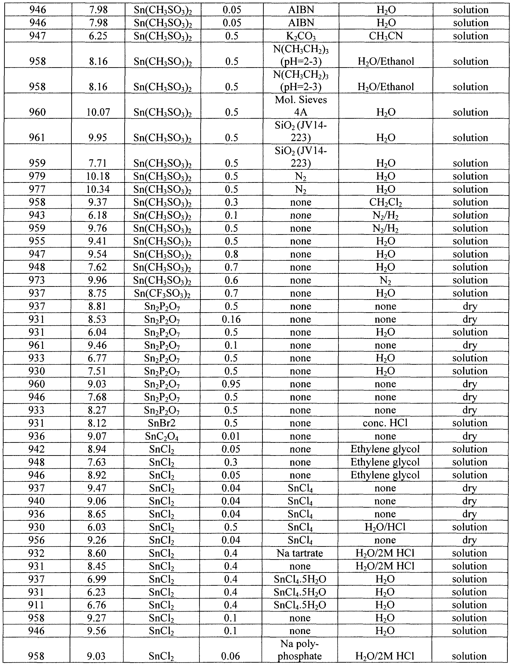


Example 15
Formation of Luminescent Material
[00108] A variety of indium halides were mixed with cesium(I) halides to form colored materials, which were then tested for photoluminescence. The indium halides included InI, InBr, InCl, InCl2, and the cesium(I) halides included CsI, CsBr, and CsCl.
Example 16
Formation and Characterization of Luminescent Material
[00109] A variety of indium halides were mixed with CsI to form colored materials, which were then tested for photoluminescence. The indium halides included InI, and a weight fraction of each indium halide with respect to a total weight was in the range of 0.01 to 0.8. The resulting materials were observed to emit light in the range of about 700 nm to about 715 nm. Heating during formation of the resulting materials was observed to increase the intensity of emitted light. In some instances, heating was performed in a nitrogen atmosphere at a temperature of about 225°C for a time period of about 2 hours.
Example 17
Formation and Characterization of Luminescent Material
[00110] A variety of silver-containing compounds, bismuth-containing compounds, copper-containing compounds, germanium-containing compounds, indium-containing compounds, tin-containing compounds, and vanadium-containing compounds were mixed with alkali halides. The resulting materials were then tested for photoluminescence using an excitation wavelength of 532 nm or an excitation wavelength in the ultraviolet range. Table 2 below sets forth ingredients and processing conditions that were used along with photoluminescent characteristics of the resulting materials. As can be appreciated with reference to Table 2, photoluminescent characteristics were observed to vary as a result of using different ingredients and processing conditions. For example, in the case of tin(II)
compounds, a peak emission wavelength was observed to correlate with a type of metal included in the alkali halides, with the order of increasing emission wavelength corresponding to potassium, rubidium, and cesium.
Table 2


Example 18
Characterization of Luminescent Material
[00111] A luminescent material was prepared by mixing a tin(II) compound with CsI, and optical characteristics of the luminescent material were measured in accordance with standard techniques.
[00112] In particular, photo luminescent characteristics were measured using an experimental setup that included a light source and a pair of spectrometers. A first one of the spectrometers was used to characterize light incident upon the luminescent material, while a second one of the spectrometers was used to characterize light emitted by the luminescent material. FIG. 4 illustrates emission spectra that were obtained for a range of excitation wavelengths. As can be appreciated with reference to FIG. 4, the luminescent material emitted light with high intensities, with a narrow spectral width of less than about 100 nm at FWHM, and with a peak emission wavelength in the range of about 930 nm to about 980 nm. Also, these photoluminescent characteristics were relatively insensitive to changes in excitation wavelength in the range of about 200 nm to about 950 nm. This insensitivity can be further appreciated with reference to FIG. 5, which illustrates an excitation spectrum of the luminescent material. Referring to FIG. 5, the excitation spectrum is substantially flat for excitation wavelengths in the range of about 200 nm to about 980 nm.
[00113] Absorption characteristics of the luminescent material were also measured in accordance with standard techniques. In particular, an absorption spectrum of the luminescent material was obtained and is superimposed onto the spectra illustrated in FIG. 4 and FIG. 5.
Example 19
Characterization of Luminescent Material
[00114] Luminescent materials were formed using a variety of ingredients and mixing techniques, and photoluminescent characteristics of those materials were measured in a similar manner as described above for Example 15. FIG. 6 illustrates emission spectra that were obtained for a subset of those materials. As can be appreciated with reference to FIG. 6, photoluminescent characteristics were readily tuned to desirable levels by adjusting ingredients and mixing techniques that were used. In particular, a peak emission wavelength was readily tuned so as to be in the range of about 910 nm to about 980 nm. FIG. 7 illustrates emission spectra that were obtained for another subset of those materials. As can be
appreciated with reference to FIG. 7, a peak emission wavelength was readily tuned so as to be in the range of about 701 nm to about 713 nm.
Example 20
Formation of Ink Composition
[00115] A melt mixture of polyethylene and docosane was prepared with a 2 to 1 weight ratio of polyethylene to docosane. Nanoparticles formed of a luminescent material were added to the melt mixture with the ratio of the nanoparticles to the melt mixture in the range of 1 part by weight per 1 ,000 parts by weight up to equal parts by weight, such as 1 part by weight of the nanoparticles per 2 parts by weight of the melt mixture. The resulting ink composition was then applied to a piece of paper using a standard coating or printing technique.
Example 21
Formation and Characterization of Luminescent Material
[00116] Luminescent materials were prepared using a vacuum deposition system. The luminescent materials were formed as films on substrates, such as 25 mm square borosilicate glass slides. In particular, reagent grade SnCl2 was placed in a first bell jar thermal evaporator boat, and reagent grade CsI was placed in a second thermal evaporator boat. Both evaporator boats were formed of tungsten. The system was evacuated to a pressure of less than Ix 10"5 torr. The thermal evaporator boat containing SnCl2 was electrically heated to yield a deposition rate of SnCl2 in the range of 0.1 nm/sec to 10 nm/sec, such as 1 nm/sec. The deposition of the SnCl2-containing layer was continued to a thickness in the range of 100 nm to 1,500 nm, such as 300 nm. After the desired thickness was obtained, the electrical current to the thermal evaporator boat containing SnCl2 was turned off, and electrical current was applied to the thermal evaporator boat containing CsI. CsI has a lower vapor pressure than SnCl2, and, accordingly, a greater amount of electrical current was applied to yield a deposition rate of CsI in the range of 0.1 nm/sec to 10 nm/sec, such as 1 nm/sec. The thickness of the Csl-containing layer was in the range of 100 nm to 1,500 nm, such as 300 nm. The thickness ratio of SnCl2 to CsI was varied in the range of 0.1 to 10. After the deposition of the layers of SnCl2 and CsI was complete, the system was vented to atmospheric conditions. The resulting materials were observed to emit light in the range of
900 nm to 1 μm, such as with a peak emission wavelength of about 930 nm or about 950 nm. In some cases, the intensity of emitted light was enhanced by annealing, such as by heating in a nitrogen purged oven for 2 minutes to 1 hour at a temperature in the range of 1200C to 35O°C. A typical annealing process involved a ramp rate of 30°C/min to 2100C for 10 minutes and a cool down at a ramp rate of 20°C/min.
Example 22
Formation and Characterization of Luminescent Material
[00117] A luminescent material was prepared using a vacuum deposition system. Reagent grade SnBr2 was placed in a first bell jar thermal evaporator boat, and reagent grade CsBr was placed in a second thermal evaporator boat. Processing conditions were similar to those described in Example 21. The resulting material was observed to emit light in the range of 700 nm to 800 nm, such as with a peak emission wavelength of about 700 nm.
Example 23
Formation and Characterization of Luminescent Material
[00118] Luminescent materials were prepared using a vacuum deposition system. Reagent grade SnBr2 was placed in a first bell jar thermal evaporator boat, and reagent grade CsI was placed in a second thermal evaporator boat. SnBr2 and CsI were then sequentially evaporated and deposited on a substrate. The deposited layers of SnBr2 and CsI were subjected to annealing for less than 20 minutes at a temperature of less than 2000C. The resulting materials were observed to emit light with a peak emission wavelength of about 700 nm. Higher annealing temperatures and longer annealing times were observed to yield materials with a peak emission wavelength of about 930 nm.
Example 24
Formation of Luminescent Material
[00119] A luminescent material was prepared using a vacuum deposition system. Reagent grade SnCl2 and reagent grade CsI were mixed, and then placed in a single bell jar thermal evaporator boat. The mixture of SnCl2 and CsI was then co-evaporated and co- deposited on a substrate to yield the luminescent material.
Example 25
Formation of Luminescent Material
[00120] A luminescent material was prepared using a vacuum deposition system. Reagent grade SnCl2 and reagent grade CsI were mixed, and then pre-melted at a temperature greater than 210°C. The pre-melted mixture was evaporated and deposited on a substrate to yield the luminescent material.
Example 26
Formation and Characterization of Luminescent Material
[00121] A luminescent material was prepared by evaporating and depositing SnCl2 and CsI. The deposition of SnCl2 and CsI was carried out with a flow of O2 gas. The flow rate of O2 gas was varied from 10 standard cubic centimeters per minute ("seem") to 200 seem. The use of O2 gas during deposition was observed to enhance the intensity and stability of the resulting photoluminescence.
Example 27
Formation and Characterization of Luminescent Material
[00122] Luminescent materials were prepared by evaporating and depositing SnCl2 and CsI. The deposition of SnCl2 and the CsI was carried out with a flow of O2 gas, and then a layer of tin metal was deposited with the flow of O2 gas continuing. The thickness of the tin metal-containing layer was in the range of 10 nm to 250 ran. The deposited layers were then annealed in a nitrogen atmosphere at a temperature in the range of 150° to 300° for 2 minutes to 1 hour. The initially metallic film became transparent or semi-transparent with various colors ranging from gold to blue to silver. The tin metal deposition was observed to enhance the intensity and stability of the resulting photoluminescence. Other materials can be deposited in place of, or in conjunction with, the tin metal, such as TiO2, SnO2, Ta2O5, BaTiO3, Pd, Ag, Au, Cu, Sn, SiN, SiO,Nj, MgO, BaSi, semiconductors, polymers, and materials used for coating and encapsulation.
Example 28 Formation of Luminescent Material
[00123] A luminescent material was prepared by evaporating and depositing SnCl2 and CsI. The deposition of SnCl2 and the CsI was carried out without a flow of O2 gas, and then a layer of tin metal was deposited with a flow of O2 gas.
Example 29
Formation of Luminescent Material
[00124] Luminescent materials were prepared using a vacuum deposition system including a thermal evaporator boat (tungsten with or without Al2O3 overcoat) and an electron-beam evaporator boat (graphite crucible). Reagent grade SnCl2 (0.25 g to 2.5 g) was placed in the thermal evaporator boat, and reagent grade CsI (0.25 g to 2.5 g) was placed in the graphite crucible for electron-beam deposition. The mass ratio of SnCl2 and CsI was varied in the range of 0.1 to 10. SnCl2 was used as a powder or a pre-melt. The pre-melt was prepared by processing SnCl2 powder at a temperature in the range of 24O0C to 26O0C for 10 minutes in a nitrogen atmosphere. CsI was used as a powder or as lcm2 pellets. The pellets were prepared with a pressure in the range of 2 x 10⁸ Pa to 3 x 10⁸ Pa using a hydraulic press. The system was evacuated to a pressure between 5 x 10"6 torr to 5 x 10"4 torr, such as less than 2 x 10"5 torr. Thermal evaporation was first carried out using an electrical current in the range of 5 A to 6 A, such as 5.5 A. Next, electron-beam deposition was carried out using an electrical current in the range of 0.5 mA to 10 mA, such as 1 mA. A high voltage setting for electron-beam deposition was in the range of 4.5 kV to 5.5 kV, such as 5.25 kV. Electron- beam sweep control was also used. A resulting rate of deposition was 0.2 nm/sec to 2 nm/sec for SnCl2 and 0.5 nm/sec to 3 nm/sec for CsI. When the deposition was complete, the system was vented with air or nitrogen, and the resulting materials were left inside the system for another 10 minutes to 15 minutes. A total thickness of 500 nm to 2,000 nm was measured using a profiling system.
Example 30
Formation of Luminescent Material
[00125] Luminescent materials were prepared using a vacuum deposition system. The thickness of a SnCl2-containing layer was in the range of 20 nm to 1 ,000 nm, and the thickness of a Csl-containing layer was in the range of 50 nm to 1,000 nm. The thickness
ratio of SnCl2 to CsI was varied in the range of 0.02 to 20. Processing conditions were similar to those described in Example 29.
Example 31
Formation of Luminescent Material
[00126] Processing conditions similar to those described in Example 29 were used to form layers of SnCl2 and CsI. Next, Al2O3 powder was placed in a graphite crucible, and then pre-melted using an electron-beam sweep with an electrical current in the range of 35 mA to 45 mA. This process was carried out for 10 minutes to 15 minutes. Then, an Al2O3 overcoat was deposited on the layers of SnCl2 and CsI using electron-beam deposition. The electron-beam deposition was carried out with an electrical current in the range of 30 mA to 40 mA and a high voltage setting of 5.25 kV, which produced a deposition rate of 0.05 nm/sec to 0.15 nm/sec. A total thickness of 50 nm to 200 nm was obtained. The Al2O3 overcoat serves to enhance the intensity and stability of the resulting photoluminescence.
Example 32
Formation of Luminescent Material
[00127] Processing conditions similar to those described in Example 29 were used to form layers of SnCl2 and CsI. Next, SiO2 crystalline chunks were placed in a graphite crucible, and SiO2 was then deposited using electron-beam deposition. The electron-beam deposition was carried out with an electrical current in the range of 8 mA to 12 mA and a high voltage setting of 5.25 kV, which produced a deposition rate of 0.5 nm/sec to 0.8 nm/sec. A total thickness of 50 nm to 200 nm was obtained. The SiO2 overcoat serves to enhance the intensity and stability of the resulting photoluminescence. Other materials can be deposited in place of, or in conjunction with, SiO2, such as TiO2, SnO2, Ta2O5, BaTiO3, Pd, Ag, Au, Cu, Sn, SiN, SiOiN,, MgO, BaSi, semiconductors, polymers, and materials used for coating and encapsulation.
Example 33
Formation of Luminescent Material
[00128] Processing conditions similar to those described in Example 29 are used, but with the order of deposition of SnCl2 and CsI reversed.
Example 34
Formation of Luminescent Material
[00129] Processing conditions similar to those described in Example 29 are used, but with multiple deposited layers of SnCl2, multiple deposited layers of CsI, or both. A typical time period between depositing each layer is from 1 minute to 2 minutes.
Example 35
Formation of Luminescent Material
[00130] Processing conditions similar to those described in Example 29 are used, but with SnCl2 and CsI being co-deposited. A typical time period between depositing each layer is from 1 minute to 2 minutes.
Example 36
Formation of Luminescent Material
[00131] Processing conditions similar to those described in Example 29 are used. After the deposition of SnCl2 and CsI is complete, the resulting material is subjected to annealing by heating in a nitrogen purged oven for 5 minutes to 2 hours at a temperature in the range of 150°C to 3500C. A typical annealing process involves a ramp rate of 5°C/min to 50°C/min.
Example 37
Formation of Luminescent Material
[00132] Luminescent materials are formed on various substrates using processing conditions similar to those described in Example 29. Examples of the substrates include silicon wafers, germanium wafers, GaAs wafers, and substrates formed of borosilicate glass, micro-roughened glass, silica, polycrystalline Al2O3, MgO, SrTiO, indium tin oxide ("ITO"), sapphire, and LiF2. The substrates have dimensions of 25 mm x 25 mm or 25 mm x 75 mm.
Example 38 Formation of Luminescent Material
[00133] Processing conditions similar to those described in Example 31 are used, but with multiple overcoat layers of Al2O3. A typical time period between depositing each overcoat layer is from 1 minute to 2 minutes.
Example 39
Formation of Luminescent Material
[00134] Processing conditions similar to those described in Example 32 are used, but with multiple overcoat layers of SiO2. A typical time period between depositing each overcoat layer is from 1 minute to 2 minutes.
Example 40
Characterization of Luminescent Material
[00135] A luminescent material including cesium, tin, and iodine was prepared, and optical characteristics of the luminescent material were measured in accordance with standard techniques. FIG. 8 illustrates an emission spectrum and an excitation spectrum that were obtained for a range of photon energies expressed in electron volts ("eV"). As can be appreciated with reference to FIG. 8, the luminescent material emitted light with high intensities, with a narrow spectral width of less than about 50 meV at FWHM, and with a peak emission wavelength of about 930 ran. Also, these photoluminescent characteristics were relatively insensitive to changes in excitation wavelength from the ultraviolet range to the emission band. These photoluminescent characteristics are unlike those of a standard CsI doped with tin, which typically emits light with shorter wavelengths, such as in the blue region or in the ultraviolet range. Absorption characteristics of the luminescent material were also measured in accordance with standard techniques. In particular, an absorption spectrum of the luminescent material was obtained and is superimposed onto the spectra illustrated in FIG. 8. As can be appreciated with reference to FIG. 8, the emission band of the luminescent material is located at or near the absorption band edge.
Example 41
Characterization of Luminescent Material
[00136] A luminescent material including cesium, tin, and bromine was prepared, and optical characteristics of the luminescent material were measured in accordance with standard
techniques. FIG. 9 illustrates an emission spectrum that was obtained for a range of photon energies. As can be appreciated with reference to FIG. 9, the luminescent material emitted light with high intensities, with a narrow spectral width, and with a peak emission wavelength of about 700 nm. These photoluminescent characteristics are unlike those of a standard CsBr doped with tin, which typically emits light with shorter wavelengths, such as in the blue region or in the ultraviolet range. Absorption characteristics of the luminescent material were also measured in accordance with standard techniques. In particular, an absorption spectrum of the luminescent material was obtained and is superimposed onto the spectrum illustrated in FIG. 9. As can be appreciated with reference to FIG. 9, the emission band of the luminescent material is located at or near the absorption band edge.
Example 42
Characterization of Luminescent Material
[00137] A luminescent material including cesium, tin, and iodine was prepared, and optical characteristics of the luminescent material were measured at different temperatures. FIG. 10 illustrates emission spectra that were obtained for a range of temperatures. As can be appreciated with reference to FIG. 10, a peak emission wavelength of the luminescent material decreased with increasing temperature. This variation of the peak emission wavelength with temperature is unlike that of many standard materials, which typically have a peak emission wavelength that increases with increasing temperature.
Example 43
Characterization of Luminescent Material
[00138] A luminescent material including cesium, lead(II), and iodine (CsPbI3) was prepared, and optical characteristics of the luminescent material were measured in accordance with standard techniques. FIG. 11 illustrates an emission spectrum that was obtained for a range of wavelengths. As can be appreciated with reference to FIG. 11 , the luminescent material emitted light with high intensities, with a narrow spectral width, and with a peak emission wavelength of about 700 nm.
Example 44 Characterization of Luminescent Material
[00139] A luminescent material including cesium, germanium(II), and iodine was prepared, and optical characteristics of the luminescent material were measured in accordance with standard techniques. FIG. 12 illustrates an emission spectrum that was obtained for a range of wavelengths. As can be appreciated with reference to FIG. 12, the luminescent material emitted light with high intensities, with a narrow spectral width, and with a peak emission wavelength of about 700 nm.
Example 45
Characterization of Luminescent Material
[00140] A luminescent material with B being a non-Group IVB element was sometimes observed to have a greater spectral width. In particular, the luminescent material including cesium, indium(I), and iodine was prepared, and optical characteristics of the luminescent material were measured in accordance with standard techniques. FIG. 13 illustrates an emission spectrum that was obtained for a range of wavelengths. As can be appreciated with reference to FIG. 13, the luminescent material emitted light with a spectral width that was greater than 100 meV. An excitation spectrum (not illustrated in FIG. 13) was observed to include a set of narrow bands within a range of excitation wavelengths.
Example 46 Formation and Characterization of Luminescent Material
[00141] Processing conditions similar to those described in Example 21 were used to prepare a luminescent material including cesium, tin, and iodine, and the luminescent material was characterized in accordance with standard X-ray Diffraction ("XRD") techniques. FIG. 14 illustrates a XRD pattern that was obtained for the luminescent material. The XRD pattern of the luminescent material was compared with XRD patterns of various standard materials, including a standard CsSnI3 (illustrated in FIG. 15A), a standard CsSnCl3 (illustrated in FIG. 15B), and a standard CsSnBr3 (illustrated in FIG. 15C), and did not produce a match. Differences in the XRD patterns indicate that the luminescent material has a different microstructure relative to the standard materials.
[00142] The luminescent material was also characterized using a microscope. The luminescent material was observed to emit light in the near infrared range, and appeared crystalline under the microscope. When illuminated with 633 nm laser light, the luminescent
material appeared bright when viewed with an infrared camera sensitive to wavelengths in the range of 850 nm to 1,000 nm.
[00143] It should be recognized that the embodiments of the invention described above are provided by way of example, and various other embodiments are encompassed by the invention. For example, while some embodiments of the invention have been described with reference to anti-counterfeiting and inventory applications, it is contemplated that the luminescent materials described herein can be used for a variety of other applications. In particular, it is contemplated that the luminescent materials can have band gap energies, electrical conductivities, and other characteristics that render the luminescent materials desirable for a variety of optoelectronic applications, such as those related to photovoltaic devices, photoconductors, photodetectors, light-emitting diodes, lasers, and other devices that involve photons and charge carriers during their operation.
[00144] For example, luminescent materials described herein can be advantageously used in photovoltaic devices as a solar down conversion material. In particular, the luminescent materials can absorb a wide range of solar wavelengths and convert the absorbed solar radiation into a peak emission wavelength. This peak emission wavelength can have an energy matched with (e.g., at or near) a band gap of a semiconductor material, such as silicon, within the photovoltaic devices. This down conversion process can increase a theoretical efficiency of a silicon photovoltaic device from 31 percent to 41 percent. Further enhancements in efficiency can occur with the use of solar down conversion concentrators, where the absorbed solar radiation from a large area is concentrated onto a small area of the semiconductor material.
[00145] A practitioner of ordinary skill in the art requires no additional explanation in developing the embodiments described herein but may nevertheless find some helpful guidance by examining the patent application of Midgley et at, U.S. Provisional Application Serial No. 60/716,656, entitled "Authenticating and Identifying Objects Using Nanoparticles" and filed on September 12, 2005, the disclosure of which is incorporated herein by reference in its entirety.
[00146] While the invention has been described with reference to the specific embodiments thereof, it should be understood by those skilled in the art that various changes may be made and equivalents may be substituted without departing from the true spirit and
scope of the invention as defined by the appended claims. In addition, many modifications may be made to adapt a particular situation, material, composition of matter, method, or process to the objective, spirit and scope of the invention. All such modifications are intended to be within the scope of the claims appended hereto. In particular, while the methods disclosed herein have been described with reference to particular operations performed in a particular order, it will be understood that these operations may be combined, sub-divided, or re-ordered to form an equivalent method without departing from the teachings of the invention. Accordingly, unless specifically indicated herein, the order and grouping of the operations are not limitations of the invention.
Claims
1. A luminescent material having the formula:  wherein
A is selected from at least one of elements of Group IA;
B is selected from at least one of elements of Group VA, elements of Group IB, elements of Group IIB, elements of Group UIB, elements of Group IVB, and elements of Group VB;
X, X', and .Y" are independently selected from at least one of elements of Group VIIB; the dopants include electron acceptors and electron donors; a is in the range of 1 to 9; b is in the range of 1 to 5; and x, x ', and x " have a sum in the range of 1 to 9; and wherein the luminescent material exhibits photoluminescence having: (a) a quantum efficiency of at least 20 percent; (b) a spectral width no greater than 100 nm at Full Width at Half Maximum; and (c) a peak emission wavelength in the near infrared range.
2. The luminescent material of claim 1, wherein B is selected from at least one of elements of Group IHB, elements of Group IVB, and elements of Group VB.
3. The luminescent material of claim 1, wherein B is selected from at least one of elements of Group IVB.
4. The luminescent material of claim 1 , wherein A is cesium, B is tin, and X, X', and X' are independently selected from at least one of chlorine, bromine, and iodine.
5. The luminescent material of claim 4, wherein the electron acceptors include cations corresponding to tin.
6. The luminescent material of claim 4, wherein the electron donors include anions corresponding to Y, and Y is selected from at least one of elements of Group VIB, elements of Group VIIB, nitrate, thiocyanate, hypochlorite, sulfate, orthophosphate, metaphosphate, oxalate, methanesulfonate, trifluoromethanesulfonate, and pyrophosphate.
7. The luminescent material of claim 1, wherein a is in the range of 1 to 5, b is in the range of 1 to 3, and the sum of x, x ', and x " is in the range of 1 to 5.
8. The luminescent material of claim 1, wherein a is 1, and the sum of x, x', and x" is 1
+ 2b.
9. The luminescent material of claim 1, wherein the quantum efficiency is at least 30 percent.
10. The luminescent material of claim 1, wherein the spectral width is no greater than 80 nm at Full Width at Half Maximum.
11. The luminescent material of claim 1 , wherein the peak emission wavelength is in the range of 700 nm to 800 nm.
12. The luminescent material of claim 1, wherein the peak emission wavelength is in the range of 900 nm to 1 μm.
13. The luminescent material of claim 1, wherein the luminescent material has a perovskite-based microstructure, and the dopants are dispersed within the perovskite-based microstructure.
14. A method of forming a luminescent material, comprising: providing a source of A and X, wherein A is selected from at least one of elements of Group IA, and X is selected from at least one of elements of Group VIIB; providing a source of B, wherein B is selected from at least one of elements of Group IHB, elements of Group IVB, and elements of Group VB; and reacting the source of A and X and the source of B to form a luminescent material having the formula: [A11BbXx], wherein a is in the range of 1 to 9, b is in the range of 1 to 5, and x is in the range of 1 to 9.
15. The method of claim 14, wherein the source of A and X is a compound having the formula: AX.
16. The method of claim 14, wherein A is cesium, and X is selected from at least one of chlorine, bromine, and iodine.
17. The method of claim 14, wherein the source of B is selected from at least one of compounds having the formulas: BY, BY2, B3Y2, B2Y, and BY4, and wherein Y is selected from at least one of elements of Group VIB, elements of Group VIIB, nitrate, thiocyanate, hypochlorite, sulfate, orthophosphate, metaphosphate, oxalate, methanesulfonate, trifiuoromethanesulfonate, and pyrophosphate.
18. The method of claim 14, wherein B is tin.
19. The method of claim 14, wherein reacting the source of A and X and the source of B includes: mixing the source of A and X and the source of B to form a mixture; and applying a pressure in the range of 1 x 10 Pascal to 7 x 10 Pascal to the mixture.
20. The method of claim 14, wherein reacting the source of A and X and the source of B includes: mixing the source of A and X and the source of B to form a mixture; and heating the mixture to a temperature in the range of 8O0C to 35O0C.
21. The method of claim 14, wherein reacting the source of A and X and the source of B includes: converting the source of A and X and the source of B into a vapor; and depositing the vapor on a substrate.
Priority Applications (4)
| Application Number | Priority Date | Filing Date | Title |
|---|---|---|---|
| ES07759029.7T ES2543717T3 (en) | 2006-03-21 | 2007-03-21 | Luminescent materials that emit light in the visible range or in the near infrared range |
| JP2009501717A JP2009530488A (en) | 2006-03-21 | 2007-03-21 | Luminescent material that emits visible or near-infrared light |
| EP07759029.7A EP2004775B1 (en) | 2006-03-21 | 2007-03-21 | Luminescent materials that emit light in the visible range or the near infrared range |
| CN200780017078.2A CN101443431B (en) | 2006-03-21 | 2007-03-21 | Luminescent materials that emit light in the visible range or the near infrared range |
Applications Claiming Priority (2)
| Application Number | Priority Date | Filing Date | Title |
|---|---|---|---|
| US78486306P | 2006-03-21 | 2006-03-21 | |
| US60/784,863 | 2006-03-21 |
Publications (3)
| Publication Number | Publication Date |
|---|---|
| WO2007109734A2 true WO2007109734A2 (en) | 2007-09-27 |
| WO2007109734A9 WO2007109734A9 (en) | 2007-11-22 |
| WO2007109734A3 WO2007109734A3 (en) | 2008-03-13 |
Family
ID=38523291
Family Applications (1)
| Application Number | Title | Priority Date | Filing Date |
|---|---|---|---|
| PCT/US2007/064534 WO2007109734A2 (en) | 2006-03-21 | 2007-03-21 | Luminescent materials that emit light in the visible range or the near infrared range |
Country Status (6)
| Country | Link |
|---|---|
| US (2) | US7641815B2 (en) |
| EP (1) | EP2004775B1 (en) |
| JP (1) | JP2009530488A (en) |
| CN (2) | CN101443431B (en) |
| ES (1) | ES2543717T3 (en) |
| WO (1) | WO2007109734A2 (en) |
Cited By (9)
| Publication number | Priority date | Publication date | Assignee | Title |
|---|---|---|---|---|
| WO2011071738A2 (en) | 2009-12-08 | 2011-06-16 | OmniPV, Inc. | Luminescent materials that emit light in the visible range or the near infrared range and methods of forming thereof |
| US8795767B2 (en) | 2006-03-21 | 2014-08-05 | OmniPV, Inc. | Luminescent materials that emit light in the visible range or the near infrared range |
| CN105185908A (en) * | 2015-08-10 | 2015-12-23 | 华南理工大学 | Solution-processed organic-inorganic planar heterojunction light emitting diode and manufacturing method thereof |
| WO2016020337A1 (en) * | 2014-08-04 | 2016-02-11 | Rhodia Operations | Modified phosphors and compositions thereof |
| WO2017020137A1 (en) | 2015-07-31 | 2017-02-09 | Nanograde Ag | Luminescent crystals and manufacturing thereof |
| JP2017142486A (en) * | 2015-11-30 | 2017-08-17 | 隆達電子股▲ふん▼有限公司 | Quantum dot composite material and manufacturing method and application thereof |
| WO2017144401A1 (en) | 2016-02-23 | 2017-08-31 | Basf Se | Luminescent particles |
| US10908318B2 (en) | 2015-06-30 | 2021-02-02 | Cambridge Enterprise Limited | Luminescent device |
| CN113398909A (en) * | 2021-06-08 | 2021-09-17 | 中国科学院物理研究所 | Perovskite material and preparation method and application thereof |
Families Citing this family (61)
| Publication number | Priority date | Publication date | Assignee | Title |
|---|---|---|---|---|
| US8974386B2 (en) | 1998-04-30 | 2015-03-10 | Abbott Diabetes Care Inc. | Analyte monitoring device and methods of use |
| GB0702092D0 (en) * | 2007-02-02 | 2007-03-14 | Fracture Code Corp Aps | Graphic Code Application Apparatus and Method |
| EP2667412A1 (en) | 2007-04-18 | 2013-11-27 | Invisage Technologies, INC. | Materials, systems and methods for optoelectronic devices |
| US20100044676A1 (en) | 2008-04-18 | 2010-02-25 | Invisage Technologies, Inc. | Photodetectors and Photovoltaics Based on Semiconductor Nanocrystals |
| US8525287B2 (en) | 2007-04-18 | 2013-09-03 | Invisage Technologies, Inc. | Materials, systems and methods for optoelectronic devices |
| US20090056791A1 (en) | 2007-06-22 | 2009-03-05 | William Matthew Pfenninger | Solar modules with enhanced efficiencies via use of spectral concentrators |
| US8203195B2 (en) | 2008-04-18 | 2012-06-19 | Invisage Technologies, Inc. | Materials, fabrication equipment, and methods for stable, sensitive photodetectors and image sensors made therefrom |
| US9042967B2 (en) | 2008-05-20 | 2015-05-26 | University Health Network | Device and method for wound imaging and monitoring |
| DE102008037442B3 (en) * | 2008-10-13 | 2010-02-25 | Thyssenkrupp Steel Ag | Method for determining changes in shape of a workpiece |
| US8822954B2 (en) * | 2008-10-23 | 2014-09-02 | Intematix Corporation | Phosphor based authentication system |
| US9496442B2 (en) * | 2009-01-22 | 2016-11-15 | Omnipv | Solar modules including spectral concentrators and related manufacturing methods |
| US8774573B2 (en) * | 2009-02-20 | 2014-07-08 | OmniPV, Inc. | Optical devices including resonant cavity structures |
| US20100236625A1 (en) * | 2009-02-20 | 2010-09-23 | John Kenney | Solar Modules Including Spectral Concentrators and Related Manufacturing Methods |
| US20100224248A1 (en) * | 2009-02-20 | 2010-09-09 | John Kenney | Solar Modules Including Spectral Concentrators and Related Manufacturing Methods |
| JP5602454B2 (en) * | 2009-09-02 | 2014-10-08 | キヤノン株式会社 | Scintillator material |
| US20110108773A1 (en) * | 2009-11-09 | 2011-05-12 | YewSavin, Inc. | Compositions for Depositions and Processing of Films for Electronic Applications |
| US8916947B2 (en) | 2010-06-08 | 2014-12-23 | Invisage Technologies, Inc. | Photodetector comprising a pinned photodiode that is formed by an optically sensitive layer and a silicon diode |
| US8840809B2 (en) * | 2011-06-01 | 2014-09-23 | Kai Shum | Solution-based synthesis of CsSnI3 thin films |
| US9196482B2 (en) * | 2011-06-01 | 2015-11-24 | Kai Shum | Solution-based synthesis of CsSnI3 |
| US20120313747A1 (en) * | 2011-06-09 | 2012-12-13 | Pawlik Thomas D | Method for authenticating security markers |
| ITRM20110361A1 (en) * | 2011-07-11 | 2013-01-12 | Matteo Repetto | PHOTOVOLTAIC DEVICE. |
| US9181475B2 (en) | 2012-02-21 | 2015-11-10 | Northwestern University | Photoluminescent compounds |
| CN103706539B (en) * | 2012-10-09 | 2015-04-29 | 浙江尚颉光电科技有限公司 | Method for using ultrasonic spray printing method to prepare cesium tin triiodide thin film |
| CN103708534B (en) * | 2012-10-09 | 2015-11-18 | 浙江尚颉光电科技有限公司 | A kind of solution method prepares the method for cesium triiodide tin thin film |
| CN103390503B (en) * | 2013-07-04 | 2016-08-10 | 华侨大学 | A kind of preparation method of sensitization solar cell solid electrolyte |
| CN103412363A (en) * | 2013-08-06 | 2013-11-27 | 西北工业大学 | Method for manufacturing polarization invisible images of near-infrared band |
| US9966726B2 (en) * | 2013-09-12 | 2018-05-08 | Nanyang Technological University | Emission source and method of forming the same |
| US9899793B2 (en) | 2013-09-12 | 2018-02-20 | Nanyang Technological University | Emission source and method of forming the same |
| US11746290B2 (en) | 2013-09-26 | 2023-09-05 | Samsung Electronics Co., Ltd. | Nanocrystal particles and processes for synthesizing the same |
| EP3058595A4 (en) * | 2013-10-16 | 2017-03-08 | Omnipv, Inc. | Photovoltaic cells including halide materials |
| US8679445B1 (en) * | 2013-11-14 | 2014-03-25 | Sun Harmonics Ltd. | Synthesis of CsSnI3 by temperature gradient solid-phase sintering method |
| US9966198B2 (en) | 2014-04-24 | 2018-05-08 | Northwestern University | Solar cells with perovskite-based light sensitization layers |
| EP2942826B1 (en) * | 2014-05-09 | 2023-03-01 | Novaled GmbH | Doped perovskites and their use as active and/or charge transport layers in optoelectronic devices |
| EP3957232A1 (en) | 2014-07-24 | 2022-02-23 | University Health Network | Collection and analysis of data for diagnostic purposes |
| TWI545178B (en) * | 2014-08-20 | 2016-08-11 | Near infrared light emitting diode and its manufacturing method | |
| US9334443B1 (en) | 2014-10-31 | 2016-05-10 | Sun Harmonics, Ltd. | Synthesis of CsSnI3 by a solution based method |
| US11205757B2 (en) | 2014-11-06 | 2021-12-21 | Sn Display Co., Ltd. | Core-shell structured perovskite particle light-emitter, method of preparing the same and light emitting device using the same |
| KR101643052B1 (en) * | 2014-11-06 | 2016-07-27 | 포항공과대학교 산학협력단 | Wavelength conversion substance, manufacturing method of the same and light-emitting device comprising the same |
| KR101724210B1 (en) | 2014-11-06 | 2017-04-07 | 포항공과대학교 산학협력단 | Perovskite light emitting element for the light emitting layer and a method of manufacturing and using the same Perovskite light emitting element |
| WO2016072810A1 (en) | 2014-11-06 | 2016-05-12 | 포항공과대학교 산학협력단 | Perovskite light emitting device containing exciton buffer layer and method for manufacturing same |
| GB201421133D0 (en) * | 2014-11-28 | 2015-01-14 | Cambridge Entpr Ltd | Electroluminescent device |
| GB201501342D0 (en) * | 2015-01-27 | 2015-03-11 | Univ Lancaster | Improvements relating to the authentication of physical entities |
| EP3168278B2 (en) | 2015-10-28 | 2022-02-09 | Samsung Electronics Co., Ltd. | Quantum dots, production methods thereof, and electronic devices including the same |
| TWI598429B (en) * | 2015-11-30 | 2017-09-11 | 隆達電子股份有限公司 | Wavelength-converting material and application thereof |
| KR102498798B1 (en) | 2015-12-22 | 2023-02-09 | 삼성전자주식회사 | Quantum dots and devices including the same |
| US10775671B2 (en) * | 2015-12-23 | 2020-09-15 | Avantama Ag | Display device |
| US10585228B2 (en) | 2015-12-29 | 2020-03-10 | Samsung Electronics Co., Ltd. | Quantum dots, production methods thereof, and electronic devices including the same |
| US10340844B2 (en) * | 2016-05-05 | 2019-07-02 | Washington State University | High-performance planar solar concentrators based on nanoparticle doping |
| CN105895726A (en) * | 2016-05-11 | 2016-08-24 | 徐翔星 | Solar cell containing perovskite nano crystal down-conversion layer and preparation method thereof |
| WO2017210266A1 (en) | 2016-05-31 | 2017-12-07 | Alliance For Sustainable Energy, Llc | Nanoparticles for photovoltaic and led devices and methods of making the same |
| US10544168B2 (en) | 2016-06-15 | 2020-01-28 | Alliance For Sustainable Energy, Llc | Ligand-exchangeable nanoparticles and methods of making the same |
| US11702762B2 (en) | 2016-08-11 | 2023-07-18 | Avantama Ag | Luminescent crystals and manufacturing thereof |
| JP2018529793A (en) * | 2016-08-11 | 2018-10-11 | アファンタマ アクチェンゲゼルシャフト | Luminescent crystals and their production |
| EP3282000A1 (en) * | 2016-08-11 | 2018-02-14 | Avantama AG | Solid polymer composition |
| CN106433641B (en) * | 2016-09-05 | 2018-08-21 | 中南大学 | A kind of method that low heat temperature solid state reaction prepares rear-earth-doped calcium stannate fluorescent material |
| CN106634961B (en) * | 2016-12-19 | 2019-02-19 | 中央民族大学 | A kind of organic inorganic hybridization perovskite quantum dot and preparation method thereof |
| US10553367B2 (en) * | 2017-10-20 | 2020-02-04 | Qatar Foundation | Photovoltaic perovskite oxychalcogenide material and optoelectronic devices including the same |
| CN112680211A (en) | 2019-10-17 | 2021-04-20 | 三星电子株式会社 | Core-shell quantum dot, method for producing same, quantum dot group, quantum dot composite, quantum dot composition, and display device |
| EP3809480A1 (en) * | 2019-10-17 | 2021-04-21 | Samsung Electronics Co., Ltd. | Core shell quantum dot, production method thereof, and electronic device including the same |
| CN111470528A (en) * | 2020-04-11 | 2020-07-31 | 上海科技大学 | Tin-containing semiconductor material and preparation method thereof |
| CN112647047B (en) * | 2020-12-02 | 2022-02-15 | 河南大学 | Preparation method and application of cesium tin iodine film |
Family Cites Families (39)
| Publication number | Priority date | Publication date | Assignee | Title |
|---|---|---|---|---|
| US2196077A (en) * | 1937-06-25 | 1940-04-02 | Aluminum Co Of America | Method of producing sodium aluminum fluoride |
| US3655332A (en) * | 1970-06-15 | 1972-04-11 | Foote Mineral Co | PROCESS FOR PREPARING LITHIUM COMPOUNDS OF THE FORMULA LiMF{11 {0 WHEREIN M IS ARSENIC OR ANTIMONY |
| US4076794A (en) * | 1974-08-01 | 1978-02-28 | Foote Mineral Company | Process for the production of high purity alkali metal tetrahaloaluminates and products produced thereby |
| US4054645A (en) * | 1976-08-24 | 1977-10-18 | Minnesota Mining And Manufacturing Company | Radiodiagnostic complexes employing fluorine-containing tin reducing agents |
| DE2952436A1 (en) * | 1979-12-27 | 1981-07-02 | Karl Dr.rer.nat. 4300 Essen Heidrich | Light-emitting layer of plumbate cpd. - with octahedral halogen coordination of lead giving any desired colour, e.g. for fluorescent lamp or phosphor screen |
| DE3578359D1 (en) * | 1984-12-17 | 1990-07-26 | Konishiroku Photo Ind | SCREEN FOR SAVING A RADIATION IMAGE. |
| FR2586508B1 (en) * | 1985-08-23 | 1988-08-26 | Thomson Csf | RADIOLOGICAL IMAGE ENHANCER TUBE ENTRY SCREEN SCINTILLER AND METHOD FOR MANUFACTURING SUCH A SCINTILLATOR |
| US4835711A (en) * | 1986-05-30 | 1989-05-30 | Zymark Corporation | Quickly reconfigurable robotic system |
| US5366896A (en) * | 1991-07-30 | 1994-11-22 | University Of Virginia Alumni Patents Foundation | Robotically operated laboratory system |
| WO1994008759A1 (en) * | 1992-10-16 | 1994-04-28 | Thomas Jefferson University | Method and apparatus for robotically performing sanger dideoxynucleotide dna sequencing reactions |
| US5318764A (en) * | 1992-11-09 | 1994-06-07 | Advance Research Chemicals, Inc. | Processes of producing potassium fluoroaluminates |
| DE69529700T2 (en) * | 1994-06-03 | 2003-10-16 | Agfa-Gevaert, Mortsel | New class of high-energy detection materials |
| JPH08102293A (en) | 1994-09-29 | 1996-04-16 | Toshiba Lighting & Technol Corp | High-pressure discharge lamp, high-pressure discharge lamp lighting device, and lighting system |
| EP0751200B1 (en) * | 1995-06-30 | 1999-03-03 | Agfa-Gevaert N.V. | A radiation image storage screen comprising an alkali metal halide phosphor |
| DE69601603T2 (en) * | 1995-06-30 | 1999-09-23 | Agfa-Gevaert N.V., Mortsel | Screen for storing a radiation image with alkali halide phosphor |
| US6652967B2 (en) * | 2001-08-08 | 2003-11-25 | Nanoproducts Corporation | Nano-dispersed powders and methods for their manufacture |
| US5721634A (en) * | 1996-10-09 | 1998-02-24 | Boeing North American, Inc. | Cesium-germanium halide salts forming nonlinear optical crystals |
| US5985214A (en) * | 1997-05-16 | 1999-11-16 | Aurora Biosciences Corporation | Systems and methods for rapidly identifying useful chemicals in liquid samples |
| EP1113458B1 (en) * | 1999-12-27 | 2005-02-02 | Agfa-Gevaert | A binderless storage phosphor screen with needle shaped crystals and methods for producing the same |
| DE10015486A1 (en) * | 2000-03-30 | 2001-10-11 | Solvay Fluor & Derivate | Flux containing alkali fluorostannate, preferably potassium and/or cesium fluorostannate and mixture of potassium and cesium fluorostannate is used for soldering and brazing aluminum (alloy) parts |
| EP1217633B1 (en) * | 2000-12-22 | 2007-05-30 | Agfa HealthCare NV | A cesium bromide storage phosphor with narrow emission spectrum upon UV-excitation |
| US6730243B2 (en) * | 2000-12-22 | 2004-05-04 | Afga-Gevaert | Cesium halide storage phosphor with narrow emission spectrum upon UV-excitation |
| JP2003028994A (en) * | 2001-07-10 | 2003-01-29 | Fuji Photo Film Co Ltd | Radiation image conversion panel and production method therefor |
| JP2003050298A (en) * | 2001-08-06 | 2003-02-21 | Fuji Photo Film Co Ltd | Radiographic image conversion panel and its manufacturing method |
| DE10148161A1 (en) * | 2001-09-28 | 2003-04-24 | Siemens Ag | Luminescent material, used in production of X-ray amplifier plate, is made from alkali halide |
| JP3933591B2 (en) * | 2002-03-26 | 2007-06-20 | 淳二 城戸 | Organic electroluminescent device |
| US7464185B2 (en) * | 2002-04-30 | 2008-12-09 | Hewlett-Packard Development Company, L.P. | Method and apparatus for transfering data from a sending system to a receiving system, and program storage devices |
| JP2004122642A (en) * | 2002-10-03 | 2004-04-22 | Konica Minolta Holdings Inc | Method for creating identification card for certification and transfer foil for protecting surface of card used for this method |
| US20050107870A1 (en) * | 2003-04-08 | 2005-05-19 | Xingwu Wang | Medical device with multiple coating layers |
| US7351442B2 (en) * | 2003-12-19 | 2008-04-01 | Agfa-Gevaert | Method of preparing storage phosphors from dedicated precursors |
| US7141794B2 (en) * | 2004-06-28 | 2006-11-28 | General Electric Company | Scintillator compositions, related processes, and articles of manufacture |
| US7648649B2 (en) * | 2005-02-02 | 2010-01-19 | Lumination Llc | Red line emitting phosphors for use in led applications |
| US7497973B2 (en) * | 2005-02-02 | 2009-03-03 | Lumination Llc | Red line emitting phosphor materials for use in LED applications |
| WO2007109690A2 (en) * | 2006-03-21 | 2007-09-27 | Ultradots, Inc. | Authenticating and identifying objects by detecting markings through turbid materials |
| WO2007109734A2 (en) | 2006-03-21 | 2007-09-27 | Ultradots, Inc. | Luminescent materials that emit light in the visible range or the near infrared range |
| EP2510073B1 (en) * | 2009-12-08 | 2017-07-05 | Omnipv, Inc. | Luminescent materials that emit light in the visible range or the near infrared range and methods of forming thereof |
| US8840809B2 (en) * | 2011-06-01 | 2014-09-23 | Kai Shum | Solution-based synthesis of CsSnI3 thin films |
| US8529797B2 (en) * | 2011-06-01 | 2013-09-10 | Kai Shum | Perovskite semiconductor thin film and method of making thereof |
| US9181475B2 (en) * | 2012-02-21 | 2015-11-10 | Northwestern University | Photoluminescent compounds |
-
2007
- 2007-03-21 WO PCT/US2007/064534 patent/WO2007109734A2/en active Application Filing
- 2007-03-21 CN CN200780017078.2A patent/CN101443431B/en not_active Expired - Fee Related
- 2007-03-21 CN CN201310145214.3A patent/CN103254896B/en not_active Expired - Fee Related
- 2007-03-21 US US11/689,381 patent/US7641815B2/en not_active Expired - Fee Related
- 2007-03-21 JP JP2009501717A patent/JP2009530488A/en active Pending
- 2007-03-21 ES ES07759029.7T patent/ES2543717T3/en active Active
- 2007-03-21 EP EP07759029.7A patent/EP2004775B1/en not_active Not-in-force
-
2009
- 2009-11-02 US US12/611,062 patent/US8795767B2/en not_active Expired - Fee Related
Cited By (20)
| Publication number | Priority date | Publication date | Assignee | Title |
|---|---|---|---|---|
| US8734681B2 (en) | 2006-03-21 | 2014-05-27 | OmniPV, Inc. | Luminescent materials that emit light in the visible range or the near infrared range and methods of forming thereof |
| US8795767B2 (en) | 2006-03-21 | 2014-08-05 | OmniPV, Inc. | Luminescent materials that emit light in the visible range or the near infrared range |
| US9660111B2 (en) | 2006-03-21 | 2017-05-23 | OmniPV, Inc. | Luminescent materials that emit light in the visible range or the near infrared range and methods of forming thereof |
| EP2510073A2 (en) * | 2009-12-08 | 2012-10-17 | Omnipv, Inc. | Luminescent materials that emit light in the visible range or the near infrared range and methods of forming thereof |
| EP2510073A4 (en) * | 2009-12-08 | 2014-09-24 | Omnipv Inc | Luminescent materials that emit light in the visible range or the near infrared range and methods of forming thereof |
| WO2011071738A2 (en) | 2009-12-08 | 2011-06-16 | OmniPV, Inc. | Luminescent materials that emit light in the visible range or the near infrared range and methods of forming thereof |
| WO2016020337A1 (en) * | 2014-08-04 | 2016-02-11 | Rhodia Operations | Modified phosphors and compositions thereof |
| US10908318B2 (en) | 2015-06-30 | 2021-02-02 | Cambridge Enterprise Limited | Luminescent device |
| WO2017020137A1 (en) | 2015-07-31 | 2017-02-09 | Nanograde Ag | Luminescent crystals and manufacturing thereof |
| US11414597B2 (en) | 2015-07-31 | 2022-08-16 | Avantama Ag | Luminescent crystals and manufacturing thereof |
| US11286421B2 (en) | 2015-07-31 | 2022-03-29 | Avantama Ag | Luminescent crystals and manufacturing thereof |
| US10920137B2 (en) | 2015-07-31 | 2021-02-16 | Avantama Ag | Luminescent crystals and manufacturing thereof |
| CN105185908A (en) * | 2015-08-10 | 2015-12-23 | 华南理工大学 | Solution-processed organic-inorganic planar heterojunction light emitting diode and manufacturing method thereof |
| US10816716B2 (en) | 2015-11-30 | 2020-10-27 | Lextar Electronics Corporation | Application of quantum dot composite material |
| US10436973B2 (en) | 2015-11-30 | 2019-10-08 | Lextar Electronics Corporation | Quantum dot composite material and manufacturing method and application thereof |
| EP3192846A3 (en) * | 2015-11-30 | 2017-11-29 | Lextar Electronics Corp. | Quantum dot composite material and manufacturing method and application thereof |
| JP2017142486A (en) * | 2015-11-30 | 2017-08-17 | 隆達電子股▲ふん▼有限公司 | Quantum dot composite material and manufacturing method and application thereof |
| WO2017144401A1 (en) | 2016-02-23 | 2017-08-31 | Basf Se | Luminescent particles |
| CN113398909A (en) * | 2021-06-08 | 2021-09-17 | 中国科学院物理研究所 | Perovskite material and preparation method and application thereof |
| CN113398909B (en) * | 2021-06-08 | 2022-05-24 | 中国科学院物理研究所 | Perovskite material and preparation method and application thereof |
Also Published As
| Publication number | Publication date |
|---|---|
| EP2004775A2 (en) | 2008-12-24 |
| EP2004775A4 (en) | 2010-04-21 |
| US20080014463A1 (en) | 2008-01-17 |
| US8795767B2 (en) | 2014-08-05 |
| WO2007109734A3 (en) | 2008-03-13 |
| EP2004775B1 (en) | 2015-05-06 |
| US7641815B2 (en) | 2010-01-05 |
| US20100055350A1 (en) | 2010-03-04 |
| CN101443431B (en) | 2014-05-21 |
| CN103254896B (en) | 2015-01-21 |
| CN101443431A (en) | 2009-05-27 |
| WO2007109734A9 (en) | 2007-11-22 |
| JP2009530488A (en) | 2009-08-27 |
| ES2543717T3 (en) | 2015-08-21 |
| CN103254896A (en) | 2013-08-21 |
Similar Documents
| Publication | Publication Date | Title |
|---|---|---|
| US7641815B2 (en) | Luminescent materials that emit light in the visible range or the near infrared range | |
| Zhang et al. | Dual‐band‐tunable white‐light emission from Bi3+/Te4+ emitters in perovskite‐derivative Cs2SnCl6 microcrystals | |
| Li et al. | High Br–content CsPb (Cl y Br1–y) 3 perovskite nanocrystals with strong Mn2+ emission through diverse cation/anion exchange engineering | |
| Kumar et al. | Composition‐Dependent Photoluminescence Properties and Anti‐Counterfeiting Applications of A2AgX3 (A= Rb, Cs; X= Cl, Br, I) | |
| Liu et al. | Suppression of temperature quenching in perovskite nanocrystals for efficient and thermally stable light-emitting diodes | |
| Zhang et al. | Conversion of invisible metal-organic frameworks to luminescent perovskite nanocrystals for confidential information encryption and decryption | |
| Liu et al. | Facile single‐precursor synthesis and surface modification of hafnium oxide nanoparticles for nanocomposite γ‐ray scintillators | |
| González‐Carrero et al. | Organometal halide perovskites: bulk low‐dimension materials and nanoparticles | |
| US20080138604A1 (en) | Authenticating and identifying objects using markings formed with correlated random patterns | |
| US20080038494A1 (en) | Authenticating and identifying objects by detecting markings through turbid materials | |
| US8785866B2 (en) | Compositions having multiple responses to excitation radiation and methods for making same | |
| Ge et al. | Realizing Color‐Tunable and Time‐Dependent Ultralong Afterglow Emission in Antimony‐Doped CsCdCl3 Metal Halide for Advanced Anti‐Counterfeiting and Information Encryption | |
| Baek et al. | Mechanochemistry-driven engineering of 0D/3D heterostructure for designing highly luminescent Cs–Pb–Br perovskites | |
| KR101967029B1 (en) | Perovskite luminous structure and method of manufacturing the perovskite luminous structure | |
| Mesaros et al. | A valence states approach for luminescence enhancement by low dopant concentration in Eu-doped ZnO nanoparticles | |
| Zhang et al. | Direct Photolithographic Deposition of Color‐Coded Anti‐Counterfeit Patterns with Titania Encapsulated Upconverting Nanoparticles | |
| Zhang et al. | Highly bright and stable white-light-emitting cadmium-free Ag, Mn co-doped Zn–In–S/ZnS quantum dots and their electroluminescence | |
| Grandhi et al. | Strategies for improving luminescence efficiencies of blue-emitting metal halide perovskites | |
| Dhania et al. | Synthesis, characterization and photoluminescent properties of Eu (III) complexes with 5-hydroxy-2-hydroxymethyl-4H-4-pyranone and N, N′-donor heterocyclic coligands | |
| Kim et al. | Phosphorescent energy downshifting for diminishing surface recombination in silicon nanowire solar cells | |
| Gangwar et al. | New insight into printable europium-doped yttrium borate luminescent pigment for security ink applications | |
| Erdem et al. | Sweet plasmonics: Sucrose macrocrystals of metal nanoparticles | |
| Akhtar et al. | Morphology‐Tailored Synthesis of PbSe Nanocrystals and Thin Films from Bis [N, N‐diisobutyl‐N′‐(4‐nitrobenzoyl) selenoureato] lead (II) | |
| Sharma et al. | Synthesis of Er doped ZnO cone-like nanostructures with enhanced structural, optical and magnetic properties | |
| Mandal et al. | Optical performance of europium-doped β gallium oxide PVD thin films |
Legal Events
| Date | Code | Title | Description |
|---|---|---|---|
| 121 | Ep: the epo has been informed by wipo that ep was designated in this application |
Ref document number: 07759029 Country of ref document: EP Kind code of ref document: A2 |
|
| WWE | Wipo information: entry into national phase |
Ref document number: 2009501717 Country of ref document: JP |
|
| NENP | Non-entry into the national phase |
Ref country code: DE |
|
| WWE | Wipo information: entry into national phase |
Ref document number: 2007759029 Country of ref document: EP |
|
| WWE | Wipo information: entry into national phase |
Ref document number: 200780017078.2 Country of ref document: CN |