US8713417B2 - Multi-channel memory system including error correction decoder architecture with efficient area utilization - Google Patents
Multi-channel memory system including error correction decoder architecture with efficient area utilization Download PDFInfo
- Publication number
- US8713417B2 US8713417B2 US12/198,992 US19899208A US8713417B2 US 8713417 B2 US8713417 B2 US 8713417B2 US 19899208 A US19899208 A US 19899208A US 8713417 B2 US8713417 B2 US 8713417B2
- Authority
- US
- United States
- Prior art keywords
- error
- data set
- errors
- data
- communication channel
- Prior art date
- Legal status (The legal status is an assumption and is not a legal conclusion. Google has not performed a legal analysis and makes no representation as to the accuracy of the status listed.)
- Active, expires
Links
Images


Classifications
-
- G—PHYSICS
- G06—COMPUTING OR CALCULATING; COUNTING
- G06F—ELECTRIC DIGITAL DATA PROCESSING
- G06F11/00—Error detection; Error correction; Monitoring
- G06F11/07—Responding to the occurrence of a fault, e.g. fault tolerance
- G06F11/08—Error detection or correction by redundancy in data representation, e.g. by using checking codes
- G06F11/10—Adding special bits or symbols to the coded information, e.g. parity check, casting out 9's or 11's
- G06F11/1008—Adding special bits or symbols to the coded information, e.g. parity check, casting out 9's or 11's in individual solid state devices
- G06F11/1068—Adding special bits or symbols to the coded information, e.g. parity check, casting out 9's or 11's in individual solid state devices in sector programmable memories, e.g. flash disk
-
- G—PHYSICS
- G11—INFORMATION STORAGE
- G11C—STATIC STORES
- G11C29/00—Checking stores for correct operation ; Subsequent repair; Testing stores during standby or offline operation
- G11C29/04—Detection or location of defective memory elements, e.g. cell constructio details, timing of test signals
- G11C29/08—Functional testing, e.g. testing during refresh, power-on self testing [POST] or distributed testing
- G11C29/12—Built-in arrangements for testing, e.g. built-in self testing [BIST] or interconnection details
- G11C29/38—Response verification devices
- G11C29/42—Response verification devices using error correcting codes [ECC] or parity check
Definitions
- This invention pertains to the field of memory systems, and more particularly, to the field of memory systems employing error correction decoding.
- a multi-channel error correction coder (ECC) architecture is employed with buffer memories for encoding/decoding the data from the host system to and from the flash memory.
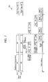
- FIG. 1 shows a block diagram of such a flash memory system 10 .
- Flash memory system 10 includes a flash memory controller 100 and a memory block 200 .
- Memory controller 100 includes a host interface 190 , a user data buffer 120 , a system data buffer 130 , a NAND interface 140 , and a central processing unit 150 , all connected together by a system bus 160 .
- NAND interface 140 includes a direct memory access (DMA) controller 144 and an error correction coder (ECC) block 145 .
- ECC block 145 includes a plurality (N) of ECC modules, including ECC modules 141 , 142 and 143 .
- Memory block 200 includes a plurality (N) of NAND memory devices, including memory devices 211 , 212 and 213 .
- NAND interface 140 may include a plurality (M) of direct memory access (DMA) controller 144 .
- M is integer greater than 1.
- M may be same as N or not.
- FIG. 2 illustrates in greater detail interconnections between ECC block 145 and memory devices 211 , 212 and 213 in flash memory system 10 .
- ECC module 141 includes encoder 161 , and decoder block 165 , which further comprises detector 162 and corrector 163 .
- ECC module 142 includes encoder 171 , and decoder block 175 , which further comprises detector 172 and corrector 173 ; and
- ECC module 143 includes encoder 181 , and decoder block 185 , which further comprises detector 182 and corrector 183 .
- data from a host device e.g., a processor
- a host device e.g., a processor
- ECC module 141 the data is first encoded by the encoder 161 and then transmitted to memory device 211 via channel 0 .
- decoder 165 When data is to be read from memory device 211 and provided to a host device, it is first decoded by decoder 165 and then the decoded data is supplied to DMA controller 144 .
- decoder 165 detector 162 detects whether any errors are present in the data received from memory device 211 , and if there are any errors, then corrector 163 corrects the errors.
- flash memory systems There is a trend for flash memory systems to have more and more memory devices. There is also a trend for flash memory systems to employ multi-level cell (MLC) NAND memory devices for increased storage capacity. As a result, flash memory systems also require more and more ECC modules. However, adding more ECC modules enlarges the size of the integrated circuit, and increases the number of ECC IP core gates, for the flash memory controller. This increases the complexity and cost of the flash memory system.
- MLC multi-level cell
- the present invention is directed to a memory system, and a method of processing data in a memory system.
- a memory system comprises: at least two memory devices; and a memory controller having at least first and second communication channels each for communicating data with at least one of the memory devices.
- the memory controller comprises: at least first and second error detectors corresponding to the first and second communication channels and each adapted to detect errors in data sets received via the corresponding communication channel from at least one of the memory devices; and an error corrector adapted to correct errors detected by each of the at least first and second error detectors.
- a memory system comprises: a memory controller having a first input port for communication with a first memory device via a first communication channel, a second input port for communication with a second memory device via a second communication channel, and an error decoder that is multiplexed for decoding data received from both the first and the second communication channels.
- a method of processing data received from at least two memory devices via at least two corresponding communication channels comprises: detecting errors in a first data set received via a first communication channel while detecting errors in a second data set received via a second communication channel; and correcting the detected errors in the first data set and then subsequently correcting errors in the second data set.
- an error decoder comprises: at least first and second error detectors corresponding to first and second communication channels and each adapted to detect errors in data sets received via the corresponding communication channel from at least one of memory devices; and an error corrector adapted to correct errors detected by each of the at least first and second error detectors
- FIG. 1 shows a block diagram of a flash memory system.
- FIG. 2 illustrates connections between an error correction coder (ECC) block and memory devices.
- ECC error correction coder
- FIG. 3 illustrates a block diagram of one embodiment of a flash memory error correction coder (ECC) block that can operate in a two channel memory system.
- ECC flash memory error correction coder
- FIG. 4 illustrates a block diagram of another embodiment of a flash memory error correction coder (ECC) block that can operate in a two channel memory system.
- ECC flash memory error correction coder
- FIG. 5 illustrates a block diagram of one embodiment of a flash memory error correction decoder that can operate in a pipelined mode.
- FIG. 6 illustrates a two channel flash memory system that can operate in a pipelined mode with a buffer memory structure.
- FIG. 7 illustrates a timing chart of pipelined decoding operations of a Bose-Chaudhuri-Hocquenghem (BCH) flash memory error correction decoder.
- BCH Bose-Chaudhuri-Hocquenghem
- FIG. 3 illustrates a block diagram of one embodiment of a flash memory error correction coder (ECC) block 300 that can operate in a two channel memory system.
- ECC block 300 is a Bose-Chaudhuri-Hocquenghem (BCH) error correction coder.
- BCH Bose-Chaudhuri-Hocquenghem
- ECC block 300 includes two data encoders 361 , one each for the first and second communication channels.
- ECC block 300 also includes two syndrome computation blocks 310 a and 310 b , again one for each of the first and second communication channels.
- ECC block 300 further includes a multiplexer (or data switch) 315 , a key equation solver (KES) block 320 , Chien search and error evaluator blocks 330 and 335 , and a decoder controller 340 .
- KES key equation solver
- ECC block 300 communicates data with memory devices (e.g., flash memory devices) over two communication channels operating at the same time as each other in parallel.
- memory devices e.g., flash memory devices
- the data is first encoded (e.g. with a BCH code) by a corresponding encoder 361 for each communication channel. Then, the encoded data is transmitted in parallel across the two communication channels to the memory devices.
- syndrome computation block 310 a computes the syndrome of a first set of data (e.g., data from an Nth sector of memory) received via the first communication channel at the same time that syndrome computation block 310 b computes the syndrome of a second set of data (e.g., data from an Mth sector of memory) via the second communication channel.
- first set of data e.g., data from an Nth sector of memory
- second set of data e.g., data from an Mth sector of memory
- the syndrome computation blocks 310 a and 310 b detect whether or not a data set includes errors.
- ECC block 300 includes multiplexer 315 so that the two communication channels can share one key equation solver (KES) block 320 , and one Chien search and error evaluator (blocks 330 and 335 ), under control of controller 340 . That is, multiplexer 315 multiplexes between the first and second communication channels for locating errors that occur in data sets received from the memory devices via the communication channels. Once the errors are identified in a data set, then the errors are corrected in a further error correction block not shown in FIG. 3 (e.g., an exclusive-or (XOR) circuit) and the decoded data set may then be sent to a host device (e.g., a processor).
- a host device e.g., a processor
- FIG. 4 illustrates a block diagram of another embodiment of a flash memory error correction coder (ECC) block 400 that can operate in a two-channel memory system.
- ECC block 400 is a convolutional error correction coder.
- ECC block 400 includes a Viterbi decoder.
- ECC block 400 includes two data encoders 461 , one each for the first and second communication channels.
- ECC block 400 also includes two branch matrix calculators 410 a and 410 b , again one for each of the first and second communication channels.
- ECC block 400 further includes a multiplexer (or data switch) 415 , add-compare-select (ACS) block 420 , state metrics memory (SMM) 430 , and survivor path memory (SPM) 435 .
- ACS add-compare-select
- SMM state metrics memory
- SPM survivor path memory
- ECC block 400 communicates data with memory devices (e.g., flash memory devices) over two communication channels operating at the same time as each other in parallel.
- memory devices e.g., flash memory devices
- the data is first encoded (e.g., convolutionally encoded) by a corresponding encoder 461 for each communication channel. Then, the encoded data is transmitted in parallel across the two communication channels to the memory devices.
- branch matrix calculator 410 a calculates the branch metrics of each trellis branch for a first set of data (e.g., data from an Nth sector of memory) received via the first communication channel at the same time that branch matrix calculator 410 b calculates the branch metrics of each trellis branch for a second set of data (e.g., data from an Mth sector of memory) via the second communication channel.
- a first set of data e.g., data from an Nth sector of memory
- branch matrix calculator 410 b calculates the branch metrics of each trellis branch for a second set of data (e.g., data from an Mth sector of memory) via the second communication channel.
- ECC block 400 includes multiplexer 415 so that the two communication channels can share one add-compare-select (ACS) block 420 , one state metrics memory (SMM) 430 , and one survivor path memory (SPM) 435 . That is, multiplexer 415 multiplexes between the first and second communication channels for correcting errors that occur in data sets received from the memory devices via the communication channels.
- ACS add-compare-select
- SMM state metrics memory
- SPM survivor path memory
- FIG. 5 illustrates a block diagram of one embodiment of a BCH flash memory error correction decoder 500 that can operate in a pipelined mode.
- Decoder 500 includes a syndrome computation block 510 , a key equation solver (KES) block 520 , a Chien search and error evaluator (CSEE) block 530 , a decoder controller 540 , a demultiplexer (or data switch) 555 , an error corrector 563 , a first buffer memory 570 , a second buffer memory 580 , and a multiplexer (or data switch) 590 .
- KES key equation solver
- CSEE Chien search and error evaluator
- a first set of data (e.g., data from Nth sector) is received via demultiplexer 555 into first buffer memory 570 and syndrome computation block 510 computes a syndrome of a first set of data. If the syndrome indicates that errors have occurred in the first data set, decoder controller 540 controls KES block 520 and Chien search and error evaluator block 530 to locate the errors in the first set of data while attempting to minimize latency delays to error corrector 563 . Multiplexer 590 sends the first set of data from first memory buffer 570 to error corrector 563 for error correction.
- a second set of data (e.g., data from an (N+1)th sector) is received via demultiplexer 550 into second buffer memory 580 and syndrome computation block 510 computes a syndrome of the second set of data.
- the decoder controller 540 controls (KES) block 520 and Chien search and error evaluator block 530 to locate the errors in the second set of data, wherein multiplexer 590 sends the second set of data from second memory buffer 580 to error corrector 563 for error correction.
- a third set of data may be received via demultiplexer 550 into first buffer memory 570 and syndrome computation block 510 computes a syndrome of a third set of data.
- the process continues in like manner for all subsequent sets of data (e.g., sectors from a memory device).
- FIG. 6 illustrates a two channel flash memory system 60 that can operate in a pipelined mode with a buffer memory structure.
- Flash memory system 60 includes a flash memory controller 600 and NAND memory devices 611 and 612 .
- Flash memory controller 600 communicates data with memory devices 611 and 612 over two communication channels operating at the same time as each other in parallel.
- Flash memory controller 600 includes ECC block 645 and host interface 690 .
- ECC block 645 includes two data encoders 661 , one each for the first and second communication channels.
- ECC block 645 also includes two syndrome computation blocks 610 a and 610 b , again one for each of the first and second communication channels.
- ECC block 645 further includes a multiplexer (or data switch) 615 , a decoder block 630 , a demultiplexer 675 , first and second memory buffers 670 and 680 , third and fourth memory buffers (not labeled), and an error correction block 663 .
- ECC block 645 communicates data with memory devices 611 and 612 over two communication channels operating at the same time as each other in parallel.
- a host device e.g., a processor
- the data is first encoded (e.g. with a BCH code) by a corresponding encoder 661 for each communication channel. Then, the encoded data is transmitted in parallel across the two communication channels to memory devices 611 and 612 .
- syndrome computation block 610 a computes the syndrome of a first set of data (e.g., data from an Nth sector of memory) received via the first communication channel at the same time that syndrome computation block 610 b computes the syndrome of a second set of data (e.g., data from an Mth sector of memory) via the second communication channel.
- first set of data e.g., data from an Nth sector of memory
- second set of data e.g., data from an Mth sector of memory
- the syndrome computation blocks 610 a and 610 b detect whether or not a data set includes errors.
- ECC block 645 includes multiplexer 615 so that the two communication channels can share one key equation solver (error decoder block 630 . That is, multiplexer 615 multiplexes between the first and second communication channels for locating errors that occur in data sets received from the memory devices via the communication channels. Once the errors are identified in a data set, then the errors are corrected in error correction block 663 (e.g., an exclusive-or (XOR) circuit) and the decoded data set may then be sent to a host device (e.g., a processor).
- error correction block 663 e.g., an exclusive-or (XOR) circuit
- ECC block 645 operates in a pipeline mode as follows. When data sets are read into memory controller 600 from the two memory chips 611 and 612 , errors in the data sets received from the two communication channels are detected at the same time. At this time, the data sets are stored in buffer memories 670 and 680 , waiting for correction and transmission to the host.
- Decoder block 630 calculates the error locations for a first data set read data from memory device 611 , and then the first set of data stored in buffer memory 670 is corrected and transmitted to the host. While the first data set stored in buffer memory 670 is being transmitted to the host, decoder block 630 calculates error locations for a second data set read data from memory device 612 , and then the second set of data stored in buffer memory 680 is corrected and transmitted to the host after the data in the buffer memory 670 has finished.
- FIG. 7 illustrates a timing chart 700 of pipelined decoding operations for a BCH flash memory error correction decoder.
- a syndrome computation block is connected to each channel and reads data from first and second buffer memories, and when an error occurs in two channels at the same time, then correction steps are undertaken.
- the ECC is operated in a pipeline mode, using a syndrome value of a data set received from memory via the first communication channel and calculating error locations in the data set and then continuously calculating error locations in the a data set received from memory via the second communication channel.
- an area-efficient, low-latency, high throughput ECC IP and memory system can be provided.
- a forward Chien search is employed, and search/correction and data transmission are simultaneously enabled, so error correction can be operated on the local bus of the memory controller between the buffer memory and the host interface.
- search/correction is finished before data transmission is enabled, so data correction may be operated in the buffer memory.
- the top two lines of the timing chart 700 represent the timing of receiving data sets from first and second communication channels, respectively, and computing the syndromes of the data sets.
- a first codeword is received via the first communication channel and stored in the first buffer memory
- a second codeword is received via the second communication channel and stored in the second buffer memory.
- a third codeword is received via the first communication channel and stored in the third buffer memory
- a fourth codeword is received via the second communication channel and stored in the fourth buffer memory.
- the third and fourth lines from the top of the timing chart 700 represent the timing of solving the key equations and performing the Chien search and error evaluation processes on the data sets received from first and second communication channels, respectively.
- Error decoding and correction are operated in a pipeline mode using a single error correction and buffer memories. So errors in the first data set can be location can be located and corrected while syndrome values are being calculated for the third and fourth data sets in parallel.
- errors in the first set of data received via the first communication channel also can be corrected while error locations are identified for the second set of data received via the second communication channel.
- the bottom line in FIG. 7 shows the timing of data being output by the error correction coder (ECC) block.
- ECC error correction coder
Landscapes
- Engineering & Computer Science (AREA)
- Theoretical Computer Science (AREA)
- Quality & Reliability (AREA)
- Physics & Mathematics (AREA)
- General Engineering & Computer Science (AREA)
- General Physics & Mathematics (AREA)
- Techniques For Improving Reliability Of Storages (AREA)
- Error Detection And Correction (AREA)
- Detection And Prevention Of Errors In Transmission (AREA)
Abstract
Description
Claims (25)
Applications Claiming Priority (3)
| Application Number | Priority Date | Filing Date | Title |
|---|---|---|---|
| KR1020070086515A KR101466694B1 (en) | 2007-08-28 | 2007-08-28 | ECC circuit, and storage device having the same, and method there-of |
| KR2007-0086515 | 2007-08-28 | ||
| KR10-2007-0086515 | 2007-08-28 |
Publications (2)
| Publication Number | Publication Date |
|---|---|
| US20090063934A1 US20090063934A1 (en) | 2009-03-05 |
| US8713417B2 true US8713417B2 (en) | 2014-04-29 |
Family
ID=40409400
Family Applications (1)
| Application Number | Title | Priority Date | Filing Date |
|---|---|---|---|
| US12/198,992 Active 2032-03-07 US8713417B2 (en) | 2007-08-28 | 2008-08-27 | Multi-channel memory system including error correction decoder architecture with efficient area utilization |
Country Status (4)
| Country | Link |
|---|---|
| US (1) | US8713417B2 (en) |
| JP (1) | JP5424596B2 (en) |
| KR (1) | KR101466694B1 (en) |
| TW (1) | TWI456388B (en) |
Cited By (31)
| Publication number | Priority date | Publication date | Assignee | Title |
|---|---|---|---|---|
| US8959307B1 (en) | 2007-11-16 | 2015-02-17 | Bitmicro Networks, Inc. | Reduced latency memory read transactions in storage devices |
| US9043669B1 (en) * | 2012-05-18 | 2015-05-26 | Bitmicro Networks, Inc. | Distributed ECC engine for storage media |
| US9099187B2 (en) | 2009-09-14 | 2015-08-04 | Bitmicro Networks, Inc. | Reducing erase cycles in an electronic storage device that uses at least one erase-limited memory device |
| US9135190B1 (en) | 2009-09-04 | 2015-09-15 | Bitmicro Networks, Inc. | Multi-profile memory controller for computing devices |
| US9372755B1 (en) | 2011-10-05 | 2016-06-21 | Bitmicro Networks, Inc. | Adaptive power cycle sequences for data recovery |
| US9400617B2 (en) | 2013-03-15 | 2016-07-26 | Bitmicro Networks, Inc. | Hardware-assisted DMA transfer with dependency table configured to permit-in parallel-data drain from cache without processor intervention when filled or drained |
| US9423457B2 (en) | 2013-03-14 | 2016-08-23 | Bitmicro Networks, Inc. | Self-test solution for delay locked loops |
| US9430386B2 (en) | 2013-03-15 | 2016-08-30 | Bitmicro Networks, Inc. | Multi-leveled cache management in a hybrid storage system |
| US9501436B1 (en) | 2013-03-15 | 2016-11-22 | Bitmicro Networks, Inc. | Multi-level message passing descriptor |
| US9672178B1 (en) | 2013-03-15 | 2017-06-06 | Bitmicro Networks, Inc. | Bit-mapped DMA transfer with dependency table configured to monitor status so that a processor is not rendered as a bottleneck in a system |
| US9720603B1 (en) | 2013-03-15 | 2017-08-01 | Bitmicro Networks, Inc. | IOC to IOC distributed caching architecture |
| US9734067B1 (en) | 2013-03-15 | 2017-08-15 | Bitmicro Networks, Inc. | Write buffering |
| US9798688B1 (en) | 2013-03-15 | 2017-10-24 | Bitmicro Networks, Inc. | Bus arbitration with routing and failover mechanism |
| US9811461B1 (en) | 2014-04-17 | 2017-11-07 | Bitmicro Networks, Inc. | Data storage system |
| US9842024B1 (en) | 2013-03-15 | 2017-12-12 | Bitmicro Networks, Inc. | Flash electronic disk with RAID controller |
| US9858084B2 (en) | 2013-03-15 | 2018-01-02 | Bitmicro Networks, Inc. | Copying of power-on reset sequencer descriptor from nonvolatile memory to random access memory |
| US9875205B1 (en) | 2013-03-15 | 2018-01-23 | Bitmicro Networks, Inc. | Network of memory systems |
| US9916213B1 (en) | 2013-03-15 | 2018-03-13 | Bitmicro Networks, Inc. | Bus arbitration with routing and failover mechanism |
| US9934045B1 (en) | 2013-03-15 | 2018-04-03 | Bitmicro Networks, Inc. | Embedded system boot from a storage device |
| US9952991B1 (en) | 2014-04-17 | 2018-04-24 | Bitmicro Networks, Inc. | Systematic method on queuing of descriptors for multiple flash intelligent DMA engine operation |
| US9971524B1 (en) | 2013-03-15 | 2018-05-15 | Bitmicro Networks, Inc. | Scatter-gather approach for parallel data transfer in a mass storage system |
| US10025736B1 (en) | 2014-04-17 | 2018-07-17 | Bitmicro Networks, Inc. | Exchange message protocol message transmission between two devices |
| US10042792B1 (en) | 2014-04-17 | 2018-08-07 | Bitmicro Networks, Inc. | Method for transferring and receiving frames across PCI express bus for SSD device |
| US10055150B1 (en) | 2014-04-17 | 2018-08-21 | Bitmicro Networks, Inc. | Writing volatile scattered memory metadata to flash device |
| US10078604B1 (en) | 2014-04-17 | 2018-09-18 | Bitmicro Networks, Inc. | Interrupt coalescing |
| US10133686B2 (en) | 2009-09-07 | 2018-11-20 | Bitmicro Llc | Multilevel memory bus system |
| US10149399B1 (en) | 2009-09-04 | 2018-12-04 | Bitmicro Llc | Solid state drive with improved enclosure assembly |
| US10489318B1 (en) | 2013-03-15 | 2019-11-26 | Bitmicro Networks, Inc. | Scatter-gather approach for parallel data transfer in a mass storage system |
| US10552050B1 (en) | 2017-04-07 | 2020-02-04 | Bitmicro Llc | Multi-dimensional computer storage system |
| WO2020128984A1 (en) * | 2018-12-20 | 2020-06-25 | Kioxia Corporation | Efficient decoding of n-dimensional error correction codes |
| US20220114050A1 (en) * | 2019-03-15 | 2022-04-14 | Innogrit Technologies Co., Ltd. | Systems and methods for an ecc architecture with memory mapping |
Families Citing this family (37)
| Publication number | Priority date | Publication date | Assignee | Title |
|---|---|---|---|---|
| US8370603B2 (en) * | 2008-12-23 | 2013-02-05 | Apple Inc. | Architecture for address mapping of managed non-volatile memory |
| US20100251076A1 (en) * | 2009-03-27 | 2010-09-30 | Chao-Yi Wu | Storage controller having soft decoder included therein, related storage control method thereof and system using the same |
| US8239724B2 (en) | 2009-04-08 | 2012-08-07 | Google Inc. | Error correction for a data storage device |
| US8447918B2 (en) | 2009-04-08 | 2013-05-21 | Google Inc. | Garbage collection for failure prediction and repartitioning |
| US8438453B2 (en) * | 2009-05-06 | 2013-05-07 | Apple Inc. | Low latency read operation for managed non-volatile memory |
| US8321647B2 (en) | 2009-05-06 | 2012-11-27 | Apple Inc. | Multipage preparation commands for non-volatile memory systems |
| US8495332B2 (en) * | 2009-07-24 | 2013-07-23 | Apple Inc. | Controller for optimizing throughput of read operations |
| US8489907B2 (en) * | 2009-09-16 | 2013-07-16 | Apple Inc. | Method of selective power cycling of components in a memory device independently by reducing power to a memory array or memory controller |
| US8838877B2 (en) * | 2009-09-16 | 2014-09-16 | Apple Inc. | File system derived metadata for management of non-volatile memory |
| US8413015B2 (en) * | 2009-09-21 | 2013-04-02 | Sandisk Technologies Inc. | Nonvolatile memory controller with scalable pipelined error correction |
| US8649521B2 (en) * | 2010-01-28 | 2014-02-11 | Cleversafe, Inc. | Obfuscation of sequenced encoded data slices |
| KR101157516B1 (en) * | 2010-05-04 | 2012-06-21 | (주)희스테크 | BCH codec with improved data processing efficiency |
| JP2012155541A (en) * | 2011-01-26 | 2012-08-16 | Toshiba Corp | Data storage device, memory control device, and memory control method |
| KR101800445B1 (en) | 2011-05-09 | 2017-12-21 | 삼성전자주식회사 | Memory controller and operating method of memory controller |
| KR101892251B1 (en) | 2011-05-09 | 2018-08-29 | 삼성전자주식회사 | Memory controller and operating method of memory controller |
| JP2013137708A (en) * | 2011-12-28 | 2013-07-11 | Toshiba Corp | Memory controller, data storage device, and memory control method |
| KR101990971B1 (en) | 2012-01-30 | 2019-06-19 | 삼성전자 주식회사 | Memory, memory system, and error checking/correction method for memory |
| US20140122973A1 (en) * | 2012-03-12 | 2014-05-01 | Ravi H. Motwani | Distributed codeword portions |
| US9418700B2 (en) * | 2012-06-29 | 2016-08-16 | Intel Corporation | Bad block management mechanism |
| CN102930902A (en) * | 2012-07-27 | 2013-02-13 | 北京航空航天大学 | Error correction code algorithm simultaneously correcting fixed errors and random errors |
| US8954817B2 (en) | 2012-07-31 | 2015-02-10 | Kabushiki Kaisha Toshiba | Storage apparatus and controller |
| TWI486963B (en) | 2012-11-08 | 2015-06-01 | Jmicron Technology Corp | Mehtod of error checking and correction and error checking and correction circuit thereof |
| CN103824598B (en) * | 2012-11-19 | 2017-02-22 | 联芸科技(杭州)有限公司 | Error checking and correcting method and error checking and correcting circuit |
| KR101997794B1 (en) | 2012-12-11 | 2019-07-09 | 삼성전자주식회사 | Memory controller and memory system including the same |
| WO2014098890A1 (en) * | 2012-12-21 | 2014-06-26 | Hewlett-Packard Development Company, L.P. | Memory module having error correction logic |
| US9043674B2 (en) * | 2012-12-26 | 2015-05-26 | Intel Corporation | Error detection and correction apparatus and method |
| US9280412B2 (en) * | 2013-03-12 | 2016-03-08 | Macronix International Co., Ltd. | Memory with error correction configured to prevent overcorrection |
| US9128834B2 (en) * | 2013-09-24 | 2015-09-08 | International Business Machines Corporation | Implementing memory module communications with a host processor in multiported memory configurations |
| US11755255B2 (en) | 2014-10-28 | 2023-09-12 | SK Hynix Inc. | Memory device comprising a plurality of memories sharing a resistance for impedance matching |
| KR102358177B1 (en) * | 2015-12-24 | 2022-02-07 | 에스케이하이닉스 주식회사 | Control circuit and memory device including the control circuit |
| US10067903B2 (en) | 2015-07-30 | 2018-09-04 | SK Hynix Inc. | Semiconductor device |
| US9754684B2 (en) * | 2014-11-06 | 2017-09-05 | Samsung Electronics Co., Ltd. | Completely utilizing hamming distance for SECDED based ECC DIMMs |
| US10908995B2 (en) | 2017-09-29 | 2021-02-02 | Nvidia Corporation | Securing against errors in an error correcting code (ECC) implemented in an automotive system |
| DE102018123761A1 (en) * | 2017-09-29 | 2019-04-04 | Nvidia Corporation | FUSE PROTECTION IN AN ERROR CORRECTION CODE (ECC) IMPLEMENTED IN A MOTOR VEHICLE SYSTEM |
| US10908996B2 (en) | 2019-02-22 | 2021-02-02 | Intel Corporation | Distribution of a codeword across individual storage units to reduce the bit error rate |
| US20240103967A1 (en) * | 2022-09-28 | 2024-03-28 | International Business Machines Corporation | Memory Decoder Providing Optimized Error Detection and Correction for Data Distributed Across Memory Channels |
| KR102669845B1 (en) | 2023-11-16 | 2024-05-28 | 주식회사 에이피랩스 | System and method for detecting bus error and correcting memory error in system on chip |
Citations (26)
| Publication number | Priority date | Publication date | Assignee | Title |
|---|---|---|---|---|
| US4246473A (en) * | 1978-10-19 | 1981-01-20 | Compagnie Internationale Pour L'informatique | Character reading system |
| US4539605A (en) * | 1981-09-11 | 1985-09-03 | Hitachi, Ltd. | PCM Tape recording and reproducing apparatus having a dropout-immune data recording format |
| US4689792A (en) * | 1985-09-03 | 1987-08-25 | Texas Instruments Incorporated | Self test semiconductor memory with error correction capability |
| KR970050872A (en) | 1995-12-31 | 1997-07-29 | 구자홍 | Error Correction Device |
| US5732208A (en) | 1995-07-14 | 1998-03-24 | Hitachi, Ltd. | External storage device and memory access control method thereof |
| JPH10154940A (en) | 1996-11-22 | 1998-06-09 | Asahi Kasei Micro Syst Kk | Decoding circuit for reed solomon code |
| US6024486A (en) * | 1996-06-05 | 2000-02-15 | Compaq Computer Corporation | Data error detection and correction |
| US20020066052A1 (en) * | 2000-11-30 | 2002-05-30 | Olarig Sompong P. | Method and apparatus for scheduling and using memory calibrations to reduce memory errors in high speed memory devices |
| US20020073377A1 (en) * | 2000-12-07 | 2002-06-13 | Ara Patapoutian | Ameliorating the adverse impact of burst errors on the operation of ISI detectors |
| US20020095598A1 (en) * | 2000-10-31 | 2002-07-18 | Camble Peter Thomas | Method of transferring data |
| US6708248B1 (en) * | 1999-07-23 | 2004-03-16 | Rambus Inc. | Memory system with channel multiplexing of multiple memory devices |
| US6735725B1 (en) * | 2000-09-29 | 2004-05-11 | Nortel Networks Limited | Method and apparatus for performance management of a multiplexed transmission system |
| US20040117640A1 (en) * | 2002-12-17 | 2004-06-17 | International Business Machines Corporation | Automatic client responses to worm or hacker attacks |
| US20040153823A1 (en) * | 2003-01-17 | 2004-08-05 | Zubair Ansari | System and method for active diagnosis and self healing of software systems |
| US20050172208A1 (en) * | 2004-01-29 | 2005-08-04 | Chan-Ho Yoon | Forward Chien search type Reed-Solomon decoder circuit |
| US20060039492A1 (en) * | 1999-12-23 | 2006-02-23 | Kameran Azadet | Hybrid memory architecture for reduced state sequence estimation (RSSE) techniques |
| JP2006224259A (en) | 2005-02-18 | 2006-08-31 | Sodick Co Ltd | Wire guide assembly and wire-cutting discharge machining apparatus |
| US20070079065A1 (en) * | 2005-06-13 | 2007-04-05 | Bonella Randy M | Advanced dynamic disk memory module |
| US20070277060A1 (en) * | 2006-05-15 | 2007-11-29 | Apple Inc. | Use of Alternative Value in Cell Detection |
| US20080256415A1 (en) * | 2005-09-27 | 2008-10-16 | Nxp B.V. | Error Detection/Correction Circuit as Well as Corresponding Method |
| US20090024902A1 (en) * | 2007-06-04 | 2009-01-22 | Samsung Electronics Co., Ltd. | Multi-channel error correction coder architecture using embedded memory |
| US20090063923A1 (en) * | 2007-08-31 | 2009-03-05 | Gower Kevin C | System and Method for Performing Error Correction at a Memory Device Level that is Transparent to a Memory Channel |
| US20090150751A1 (en) * | 2007-10-23 | 2009-06-11 | Samsung Electronics Co., Ltd. | Memory system that uses an interleaving scheme and a method thereof |
| US7584308B2 (en) * | 2007-08-31 | 2009-09-01 | International Business Machines Corporation | System for supporting partial cache line write operations to a memory module to reduce write data traffic on a memory channel |
| US7865809B1 (en) * | 2004-03-11 | 2011-01-04 | Super Talent Electronics, Inc. | Data error detection and correction in non-volatile memory devices |
| US8327244B1 (en) * | 2007-01-16 | 2012-12-04 | Marvell International Ltd. | BM/LLR computations for multi-dimensional TCM/BCM codes |
Family Cites Families (9)
| Publication number | Priority date | Publication date | Assignee | Title |
|---|---|---|---|---|
| US5020060A (en) * | 1987-06-30 | 1991-05-28 | Matsushita Electric Industrial Co., Ltd. | Error code correction device having a galois arithmetic unit |
| WO2000079405A1 (en) * | 1999-06-21 | 2000-12-28 | Hitachi, Ltd. | Data processor |
| JP3590310B2 (en) * | 1999-12-07 | 2004-11-17 | シャープ株式会社 | Concatenated convolutional code decoder |
| EP1399819A2 (en) * | 2001-04-24 | 2004-03-24 | Koninklijke Philips Electronics N.V. | Improved error correction scheme for use in flash memory allowing bit alterability |
| US6920600B2 (en) * | 2002-01-23 | 2005-07-19 | Thomson Licensing S.A. | Dual chien search blocks in an error-correcting decoder |
| KR100609038B1 (en) * | 2004-05-06 | 2006-08-09 | 주식회사 하이닉스반도체 | Multi-Port Memory Devices with Serial Input / Output Interfaces |
| JP4036338B2 (en) * | 2005-03-04 | 2008-01-23 | 国立大学法人東京工業大学 | Method and apparatus for correcting and detecting multiple spotty byte errors in a byte with a limited number of error bytes |
| US7430701B2 (en) * | 2005-06-16 | 2008-09-30 | Mediatek Incorporation | Methods and systems for generating error correction codes |
| KR100721582B1 (en) * | 2005-09-29 | 2007-05-23 | 주식회사 하이닉스반도체 | Multi port memory device with serial input/output interface |
-
2007
- 2007-08-28 KR KR1020070086515A patent/KR101466694B1/en active Active
-
2008
- 2008-08-27 US US12/198,992 patent/US8713417B2/en active Active
- 2008-08-28 TW TW097132986A patent/TWI456388B/en active
- 2008-08-28 JP JP2008219946A patent/JP5424596B2/en active Active
Patent Citations (26)
| Publication number | Priority date | Publication date | Assignee | Title |
|---|---|---|---|---|
| US4246473A (en) * | 1978-10-19 | 1981-01-20 | Compagnie Internationale Pour L'informatique | Character reading system |
| US4539605A (en) * | 1981-09-11 | 1985-09-03 | Hitachi, Ltd. | PCM Tape recording and reproducing apparatus having a dropout-immune data recording format |
| US4689792A (en) * | 1985-09-03 | 1987-08-25 | Texas Instruments Incorporated | Self test semiconductor memory with error correction capability |
| US5732208A (en) | 1995-07-14 | 1998-03-24 | Hitachi, Ltd. | External storage device and memory access control method thereof |
| KR970050872A (en) | 1995-12-31 | 1997-07-29 | 구자홍 | Error Correction Device |
| US6024486A (en) * | 1996-06-05 | 2000-02-15 | Compaq Computer Corporation | Data error detection and correction |
| JPH10154940A (en) | 1996-11-22 | 1998-06-09 | Asahi Kasei Micro Syst Kk | Decoding circuit for reed solomon code |
| US6708248B1 (en) * | 1999-07-23 | 2004-03-16 | Rambus Inc. | Memory system with channel multiplexing of multiple memory devices |
| US20060039492A1 (en) * | 1999-12-23 | 2006-02-23 | Kameran Azadet | Hybrid memory architecture for reduced state sequence estimation (RSSE) techniques |
| US6735725B1 (en) * | 2000-09-29 | 2004-05-11 | Nortel Networks Limited | Method and apparatus for performance management of a multiplexed transmission system |
| US20020095598A1 (en) * | 2000-10-31 | 2002-07-18 | Camble Peter Thomas | Method of transferring data |
| US20020066052A1 (en) * | 2000-11-30 | 2002-05-30 | Olarig Sompong P. | Method and apparatus for scheduling and using memory calibrations to reduce memory errors in high speed memory devices |
| US20020073377A1 (en) * | 2000-12-07 | 2002-06-13 | Ara Patapoutian | Ameliorating the adverse impact of burst errors on the operation of ISI detectors |
| US20040117640A1 (en) * | 2002-12-17 | 2004-06-17 | International Business Machines Corporation | Automatic client responses to worm or hacker attacks |
| US20040153823A1 (en) * | 2003-01-17 | 2004-08-05 | Zubair Ansari | System and method for active diagnosis and self healing of software systems |
| US20050172208A1 (en) * | 2004-01-29 | 2005-08-04 | Chan-Ho Yoon | Forward Chien search type Reed-Solomon decoder circuit |
| US7865809B1 (en) * | 2004-03-11 | 2011-01-04 | Super Talent Electronics, Inc. | Data error detection and correction in non-volatile memory devices |
| JP2006224259A (en) | 2005-02-18 | 2006-08-31 | Sodick Co Ltd | Wire guide assembly and wire-cutting discharge machining apparatus |
| US20070079065A1 (en) * | 2005-06-13 | 2007-04-05 | Bonella Randy M | Advanced dynamic disk memory module |
| US20080256415A1 (en) * | 2005-09-27 | 2008-10-16 | Nxp B.V. | Error Detection/Correction Circuit as Well as Corresponding Method |
| US20070277060A1 (en) * | 2006-05-15 | 2007-11-29 | Apple Inc. | Use of Alternative Value in Cell Detection |
| US8327244B1 (en) * | 2007-01-16 | 2012-12-04 | Marvell International Ltd. | BM/LLR computations for multi-dimensional TCM/BCM codes |
| US20090024902A1 (en) * | 2007-06-04 | 2009-01-22 | Samsung Electronics Co., Ltd. | Multi-channel error correction coder architecture using embedded memory |
| US20090063923A1 (en) * | 2007-08-31 | 2009-03-05 | Gower Kevin C | System and Method for Performing Error Correction at a Memory Device Level that is Transparent to a Memory Channel |
| US7584308B2 (en) * | 2007-08-31 | 2009-09-01 | International Business Machines Corporation | System for supporting partial cache line write operations to a memory module to reduce write data traffic on a memory channel |
| US20090150751A1 (en) * | 2007-10-23 | 2009-06-11 | Samsung Electronics Co., Ltd. | Memory system that uses an interleaving scheme and a method thereof |
Non-Patent Citations (8)
| Title |
|---|
| Japanese Office Action Dated Feb. 12, 2013 in Related Japanese Patent Application No. 2008-219946. |
| Korean Office Action in Korean Patent Application No. 10-2007-0086515 Issued Oct. 31, 2013. |
| Wikipedia online dictionary, Antivirus software definition, retrieved from http://en.wikipedia.org/wiki/Antivirus-software on Mar. 2, 2013. * |
| Wikipedia online dictionary, Antivirus software definition, retrieved from http://en.wikipedia.org/wiki/Antivirus—software on Mar. 2, 2013. * |
| Wikipedia online dictionary, Communication channel definition, retrieved from http://en.wikipedia.org/wiki/Communication-channel on Mar. 2, 2013. * |
| Wikipedia online dictionary, Communication channel definition, retrieved from http://en.wikipedia.org/wiki/Communication—channel on Mar. 2, 2013. * |
| Wikipedia online dictionary, Computer definition, retrieved from http://en.wikipedia.org/wiki/Computer on Mar. 2, 2013. * |
| Wikipedia online dictionary, Multiplexing definition, retrieved from http://en.wikipedia.org/wiki/Multiplexing on Mar. 2, 2013. * |
Cited By (46)
| Publication number | Priority date | Publication date | Assignee | Title |
|---|---|---|---|---|
| US10120586B1 (en) | 2007-11-16 | 2018-11-06 | Bitmicro, Llc | Memory transaction with reduced latency |
| US8959307B1 (en) | 2007-11-16 | 2015-02-17 | Bitmicro Networks, Inc. | Reduced latency memory read transactions in storage devices |
| US10149399B1 (en) | 2009-09-04 | 2018-12-04 | Bitmicro Llc | Solid state drive with improved enclosure assembly |
| US9135190B1 (en) | 2009-09-04 | 2015-09-15 | Bitmicro Networks, Inc. | Multi-profile memory controller for computing devices |
| US10133686B2 (en) | 2009-09-07 | 2018-11-20 | Bitmicro Llc | Multilevel memory bus system |
| US9484103B1 (en) * | 2009-09-14 | 2016-11-01 | Bitmicro Networks, Inc. | Electronic storage device |
| US9099187B2 (en) | 2009-09-14 | 2015-08-04 | Bitmicro Networks, Inc. | Reducing erase cycles in an electronic storage device that uses at least one erase-limited memory device |
| US10082966B1 (en) | 2009-09-14 | 2018-09-25 | Bitmicro Llc | Electronic storage device |
| US10180887B1 (en) | 2011-10-05 | 2019-01-15 | Bitmicro Llc | Adaptive power cycle sequences for data recovery |
| US9372755B1 (en) | 2011-10-05 | 2016-06-21 | Bitmicro Networks, Inc. | Adaptive power cycle sequences for data recovery |
| US9043669B1 (en) * | 2012-05-18 | 2015-05-26 | Bitmicro Networks, Inc. | Distributed ECC engine for storage media |
| US9996419B1 (en) * | 2012-05-18 | 2018-06-12 | Bitmicro Llc | Storage system with distributed ECC capability |
| US9423457B2 (en) | 2013-03-14 | 2016-08-23 | Bitmicro Networks, Inc. | Self-test solution for delay locked loops |
| US9977077B1 (en) | 2013-03-14 | 2018-05-22 | Bitmicro Llc | Self-test solution for delay locked loops |
| US9971524B1 (en) | 2013-03-15 | 2018-05-15 | Bitmicro Networks, Inc. | Scatter-gather approach for parallel data transfer in a mass storage system |
| US9798688B1 (en) | 2013-03-15 | 2017-10-24 | Bitmicro Networks, Inc. | Bus arbitration with routing and failover mechanism |
| US9858084B2 (en) | 2013-03-15 | 2018-01-02 | Bitmicro Networks, Inc. | Copying of power-on reset sequencer descriptor from nonvolatile memory to random access memory |
| US9875205B1 (en) | 2013-03-15 | 2018-01-23 | Bitmicro Networks, Inc. | Network of memory systems |
| US9916213B1 (en) | 2013-03-15 | 2018-03-13 | Bitmicro Networks, Inc. | Bus arbitration with routing and failover mechanism |
| US9934045B1 (en) | 2013-03-15 | 2018-04-03 | Bitmicro Networks, Inc. | Embedded system boot from a storage device |
| US9934160B1 (en) | 2013-03-15 | 2018-04-03 | Bitmicro Llc | Bit-mapped DMA and IOC transfer with dependency table comprising plurality of index fields in the cache for DMA transfer |
| US10489318B1 (en) | 2013-03-15 | 2019-11-26 | Bitmicro Networks, Inc. | Scatter-gather approach for parallel data transfer in a mass storage system |
| US9842024B1 (en) | 2013-03-15 | 2017-12-12 | Bitmicro Networks, Inc. | Flash electronic disk with RAID controller |
| US9501436B1 (en) | 2013-03-15 | 2016-11-22 | Bitmicro Networks, Inc. | Multi-level message passing descriptor |
| US9734067B1 (en) | 2013-03-15 | 2017-08-15 | Bitmicro Networks, Inc. | Write buffering |
| US10013373B1 (en) | 2013-03-15 | 2018-07-03 | Bitmicro Networks, Inc. | Multi-level message passing descriptor |
| US10423554B1 (en) | 2013-03-15 | 2019-09-24 | Bitmicro Networks, Inc | Bus arbitration with routing and failover mechanism |
| US10210084B1 (en) | 2013-03-15 | 2019-02-19 | Bitmicro Llc | Multi-leveled cache management in a hybrid storage system |
| US10042799B1 (en) | 2013-03-15 | 2018-08-07 | Bitmicro, Llc | Bit-mapped DMA transfer with dependency table configured to monitor status so that a processor is not rendered as a bottleneck in a system |
| US9400617B2 (en) | 2013-03-15 | 2016-07-26 | Bitmicro Networks, Inc. | Hardware-assisted DMA transfer with dependency table configured to permit-in parallel-data drain from cache without processor intervention when filled or drained |
| US9430386B2 (en) | 2013-03-15 | 2016-08-30 | Bitmicro Networks, Inc. | Multi-leveled cache management in a hybrid storage system |
| US9720603B1 (en) | 2013-03-15 | 2017-08-01 | Bitmicro Networks, Inc. | IOC to IOC distributed caching architecture |
| US9672178B1 (en) | 2013-03-15 | 2017-06-06 | Bitmicro Networks, Inc. | Bit-mapped DMA transfer with dependency table configured to monitor status so that a processor is not rendered as a bottleneck in a system |
| US10120694B2 (en) | 2013-03-15 | 2018-11-06 | Bitmicro Networks, Inc. | Embedded system boot from a storage device |
| US9811461B1 (en) | 2014-04-17 | 2017-11-07 | Bitmicro Networks, Inc. | Data storage system |
| US10078604B1 (en) | 2014-04-17 | 2018-09-18 | Bitmicro Networks, Inc. | Interrupt coalescing |
| US10055150B1 (en) | 2014-04-17 | 2018-08-21 | Bitmicro Networks, Inc. | Writing volatile scattered memory metadata to flash device |
| US10042792B1 (en) | 2014-04-17 | 2018-08-07 | Bitmicro Networks, Inc. | Method for transferring and receiving frames across PCI express bus for SSD device |
| US10025736B1 (en) | 2014-04-17 | 2018-07-17 | Bitmicro Networks, Inc. | Exchange message protocol message transmission between two devices |
| US9952991B1 (en) | 2014-04-17 | 2018-04-24 | Bitmicro Networks, Inc. | Systematic method on queuing of descriptors for multiple flash intelligent DMA engine operation |
| US10552050B1 (en) | 2017-04-07 | 2020-02-04 | Bitmicro Llc | Multi-dimensional computer storage system |
| WO2020128984A1 (en) * | 2018-12-20 | 2020-06-25 | Kioxia Corporation | Efficient decoding of n-dimensional error correction codes |
| US10886947B2 (en) | 2018-12-20 | 2021-01-05 | Toshiba Memory Corporation | Efficient decoding of n-dimensional error correction codes |
| US11394402B2 (en) | 2018-12-20 | 2022-07-19 | Kioxia Corporation | Efficient decoding of n-dimensional error correction codes |
| US20220114050A1 (en) * | 2019-03-15 | 2022-04-14 | Innogrit Technologies Co., Ltd. | Systems and methods for an ecc architecture with memory mapping |
| US11734109B2 (en) * | 2019-03-15 | 2023-08-22 | Innogrit Technologies Co., Ltd. | Systems and methods for an ECC architecture with memory mapping |
Also Published As
| Publication number | Publication date |
|---|---|
| TWI456388B (en) | 2014-10-11 |
| TW200910087A (en) | 2009-03-01 |
| JP2009054159A (en) | 2009-03-12 |
| JP5424596B2 (en) | 2014-02-26 |
| US20090063934A1 (en) | 2009-03-05 |
| KR101466694B1 (en) | 2014-11-28 |
| KR20090021743A (en) | 2009-03-04 |
Similar Documents
| Publication | Publication Date | Title |
|---|---|---|
| US8713417B2 (en) | Multi-channel memory system including error correction decoder architecture with efficient area utilization | |
| US8479085B2 (en) | Memory system with error correction decoder architecture having reduced latency and increased throughput | |
| US20090024902A1 (en) | Multi-channel error correction coder architecture using embedded memory | |
| JP5043562B2 (en) | Error correction circuit, method thereof, and semiconductor memory device including the circuit | |
| KR101437517B1 (en) | Memory system using interleaving technique, and method thereof | |
| US7246294B2 (en) | Method for iterative hard-decision forward error correction decoding | |
| JP2009211742A (en) | Error correcting device and error correcting method | |
| US9164831B2 (en) | Memory controller, semiconductor storage device, and decoding method | |
| US20090073009A1 (en) | Semiconductor memory device having error correction function | |
| US6393597B1 (en) | Mechanism for decoding linearly-shifted codes to facilitate correction of bit errors due to component failures | |
| US8966338B2 (en) | Cyclic redundancy check code generating circuit, semiconductor memory device, and method of driving semiconductor memory device | |
| CN101207387B (en) | Turbo decoder, termination judgment circuit thereof, and method for stopping loop iteration operation | |
| US8370699B2 (en) | Semiconductor memory apparatus for reducing bus traffic between NAND flash memory device and controller | |
| CN112311403B (en) | ECC decoder with low delay | |
| US9092354B2 (en) | Storage device, CRC generation device, and CRC generation method | |
| JP6875661B2 (en) | Error detection redundant bit generation method and device | |
| JP2011119019A (en) | Error correction device and error correction method | |
| JP5248300B2 (en) | Error correction decoding apparatus and error correction decoding method | |
| US20080148132A1 (en) | Error detection and correction scheme for multi-level cell NAND flash | |
| KR101551830B1 (en) | Cyclic redundancy checking apparatus and method |
Legal Events
| Date | Code | Title | Description |
|---|---|---|---|
| AS | Assignment |
Owner name: SAMSUNG ELECTRONICS CO., LTD., KOREA, REPUBLIC OF Free format text: ASSIGNMENT OF ASSIGNORS INTEREST;ASSIGNOR:JO, NAMPHIL;REEL/FRAME:021454/0748 Effective date: 20080822 |
|
| STCF | Information on status: patent grant |
Free format text: PATENTED CASE |
|
| MAFP | Maintenance fee payment |
Free format text: PAYMENT OF MAINTENANCE FEE, 4TH YEAR, LARGE ENTITY (ORIGINAL EVENT CODE: M1551) Year of fee payment: 4 |
|
| MAFP | Maintenance fee payment |
Free format text: PAYMENT OF MAINTENANCE FEE, 8TH YEAR, LARGE ENTITY (ORIGINAL EVENT CODE: M1552); ENTITY STATUS OF PATENT OWNER: LARGE ENTITY Year of fee payment: 8 |
|
| MAFP | Maintenance fee payment |
Free format text: PAYMENT OF MAINTENANCE FEE, 12TH YEAR, LARGE ENTITY (ORIGINAL EVENT CODE: M1553); ENTITY STATUS OF PATENT OWNER: LARGE ENTITY Year of fee payment: 12 |