US8710540B2 - LED package with top and bottom electrodes - Google Patents

LED package with top and bottom electrodes Download PDF

Info

Publication number
US8710540B2
US8710540B2 US14/014,324 US201314014324A US8710540B2 US 8710540 B2 US8710540 B2 US 8710540B2 US 201314014324 A US201314014324 A US 201314014324A US 8710540 B2 US8710540 B2 US 8710540B2
Authority
US
United States
Prior art keywords
metal
led package
led
flat
flats
Prior art date
Legal status (The legal status is an assumption and is not a legal conclusion. Google has not performed a legal analysis and makes no representation as to the accuracy of the status listed.)
Active
Application number
US14/014,324
Other versions
US20140042483A1 (en
Inventor
Jiahn-Chang Wu
Current Assignee (The listed assignees may be inaccurate. Google has not performed a legal analysis and makes no representation or warranty as to the accuracy of the list.)
Cheng Kung Capital LLC
Original Assignee
Cheng Kung Capital LLC
Priority date (The priority date is an assumption and is not a legal conclusion. Google has not performed a legal analysis and makes no representation as to the accuracy of the date listed.)
Filing date
Publication date
Application filed by Cheng Kung Capital LLC filed Critical Cheng Kung Capital LLC
Priority to US14/014,324 priority Critical patent/US8710540B2/en
Assigned to CHENG KUNG CAPITAL, LLC reassignment CHENG KUNG CAPITAL, LLC ASSIGNMENT OF ASSIGNORS INTEREST (SEE DOCUMENT FOR DETAILS). Assignors: WU, JIAHN-CHANG
Publication of US20140042483A1 publication Critical patent/US20140042483A1/en
Priority to US14/205,318 priority patent/US8802503B2/en
Application granted granted Critical
Publication of US8710540B2 publication Critical patent/US8710540B2/en
Active legal-status Critical Current
Anticipated expiration legal-status Critical

Links

Images

Classifications

    • HELECTRICITY
    • H01ELECTRIC ELEMENTS
    • H01LSEMICONDUCTOR DEVICES NOT COVERED BY CLASS H10
    • H01L33/00Semiconductor devices with at least one potential-jump barrier or surface barrier specially adapted for light emission; Processes or apparatus specially adapted for the manufacture or treatment thereof or of parts thereof; Details thereof
    • H01L33/48Semiconductor devices with at least one potential-jump barrier or surface barrier specially adapted for light emission; Processes or apparatus specially adapted for the manufacture or treatment thereof or of parts thereof; Details thereof characterised by the semiconductor body packages
    • H01L33/62Arrangements for conducting electric current to or from the semiconductor body, e.g. lead-frames, wire-bonds or solder balls
    • HELECTRICITY
    • H01ELECTRIC ELEMENTS
    • H01LSEMICONDUCTOR DEVICES NOT COVERED BY CLASS H10
    • H01L33/00Semiconductor devices with at least one potential-jump barrier or surface barrier specially adapted for light emission; Processes or apparatus specially adapted for the manufacture or treatment thereof or of parts thereof; Details thereof
    • H01L33/48Semiconductor devices with at least one potential-jump barrier or surface barrier specially adapted for light emission; Processes or apparatus specially adapted for the manufacture or treatment thereof or of parts thereof; Details thereof characterised by the semiconductor body packages
    • H01L33/52Encapsulations
    • HELECTRICITY
    • H01ELECTRIC ELEMENTS
    • H01LSEMICONDUCTOR DEVICES NOT COVERED BY CLASS H10
    • H01L2224/00Indexing scheme for arrangements for connecting or disconnecting semiconductor or solid-state bodies and methods related thereto as covered by H01L24/00
    • H01L2224/01Means for bonding being attached to, or being formed on, the surface to be connected, e.g. chip-to-package, die-attach, "first-level" interconnects; Manufacturing methods related thereto
    • H01L2224/42Wire connectors; Manufacturing methods related thereto
    • H01L2224/47Structure, shape, material or disposition of the wire connectors after the connecting process
    • H01L2224/48Structure, shape, material or disposition of the wire connectors after the connecting process of an individual wire connector
    • H01L2224/4805Shape
    • H01L2224/4809Loop shape
    • H01L2224/48091Arched

Abstract

An LED package with an extended top electrode and an extended bottom electrode is formed from a first metal and a second metal. An LED is on an inner end of the first metal. An outer end of the first metal has been bent upward twice 90 degrees to form a top flat as an extended top electrode of the package. An outer end of the second metal has been bent downward twice 90 degrees to form a bottom flat as an extended bottom electrode of the package. The LED and a bonding wire may be encapsulated with glue.

Description

CROSS-REFERENCES TO RELATED APPLICATIONS
The present application is a division of U.S. patent application Ser. No. 13/548,067, filed Jul. 12, 2012, now U.S. Pat. No. 8,524,541, which is a division of U.S. patent application Ser. No. 12/554,189, filed Sep. 4, 2009, now U.S. Pat. No. 8,247,835, the disclosures of said applications are incorporated by reference herein in their entirety.
BACKGROUND
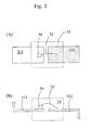
FIG. 1 is an LED cassette unit 200 which is disclosed in U.S. Pat. No. 7,445,355. The LED cassette unit 200 has a top metal electrode 21 and a bottom metal electrode 22. An insulation layer 25 is sandwiched in between the top metal electrode 21 and the bottom metal electrode 22. A center void is made in a center of the top metal electrode 21 and the insulation layer 25 to expose a center surface of the bottom metal electrode 22. An LED 20 is mounted on the bottom metal electrode 22 in the center void. A metal wire 24 electrically couples a top electrode of the LED 20 to the top metal electrode 21. A bottom electrode of the LED 20 electrically contacts the bottom metal electrode 22. Protection glue 23 encapsulates the metal wire 24 and the LED 20 for ensuring the quality and reliability of the LED package.
SUMMARY
This summary is provided to introduce a selection of concepts in a simplified form that are further described below in the Detailed Description. This summary is not intended to identify key features of the claimed subject matter, nor is it intended to be used as an aid in determining the scope of the claimed subject matter.
In accordance with aspects of the present disclosure, a manufacturing process is provided for making an LED package. The manufacturing process includes: mounting an LED on an inner end of a first metal, wherein the LED is electrically coupled to the first metal; electrically coupling the LED to an inner end of a second metal by a metal wire; bending an outer end of the first metal in a first direction to form a top electrode of the LED package; bending an outer end of the second metal in a second direction opposite of the first direction to form a bottom electrode of the LED package; and enclosing the LED and the metal wire in a protection molding.
In accordance with another aspect of the present disclosure, an LED package is provided. The LED package includes a first I metal having a beam, a pair of c-shaped metals, and a pair of inverse c-shaped metals. The LED package also includes a second metal having an inverse c shape with a top flat and a bottom flat, wherein the bottom flat of the second metal forms a bottom electrode of the LED package, an LED mounted on and electrically coupled to one of the beam of the first I metal or the top flat of the second metal, wherein the LED is electrically coupled by a metal wire to the other of the beam of the first I metal or the top flat of the second metal, and a protection molding enclosing the LED and the wire.
In some embodiments of the LED package, each of the c-shaped metals has a top flat and a bottom flat, wherein the bottom flats of the c-shaped metals extend from a first side of the beam and the top flats of the c-shaped metals form top electrodes of the LED package. In these embodiments and/or other embodiments of the LED package, each of the inverse c-shaped metals has a top flat and a bottom flat, wherein the bottom flats of the inverse c-shaped metals extend from a second side of the beam and the top flats of the inverse c-shaped metals forming top electrodes of the LED package.
In accordance with another aspect of the present disclosure, a manufacturing process is provided for making an LED package. The manufacturing process includes: mounting an LED on a beam of an I metal such that the LED is electrically coupled to the beam, wherein the I metal has a pair of c-shaped metals and a pair of inverse c-shaped metals; electrically coupling the LED to a second metal by a metal wire, wherein the second metal has an inverse c shape with a top flat and a bottom flat, and wherein the bottom flat of the second metal forms a bottom electrode of the LED package, and enclosing the LED and the metal wire in a protection molding.
In some embodiments of the manufacturing process, each of the c-shaped metals has a top flat and a bottom flat, wherein the top flats of the c-shaped metals form top electrodes of the LED package and the bottom flats of the c-shaped metals extend from a first side of the beam. In these and/or other embodiments of the manufacturing process, each of the inverse c-shaped metals has a top flat and a bottom flat, wherein the top flats of the inverse c-shaped metals form top electrodes of the LED package and the bottom flats of the inverse c-shaped metals extend from a second side of the beam.
In accordance with yet another aspect of the present disclosure, a manufacturing process is provided for making an LED package. The manufacturing process includes preparing a c-shaped metal by bending a first metal upwards twice 90 degrees, wherein the c-shaped metal has a top flat and a bottom flat, and wherein the top flat forms a top electrode of the LED package. The manufacturing process also includes preparing an inverse c-shaped metal by bending a second metal downwards twice 90 degrees, wherein the inverse c-shaped metal has a top flat and a bottom flat, and wherein the bottom flat forms a bottom electrode of the LED package. The manufacturing process further includes electrically coupling an LED to the bottom flat of the c-shaped metal and to the top flat of the inverse c-shaped metal, and enclosing the LED in a protection molding.
DESCRIPTION OF THE DRAWINGS
The foregoing aspects and many of the attendant advantages of this disclosure will become more readily appreciated as the same become better understood by reference to the following detailed description, when taken in conjunction with the accompanying drawings, wherein:
FIG. 1A shows a top view of a prior art LED cassette unit;
FIG. 1B shows a side view of the prior art LED cassette unit;
FIG. 2A shows a top view of a first embodiment of an LED package prior to bending in accordance with one or more embodiments of the present disclosure;
FIG. 2B shows a side view of the first embodiment of the LED package prior to bending in accordance with one or more embodiments of the present disclosure;
FIG. 3A shows a top view of the first embodiment of the LED package after bending in accordance with one or more embodiments of the present disclosure;
FIG. 3B shows a side view of the first embodiment of the LED package after bending in accordance with one or more embodiments of the present disclosure;
FIG. 4A shows a top view of a second embodiment of an LED package prior to bending in accordance with one or more embodiments of the present disclosure;
FIG. 4B shows a side view of the second embodiment of the LED package prior to bending in accordance with one or more embodiments of the present disclosure;
FIG. 5A shows a top view of the second embodiment of the LED package after bending in accordance with one or more embodiments of the present disclosure;
FIG. 5B shows a side view of the second embodiment of the LED package after bending in accordance with one or more embodiments of the present disclosure;
FIG. 6A shows a top view of the second embodiment of the LED package after bending in accordance with one or more embodiments of the present disclosure;
FIG. 6B shows a bottom view of the second embodiment of the LED package after bending in accordance with one or more embodiments of the present disclosure;
FIG. 6C shows a side view of the second embodiment of the LED package after bending in accordance with one or more embodiments of the present disclosure; and
FIG. 6D shows another side view of the second embodiment of the LED package after bending in accordance with one or more embodiments of the present disclosure.
DETAILED DESCRIPTION
An improved manufacturing process to manufacture an LED package with a top electrode and a bottom electrode is disclosed. The process includes preparing a piece of metal sheet, forming a pair of coplanar metals, namely, a first metal and a second metal, mounting an LED chip on an inner end of the first metal, wire-bonding a top electrode of the LED chip to an inner end of the second metal, molding to protect at least the LED chip and the bonding wire, bending an outer end of the first metal upward to form an extended flat top electrode, and bending an outer end of the second metal downward to form an extended bottom flat electrode.
FIGS. 2A, 2B, 3A, and 3B show different views of a first embodiment according to the present disclosure.
FIG. 2A shows a first embodiment before bending the metals according to the present disclosure. The process includes: (1) preparing a single piece of metal sheet (not shown), (2) forming a first metal 511 and a coplanar second metal 512 by, for example, punching the single piece of metal sheet, (3) mounting an LED 50 on an inner end of the first metal 511 and electrically coupling a bottom electrode of the LED 50 to the first metal 511, (4) electrically coupling a top electrode of the LED 50 to an inner end of the second metal 512 through wire-bonding with a metal wire 52, and (5) protection-molding with glue 53 for fixing and protecting at least the LED 50, the wire 52, and the inner ends of the two metals 511, 512.
FIG. 2B shows a side view of FIG. 2A. An outer end of the first metal 511 exposed outside of the glue 53 is going to be bent upward, and an outer end of the second metal 512 exposed outside of the glue 53 is going to be bent downward.
FIG. 3A shows a top view after bending of the metals 511, 512 according to the present disclosure. The outer end of the first metal 511 is bent upward twice 90 degrees to form a top flat 511T as a first extended electrode. The outer end of the second metal 512 is bent downward twice 90 degrees to form a bottom flat 512B as a second extended electrode.
FIG. 3B shows a side view of FIG. 3A. The outer end of the first metal 511 is bent to form a c-shaped top flat 511T as a top electrode of the package. The outer end of the second metal 512 is bent to form an inverse c-shaped bottom flat 512B as a bottom electrode of the package.
FIGS. 4A, 4B, 5A, 5B, and 6A-6D show different views of a second embodiment according to the present disclosure.
FIG. 4A shows a second embodiment before bending the metals according to the present disclosure. The process includes: (1) preparing a single metal sheet (not shown), (2) forming an I metal 611 (first metal) and a coplanar rectangular metal 612 (second metal); the I metal 611 has a vertical beam, a first pair of horizontal legs extended from a first side of the vertical beam, and a second pair of horizontal legs extended from a second side of the vertical beam; the rectangular metal 612 is located in between one of the two pairs of horizontal legs, (3) mounting an LED 60 on the vertical beam of the I metal 611, electrically coupling a bottom electrode of the LED 60 to the I metal 611 through direct contact, (4) electrically coupling a top electrode of the LED 60 to an inner end of the rectangular metal 612 through wire-bonding with a metal wire 62, and (5) protection-molding with glue 63 for fixing and protecting at least the LED 60, the metal wire 62, and the inner end of the rectangular metal 612.
FIG. 4B shows a side view of FIG. 4A. Outer ends of the four horizontal legs of the I metal 611 are exposed outside of the glue 63, with each of the four horizontal legs to be bent upward, and an outer end of the rectangular metal 612 exposed outside of the glue 63 to be bent downward.
FIG. 5A shows a top view after bending the horizontal legs of the I metal 611 and the rectangular metal 612 according to the present disclosure. Each of the outer ends of the four horizontal legs of the I metal 611 is bent upward twice 90 degrees to form four top flats 611T as extended top electrodes of the LED package. The outer end of the rectangular metal 612 is bent downward twice 90 degrees to form a bottom flat 612B as an extended bottom electrode of the LED package.
FIG. 5B shows a side view of FIG. 5A. The first pair of horizontal legs from the first side of the I metal 611 are bent to form a pair of c-shaped metals with two top flats 611T, a first top electrode and a second top electrode of the package. The second pair of horizontal legs from the second side of the I metal 611 are bent to form a pair of inverse c-shaped metals with two top flats 611T as a third top electrode and a fourth top electrode of the package. The rectangular metal 612 is bent to form an inverse c-shaped metal with the bottom flat 612B as a bottom electrode of the LED package.
FIG. 6A shows a top view of the LED package shown in FIGS. 5A and 5B. Four top flats 611T are shown which function as extended top electrodes of the LED package.
FIG. 6B shows a bottom view of the LED package shown in FIGS. 5A and 5B. The bottom flat 612B is shown which functions as a bottom electrode of the LED package.
FIG. 6C shows a first side view of the LED package shown in FIGS. 5A and 5B. The first pair of horizontal legs from the first side of the I metal 611 and the two top flats 611T are shown on the first side of the LED package.
FIG. 6D shows a second side view of the LED package shown in FIGS. 5A and 5B. The second pair of horizontal legs from the second side of the I metal 611, the two top flats 611T, and the rectangular metal 612 are shown on the second side of the LED package.
While several embodiments have been described by way of example, it will be apparent to those skilled in the art that various modifications may be made without departing from the spirit of the claimed subject matter. Such modifications are all within the scope of the present disclosure, as defined by the appended claims.

Claims (12)

The embodiments of the invention in which an exclusive property or privilege is claimed are defined as follows:
1. An LED package, comprising:
a first I metal having a beam, a pair of c-shaped metals, and a pair of inverse c-shaped metals, wherein:
each of the c-shaped metals has a top flat and a bottom flat, wherein the bottom flats of the c-shaped metals extend from a first side of the beam and the top flats of the c-shaped metals form top electrodes of the LED package; and
each of the inverse c-shaped metals has a top flat and a bottom flat, wherein the bottom flats of the inverse c-shaped metals extend from a second side of the beam and the top flats of the inverse c-shaped metals form top electrodes of the LED package;
a second metal having an inverse c shape with a top flat and a bottom flat, wherein the bottom flat of the second metal forms a bottom electrode of the LED package;
an LED mounted on and electrically coupled to one of the beam of the first I metal or the top flat of the second metal, wherein the LED is electrically coupled by a metal wire to the other of the beam of the first I metal or the top flat of the second metal; and
a protection molding enclosing the LED and the metal wire.
2. The LED package of claim 1, wherein a top surface of the top flats of the pair of c-shaped metals and a top surface of the top flats of the pair of inverse c-shaped metals extend outside the protection molding to form the top electrodes of the LED package.
3. The LED package of claim 1, wherein a bottom surface of the bottom flat of the second metal extends outside the protection molding to form the bottom electrode of the LED package.
4. The LED package of claim 1, wherein the protection molding further encloses the beam.
5. The LED package of claim 1, wherein the protection molding further encloses the bottom flats of the pair of c-shaped metals.
6. The LED package of claim 1, wherein the protection molding further encloses the top flat of the second metal.
7. The LED package of claim 1, wherein the protection molding further encloses the bottom flats of the inverse c-shaped metals.
8. The LED package of claim 1, wherein the bottom flats of the c-shaped metals, the bottom flats of the inverse c-shaped metals, and the top flat of the second metal are coplanar.
9. The LED package of claim 8, wherein the protection molding further encloses the bottom flats of the inverse c-shaped metals and the top flat of the second metal.
10. The LED package of claim 1, wherein a side surface of the top flats of the pair of c-shaped metals extends outside the protection molding.
11. The LED package of claim 1, wherein a side surface of the top flats of the pair of inverse c-shaped metals extends outside the protection molding.
12. The LED package of claim 1, wherein a side surface of the bottom flat of the second metal extends outside the protection molding to form the bottom electrode of the LED package.
US14/014,324 2009-07-16 2013-08-29 LED package with top and bottom electrodes Active US8710540B2 (en)

Priority Applications (2)

Application Number Priority Date Filing Date Title
US14/014,324 US8710540B2 (en) 2009-07-16 2013-08-29 LED package with top and bottom electrodes
US14/205,318 US8802503B2 (en) 2009-07-16 2014-03-11 Processes for manufacturing an LED package with top and bottom electrodes

Applications Claiming Priority (6)

Application Number Priority Date Filing Date Title
TW098124031 2009-07-16
TW098124031A TWI411139B (en) 2009-07-16 2009-07-16 Led package with top-bottom electrodes
TW98124031A 2009-07-16
US12/554,189 US8247835B2 (en) 2009-07-16 2009-09-04 LED package with top and bottom electrodes
US13/548,067 US8524541B2 (en) 2009-07-16 2012-07-12 Processes for manufacturing an LED package with top and bottom electrodes
US14/014,324 US8710540B2 (en) 2009-07-16 2013-08-29 LED package with top and bottom electrodes

Related Parent Applications (1)

Application Number Title Priority Date Filing Date
US13/548,067 Division US8524541B2 (en) 2009-07-16 2012-07-12 Processes for manufacturing an LED package with top and bottom electrodes

Related Child Applications (1)

Application Number Title Priority Date Filing Date
US14/205,318 Division US8802503B2 (en) 2009-07-16 2014-03-11 Processes for manufacturing an LED package with top and bottom electrodes

Publications (2)

Publication Number Publication Date
US20140042483A1 US20140042483A1 (en) 2014-02-13
US8710540B2 true US8710540B2 (en) 2014-04-29

Family

ID=43464665

Family Applications (4)

Application Number Title Priority Date Filing Date
US12/554,189 Active 2030-11-19 US8247835B2 (en) 2009-07-16 2009-09-04 LED package with top and bottom electrodes
US13/548,067 Active US8524541B2 (en) 2009-07-16 2012-07-12 Processes for manufacturing an LED package with top and bottom electrodes
US14/014,324 Active US8710540B2 (en) 2009-07-16 2013-08-29 LED package with top and bottom electrodes
US14/205,318 Active US8802503B2 (en) 2009-07-16 2014-03-11 Processes for manufacturing an LED package with top and bottom electrodes

Family Applications Before (2)

Application Number Title Priority Date Filing Date
US12/554,189 Active 2030-11-19 US8247835B2 (en) 2009-07-16 2009-09-04 LED package with top and bottom electrodes
US13/548,067 Active US8524541B2 (en) 2009-07-16 2012-07-12 Processes for manufacturing an LED package with top and bottom electrodes

Family Applications After (1)

Application Number Title Priority Date Filing Date
US14/205,318 Active US8802503B2 (en) 2009-07-16 2014-03-11 Processes for manufacturing an LED package with top and bottom electrodes

Country Status (2)

Country Link
US (4) US8247835B2 (en)
TW (1) TWI411139B (en)

Families Citing this family (1)

* Cited by examiner, † Cited by third party
Publication number Priority date Publication date Assignee Title
CN111081162B (en) * 2020-01-07 2022-01-25 深圳市丽晶光电科技股份有限公司 Process for solving flatness of display screen module

Citations (6)

* Cited by examiner, † Cited by third party
Publication number Priority date Publication date Assignee Title
US6433418B1 (en) 1998-07-24 2002-08-13 Fujitsu Limited Apparatus for a vertically accumulable semiconductor device with external leads secured by a positioning mechanism
US20020140079A1 (en) 2001-03-23 2002-10-03 Yoshifumi Takeyama Mounting structure and mounting method of a photovoltaic element, mounting substrate for mounting a semiconductor element and method for mounting said semiconductor element on said mounting substrate
US20050280158A1 (en) 1994-03-11 2005-12-22 Silicon Bandwidth, Inc. Prefabricated semiconductor chip carrier
US20080073762A1 (en) 2006-09-21 2008-03-27 Samsung Electronics Co. Ltd. Semiconductor device package
US7445355B2 (en) 2006-02-17 2008-11-04 Jiahn-Chang Wu Matrix display using cassette light units
TWM350827U (en) 2008-09-09 2009-02-11 I Chiun Precision Ind Co Ltd Improved supporting stand for SMD type of light emitting diode

Family Cites Families (1)

* Cited by examiner, † Cited by third party
Publication number Priority date Publication date Assignee Title
US5969427A (en) 1998-02-05 1999-10-19 Micron Technology, Inc. Use of an oxide surface to facilitate gate break on a carrier substrate for a semiconductor device

Patent Citations (6)

* Cited by examiner, † Cited by third party
Publication number Priority date Publication date Assignee Title
US20050280158A1 (en) 1994-03-11 2005-12-22 Silicon Bandwidth, Inc. Prefabricated semiconductor chip carrier
US6433418B1 (en) 1998-07-24 2002-08-13 Fujitsu Limited Apparatus for a vertically accumulable semiconductor device with external leads secured by a positioning mechanism
US20020140079A1 (en) 2001-03-23 2002-10-03 Yoshifumi Takeyama Mounting structure and mounting method of a photovoltaic element, mounting substrate for mounting a semiconductor element and method for mounting said semiconductor element on said mounting substrate
US7445355B2 (en) 2006-02-17 2008-11-04 Jiahn-Chang Wu Matrix display using cassette light units
US20080073762A1 (en) 2006-09-21 2008-03-27 Samsung Electronics Co. Ltd. Semiconductor device package
TWM350827U (en) 2008-09-09 2009-02-11 I Chiun Precision Ind Co Ltd Improved supporting stand for SMD type of light emitting diode

Also Published As

Publication number Publication date
TWI411139B (en) 2013-10-01
US20110012162A1 (en) 2011-01-20
US8802503B2 (en) 2014-08-12
US20120273835A1 (en) 2012-11-01
US8524541B2 (en) 2013-09-03
US8247835B2 (en) 2012-08-21
US20140042483A1 (en) 2014-02-13
TW201104924A (en) 2011-02-01
US20140193930A1 (en) 2014-07-10

Similar Documents

Publication Publication Date Title
US8184453B1 (en) Increased capacity semiconductor package
US6700189B2 (en) Resin sealed semiconductor device
JP6370071B2 (en) Semiconductor device and manufacturing method thereof
JP4698234B2 (en) Surface mount semiconductor device
US9013030B2 (en) Leadframe, semiconductor package including a leadframe and method for producing a leadframe
JP2009500841A (en) Semiconductor device
KR20080022452A (en) Pop package and method of producing the same
TWI634634B (en) Semiconductor device and method of manufacturing the same
US9029993B2 (en) Semiconductor device including semiconductor chip mounted on lead frame
JP4530863B2 (en) Resin-sealed semiconductor device
JP2009064854A (en) Lead frame, semiconductor device, and manufacturing method of semiconductor device
US20110049686A1 (en) Semiconductor package and method of manufacturing the same
US8609527B2 (en) Method of manufacturing semiconductor device
US8710540B2 (en) LED package with top and bottom electrodes
US20140217602A1 (en) Semiconductor device
CN110892526B (en) Method for manufacturing semiconductor device
JP6909630B2 (en) Semiconductor device
US9299645B2 (en) Semiconductor device having lead frame with notched inner leads
US8581384B2 (en) Semiconductor package structure
JP2009182230A (en) Resin sealing type semiconductor device, and method of manufacturing the same
JP4514497B2 (en) Manufacturing method of semiconductor device
JP6909629B2 (en) Semiconductor device
JPH02278857A (en) Resin-sealed type semiconductor device
US20090079045A1 (en) Package structure and manufacturing method thereof
KR20020024654A (en) Stacking -type semiconductor package unit and stacking-type semiconductor package

Legal Events

Date Code Title Description
AS Assignment

Owner name: CHENG KUNG CAPITAL, LLC, DELAWARE

Free format text: ASSIGNMENT OF ASSIGNORS INTEREST;ASSIGNOR:WU, JIAHN-CHANG;REEL/FRAME:031117/0709

Effective date: 20110805

STCF Information on status: patent grant

Free format text: PATENTED CASE

MAFP Maintenance fee payment

Free format text: PAYMENT OF MAINTENANCE FEE, 4TH YEAR, LARGE ENTITY (ORIGINAL EVENT CODE: M1551)

Year of fee payment: 4

MAFP Maintenance fee payment

Free format text: PAYMENT OF MAINTENANCE FEE, 8TH YEAR, LARGE ENTITY (ORIGINAL EVENT CODE: M1552); ENTITY STATUS OF PATENT OWNER: LARGE ENTITY

Year of fee payment: 8