US8664596B2 - Method for characterizing identified defects during charged particle beam inspection and application thereof - Google Patents
Method for characterizing identified defects during charged particle beam inspection and application thereof Download PDFInfo
- Publication number
- US8664596B2 US8664596B2 US12/489,804 US48980409A US8664596B2 US 8664596 B2 US8664596 B2 US 8664596B2 US 48980409 A US48980409 A US 48980409A US 8664596 B2 US8664596 B2 US 8664596B2
- Authority
- US
- United States
- Prior art keywords
- temperature
- defects
- sample
- defect
- distribution map
- Prior art date
- Legal status (The legal status is an assumption and is not a legal conclusion. Google has not performed a legal analysis and makes no representation as to the accuracy of the status listed.)
- Expired - Fee Related, expires
Links
- 230000007547 defect Effects 0.000 title claims abstract description 296
- 239000002245 particle Substances 0.000 title claims abstract description 60
- 238000007689 inspection Methods 0.000 title claims abstract description 53
- 238000000034 method Methods 0.000 title claims abstract description 25
- 238000003384 imaging method Methods 0.000 claims abstract description 52
- 238000012360 testing method Methods 0.000 claims description 32
- 239000000523 sample Substances 0.000 description 107
- 238000010586 diagram Methods 0.000 description 11
- 238000001816 cooling Methods 0.000 description 9
- 238000010438 heat treatment Methods 0.000 description 9
- 230000002950 deficient Effects 0.000 description 8
- 239000004065 semiconductor Substances 0.000 description 8
- 238000010191 image analysis Methods 0.000 description 6
- 230000002159 abnormal effect Effects 0.000 description 4
- 230000001419 dependent effect Effects 0.000 description 4
- 238000013459 approach Methods 0.000 description 3
- 230000007423 decrease Effects 0.000 description 3
- 238000001514 detection method Methods 0.000 description 3
- 238000009792 diffusion process Methods 0.000 description 3
- 235000012489 doughnuts Nutrition 0.000 description 3
- 230000007246 mechanism Effects 0.000 description 3
- 230000008859 change Effects 0.000 description 2
- 238000012512 characterization method Methods 0.000 description 2
- 238000004886 process control Methods 0.000 description 2
- 230000009471 action Effects 0.000 description 1
- 238000004458 analytical method Methods 0.000 description 1
- 239000002800 charge carrier Substances 0.000 description 1
- 230000003247 decreasing effect Effects 0.000 description 1
- 238000013461 design Methods 0.000 description 1
- 230000005684 electric field Effects 0.000 description 1
- 230000002708 enhancing effect Effects 0.000 description 1
- 230000007613 environmental effect Effects 0.000 description 1
- 238000004519 manufacturing process Methods 0.000 description 1
- 239000000463 material Substances 0.000 description 1
- 238000012986 modification Methods 0.000 description 1
- 230000004048 modification Effects 0.000 description 1
- 230000002085 persistent effect Effects 0.000 description 1
- 238000004451 qualitative analysis Methods 0.000 description 1
- 230000009467 reduction Effects 0.000 description 1
- 230000035945 sensitivity Effects 0.000 description 1
- 230000003068 static effect Effects 0.000 description 1
- 230000005641 tunneling Effects 0.000 description 1
Images


Classifications
-
- G—PHYSICS
- G01—MEASURING; TESTING
- G01N—INVESTIGATING OR ANALYSING MATERIALS BY DETERMINING THEIR CHEMICAL OR PHYSICAL PROPERTIES
- G01N23/00—Investigating or analysing materials by the use of wave or particle radiation, e.g. X-rays or neutrons, not covered by groups G01N3/00 – G01N17/00, G01N21/00 or G01N22/00
- G01N23/22—Investigating or analysing materials by the use of wave or particle radiation, e.g. X-rays or neutrons, not covered by groups G01N3/00 – G01N17/00, G01N21/00 or G01N22/00 by measuring secondary emission from the material
- G01N23/225—Investigating or analysing materials by the use of wave or particle radiation, e.g. X-rays or neutrons, not covered by groups G01N3/00 – G01N17/00, G01N21/00 or G01N22/00 by measuring secondary emission from the material using electron or ion
-
- H—ELECTRICITY
- H01—ELECTRIC ELEMENTS
- H01J—ELECTRIC DISCHARGE TUBES OR DISCHARGE LAMPS
- H01J37/00—Discharge tubes with provision for introducing objects or material to be exposed to the discharge, e.g. for the purpose of examination or processing thereof
- H01J37/26—Electron or ion microscopes; Electron or ion diffraction tubes
- H01J37/28—Electron or ion microscopes; Electron or ion diffraction tubes with scanning beams
-
- G—PHYSICS
- G01—MEASURING; TESTING
- G01N—INVESTIGATING OR ANALYSING MATERIALS BY DETERMINING THEIR CHEMICAL OR PHYSICAL PROPERTIES
- G01N2223/00—Investigating materials by wave or particle radiation
- G01N2223/60—Specific applications or type of materials
- G01N2223/611—Specific applications or type of materials patterned objects; electronic devices
- G01N2223/6116—Specific applications or type of materials patterned objects; electronic devices semiconductor wafer
-
- H—ELECTRICITY
- H01—ELECTRIC ELEMENTS
- H01J—ELECTRIC DISCHARGE TUBES OR DISCHARGE LAMPS
- H01J2237/00—Discharge tubes exposing object to beam, e.g. for analysis treatment, etching, imaging
- H01J2237/20—Positioning, supporting, modifying or maintaining the physical state of objects being observed or treated
- H01J2237/206—Modifying objects while observing
- H01J2237/2065—Temperature variations
-
- H—ELECTRICITY
- H01—ELECTRIC ELEMENTS
- H01J—ELECTRIC DISCHARGE TUBES OR DISCHARGE LAMPS
- H01J2237/00—Discharge tubes exposing object to beam, e.g. for analysis treatment, etching, imaging
- H01J2237/245—Detection characterised by the variable being measured
- H01J2237/24564—Measurements of electric or magnetic variables, e.g. voltage, current, frequency
-
- H—ELECTRICITY
- H01—ELECTRIC ELEMENTS
- H01J—ELECTRIC DISCHARGE TUBES OR DISCHARGE LAMPS
- H01J2237/00—Discharge tubes exposing object to beam, e.g. for analysis treatment, etching, imaging
- H01J2237/26—Electron or ion microscopes
- H01J2237/28—Scanning microscopes
- H01J2237/2803—Scanning microscopes characterised by the imaging method
Definitions
- the present invention relates to a method for imaging and characterizing defects on a semiconductor device which is sensitive to temperature with charged particle beam apparatus, and more particularly, to a method and apparatus for charged particle beam inspection of a semiconductor device with temperature control, and application thereof for characterizing the identified defects by separating, suppressing and/or enhancing specific defect types which are sensitive to temperature in electrical properties.
- Charged particle beam inspection tools are widely used in the semiconductor industry to examine physical and electrical defects in fabricated devices by observing the difference of grey level profile from the normal devices as a result of charging voltages difference induced by charged particle beam imaging.
- the image is also known as a voltage contrast (VC) image.
- VC voltage contrast
- a normal feature is expected to be well grounded while an open circuit defect may appear relatively dark in a VC image due to excessive positive charge accumulated (positive charging is induced by scanning the interested device with charged particle beam); this is generally referred to as a dark voltage contrast (DVC) defect.
- DVC dark voltage contrast
- BVC bright voltage contrast
- the short circuit defect and the sub-threshold leakage defect may both display as a BVC defect, but the meaning to process control and yield enhancement is totally different.
- a short circuit defect is a kind of electrical defect, which is resulted from, for example, a deformed plug contacting its neighboring plug. Also, voids or keyholes formed between contact plugs/vias may lead to a shorted device. This is generally referred to as “piping”.
- a short defect is fatal to a semiconductor device as it could cause the device inoperable.
- Leakage is another type of defect with strong dependency on threshold voltage (Vth) of the MOSFET devices. Intrinsic Vth varies with doping density, device dimension, thickness of gate oxide, and environmental factors such as applied voltage and temperature. Whether a leakage defect is fatal to a semiconductor device or not depends on the categories and applications of the devices.
- the leakage current For example, power consumption and performance of ICs are directly related to the leakage current.
- the leakage of individual devices which are not actively changing states is often referred to as the static power consumption and is generally negligible to devices when operating.
- the leakage defects may be treated as nuisance defects and need to be filtered out of the short-circuit defects and other killer defects.
- Vdd supply voltage
- Vth threshold voltage
- Charged particle beam inspection tool can be used to detect the short/leakage defects as abnormal VCs, but it is often difficult to distinguish between them due to their similar VC images. Also, as mentioned earlier, there are more requirements for inspecting the leakage defect more than just determining its presence, but also for pinpointing the level of leakage.
- a method for characterizing identified defects during charged particle beam inspection of a sample comprises obtaining a voltage contrast image of the sample by using a charged particle beam imaging apparatus at an inspection temperature; identifying, from the voltage contrast image, presence of at least one defect on the sample; providing reference data of the sample, wherein the reference data represents at least one reference defect on the sample; comparing the location or geographical distribution of the identified defects and the reference defects on the sample to correlate the identified defects with the inspection temperature thereby characterizing the identified defects.
- a charged particle beam inspection system comprises a charged particle beam imaging apparatus, a heating/cooling apparatus, and a defect determination apparatus.
- the charged particle beam imaging apparatus is for forming a voltage contrast image of a sample.
- the heating/cooling apparatus is for changing the temperature of the sample.
- the defect determination apparatus comprises a control module and an image analysis module.
- the control module is coupled to the charged particle beam imaging apparatus and the heating/cooling apparatus for coordinating these elements to control the temperature (the imaging temperature) of the sample when being imaged.
- the image analysis module is coupled with the charged particle beam imaging apparatus and the control module for receiving the voltage contrast image from the charged particle beam imaging apparatus and corresponding temperature information when imaging from the control module, so as to correlate defects of the sample identified from the voltage contrast image with the imaging temperatures, thereby characterizing the identified defects.
- FIG. 1 is a diagram illustrating the temperature dependency of the leakage components of a typical IC device
- FIGS. 2 a to 2 d are schematic diagrams illustrating occurrence of temperature-dependent defect
- FIG. 3 is a flow chart illustrating a method for characterizing identified defects during charged particle beam inspection of a sample in accordance with an embodiment of the present invention
- FIG. 4 a to FIG. 4 c are schematic diagrams illustrating execution of an inspection method by means of charged particle beam in accordance with an embodiment of the present invention
- FIG. 5 a to FIG. 5 c are diagrams respectively illustrating a defect distribution map produced from charged particle beam inspection of a sample performed at various temperatures;
- FIG. 6 is a schematic diagram illustrating of an electrical failure test result of the sample in FIG. 5 a ;
- FIG. 7 is a schematic diagram of a charged particle beam inspection according to an embodiment of the present invention.
- FIG. 1 is a diagram illustrating the temperature dependency of the leakage components of a typical IC device. As indicated, there are different mechanisms contributing to the overall leakage.
- the major leakage mechanism includes (1) Sub-threshold leakage, (2) gate leakage, and (3) reverse biased junction leakage. Each of these leakage components has different dependency on transistor geometry, material properties and supply voltage, and temperature.
- the sub-threshold leakage is a diffusion current of carrier flowing between source and drain.
- the sub-threshold leakage is a strong function of temperature at “off” state, that is to say, the state that supplied gate voltage is smaller than the device threshold voltage (Vgs ⁇ Vth).
- junction leakage results from the small minority carrier diffusion/drift current across the reverse biased junction.
- the junction leakage is also a function of temperature. Gate leakage is mainly because electrons tunneling across the oxide as a result of the high electrical field across the thin oxide layer, so it is relatively insensitive to temperature. Illustrated in FIG. 1 is also a short-circuit type defect which serves as another example of temperature-insensitive defect.
- the present invention makes use of the temperature-dependency property of a semiconductor device to separate the identified temperature-sensitive defects (for example, sub-threshold leakage and junction leakage) from temperature-insensitive defects (for example, electrically short-circuit defects, and gate leakage defects) and characterize the temperature-sensitive leakage defects by grey level from voltage contrast images.
- a short-circuit defect is an electrical defect due to physical contact, hence its grey level generally does not vary with temperature, as illustrated in FIG. 1 .
- a short defect can be distinguished from the temperature-dependent sub-threshold or junction leakage defect by lowering the temperature of the detected defects and observing whether their grey level changes.
- a gate leakage defect is temperature-insensitive, thus will behave similarly to a short-circuit defect (If necessary, It can be further differentiated from the short-circuit defect by varying the external field strength applied on the gate).
- the same principal applies that is, a defective leakage current flowing across the device will exist regardless of the temperature of the device, while a non-defective leakage current is less likely to be shown on a device at a low enough temperature.
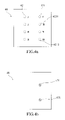
- FIGS. 2 a to 2 d are schematic diagrams illustrating occurrence of temperature-dependent defect.
- FIG. 2 a illustrates defects on a sample 200 detected by charged particle beam inspection performed at T 1 .
- Sample 200 may be a wafer.
- FIG. 2 b illustrates defects detected at T 2
- FIG. 2 c illustrates defects detected at T 3
- FIG. 2 d illustrates defects detected at T 4 .
- Temperature T 1 is higher than T 2
- T 2 is higher than T 3
- T 3 is higher than T 4 (T 1 >T 2 >T 3 >T 4 ).
- T 1 five defects 201 are detected.
- T 2 is higher than T 3
- T 3 is higher than T 4 (T 1 >T 2 >T 3 >T 4 ).
- T 1 five defects 201 are detected.
- T 2 is higher than T 3
- T 3 is higher than T 4 (T 1 >T 2 >T 3 >T 4 ).
- T 1 five defects 201 are detected.
- T 2 is higher than T
- This temperature-induced variation in the number of detected defects could cause inaccuracy to the inspection result, because in most cases the inspection is performed at arbitrary temperature, for example the room temperature for convenience, and thus the defects detected at the inspection temperature may not reflect the “real” defects on the sample that may affect the manufacture yield.
- a method for characterizing identified defects during charged particle beam inspection of a sample is disclosed.
- the sample can be a wafer.
- the sample is imaged using a charged particle beam imaging apparatus at a higher temperature and a lower temperature, respectively, and VC images of the sample at respective temperatures are obtained.
- Defects on the sample are identified from respective images, and the locations of these identified defects on the sample are recorded.
- this location information is used to produce a defect distribution map.
- a defect distribution map represents the identified defects, and their location or known as geographical distribution on the sample.
- the found higher and lower temperature defects could be of the same defect type with different sensitivities to temperature, or they could be different defect types or generated from different root causes, but result in substantially the same or at least similar abnormal electrical properties of the sample.
- all short defects, junction leakage defects and sub-threshold leakage defects lead to undesired electrical connection within a device.
- the higher and lower temperature defects should display the same or similar grey level in the obtained grey level image, such as a bright voltage contrast (BVC).
- BVC bright voltage contrast
- the location of the higher temperature defects on the sample is compared with the location of the lower temperature defects on the sample. If a higher temperature defect is found at the same position corresponding to lower temperature, such higher temperature defect is said to be a “common defect”. In other words, the common defect is a defect which is observed at a higher temperature, and remains as an observable defect when the temperature is lowered. Higher temperature defects that do not have corresponding lower temperature defects located at the same position on the sample will be referred to as “non-common” defects hereinafter.
- the lower temperature image is used as a reference for finding the above defined common defects.
- the common defect is considered to be more serious than the non-common defect, as it is more persistent by showing up even at the lower temperature.
- the found defects are leakage defects
- the common leakage defects should be of a higher level of leakage than the non-common ones.
- the non-common defects on the contrary, as they have a sensitive temperature-dependent behavior over the given temperature range, are less likely to be an issue toward operation of the interested device they are located on.
- the purpose of finding the common defects is to correlate the higher temperature defects with the higher temperature so that temperature can become an index for characterizing the found defects.
- a wafer may first be inspected at a very high and a very low temperature regime.
- a large quantity of defects (leakage defects plus short defects) tends to be detected.
- a threshold for an intolerable number of total defects can be predefined, thus at a high enough temperature the number of detected defects will reach this threshold.
- the low temperature regime on the other hand, a smaller quantity of defects tends to be detected. If the imaging temperature is low enough, only temperature-insensitive defects (e.g. short defects) will show, for example, showing in the defect distribution map. The defect distribution map at such temperature can thus serve as a reference of inspection for the interested sample.
- the detected temperature-insensitive defects (for example short defects) on the sample are the common defects, and the detected temperature-sensitive leakage defects (e.g. sub-threshold leakage) are the non-common defects. Therefore, the temperature-sensitive leakage defects can be filtered out when the higher temperature inspection result is interpreted with reference to the lower temperature defect distribution map.
- the lower imaging temperature can be selected so that both the temperature insensitive defects (e.g. short defects) and serious temperature-sensitive leakage defects (e.g. sub-threshold leakage) are represented in the lower temperature defect distribution map. Therefore, nuisance leakage defects can be filtered out when the higher temperature inspection result is interpreted with reference to the lower temperature defect distribution map.
- the temperature insensitive defects e.g. short defects
- serious temperature-sensitive leakage defects e.g. sub-threshold leakage
- the VC behavior of the interested sample in individual obtained grey level images reveals the abnormal electrical properties of the interested sample at corresponding imaging temperature when a lower temperature inspection result is available as a reference.
- the number of the temperature-insensitive defects (short defects and/or gate leakage defects) as well as the temperature-sensitive defects (sub-threshold and/or junction leakage defects) on the sample can be estimated.
- the two numbers combined may make the sample to be considered defective. If the number of the temperature-insensitive defects itself exceeds a tolerable threshold, the sample is considered defective.
- the total number of detected defects can be compared with a tolerable threshold value to determine if the inspected device is acceptable, or further analysis such as more temperature-based inspections may be performed to exclude the nuisance temperature-sensitive leakage defects.
- an electrical failure test result of the interested devices on the sample is used as the reference.
- the electrical failure test is a test that can identify the defective devices on the sample based on electrical failures.
- the test parameters can be selected to carry out the detection of leakage defects on the sample.
- the electrical failure test is typically performed at the operating temperature of the interested devices on the sample.
- the defects indicated by the electrical failure test are the ones that will fail at the desired operational condition. In other words, they are the “real” defects. It is noted that the temperature of the electrical failure test could be higher, equal to or lower that the higher temperature at which the charged particle beam inspection is performed.
- the location of the higher temperature defects are compared with the location of the electrical failure defects identified from the electrical failure test result.
- the geographical distribution of the higher temperature defects on the sample e.g. a wafer
- the geographical distribution of electrical failure defects on the sample is compared with the geographical distribution of electrical failure defects on the sample.
- Such comparison can be a qualitative analysis, for instance, considering the shape of defect distribution over the sample.
- the electrical failure test is set to detect sub-threshold leakage defects on a sample, and the detected defects are distributed over the sample in a certain shape.
- the shape of distribution of the higher temperature defects over the sample is similar to that of the detected electrical failure defects, it is determined that the inspection performed at the higher temperature substantially catches the presence of the interested defects, the sub-threshold leakage defects.
- the “shape” of defect distribution can be, for example, a donut shape on the outer rim portion of the wafer, or randomly distributed on the center portion of the wafer etc.
- similarity degree of the defect distribution shapes is determined arbitrarily.
- a series of images, each formed at a corresponding imaging temperature are compared with the electrical failure test result performed at a designated temperature.
- This designated temperature may be selected to be the operating temperature of the interested devices on the sample, for example, the room temperature.
- Defects on the sample are identified from respective images, and the locations of these identified defects on the sample are recorded, so that for each imaging temperature, a shape in which the identified defects are distributed over the sample is recognized. Then, these defect distribution shapes at different imaging temperatures are compared with the defect distribution shapes observed from the electrical failure test result. A most matched distribution shape of the higher temperature defects to the electrical failure defects is determined, and the corresponding imaging temperature is considered to be suitable for inspection of the interested sample.
- FIG. 3 is a flow chart illustrating a method for characterizing identified defects during charged particle beam inspection of a sample in accordance with an embodiment of the present invention.
- the method comprises the following steps.
- a first voltage contrast image of the sample is obtained at a first imaging temperature by using a charged particle beam imaging apparatus.
- the first imaging temperature may be selected to be within a range of ⁇ 50° C. to 350° C. In one embodiment, the first imaging temperature is selected to be room temperature.
- step 12 the presence of at least one first temperature defect on the sample is identified, for example, by observing a grey level profile of the sample displayed in the first voltage contrast image. It is noted that the purpose of step 12 is to identify detects from the first voltage contrast image; several well known approaches of image inspection can be used to carry out step 12 , and the details of these approaches will not be described here to avoid unnecessary limitations on the present invention. Examples of well known image inspection approaches include die-to-die mode inspection, array mode inspection, die-to-database mode inspection, etc.
- FIG. 4 a illustrates the above first voltage contrast image obtained from step 10 .
- a voltage contrast image 40 comprises a grey level profile 42 displayed therewithin.
- the grey level profile 42 includes an array of spots 421 which displays various grey levels.
- Spots 421 may represent, for example, conductive plugs within a semiconductor device such as contact plugs within a MOSFET device.
- grey level of individual spots 421 are represented in numbers, as illustrated in FIG. 4 a . The higher the grey level is, the brighter the spot 421 is.
- spot 4211 and 4212 are identified as a BVC defect from image 40 , which is the first temperature defect described earlier in step 12 . It is noted that it is not a necessary condition that spot 4211 and 4212 have the same grey level ( 150 ) in FIG. 4 a ; the grey level of spot 4211 and 4212 can be different.
- step 14 the location of the identified first temperature defects is recorded and used to produce a first defect distribution map accordingly, wherein the first defect distribution map represents the identified first temperature defects and their location on the sample.
- the first defect distribution map represents the geographical distribution of the first temperature defects on the sample.
- the first defect distribution map may be generated through implementation of software.
- FIG. 4 b illustrates a first defect distribution map 46 , which is formed from voltage contrast image 40 . As illustrated in FIG. 4 b , in first defect distribution map 46 , two identified first temperature defects 471 and 472 from image 40 are shown.
- a reference defect distribution map is provided, wherein the reference defect distribution map represents at least one reference defect and location thereof on the sample.
- the reference defect distribution map represents the geographical distribution of the reference defects on the sample.
- the reference defect distribution map is a second defect distribution map produced from a second voltage contrast image of the sample obtained from inspection performed at a second imaging temperature, wherein the second defect distribution map represents at least one second temperature defect and location (geographical distribution) thereof on the sample.
- the second imaging temperature may be selected to be within a range of ⁇ 50° C. to 350° C. It is noted that to be the reference, the second imaging temperature is preferably selected to be lower than the first imaging temperature.
- FIG. 4 c illustrates a second defect distribution map 48 . As illustrated in FIG. 4 c , in second defect distribution map 48 , one identified second temperature defect 49 is shown.
- the first defect distribution map and the reference defect distribution map are compared for characterization of the first temperature defects.
- the comparison is to determine the presence of at least one of the first temperature defects which has a locationally corresponding reference defect on the sample. If such reference defect exists, the considered first temperature defect is categorized as a common defect.
- the rest first temperature defects on the other hand, are categorized as non-common defects.
- First temperature defect 471 in first defect distribution map 46 has a locationally corresponding second temperature defect 49 in second defect distribution map 48 , while the other first temperature defect 472 does not. Therefore, in this embodiment, first temperature defect 471 will be categorized as a common defect and first temperature defect 472 will be categorized as a non-common defect.
- the reference defect distribution map is selected to be an electrical failure test result of the sample, and the reference defects are those determined by the electrical failure test performed.
- the produced first defect distribution map is compared with the reference defect distribution map to see how well the shape of distribution of the first temperature defects matches the shape of distribution of the reference defects on the sample. The result is then used to help select a suitable temperature for inspection of the interested sample.
- FIG. 5 a to FIG. 5 c are three diagrams respectively illustrating a defect distribution map 510 which is produced from charged particle beam inspection of a sample 500 performed at an imaging temperature T 510 , a defect distribution map 520 for an imaging temperature T 520 , and a defect distribution map 530 for an imaging temperature T 530 in accordance with an embodiment of the present invention.
- Temperature T 510 is higher than temperature T 520
- temperature T 520 is higher than temperature T 530 (T 510 >T 520 >T 530 ).
- sample 500 is a wafer which includes a plurality of dies formed thereon.
- the dies are represented in small squares, as shown in FIGS. 5 a to 5 c .
- the detected defects are represented in the form of bad dies on sample 500 , wherein a bad die is defined to have a quantity of defects thereon which exceeds a pre-selected threshold.
- the bad dies are represented in the maps as dark squares. Grey squares indicate dies having relatively fewer defects and are less defective as compared to the dark black squares.
- map 510 it can be seen from map 510 to map 530 that the number of detected defects decreases with temperature, but the fundamental shape of distribution of the defects, which is a donut shape, retains in all maps.
- map 510 and 520 there are a group of bad dies located on the lower portion of sample 500 .
- the number of these bad dies decreases from map 510 (obtained at T 510 ) to map 520 (obtained at T 520 which is lower than T 510 ).
- map 530 substantially all these bad dies disappear.
- bad dies distributed on the outer rim portion of sample 500 are present in all maps. Therefore, in this case it may be inferred that the defects distributed on the outer rim portion of sample 500 are more likely to be temperature-insensitive (e.g. short or gate leakage) defects or serious temperature-sensitive (e.g. severe sub-threshold or junction leakage) defects, while the defects distributed on the lower portion of sample 500 are more likely to be less temperature-sensitive leakage defects. For example, they could be nuisance leakage defects.
- FIG. 6 is a schematic diagram illustrating an electrical failure test result 60 of sample 500 in FIG. 5 a .
- the electrical failure test is performed on the same sample 500 and may be selected to be performed at a predefined test temperature, for example at the room temperature or the desired operating temperature of the interested devices on sample 500 .
- the target defect to be tested should be of the same type as that which was detected by charged particle beam inspection in the embodiment of FIG. 5 .
- the interested defect type(s) of both the test and the inspection should at least cause substantially the same abnormal electrical property to sample 500 .
- both the inspection and the test are to detect short or leakage defects that lead to undesired electrical connection within sample 500 .
- the identified defects again represented as bad dies, are distributed mostly on the outer rim region of sample 500 and form a donut shape.
- defect distribution maps 510 , 520 and 530 are then compared with electrical failure test result 60 . It can be seen from FIG. 5 and FIG. 6 that defect distribution map 530 best matches electrical failure test result 60 in terms of the shape of distribution of the identified defects and reference defects. Therefore, in this embodiment, T 530 will be selected to be the most suitable temperature, of the three temperatures T 510 , T 520 and T 530 , for inspection of sample 500 .
- the defect distribution map not only the number of the identified defects can be estimated, but also the geographical distribution of the defects on the sample can be analyzed. This can be useful in certain inspection job scenarios. For example, some areas on the sample may comprise particular type(s) of devices which is sensitive to sub-threshold leakage defects. Therefore, a proper threshold, for example the number of sub-threshold leakage defects, may be applied for determining the yield of these areas. Other determination may involve power consumption or performance requirements of the interested devices. For example, the power consumption performance of the device may be defined, whereby the limitation on the leakage current flowing across the device may be estimated.
- the present invention can be used to suppress or enhance particular defects sensitive to the temperature.
- the sample may be heated during or prior to the inspection to stimulate sub-threshold and/or junction leakage, so that these temperature-sensitive leakage defects can be detected.
- the sample may be cooled during or prior to the inspection to suppress the sub-threshold and/or junction leakage, so that the temperature-insensitive defects (such as the short defect and/or the gate leakage defect) can be distinguished from the temperature-sensitive leakage defects.
- a charged particle beam inspection system is disclosed.
- FIG. 7 is a schematic diagram of a charged particle beam inspection system according to an embodiment of the present invention.
- a charged particle beam inspection system 700 comprises a charged particle beam imaging apparatus 710 , a heating/cooling apparatus 720 , and a defect determination apparatus 730 .
- Charged particle beam imaging apparatus 710 is for forming a voltage contrast image of an interested sample.
- Heating/cooling apparatus 720 is for causing temperature change to the interested sample.
- Defect determination apparatus 730 comprises a control module 731 and an image analysis module 732 .
- Control module 731 is coupled to charged particle beam imaging apparatus 710 and heating/cooling apparatus 720 for coordinating these elements such that when the interested sample is being imaged, its temperature, which will be referred to as the imaging temperature hereinafter, is properly controlled for the purpose of characterizing the identified defects.
- control module 731 also collects temperature information of the interested sample from heating/cooling apparatus 720 .
- Image analysis module 732 is coupled with charged particle beam imaging apparatus 710 and control module 731 for receiving the voltage contrast image from charged particle beam imaging apparatus 710 and corresponding temperature information of the interested sample when being imaged from control module 731 , so as to correlate defects on the interested sample identified from the voltage contrast image with the corresponding imaging temperatures, thereby characterizing the identified defects.
- Charged particle beam imaging apparatus 710 may be a conventional charged particle beam microscope, such as a scanning electron microscope (SEM). As shown in FIG. 7 , in charged particle beam imaging apparatus 710 , a charged particle beam generator 711 generates a charged particle beam, and then the charged particle beam is condensed and focused by a condenser lens module 712 and an objective lens module 713 , respectively, to form a charged particle beam probe 7111 . The formed charged particle beam probe 7111 then bombards the surface of a sample 714 secured on a stage 715 . Charged particle beam probe 7111 is controlled by a deflection module 716 to scan the surface of sample 714 .
- SEM scanning electron microscope
- detector module 717 After the charged particle beam probe 7111 bombards the surface of sample 714 secondary charged particles 7112 are induced to emit from the sample surface along with other charged particles of beam probe 7111 reflected by sample 714 . These particles are then detected and collected by a detector module 717 . Then, detector module 717 generates a detection signal 7113 accordingly. An image forming module 718 coupled to detector module 717 receives detection signal 7113 and accordingly forms a charged particle microscopic image (grey level image) of sample 714 .
- heating/cooling apparatus 720 is coupled to sample stage 715
- image analysis module 732 is coupled to image forming module 718 .
- control module 731 coordinates the relative motion of charged particle beam probe 7111 and sample 714 , for instance by controlling deflection module 716 and the sample stage 715 to perform scanning of charged particle beam probe 7111 over the surface of sample 714 thereby forming image of sample 714 .
- charged particle beam inspection system 700 is able to carry out the defect characterization method disclosed in embodiments as shown in FIG. 3 to FIG. 6 .
- the action of heating/cooling apparatus 720 is brought into coordination with deflection module 716 and stage 715 by control module 731 such that imaging of sample 714 at various temperatures can be carried out; defects are identified and compared with the designated reference by image analysis module 733 for characterizing the identified defects, as described above.
Landscapes
- Chemical & Material Sciences (AREA)
- Analytical Chemistry (AREA)
- Physics & Mathematics (AREA)
- Health & Medical Sciences (AREA)
- Life Sciences & Earth Sciences (AREA)
- Biochemistry (AREA)
- General Health & Medical Sciences (AREA)
- General Physics & Mathematics (AREA)
- Immunology (AREA)
- Pathology (AREA)
- Testing Or Measuring Of Semiconductors Or The Like (AREA)
Abstract
Description
Claims (11)
Priority Applications (2)
| Application Number | Priority Date | Filing Date | Title |
|---|---|---|---|
| US12/489,804 US8664596B2 (en) | 2009-06-23 | 2009-06-23 | Method for characterizing identified defects during charged particle beam inspection and application thereof |
| TW099119063A TWI411776B (en) | 2009-06-23 | 2010-06-11 | Method for characterizing identified defects during charged particle beam inspection and application thereof |
Applications Claiming Priority (1)
| Application Number | Priority Date | Filing Date | Title |
|---|---|---|---|
| US12/489,804 US8664596B2 (en) | 2009-06-23 | 2009-06-23 | Method for characterizing identified defects during charged particle beam inspection and application thereof |
Publications (2)
| Publication Number | Publication Date |
|---|---|
| US20100320381A1 US20100320381A1 (en) | 2010-12-23 |
| US8664596B2 true US8664596B2 (en) | 2014-03-04 |
Family
ID=43353458
Family Applications (1)
| Application Number | Title | Priority Date | Filing Date |
|---|---|---|---|
| US12/489,804 Expired - Fee Related US8664596B2 (en) | 2009-06-23 | 2009-06-23 | Method for characterizing identified defects during charged particle beam inspection and application thereof |
Country Status (2)
| Country | Link |
|---|---|
| US (1) | US8664596B2 (en) |
| TW (1) | TWI411776B (en) |
Cited By (3)
| Publication number | Priority date | Publication date | Assignee | Title |
|---|---|---|---|---|
| US20140002632A1 (en) * | 2012-06-27 | 2014-01-02 | Jason Z. Lin | Detection of defects embedded in noise for inspection in semiconductor manufacturing |
| US9880550B2 (en) | 2015-03-24 | 2018-01-30 | Applied Materials Israel Ltd. | Updating of a recipe for evaluating a manufacturing stage of an electrical circuit |
| US20190067134A1 (en) * | 2017-08-24 | 2019-02-28 | Applied Materials Israel Ltd. | Method of examining defects in a semiconductor specimen and system thereof |
Families Citing this family (11)
| Publication number | Priority date | Publication date | Assignee | Title |
|---|---|---|---|---|
| KR100998015B1 (en) * | 2009-01-20 | 2010-12-08 | 삼성엘이디 주식회사 | Method for evaluating current dispersion of light emitting device and evaluation system using same |
| US8841933B2 (en) * | 2010-09-09 | 2014-09-23 | International Business Machines Corporation | Inspection tool and methodology for three dimensional voltage contrast inspection |
| US8294094B1 (en) * | 2011-08-16 | 2012-10-23 | Hermes Microvision Inc. | Method and apparatus for reducing substrate edge effect during inspection |
| JP5998004B2 (en) * | 2012-10-16 | 2016-09-28 | 株式会社日立ハイテクノロジーズ | Charged particle beam equipment |
| US8872105B2 (en) * | 2013-02-19 | 2014-10-28 | Fei Company | In situ reactivation of fluorescence marker |
| KR101579448B1 (en) * | 2013-05-30 | 2015-12-23 | 삼성에스디에스 주식회사 | Problematic equipment determination method and apparatus thereof using defect map of the faulty products sample |
| US10234500B2 (en) * | 2015-04-17 | 2019-03-19 | Globalfoundries Inc. | Systematic defects inspection method with combined eBeam inspection and net tracing classification |
| CN110876279B (en) * | 2019-10-12 | 2021-03-12 | 长江存储科技有限责任公司 | Method for detecting defects in depth features using laser enhanced electron tunneling effect |
| US12070753B2 (en) * | 2020-03-30 | 2024-08-27 | Fei Company | Method for temperature monitoring in cryo-electron microscopy |
| CN118115421A (en) * | 2022-11-29 | 2024-05-31 | 长江存储科技有限责任公司 | Method and device for determining coordinates of contact vias in a memory device |
| CN118115567A (en) * | 2022-11-29 | 2024-05-31 | 长江存储科技有限责任公司 | Method and apparatus for locating contact through hole (CT) position in a memory device |
Citations (2)
| Publication number | Priority date | Publication date | Assignee | Title |
|---|---|---|---|---|
| US20050121612A1 (en) * | 2001-09-28 | 2005-06-09 | Hitachi, Ltd. | Defect inspection apparatus and defect inspection method |
| US7081625B2 (en) * | 2002-11-06 | 2006-07-25 | Hitachi High-Technologies Corporation | Charged particle beam apparatus |
Family Cites Families (1)
| Publication number | Priority date | Publication date | Assignee | Title |
|---|---|---|---|---|
| US7327158B1 (en) * | 2006-07-31 | 2008-02-05 | Photon Dynamics, Inc. | Array testing method using electric bias stress for TFT array |
-
2009
- 2009-06-23 US US12/489,804 patent/US8664596B2/en not_active Expired - Fee Related
-
2010
- 2010-06-11 TW TW099119063A patent/TWI411776B/en not_active IP Right Cessation
Patent Citations (2)
| Publication number | Priority date | Publication date | Assignee | Title |
|---|---|---|---|---|
| US20050121612A1 (en) * | 2001-09-28 | 2005-06-09 | Hitachi, Ltd. | Defect inspection apparatus and defect inspection method |
| US7081625B2 (en) * | 2002-11-06 | 2006-07-25 | Hitachi High-Technologies Corporation | Charged particle beam apparatus |
Cited By (6)
| Publication number | Priority date | Publication date | Assignee | Title |
|---|---|---|---|---|
| US20140002632A1 (en) * | 2012-06-27 | 2014-01-02 | Jason Z. Lin | Detection of defects embedded in noise for inspection in semiconductor manufacturing |
| US9916653B2 (en) * | 2012-06-27 | 2018-03-13 | Kla-Tenor Corporation | Detection of defects embedded in noise for inspection in semiconductor manufacturing |
| US9880550B2 (en) | 2015-03-24 | 2018-01-30 | Applied Materials Israel Ltd. | Updating of a recipe for evaluating a manufacturing stage of an electrical circuit |
| US20190067134A1 (en) * | 2017-08-24 | 2019-02-28 | Applied Materials Israel Ltd. | Method of examining defects in a semiconductor specimen and system thereof |
| US10504805B2 (en) * | 2017-08-24 | 2019-12-10 | Applied Materials Israel Ltd. | Method of examining defects in a semiconductor specimen and system thereof |
| US10937706B2 (en) | 2017-08-24 | 2021-03-02 | Applied Materials Israel Ltd. | Method of examining defects in a semiconductor specimen and system thereof |
Also Published As
| Publication number | Publication date |
|---|---|
| US20100320381A1 (en) | 2010-12-23 |
| TWI411776B (en) | 2013-10-11 |
| TW201113515A (en) | 2011-04-16 |
Similar Documents
| Publication | Publication Date | Title |
|---|---|---|
| US8664596B2 (en) | Method for characterizing identified defects during charged particle beam inspection and application thereof | |
| JP3698075B2 (en) | Semiconductor substrate inspection method and apparatus | |
| Donovan et al. | Early detection of electrical defects in deep trench capacitors using voltage contrast inspection | |
| JP4034500B2 (en) | Semiconductor device inspection method and inspection apparatus, and semiconductor device manufacturing method using the same | |
| US9311698B2 (en) | Detecting defects on a wafer using template image matching | |
| TWI406347B (en) | Method for determining abnormal characteristics in integrated circuit manufacturing process | |
| US20090212793A1 (en) | Structures for testing and locating defects in integrated circuits | |
| CN114930513B (en) | System and method for identifying potential reliability defects in semiconductor devices | |
| TWI494558B (en) | Method and system of classifying defects on a wafer | |
| US9880550B2 (en) | Updating of a recipe for evaluating a manufacturing stage of an electrical circuit | |
| KR102579578B1 (en) | Reference image generation for semiconductor applications | |
| JP4728361B2 (en) | Substrate inspection apparatus and substrate inspection method using charged particle beam | |
| Lee et al. | Fault localization in contact level by using conductive atomic force microscopy | |
| US6812050B1 (en) | System and method of evaluating gate oxide integrity for semiconductor microchips | |
| JP2000068345A (en) | Inspection of contact opening in semiconductor device | |
| JP2007040780A (en) | Inspection method of semiconductor and inspection device of semiconductor | |
| Strojwas et al. | Design for inspection methodology for fast in-line eBeam defect detection | |
| JP4728207B2 (en) | Inspection device | |
| JP2011014798A (en) | Semiconductor inspection device and semiconductor inspection method | |
| JP4147233B2 (en) | Electron beam equipment | |
| CN119165322B (en) | Method for efficiently measuring gate dielectric breakdown of transistor | |
| CN115266745B (en) | Defect detection method, device, equipment and storage medium | |
| JP7761763B2 (en) | Charged particle beam system and sample evaluation information generation method | |
| JP2005108984A (en) | Semiconductor device inspection method and semiconductor device manufacturing method | |
| WO2008053524A1 (en) | Semiconductor inspecting apparatus and semiconductor inspecting method |
Legal Events
| Date | Code | Title | Description |
|---|---|---|---|
| AS | Assignment |
Owner name: HERMES MICROVISION, INC., TAIWAN Free format text: ASSIGNMENT OF ASSIGNORS INTEREST;ASSIGNOR:ZHAO, YAN;REEL/FRAME:027963/0458 Effective date: 20090612 |
|
| FEPP | Fee payment procedure |
Free format text: PAYOR NUMBER ASSIGNED (ORIGINAL EVENT CODE: ASPN); ENTITY STATUS OF PATENT OWNER: LARGE ENTITY |
|
| STCF | Information on status: patent grant |
Free format text: PATENTED CASE |
|
| FEPP | Fee payment procedure |
Free format text: PAYOR NUMBER ASSIGNED (ORIGINAL EVENT CODE: ASPN); ENTITY STATUS OF PATENT OWNER: LARGE ENTITY Free format text: PAYER NUMBER DE-ASSIGNED (ORIGINAL EVENT CODE: RMPN); ENTITY STATUS OF PATENT OWNER: LARGE ENTITY |
|
| FPAY | Fee payment |
Year of fee payment: 4 |
|
| AS | Assignment |
Owner name: HERMES MICROVISION INCORPORATED B.V., NETHERLANDS Free format text: ASSIGNMENT OF ASSIGNORS INTEREST;ASSIGNOR:HERMES MICROVISION, INC.;REEL/FRAME:054866/0742 Effective date: 20181219 Owner name: ASML NETHERLANDS B.V., NETHERLANDS Free format text: ASSIGNMENT OF ASSIGNORS INTEREST;ASSIGNOR:HERMES MICROVISION INCORPORATED B.V.;REEL/FRAME:054870/0156 Effective date: 20181219 |
|
| FEPP | Fee payment procedure |
Free format text: MAINTENANCE FEE REMINDER MAILED (ORIGINAL EVENT CODE: REM.); ENTITY STATUS OF PATENT OWNER: LARGE ENTITY |
|
| LAPS | Lapse for failure to pay maintenance fees |
Free format text: PATENT EXPIRED FOR FAILURE TO PAY MAINTENANCE FEES (ORIGINAL EVENT CODE: EXP.); ENTITY STATUS OF PATENT OWNER: LARGE ENTITY |
|
| STCH | Information on status: patent discontinuation |
Free format text: PATENT EXPIRED DUE TO NONPAYMENT OF MAINTENANCE FEES UNDER 37 CFR 1.362 |
|
| FP | Lapsed due to failure to pay maintenance fee |
Effective date: 20220304 |