US8643948B2 - Collimating optical device and system - Google Patents
Collimating optical device and system Download PDFInfo
- Publication number
- US8643948B2 US8643948B2 US12/596,823 US59682308A US8643948B2 US 8643948 B2 US8643948 B2 US 8643948B2 US 59682308 A US59682308 A US 59682308A US 8643948 B2 US8643948 B2 US 8643948B2
- Authority
- US
- United States
- Prior art keywords
- light
- waves
- substrate
- optical
- optical system
- Prior art date
- Legal status (The legal status is an assumption and is not a legal conclusion. Google has not performed a legal analysis and makes no representation as to the accuracy of the status listed.)
- Active, expires
Links
- 230000003287 optical effect Effects 0.000 title claims abstract description 206
- 239000000758 substrate Substances 0.000 claims abstract description 195
- 239000000463 material Substances 0.000 claims description 22
- 239000011248 coating agent Substances 0.000 claims description 12
- 238000000576 coating method Methods 0.000 claims description 12
- 238000003384 imaging method Methods 0.000 claims description 11
- 230000008878 coupling Effects 0.000 claims description 10
- 238000010168 coupling process Methods 0.000 claims description 10
- 238000005859 coupling reaction Methods 0.000 claims description 10
- 230000001360 synchronised effect Effects 0.000 claims description 2
- 238000010586 diagram Methods 0.000 description 41
- 230000010287 polarization Effects 0.000 description 17
- 238000000034 method Methods 0.000 description 16
- 230000004075 alteration Effects 0.000 description 13
- 238000013461 design Methods 0.000 description 9
- 238000004519 manufacturing process Methods 0.000 description 9
- 230000000694 effects Effects 0.000 description 7
- 230000037361 pathway Effects 0.000 description 7
- 230000008901 benefit Effects 0.000 description 5
- 230000008569 process Effects 0.000 description 5
- 239000010408 film Substances 0.000 description 4
- 238000005286 illumination Methods 0.000 description 4
- 239000004973 liquid crystal related substance Substances 0.000 description 4
- 230000007246 mechanism Effects 0.000 description 4
- 238000013459 approach Methods 0.000 description 3
- 230000001413 cellular effect Effects 0.000 description 3
- 239000006185 dispersion Substances 0.000 description 3
- 230000033001 locomotion Effects 0.000 description 3
- 238000001228 spectrum Methods 0.000 description 3
- XUIMIQQOPSSXEZ-UHFFFAOYSA-N Silicon Chemical compound [Si] XUIMIQQOPSSXEZ-UHFFFAOYSA-N 0.000 description 2
- 238000005516 engineering process Methods 0.000 description 2
- 239000011521 glass Substances 0.000 description 2
- 238000009434 installation Methods 0.000 description 2
- 230000002093 peripheral effect Effects 0.000 description 2
- 238000012545 processing Methods 0.000 description 2
- 210000001747 pupil Anatomy 0.000 description 2
- 229910052710 silicon Inorganic materials 0.000 description 2
- 239000010703 silicon Substances 0.000 description 2
- BPQQTUXANYXVAA-UHFFFAOYSA-N Orthosilicate Chemical compound [O-][Si]([O-])([O-])[O-] BPQQTUXANYXVAA-UHFFFAOYSA-N 0.000 description 1
- 230000005540 biological transmission Effects 0.000 description 1
- 230000000295 complement effect Effects 0.000 description 1
- 238000010276 construction Methods 0.000 description 1
- 238000009795 derivation Methods 0.000 description 1
- 230000009977 dual effect Effects 0.000 description 1
- 210000003128 head Anatomy 0.000 description 1
- 230000002452 interceptive effect Effects 0.000 description 1
- 150000002500 ions Chemical class 0.000 description 1
- 238000010030 laminating Methods 0.000 description 1
- 238000010295 mobile communication Methods 0.000 description 1
- 230000004048 modification Effects 0.000 description 1
- 238000012986 modification Methods 0.000 description 1
- 230000000414 obstructive effect Effects 0.000 description 1
- 239000013307 optical fiber Substances 0.000 description 1
- 229920000642 polymer Polymers 0.000 description 1
- 238000009877 rendering Methods 0.000 description 1
- 230000004044 response Effects 0.000 description 1
- 239000007787 solid Substances 0.000 description 1
- 230000003595 spectral effect Effects 0.000 description 1
- 239000010409 thin film Substances 0.000 description 1
- 238000012549 training Methods 0.000 description 1
- 238000013519 translation Methods 0.000 description 1
Images


Classifications
-
- G—PHYSICS
- G02—OPTICS
- G02B—OPTICAL ELEMENTS, SYSTEMS OR APPARATUS
- G02B27/00—Optical systems or apparatus not provided for by any of the groups G02B1/00 - G02B26/00, G02B30/00
- G02B27/01—Head-up displays
- G02B27/017—Head mounted
- G02B27/0172—Head mounted characterised by optical features
-
- G—PHYSICS
- G02—OPTICS
- G02B—OPTICAL ELEMENTS, SYSTEMS OR APPARATUS
- G02B23/00—Telescopes, e.g. binoculars; Periscopes; Instruments for viewing the inside of hollow bodies; Viewfinders; Optical aiming or sighting devices
- G02B23/02—Telescopes, e.g. binoculars; Periscopes; Instruments for viewing the inside of hollow bodies; Viewfinders; Optical aiming or sighting devices involving prisms or mirrors
-
- G—PHYSICS
- G02—OPTICS
- G02B—OPTICAL ELEMENTS, SYSTEMS OR APPARATUS
- G02B27/00—Optical systems or apparatus not provided for by any of the groups G02B1/00 - G02B26/00, G02B30/00
- G02B27/0025—Optical systems or apparatus not provided for by any of the groups G02B1/00 - G02B26/00, G02B30/00 for optical correction, e.g. distorsion, aberration
-
- G—PHYSICS
- G02—OPTICS
- G02B—OPTICAL ELEMENTS, SYSTEMS OR APPARATUS
- G02B27/00—Optical systems or apparatus not provided for by any of the groups G02B1/00 - G02B26/00, G02B30/00
- G02B27/01—Head-up displays
- G02B27/0101—Head-up displays characterised by optical features
-
- G—PHYSICS
- G02—OPTICS
- G02B—OPTICAL ELEMENTS, SYSTEMS OR APPARATUS
- G02B27/00—Optical systems or apparatus not provided for by any of the groups G02B1/00 - G02B26/00, G02B30/00
- G02B27/01—Head-up displays
- G02B27/017—Head mounted
- G02B27/0176—Head mounted characterised by mechanical features
-
- G—PHYSICS
- G02—OPTICS
- G02B—OPTICAL ELEMENTS, SYSTEMS OR APPARATUS
- G02B27/00—Optical systems or apparatus not provided for by any of the groups G02B1/00 - G02B26/00, G02B30/00
- G02B27/10—Beam splitting or combining systems
- G02B27/1006—Beam splitting or combining systems for splitting or combining different wavelengths
-
- G—PHYSICS
- G02—OPTICS
- G02B—OPTICAL ELEMENTS, SYSTEMS OR APPARATUS
- G02B27/00—Optical systems or apparatus not provided for by any of the groups G02B1/00 - G02B26/00, G02B30/00
- G02B27/10—Beam splitting or combining systems
- G02B27/106—Beam splitting or combining systems for splitting or combining a plurality of identical beams or images, e.g. image replication
-
- G—PHYSICS
- G02—OPTICS
- G02B—OPTICAL ELEMENTS, SYSTEMS OR APPARATUS
- G02B27/00—Optical systems or apparatus not provided for by any of the groups G02B1/00 - G02B26/00, G02B30/00
- G02B27/10—Beam splitting or combining systems
- G02B27/14—Beam splitting or combining systems operating by reflection only
- G02B27/145—Beam splitting or combining systems operating by reflection only having sequential partially reflecting surfaces
-
- G—PHYSICS
- G02—OPTICS
- G02B—OPTICAL ELEMENTS, SYSTEMS OR APPARATUS
- G02B27/00—Optical systems or apparatus not provided for by any of the groups G02B1/00 - G02B26/00, G02B30/00
- G02B27/28—Optical systems or apparatus not provided for by any of the groups G02B1/00 - G02B26/00, G02B30/00 for polarising
- G02B27/283—Optical systems or apparatus not provided for by any of the groups G02B1/00 - G02B26/00, G02B30/00 for polarising used for beam splitting or combining
-
- G—PHYSICS
- G02—OPTICS
- G02B—OPTICAL ELEMENTS, SYSTEMS OR APPARATUS
- G02B27/00—Optical systems or apparatus not provided for by any of the groups G02B1/00 - G02B26/00, G02B30/00
- G02B27/28—Optical systems or apparatus not provided for by any of the groups G02B1/00 - G02B26/00, G02B30/00 for polarising
- G02B27/286—Optical systems or apparatus not provided for by any of the groups G02B1/00 - G02B26/00, G02B30/00 for polarising for controlling or changing the state of polarisation, e.g. transforming one polarisation state into another
-
- G—PHYSICS
- G02—OPTICS
- G02B—OPTICAL ELEMENTS, SYSTEMS OR APPARATUS
- G02B27/00—Optical systems or apparatus not provided for by any of the groups G02B1/00 - G02B26/00, G02B30/00
- G02B27/30—Collimators
-
- G—PHYSICS
- G02—OPTICS
- G02B—OPTICAL ELEMENTS, SYSTEMS OR APPARATUS
- G02B30/00—Optical systems or apparatus for producing three-dimensional [3D] effects, e.g. stereoscopic images
- G02B30/20—Optical systems or apparatus for producing three-dimensional [3D] effects, e.g. stereoscopic images by providing first and second parallax images to an observer's left and right eyes
- G02B30/22—Optical systems or apparatus for producing three-dimensional [3D] effects, e.g. stereoscopic images by providing first and second parallax images to an observer's left and right eyes of the stereoscopic type
- G02B30/25—Optical systems or apparatus for producing three-dimensional [3D] effects, e.g. stereoscopic images by providing first and second parallax images to an observer's left and right eyes of the stereoscopic type using polarisation techniques
-
- G—PHYSICS
- G02—OPTICS
- G02B—OPTICAL ELEMENTS, SYSTEMS OR APPARATUS
- G02B30/00—Optical systems or apparatus for producing three-dimensional [3D] effects, e.g. stereoscopic images
- G02B30/20—Optical systems or apparatus for producing three-dimensional [3D] effects, e.g. stereoscopic images by providing first and second parallax images to an observer's left and right eyes
- G02B30/34—Stereoscopes providing a stereoscopic pair of separated images corresponding to parallactically displaced views of the same object, e.g. 3D slide viewers
- G02B30/35—Stereoscopes providing a stereoscopic pair of separated images corresponding to parallactically displaced views of the same object, e.g. 3D slide viewers using reflective optical elements in the optical path between the images and the observer
-
- G—PHYSICS
- G02—OPTICS
- G02B—OPTICAL ELEMENTS, SYSTEMS OR APPARATUS
- G02B5/00—Optical elements other than lenses
- G02B5/04—Prisms
-
- G—PHYSICS
- G02—OPTICS
- G02B—OPTICAL ELEMENTS, SYSTEMS OR APPARATUS
- G02B5/00—Optical elements other than lenses
- G02B5/04—Prisms
- G02B5/045—Prism arrays
-
- G—PHYSICS
- G02—OPTICS
- G02B—OPTICAL ELEMENTS, SYSTEMS OR APPARATUS
- G02B5/00—Optical elements other than lenses
- G02B5/30—Polarising elements
-
- G—PHYSICS
- G02—OPTICS
- G02B—OPTICAL ELEMENTS, SYSTEMS OR APPARATUS
- G02B5/00—Optical elements other than lenses
- G02B5/30—Polarising elements
- G02B5/3025—Polarisers, i.e. arrangements capable of producing a definite output polarisation state from an unpolarised input state
- G02B5/3066—Polarisers, i.e. arrangements capable of producing a definite output polarisation state from an unpolarised input state involving the reflection of light at a particular angle of incidence, e.g. Brewster's angle
-
- G—PHYSICS
- G02—OPTICS
- G02B—OPTICAL ELEMENTS, SYSTEMS OR APPARATUS
- G02B5/00—Optical elements other than lenses
- G02B5/30—Polarising elements
- G02B5/3083—Birefringent or phase retarding elements
-
- G—PHYSICS
- G02—OPTICS
- G02B—OPTICAL ELEMENTS, SYSTEMS OR APPARATUS
- G02B5/00—Optical elements other than lenses
- G02B5/32—Holograms used as optical elements
-
- G—PHYSICS
- G02—OPTICS
- G02B—OPTICAL ELEMENTS, SYSTEMS OR APPARATUS
- G02B6/00—Light guides; Structural details of arrangements comprising light guides and other optical elements, e.g. couplings
- G02B6/0001—Light guides; Structural details of arrangements comprising light guides and other optical elements, e.g. couplings specially adapted for lighting devices or systems
- G02B6/0011—Light guides; Structural details of arrangements comprising light guides and other optical elements, e.g. couplings specially adapted for lighting devices or systems the light guides being planar or of plate-like form
- G02B6/0013—Means for improving the coupling-in of light from the light source into the light guide
- G02B6/0023—Means for improving the coupling-in of light from the light source into the light guide provided by one optical element, or plurality thereof, placed between the light guide and the light source, or around the light source
- G02B6/003—Lens or lenticular sheet or layer
-
- G—PHYSICS
- G02—OPTICS
- G02B—OPTICAL ELEMENTS, SYSTEMS OR APPARATUS
- G02B6/00—Light guides; Structural details of arrangements comprising light guides and other optical elements, e.g. couplings
- G02B6/0001—Light guides; Structural details of arrangements comprising light guides and other optical elements, e.g. couplings specially adapted for lighting devices or systems
- G02B6/0011—Light guides; Structural details of arrangements comprising light guides and other optical elements, e.g. couplings specially adapted for lighting devices or systems the light guides being planar or of plate-like form
- G02B6/0033—Means for improving the coupling-out of light from the light guide
- G02B6/0035—Means for improving the coupling-out of light from the light guide provided on the surface of the light guide or in the bulk of it
-
- G—PHYSICS
- G02—OPTICS
- G02B—OPTICAL ELEMENTS, SYSTEMS OR APPARATUS
- G02B6/00—Light guides; Structural details of arrangements comprising light guides and other optical elements, e.g. couplings
- G02B6/24—Coupling light guides
- G02B6/26—Optical coupling means
- G02B6/27—Optical coupling means with polarisation selective and adjusting means
- G02B6/2706—Optical coupling means with polarisation selective and adjusting means as bulk elements, i.e. free space arrangements external to a light guide, e.g. polarising beam splitters
- G02B6/2713—Optical coupling means with polarisation selective and adjusting means as bulk elements, i.e. free space arrangements external to a light guide, e.g. polarising beam splitters cascade of polarisation selective or adjusting operations
- G02B6/272—Optical coupling means with polarisation selective and adjusting means as bulk elements, i.e. free space arrangements external to a light guide, e.g. polarising beam splitters cascade of polarisation selective or adjusting operations comprising polarisation means for beam splitting and combining
-
- G—PHYSICS
- G02—OPTICS
- G02B—OPTICAL ELEMENTS, SYSTEMS OR APPARATUS
- G02B6/00—Light guides; Structural details of arrangements comprising light guides and other optical elements, e.g. couplings
- G02B6/24—Coupling light guides
- G02B6/26—Optical coupling means
- G02B6/27—Optical coupling means with polarisation selective and adjusting means
- G02B6/2753—Optical coupling means with polarisation selective and adjusting means characterised by their function or use, i.e. of the complete device
- G02B6/2766—Manipulating the plane of polarisation from one input polarisation to another output polarisation, e.g. polarisation rotators, linear to circular polarisation converters
-
- G—PHYSICS
- G02—OPTICS
- G02B—OPTICAL ELEMENTS, SYSTEMS OR APPARATUS
- G02B6/00—Light guides; Structural details of arrangements comprising light guides and other optical elements, e.g. couplings
- G02B6/24—Coupling light guides
- G02B6/26—Optical coupling means
- G02B6/27—Optical coupling means with polarisation selective and adjusting means
- G02B6/2753—Optical coupling means with polarisation selective and adjusting means characterised by their function or use, i.e. of the complete device
- G02B6/2773—Polarisation splitting or combining
-
- G—PHYSICS
- G02—OPTICS
- G02B—OPTICAL ELEMENTS, SYSTEMS OR APPARATUS
- G02B6/00—Light guides; Structural details of arrangements comprising light guides and other optical elements, e.g. couplings
- G02B6/24—Coupling light guides
- G02B6/26—Optical coupling means
- G02B6/34—Optical coupling means utilising prism or grating
-
- G—PHYSICS
- G02—OPTICS
- G02F—OPTICAL DEVICES OR ARRANGEMENTS FOR THE CONTROL OF LIGHT BY MODIFICATION OF THE OPTICAL PROPERTIES OF THE MEDIA OF THE ELEMENTS INVOLVED THEREIN; NON-LINEAR OPTICS; FREQUENCY-CHANGING OF LIGHT; OPTICAL LOGIC ELEMENTS; OPTICAL ANALOGUE/DIGITAL CONVERTERS
- G02F1/00—Devices or arrangements for the control of the intensity, colour, phase, polarisation or direction of light arriving from an independent light source, e.g. switching, gating or modulating; Non-linear optics
- G02F1/01—Devices or arrangements for the control of the intensity, colour, phase, polarisation or direction of light arriving from an independent light source, e.g. switching, gating or modulating; Non-linear optics for the control of the intensity, phase, polarisation or colour
- G02F1/0136—Devices or arrangements for the control of the intensity, colour, phase, polarisation or direction of light arriving from an independent light source, e.g. switching, gating or modulating; Non-linear optics for the control of the intensity, phase, polarisation or colour for the control of polarisation, e.g. state of polarisation [SOP] control, polarisation scrambling, TE-TM mode conversion or separation
-
- H—ELECTRICITY
- H04—ELECTRIC COMMUNICATION TECHNIQUE
- H04N—PICTORIAL COMMUNICATION, e.g. TELEVISION
- H04N13/00—Stereoscopic video systems; Multi-view video systems; Details thereof
- H04N13/30—Image reproducers
- H04N13/332—Displays for viewing with the aid of special glasses or head-mounted displays [HMD]
- H04N13/344—Displays for viewing with the aid of special glasses or head-mounted displays [HMD] with head-mounted left-right displays
-
- G—PHYSICS
- G02—OPTICS
- G02B—OPTICAL ELEMENTS, SYSTEMS OR APPARATUS
- G02B27/00—Optical systems or apparatus not provided for by any of the groups G02B1/00 - G02B26/00, G02B30/00
- G02B27/01—Head-up displays
- G02B27/0101—Head-up displays characterised by optical features
- G02B2027/011—Head-up displays characterised by optical features comprising device for correcting geometrical aberrations, distortion
-
- G—PHYSICS
- G02—OPTICS
- G02B—OPTICAL ELEMENTS, SYSTEMS OR APPARATUS
- G02B27/00—Optical systems or apparatus not provided for by any of the groups G02B1/00 - G02B26/00, G02B30/00
- G02B27/01—Head-up displays
- G02B27/0101—Head-up displays characterised by optical features
- G02B2027/0112—Head-up displays characterised by optical features comprising device for genereting colour display
- G02B2027/0116—Head-up displays characterised by optical features comprising device for genereting colour display comprising devices for correcting chromatic aberration
-
- G—PHYSICS
- G02—OPTICS
- G02B—OPTICAL ELEMENTS, SYSTEMS OR APPARATUS
- G02B27/00—Optical systems or apparatus not provided for by any of the groups G02B1/00 - G02B26/00, G02B30/00
- G02B27/01—Head-up displays
- G02B27/0101—Head-up displays characterised by optical features
- G02B2027/0123—Head-up displays characterised by optical features comprising devices increasing the field of view
- G02B2027/0125—Field-of-view increase by wavefront division
-
- G—PHYSICS
- G02—OPTICS
- G02B—OPTICAL ELEMENTS, SYSTEMS OR APPARATUS
- G02B27/00—Optical systems or apparatus not provided for by any of the groups G02B1/00 - G02B26/00, G02B30/00
- G02B27/01—Head-up displays
- G02B27/0101—Head-up displays characterised by optical features
- G02B2027/0132—Head-up displays characterised by optical features comprising binocular systems
- G02B2027/0134—Head-up displays characterised by optical features comprising binocular systems of stereoscopic type
-
- G—PHYSICS
- G02—OPTICS
- G02B—OPTICAL ELEMENTS, SYSTEMS OR APPARATUS
- G02B27/00—Optical systems or apparatus not provided for by any of the groups G02B1/00 - G02B26/00, G02B30/00
- G02B27/01—Head-up displays
- G02B27/0149—Head-up displays characterised by mechanical features
- G02B2027/015—Head-up displays characterised by mechanical features involving arrangement aiming to get less bulky devices
-
- G—PHYSICS
- G02—OPTICS
- G02B—OPTICAL ELEMENTS, SYSTEMS OR APPARATUS
- G02B27/00—Optical systems or apparatus not provided for by any of the groups G02B1/00 - G02B26/00, G02B30/00
- G02B27/01—Head-up displays
- G02B27/017—Head mounted
- G02B2027/0178—Eyeglass type
-
- G—PHYSICS
- G02—OPTICS
- G02B—OPTICAL ELEMENTS, SYSTEMS OR APPARATUS
- G02B6/00—Light guides; Structural details of arrangements comprising light guides and other optical elements, e.g. couplings
-
- G—PHYSICS
- G02—OPTICS
- G02B—OPTICAL ELEMENTS, SYSTEMS OR APPARATUS
- G02B6/00—Light guides; Structural details of arrangements comprising light guides and other optical elements, e.g. couplings
- G02B6/0001—Light guides; Structural details of arrangements comprising light guides and other optical elements, e.g. couplings specially adapted for lighting devices or systems
- G02B6/0011—Light guides; Structural details of arrangements comprising light guides and other optical elements, e.g. couplings specially adapted for lighting devices or systems the light guides being planar or of plate-like form
- G02B6/0033—Means for improving the coupling-out of light from the light guide
- G02B6/0056—Means for improving the coupling-out of light from the light guide for producing polarisation effects, e.g. by a surface with polarizing properties or by an additional polarizing elements
Definitions
- the present invention relates to light-guide, compact collimating optical devices (LCCDs) and to optical systems which include one or more of these devices.
- LCCDs compact collimating optical devices
- the term “light-guides” refers to any light-transmitting body, preferably light-transmitting, solid bodies, also known as optical substrates.
- the invention can be implemented to advantage in a large number of imaging applications, such as head-mounted displays (HMDs) and head-up displays (HUDs), cellular phones, compact displays, 3-D displays, compact beam expanders, as well as non-imaging applications, such as flat-panel indicators, compact illuminators and scanners.
- imaging applications such as head-mounted displays (HMDs) and head-up displays (HUDs), cellular phones, compact displays, 3-D displays, compact beam expanders, as well as non-imaging applications, such as flat-panel indicators, compact illuminators and scanners.
- an optical module serves both as a reflecting optical element and a combiner, in which a two-dimensional display is imaged to infinity and reflected into the eye of an observer.
- the display can be obtained directly from either a spatial light modulator (SLM), such as a cathode ray tube (CRT), a liquid crystal display (LCD), an organic light emitting diode array (OLED), a scanning source or similar devices, or indirectly, by means of a relay lens or an optical fiber bundle.
- SLM spatial light modulator
- CTR cathode ray tube
- LCD liquid crystal display
- OLED organic light emitting diode array
- the display comprises an array of elements (pixels) imaged to infinity by a collimating lens and transmitted into the eye of the viewer by means of a reflecting or partially reflecting surface acting as a combiner for non-see-through and see-through applications, respectively.
- a conventional, free-space optical module is used for these purposes.
- FOV field-of-view
- the present invention facilitates the design and fabrication of a compact imaging device for, among other applications, HMDs.
- the invention allows for relatively wide FOVs together with relatively large EMB values.
- the resulting optical system offers a large, high-quality image, which also accommodates large movements of the eye.
- the optical system offered by the present invention is particularly advantageous because it is substantially more compact than state-of-the-art implementations and yet it can be readily incorporated, even into optical systems having specialized configurations.
- the invention also enables the construction of improved HUDs. Since the inception of such displays more than three decades ago, there has been significant progress in the field. HUDs have indeed become popular and they now play an important role, not only in most modern combat aircraft, but also in civilian aircraft, in which HUD systems have become a key component for low-visibility landing operation. Furthermore, there have recently been numerous proposals and designs for HUDs in automotive applications, where they can potentially assist the driver in driving and navigation tasks. State-of-the-art HUDs, nevertheless, suffer several significant drawbacks. All HUDs of the current designs require a display light source that must be offset a significant distance from the combiner to ensure that the source illuminates the entire combiner's surface.
- the combiner-projector HUD system is necessarily bulky, large and requires considerable installation space, which makes it inconvenient for installation and at times even unsafe to use.
- the large optical aperture of conventional HUDs also pose a significant challenge for the optical design, either rendering the HUDs with compromising the performance, or leading to high cost wherever high-performance is required.
- the chromatic dispersion of high-quality holographic HUDs is of particular concern.
- a broad object of the present invention is therefore to alleviate the drawbacks of state-of-the-art compact optical display devices and to provide other optical components and systems having improved performance, according to specific requirements.
- a further object of the present invention relates to its implementation in a compact HUD, alleviating the aforementioned drawbacks.
- the combiner is illuminated with a compact display light source that can be attached to the substrate.
- the overall system is very compact and can readily be installed in a variety of configurations for a wide range of applications.
- the chromatic dispersion of the display is negligible and, as such, can operate with wide spectral sources, including a conventional white-light source.
- the present invention expands the image so that the active area of the combiner can be much larger than the area that is actually illuminated by the light source.
- a still further object of the present invention is to provide a compact display with a wide FOV for a mobile, hand-held application such as cellular phones and personal display modules.
- a sufficient bandwidth is available for full video transmission.
- the limiting factor remains the quality of the display within the device of the end-user.
- the mobility requirement restricts the physical size of the displays, and the result is a direct-display with poor image viewing quality.
- the present invention enables a physically very compact display with a very large virtual image. This is a key feature in mobile communications, and especially for mobile internet access, solving one of the main limitations for its practical implementation. Thereby, the present invention enables the viewing of a digital content of a full format internet page within a small, hand-held device, such as a cellular phone.
- a light-guide, compact collimating optical device comprising a light-guide having at least one light-waves entrance surface, at least one light-waves exit surface and a plurality of external surfaces, at least one light-waves reflecting surface carried by the light-guide at one of said external surfaces, two or more retardation plates carried by light-guides on at least a portion of said external surfaces, at least one light-waves polarizing beamsplitter disposed at an angle to at least one of said light-waves entrance or exit surfaces, and at least one light-waves collimating component covering at least a portion of at least one of said retardation plates.
- the invention further provides an optical system comprising a light-guide, compact collimating optical device, comprising a light-guide having at least one light-waves entrance surface, at least one light-waves exit surface and a plurality of external surfaces, at least one light-waves reflecting surface carried by the light-guide at one of said external surfaces, two or more retardation plates carried by light-guides on at least a portion of said external surfaces, at least one light-waves polarizing beamsplitter disposed at an angle to at least one of said light-waves entrance or exit surfaces, and at least one light-waves collimating component covering at least a portion of at least one of said retardation plates and further comprising a light-waves transmitting substrate having at least two major surfaces.
- a light-guide, compact collimating optical device comprising a light-guide having at least one light-waves entrance surface, at least one light-waves exit surface and a plurality of external surfaces, at least one light-waves reflecting surface carried by the light-guide at one of said
- FIG. 1 is a schematic diagram illustrating an optical device for collimating input light-waves from a display light source, in accordance with the present invention
- FIG. 2 is a schematic diagram illustrating a system for collimating and coupling-in input light-waves from a display light source into a substrate, in accordance with the present invention
- FIG. 3 is a schematic diagram illustrating another system for collimating and coupling-in input light-waves from a display light source into a substrate, wherein the collimating module is cemented to the substrate, in accordance with the present invention
- FIGS. 4 and 5 are graphs illustrating reflectance curves as a function of incident angles, for an exemplary angular sensitive coating for s- and p-polarized light-waves, respectively;
- FIG. 6 is a schematic diagram illustrating yet another embodiment for collimating and coupling-in input light-waves from a display light source into a substrate utilizing a half-wavelength retardation plate, in accordance with the present invention
- FIG. 7 is a schematic diagram illustrating still a further embodiment for collimating and coupling-in input light-waves from a display light source into a substrate utilizing angular sensitive coating, in accordance with the present invention
- FIG. 8 is a schematic diagram illustrating an optical device for collimating input light-waves from a display light source utilizing a blank plate, in accordance with the present invention
- FIG. 9 is a schematic diagram illustrating a device for collimating input light-waves from a display light source by utilizing two lenses and blank plate, in accordance with the present invention.
- FIG. 10 is a schematic diagram illustrating a device for collimating input light-waves from a display light source by utilizing two lenses, in accordance with the present invention
- FIG. 11 is a schematic diagram illustrating a device for collimating input light-waves from liquid crystals on silicon (LCOS) light source, in accordance with the present invention.
- LCOS liquid crystals on silicon
- FIG. 12 is a schematic diagram illustrating another device for collimating input light-waves from an LCOS light source, in accordance with the present invention.
- FIG. 13 is a schematic three-dimensional diagram illustrating yet another device for collimating input light-waves from an LCOS light source, in accordance with the present invention.
- FIG. 14 is a schematic diagram illustrating a system for collimating input light-waves and coupling-in input light-waves from an LCOS light source into a substrate, in accordance with the present invention
- FIG. 15 is a schematic diagram illustrating another system for collimating input light-waves and coupling-in input light-waves from an LCOS light source into a substrate, in accordance with the present invention
- FIG. 16 is a schematic diagram illustrating an optical system for collimating input light-waves from a display light source utilizing a folding prism, in accordance with the present invention
- FIG. 17 is a schematic diagram illustrating an optical device for collimating input light-waves from an LCOS light source utilizing a folding prism, in accordance with the present invention
- FIG. 18 illustrates a span of optical rays coupled into a substrate
- FIG. 19 is a schematic diagram illustrating a system for coupling light into a substrate, in accordance with the present invention.
- FIG. 20 is a schematic diagram illustrating a system for coupling light into a substrate utilizing a coupling prism, in accordance with the present invention.
- FIG. 21 illustrates an optical system for collimating and coupling-in input light-waves from a single display light source into two separate substrates, in accordance with the present invention
- FIG. 22 illustrates a front view of an embodiment of an optical system for collimating and coupling-in input light-waves from a single display light source into two separate substrates, in accordance with the present invention
- FIG. 23 illustrates an optical system for collimating and coupling-in input light-waves from two display light sources into two separate substrates, in accordance with the present invention
- FIG. 24 illustrates another optical system for collimating and coupling-in input light-waves from two display light sources into two separate substrates, utilizing an optical beamsplitter, in accordance with the present invention
- FIG. 25 illustrates an optical system for collimating and coupling-in input light-waves from a single display light source into two separate substrates, utilizing a polarizing beamsplitter and a dynamic half-wavelength retardation plate, in accordance with the present invention
- FIG. 26 is a schematic diagram illustrating an optical device for collimating input light-waves from a display light source, wherein a ghost image appears in the output image;
- FIG. 27 is a schematic diagram illustrating an optical device for collimating input light-waves from a display light source, utilizing two polarizing beamsplitters and a linear polarizer, in accordance with the present invention
- FIG. 28 is a schematic diagram illustrating an optical device for collimating input light-waves from a display light source, wherein the output light-waves are rotated compared to the input light-waves, in accordance with the present invention
- FIG. 29 is a schematic diagram illustrating another optical device for collimating input light-waves from a display light source, wherein the output light-waves are rotated compared to the input light-waves, in accordance with the present invention
- FIG. 30 is a schematic diagram illustrating an optical device for collimating input light-waves from an LCOS light source, wherein the output light-waves are rotated compared to the input light-waves, in accordance with the present invention
- FIG. 31 is a schematic diagram illustrating another optical device for collimating input light-waves from an LCOS light source, wherein the output light-waves are rotated compared with the input light-waves, in accordance with the present invention
- FIG. 32 is a schematic diagram of an optical device for collimating input light-waves from an LCOS light source, including a beamsplitter for exclusively illuminating the display source, in accordance with the present invention
- FIG. 33 is a schematic diagram illustrating yet another embodiment of an optical device for collimating input light-waves from an LCOS light source, including a beamsplitter for exclusively illuminating the display source, in accordance with the present invention
- FIG. 34 is a schematic diagram illustrating an optical device for collimating and coupling-in input light-waves from a display light source into a substrate, wherein the output light-waves are rotated compared to the input light-waves, in accordance with the present invention
- FIG. 35 is a schematic diagram illustrating another embodiment of an optical device for collimating and coupling-in input light-waves from a display light source into a substrate, wherein the output light-waves are rotated compared with the input light-waves, in accordance with the present invention
- FIG. 36 is a schematic diagram illustrating an optical device for collimating and coupling-in input light-waves from an LCOS light source into a substrate, wherein the output light-waves are rotated compared with the input light-waves, in accordance with the present invention
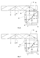
- FIGS. 37 to 39 are, respectively, top, side and three-isometric views of an optical device for collimating and coupling-in input light-waves from a display light source into a substrate, in accordance with the present invention
- FIG. 40 is a schematic diagram illustrating an optical device for collimating input light-waves from a display light source into a substrate, wherein the collimating optical device and the substrate are fabricated from different optical materials, in accordance with the present invention
- FIG. 41 is a schematic diagram illustrating the distortion effect when the collimating optical device and the substrate are fabricated from different optical materials
- FIG. 42 is a schematic diagram illustrating a system for compensating for the chromatic aberration of an optical system which is fabricated from two different materials, in accordance with the present invention.
- FIG. 43 is a schematic diagram illustrating a system for compensating for the distortion of an optical system which is fabricated from two different materials, in accordance with the present invention.
- FIG. 44 is a three-dimensional schematic diagram illustrating a system for compensating for the chromatic aberration of an optical system which is fabricated from two different materials, in accordance with the present invention.
- FIG. 45 is a schematic diagram illustrating the chromatic aberration when a central trapped light-wave is coupled out from the substrate at an output direction which deviates with respect to the normal of the major plane of the substrate;
- FIG. 46 is a schematic diagram illustrating distortion when a central trapped light-wave is coupled out from the substrate at an output direction which deviates with respect to the normal of the major plane of the substrate;
- FIG. 47 is a schematic diagram illustrating a system for compensating for the chromatic aberration of an optical system when the output direction deviates with respect to the normal of the major plane of the substrate, in accordance with the present invention
- FIG. 48 is a schematic diagram illustrating an optical device for compensating for the distortion of an optical system when the output direction deviates with respect to the normal of the major plane of the substrate, in accordance with the present invention
- FIG. 49 is a schematic diagram illustrating a device for collimating input light-waves from a display light source into an substrate, by utilizing a telephoto system, in accordance with the present invention
- FIG. 50 is a schematic diagram illustrating an optical device having a focusing lens, in accordance with the present invention.
- FIG. 51 is a schematic diagram illustrating an optical system having a unity magnification telescope, in accordance with the present invention.
- FIG. 52 is a schematic diagram illustrating an optical system having a unity magnification telescope, including an inverting prism in accordance with the present invention.
- the light-waves are coupled-out of the substrate through an external surface 12 of the light-guide 6 .
- the light-waves then pass through a quarter-wavelength retardation plate 14 , reflected by a reflecting optical element 16 , e.g., a flat mirror, return to pass again through the retardation plate 14 , and re-enter the light-guide 6 through external surface 12 .
- the now p-polarized light-waves pass through the polarizing beamsplitter 10 and are coupled out of the light-guide through an external surface 18 of the light-guide 6 .
- the light-waves then pass through a second quarter-wavelength retardation plate 20 , collimated by a component 22 , e.g., a lens, at its reflecting surface 24 , return to pass again through the retardation plate 20 , and re-enter the light-guide 6 through external surface 18 .
- the now s-polarized light-waves reflect-off the polarizing beamsplitter 10 and exit the light-guide through the exit surface 26 .
- the reflecting surfaces 16 and 24 can be materialized either by a metallic or by a dielectric coating.
- FIG. 2 illustrates how a LCCD 28 constituted by the components detailed with respect to FIG. 1 , can be combined with a substrate 30 , to form an optical system.
- a substrate 30 typically includes at least two major surfaces 32 and 34 and edges, one or more partially reflecting surface 36 and an optical element 38 for coupling light thereinto.
- the output light-waves 40 from the LCCD 28 enter the substrate 30 through its lower surface 32 .
- the incoming light-waves (vis-a-vis the substrate 30 ) are reflected from optical element 38 and trapped in the substrate as illustrated in FIG. 2 .
- the LCCD 28 comprising the display light source 4 , the folding prisms 42 and 44 , the polarizing beamsplitter 10 , the retardation plates 14 and 20 and the reflecting optical element 16 and reflecting collimating component 22 , can easily be integrated into a single mechanical module which can be assembled independently of the substrate, with fairly relaxed mechanical tolerances.
- the retardation plates 14 and 20 and the reflecting optical elements 16 and 22 could be cemented together respectively to form single elements.
- other methods could be used to combine these into a single element, such as laminating a quarter-wavelength film onto the front surface of the reflecting optical element 16 and reflecting collimating component 22 .
- all the optical elements of the LCCD 28 apart from the display light source 4 , could be cemented together to form a single optical module.
- the display light source it is usually required to keep an air gap between the LCCD and the display light source, in order to enable a focusing mechanism, however, there are systems wherein the required focal distance of the LCCD is known.
- the optical waves should be collimated by the LCCD to infinity.
- the focal depth of the collimating component is large enough to accommodate the various fabrication and assembly tolerances of the LCCD, then it is possible to locate the display light source 4 with regard to the LCCD 28 at a pre-defined distance. In that case, the display source could be attached, e.g., cemented, to the LCCD 28 utilizing an intermediate transparent plate 46 ( FIG. 3 ), having a thickness according to the required focal distance of the LCCD.
- FIG. 3 illustrates such a module wherein the exit surface 26 of the LCCD 28 is cemented, at the interface plane 48 , to the lower surface 32 of the substrate 30 .
- the main problem of this configuration is that the attaching procedure cancels the previously existing air gap 50 (illustrated in FIG. 2 ) between the substrate 30 and the LCCD 28 .
- This air gap is essential for trapping the input lightwaves 40 inside the substrate 30 . As illustrated in FIG. 3 , the trapped light-waves 40 should be reflected at points 52 and 54 of the interface plane 48 .
- a reflecting coating should be applied at this plane, either at the major surface 32 of the substrate 30 or at the exit surface 26 of the LCCD 28 .
- a simple reflecting coating cannot, however, be easily applied, since these surfaces should also be transparent to the light-waves that enter and exit the substrate 30 at the exemplary points 56 .
- the light-waves should pass through plane 48 at small incident angles, and reflect at higher incident angles. In the example illustrated, the passing incident angles are between 0° and 15° and the reflecting incident angles are between 47° and 80°.
- FIGS. 4 and 5 illustrate, for s- and p-polarization respectively, the reflectance curves as functions of the incident angles for three representative wavelengths in the photopic region: 460 nm, 550 nm and 640 nm.
- FIG. 4 it is possible to achieve the required behavior of high reflectance (above 95%) at large incident angles and low reflectance (below 5%) at small incident angles, for s-polarized light-waves.
- For p-polarized light-waves however, as illustrated in FIG. 5 , it is impossible to achieve high reflectance at incident angles between 50° and 70°, due to the proximity to the Brewster angle.
- the light-waves from the display light source, as well as the reflected light-waves of the coupling mirror 38 , which impinge on the points 52 and 54 , are s-polarized and the required reflectance could be achieved.
- the light-waves from the display light source are linearly p-polarized and the major axis of the grid is rotated by 90°, compared to that of FIGS. 1 and 2 , i.e., the polarizing beamsplitter is oriented here to reflect the p-polarization and transmit the s-polarization.
- FIG. 6 illustrates a device wherein a half-wavelength retardation plate 58 is disposed between the upper surface 26 of the LCCD 28 and the exit surface 32 of the substrate 30 .
- a half-wavelength retardation plate 58 is disposed between the upper surface 26 of the LCCD 28 and the exit surface 32 of the substrate 30 .
- a difficulty still existing in the configurations of FIGS. 3 and 6 is that the substrate 30 and the LCCD 28 , are assembled from several different components. Since the fabrication process usually involves cementing optical elements, and since the required angular-sensitive reflecting coating 27 is applied to the surface of the light-guide 6 only after the bodies of the substrate 30 and the LCCD 28 are complete, it is not possible to utilize the conventional hot-coating procedures that may damage the cemented areas. Novel thin-film technologies, as well as ion-assisted coating procedures, can also be used for cold processing. Eliminating the need to heat parts, allows cemented parts to be coated safely.
- FIG. 7 An alternative structure of a device is illustrated in FIG. 7 .
- transparent plate 60 is placed at the interface plane 48 .
- the required coating can simply be applied to the upper surface of this light-guide, which is adjacent to the substrate 30 , utilizing conventional hot-coating procedures and then cementing it at the proper place.
- the optical path inside the LCCD 28 from the display light source 4 to the reflecting surface 24 of the component 22 is the required focal length of the collimating component.
- this can be achieved by controlling the lateral dimensions of the LCCD 28 , however, there are systems, particularly for eyeglasses systems, where it is desired to minimize the lateral dimension between surface 12 and surface 18 of the LCCD 28 . That is, to reduce the width of the LCCD 28 at the expense of increasing the distance between the display light source and the substrate 30 .
- the lateral dimensions of the folding prism could be reduced, as long as the entire FOV of the image can be coupled into the LCCD with no vignetting. In that case, however, the optical path between the display light source 4 and the collimating component 22 is reduced, and therefore, the output light-waves from the LCCD 28 are no longer collimated.
- a blank plate 62 is placed between the display light source 4 and the lower prism 42 of the LCCD 28 .
- the plate 62 is optically cemented to the lower prism 42 at the interface plane 64 .
- the marginal waves 66 and 68 are collimated by the LCCD 28 to the exit pupil 70 , without any obstruction.
- the planar reflecting surface 16 (of FIG. 1 ) is replaced by a second converging lens 72 .
- the light-waves that pass through the quarter-wavelength retardation plate 14 of FIG. 1 are partially collimated by collimating component 72 , e.g., a lens, at its reflecting surface 74 .
- the partially collimated light-waves return to pass again through the retardation plate 14 , and re-enter the light-guide 6 through surface 12 .
- the now p-polarized light-waves pass through the polarizing beamsplitter 10 and are coupled-out of the light-guide through surface 18 of the light-guide.
- the light-waves then pass through the second quarter-wavelength retardation plate 20 , and are completely collimated by the component 22 at its reflecting surface 24 .
- Another benefit of utilizing two collimating components in the LCCD 28 is that the required focal length can be achieved with a shorter optical path between the display source and the output surface of the LCCD 28 , by exploiting an appropriate telephoto design.
- FIG. 10 illustrates an optical device with two converging collimating components 22 and 72 , wherein it is not necessary to utilize the blank plate 62 (of FIG. 8 ). This device is shorter than the one shown in FIG. 8 as well as narrower than the one which shown in FIG. 1 .
- LCOS light source panels contain a two-dimensional array of cells filled with liquid crystals that twist and align in response to control voltages. With the LCOS light source, however, the cells are grafted directly onto a reflective silicon chip. As the liquid crystals twist, the polarization of the light is either changed or unchanged following reflection of the mirrored surface below. This, together with a polarizing beamsplitter, causes modulation of the light-waves and creates the image.
- the reflective technology means the illumination and imaging light beams share the same space.
- FIG. 11 illustrates a cubic polarizing beamsplitter 80 inserted instead of a simple blank plate between the display light source and the LCCD 28 .
- the p-polarized light-waves 82 emanating from a light source 84 , reflect-off the polarizing beamsplitter 86 and illuminate the front surface of the LCOS light source 88 .
- the polarization of the reflected light-waves from the “light” pixels is rotated to the s-polarization and the light-waves are then passed through the beamsplitter 86 and enter the prism 42 through the lower surface 8 .
- the light-waves are then collimated as described above with reference to FIG. 1 . If the light-waves source 84 is unpolarized, it is possible to add a polarizer 90 , which transmits only the desired polarization.
- the LCCD 28 remains compact and retains its narrow form.
- FIG. 12 A modified embodiment of FIG. 11 , wherein a longer optical pathway inside the LCCD is required, is illustrated in FIG. 12 .
- the p-polarized light-waves 82 emanating from a light source 84 , pass through the polarizing beamsplitter 86 and illuminate the front surface of the LCOS light source 88 .
- the polarization of the reflected light-waves from the “light” pixels is rotated to the s-polarization state.
- the polarizing beamsplitter 86 the light-waves are coupled-out of the light-guide 80 through the lower surface 92 of the light-guide.
- the light-waves then pass through a quarter-wavelength retardation plate 94 , reflected by a reflecting optical element 96 , return to pass again through the retardation plate 94 , and re-enter the light-guide 80 through the lower surface 92 .
- the now p-polarized light-waves pass through the polarizing beamsplitter 86 , and enter the upper prism 42 through the lower surface 8 .
- the light-waves are then collimated, as described above with reference to FIG. 1 .
- the coupled light-waves 82 into the prism 42 be s-polarized as previously, it is possible to add a half-wavelength retardation plate 98 between prisms 80 and 42 , which rotates the light-waves into the desired polarization.
- the reflecting surfaces 16 and 96 could be replaced by converging optical components, as explained above with reference to FIG. 9 .
- the optical path is folded around the y-axis, i.e., in the x-z plane.
- the x and y axes refer to the horizontal and vertical axes of the image.
- the vertical dimension of the input aperture of the substrate, vis-à-vis the vertical output aperture of the LCCD is considerably larger than the horizontal dimension of the aperture.
- it is preferred to fold the optical pathway in prism 42 which is adjacent to the substrate, around the y-axis, as is illustrated indeed in these Figures.
- the situation is usually the opposite, i.e., the horizontal dimension is larger than the vertical one in a ratio of 4:3 for VGA format and in a ratio of 16:9 for HDTV format. It is therefore preferred to fold the optical pathway in the prism 80 , which is adjacent to the display source, around the x-axis.
- FIG. 13 A modified embodiment of FIG. 11 , wherein the folding of the optical pathway is performed in two different planes, is illustrated in FIG. 13 .
- the folding-in prism 80 is performed in the y-z plane, while in prism 42 it is performed in the x-z plane.
- the light 82 coupled into the prism 80 which is p-polarized compared to the beamsplitter 86 will be s-polarized compared to the folding beamsplitter 10 , and no rotating half-wavelength retardation plate is required between prisms 80 and 42 .
- the longer dimension of the LCCD be oriented along the handle of the eyeglasses, i.e., normal to the major surfaces of the substrate, as illustrated in the preceding figures.
- the longer dimension of the LCCD will be oriented parallel to the major surfaces of the substrate.
- the s-polarized light-waves 82 emanating from a light source 84 , are reflected-off the first polarizing beamsplitter 86 and illuminate the front surface of the LCOS light source 88 .
- the polarization of the reflected light-waves from the “light” pixels is rotated to the p-polarization state.
- the light-waves are coupled-out of the prism 100 through the lower surface 92 of the prism.
- the light-waves then pass through a quarter-wavelength retardation plate 94 , reflect by a reflecting element 96 , return to pass again through the retardation plate 94 , and re-enter the prism 100 through the lower surface 92 .
- the now s-polarized light-waves are coupled-out of the prism 100 through the lower surface 92 of the prism.
- the light-waves then pass through a second quarter-wavelength retardation plate 104 , collimated by a component 106 at its reflecting surface 108 , return to pass again through the retardation plate 104 , and re-enter the prism 100 through the lower surface 92 .
- the now-p-polarized light-waves pass through the polarizing beam-splitter 102 and exit the LCCD through the upper surface 110 to enter the substrate 30 . If it is required that the coupled light-waves 82 into the substrate 30 be s-polarized as previously, it is possible to add a half-wavelength retardation plate 58 between the upper surface 110 of the LCCD 80 and the lower surface 32 of the substrate 30 , which rotates the light-waves into the desired polarization.
- FIG. 15 A modified embodiment of FIG. 14 , wherein the two beamsplitters are oriented parallel to each other, is illustrated in FIG. 15 .
- a parallelepiped 112 connects the two beamsplitters 86 and 102 .
- the LCOS light source 88 is not located on the same side of the LCCD as the substrate 30 , but on the other side. This modification is required for systems where it is not allowed to locate the PCB of the LCOS light source near the substrate, due to assembly considerations.
- the display source plane is oriented parallel to the major surfaces of the substrate.
- FIG. 16 illustrates a modified LCCD 114 containing two embedded polarizing beamsplitters 116 and 118 , two quarter-wavelength retardation plates 120 and 122 , two reflecting surfaces 124 and 126 and a converging lens 128 .
- the s-polarized input light-wave 130 from the display source 132 reflects off the first reflecting surface 124 .
- the light-waves are reflected off the first beamsplitter 116 and are coupled out. It is then reflected and changed to p-polarized light by the retardation plate 120 and the second reflecting surface 126 .
- the light-waves are reflected, collimated and changed back to s-polarized light by the retardation plate 122 and the converging lens 128 .
- the light-waves are then reflected off the second polarizing beamsplitter 118 and exit the LCCD through the upper surface 136 .
- the incoming light-waves are now trapped into the substrate 30 in the same manner as illustrated in FIG. 2 .
- the illumination will be changed by adding a complementary prism 138 with an embedded polarizing beamsplitter 139 (instead of the reflecting surface 124 of FIG. 16 ), and a front illumination module 140 .
- the coupling-in of the light-waves into the substrate is performed utilizing a reflecting surface 38 embedded in the substrate.
- This coupling-in method suffers from a few major drawbacks. Firstly, since the reflecting surface 38 and the partially reflecting surfaces 36 are oriented at different angles, the fabrication process of the substrate having an internally embedded reflecting mirror 38 , is rather complicated.
- the distance l ( FIG. 2 ) between the input and the output apertures of the substrate, which are set by the coupled-in mirror 38 and the coupled-out surfaces 36 respectively, is determined by the fabrication process of the substrate. It is therefore not possible to control the distance l for a given substrate and for many applications it is required to keep l as a flexible parameter.
- the distance l depends on the size and the shape of the viewer's head and on the particular model of the eyeglasses frame. It is therefore advantageous to have the ability to set l during the assembly process, since otherwise, it is required to manufacture the substrates with a large variety of sizes in order to accommodate all the required possibilities. As a result, a simpler coupling-in configuration is preferred as compared to that which is illustrated hereinabove.
- FIG. 18 illustrates a span of rays that are intended to be coupled into the substrate with a minimal required input aperture.
- the points on the boundary line 146 between the edge of input aperture 148 and the lower surface 150 of the substrate 30 should be illuminated for each one of the input light-waves by two different rays that enter the substrate from two different locations: one ray 152 a that illuminates the boundary line 146 directly, and another ray 152 b , which is first reflected by the upper surface 154 before illuminating the boundary line.
- the size of the input aperture is usually determined by two marginal rays: the rightmost ray 156 b of the highest angle of the FOV and the leftmost ray 158 a of the lowest angle of the FOV.
- FIG. 19 The simplest way to couple these rays into the substrate is illustrated in FIG. 19 .
- the principal axis 160 of the LCCD 28 is oriented at the required off-axis angle ⁇ compared to the major plane of the substrate.
- a relay prism 162 is located between the LCCD 28 and the substrate 30 and is optically cemented to the lower surface 32 of the substrate such that the light from the display source is trapped inside the substrate by total internal reflection.
- the overall shape and size of this module conforms to most of the relevant applications.
- the optical component for coupling light-waves into the substrate is no longer a part of the substrate, but rather a part of the LCCD. Specifically, since the light-waves are reflected from the polarizing beamsplitter 10 directly into the substrate at an oblique angle which couples the light-waves inside the substrate by total internal reflection, it can be related to as the coupling-in element.
- the off-axis angle of the span of rays that are intended to be coupled into the substrate are set by rotating the LCCD module.
- an alternative coupling-in mechanism should replace the input mirror 38 .
- the lower surface 168 of a coupling-in prism 170 is optically cemented to the substrate 30 at the upper surface 154 of the substrate.
- the collimated light-waves from the collimating optical device (not shown) pass through the substrate 30 and the prism 170 and are then reflected from the reflecting surface 172 . After passing again through the prism 170 the light-waves are coupled into the substrate by total internal reflection.
- the collimating optical device not shown
- the points on the boundary line 176 between the lower surface 168 of the prism 170 and the upper surface 154 of the substrate 30 should be illuminated for each one of the input light-waves by two different rays that enter the substrate from two different locations: one ray 152 a first passes through prism 170 and is reflected by the reflecting surface 172 , from there it illuminates the boundary line 176 . Another ray 152 b , is first reflected by the reflecting surface 172 and then by the lower surface 150 of the substrate 30 before illuminating the boundary line. To avoid undesired reflections from the left surface 174 it can be coated by an opaque obstructive layer.
- a substrate can be utilized with the embodiments directed to the eyeglasses configuration.
- the simplest option is to use a single element for one eye.
- Another option is to use an element and a display source for each eye, projecting the same image, wherein the preferred place for the LCCD modules is next to the temples.
- a similar option is to project the same image for both eyes but utilize only one LCCD which is located between the two glasses, whereby its output is split between the two substrates.
- it is possible to project two different parts of the same image with some overlap between the two eyes, enabling a wider FOV.
- Yet another possibility is to project two different scenes, one directed to each eye, in order to create a stereoscopic image. With this alternative, attractive implementations are possible, including three-dimensional movies, advanced virtual reality, training systems, and the like.
- FIG. 21 An embodiment of a double-image arrangement, containing a single display light source 180 , two LCCDs 182 R and 182 L, two coupling-in prisms 184 R and 184 L and two substrates 30 R and 30 L is illustrated in FIG. 21 .
- the collimating of the right light-waves by the LCCD 182 R and the coupling in by the prism 184 R into the substrate 30 R is similar to that illustrated above with reference to FIGS. 2 and 20 , respectively.
- the main difference in the LCCD 182 R is that instead of utilizing a simple reflecting mirror, a half-reflecting beamsplitter 186 is localized between the LCCDs 182 R and 182 L.
- the light-waves which partially pass through the beamsplitter 186 changed to p-polarized light by passing through two quarter wave retardation plates 188 R and 188 L, which are positioned between the beamsplitter 186 and LCCDs 182 R and 182 L, respectively.
- the p-polarized light passes through the polarizing beamsplitter 190 L.
- the light-waves are then reflected, collimated and changed back to s-polarized light by the retardation plate 192 L and converging lens 194 L.
- the light-waves are reflected and changed back to p-polarized light by the retardation plate 196 and the reflecting surface 198 .
- the light-waves then pass through the polarizing beamsplitter 190 L and exit the substrate through the upper surface 200 L.
- the incoming waves could be trapped into the substrate in the same manner as that illustrated in FIG. 20 .
- the polarization of images 202 L and 202 R which are formed by the LCCDs 182 L and 182 R are p and s, respectively, which might be a shortcoming for systems where a similar polarization is required from both images.
- a half-wavelength retardation plate 204 is inserted between the left LCCD 182 L and the left substrate 30 L to form two identical linearly s-polarized images, 206 L and 206 R, which are projected into the viewer's eyes 208 L and 208 R, respectively.
- the optical pathways between the display source 180 and the reflecting surfaces of the converging lenses 194 L and 194 R, as well as the focal lengths of these lenses, should be identical.
- the parity of the number of reflections in the two LCCDs 182 L and 182 R should be equal. As seen in FIG. 21 , the number of reflections is four and two in the LCCDs 182 L and 182 R respectively, and the required identical parity is achieved.
- This optical arrangement could be assembled inside a spectacles frame, to form an optical device, wherein the same image is projected for both eyes 208 L and 208 R by utilizing only one display light source 180 located between the two glasses.
- the nose-bridge of a conventional spectacles frame is located a few millimeters above the eyes.
- FIG. 22 illustrates how to properly insert the images into the eyes of the user.
- the center of the display light source 180 is located above the centers of the eyes 208 L and 208 R.
- the coupling-in prisms 184 L and 184 R are rotated to a geometry wherein the reflecting mirrors of the prisms 184 L and 184 R are oriented parallel to the partially reflecting surfaces 36 L and 36 R, respectively.
- the projections of the central light-waves 210 L and 210 R on the substrate planes are parallel to the major axes of the substrates 212 L and 212 R, respectively, and the image light-waves are coupled into the substrate where the major axes of the images are inclined a few degrees above the horizon.
- the partially reflecting surfaces 36 L and 36 R reflect the coupled images back to their original directions and the central image light-waves are again parallel to the horizon.
- the optical module which can be added to any conventional frame, can be very compact and lightweight, with no disturbance to the user.
- FIGS. 21 and 22 a single display source is utilized. As a result, only a system having identical images for both eyes can be materialized using this embodiment.
- the light-waves from the display sources 214 L and 214 R are coupled into an intermediate prism 216 through surfaces 218 L and 218 R, respectively.
- the light-waves are then collimated by the LCCDs 220 R and 220 L and trapped inside the substrates 30 R and 30 L, respectively in a similar manner to that described above with reference to FIG. 20 .
- a similar structure is illustrated in FIG.
- the display sources 214 L and 214 R are coupled into the substrates 30 L and 30 R, respectively.
- the display sources are located at the same level as the viewer's eyes, where the space 224 between the LCCDs 220 L and 220 R is preserved for the upper part of the nose.
- FIGS. 23 and 24 are capable of projecting stereoscopic images, as well as have a wider FOV, by utilizing two different display sources.
- the necessity to use two different display sources increases the volume, the power consumption, as well as the fabrication costs of the optical system.
- An alternative manner, utilizing only a single display source while still preserving the advantages of the embodiments of FIGS. 23 and 24 is described in FIG. 25 .
- only a single display source is located next to surface 218 L and a beamsplitter 226 is inserted into the intermediate prism 216 .
- a dynamic half-wavelength retardation plate 228 is inserted between display source 214 and surface 218 L, and a polarizing beamsplitter 226 is inserted into the prism 216 .
- the display source 214 synchronized with the retardation plate 228 , operates at a double rate compared to the usual.
- an image which is designated to the left eye emanates from the display source.
- the dynamic retardation plate is switched to the off position and the s-polarized light-waves are reflected off the polarizing beamsplitter 226 , collimated by the LCCD 220 L, and coupled into the left substrate 30 L.
- an image which is designated to the right eye emanates from the display source.
- the dynamic retardation plate 228 is switched to the on position, the polarization of the light-waves is rotated to the p-state and now the p-polarized light-waves pass through the polarizing beamsplitter 226 , collimated by the LCCD 220 R and coupled into the right substrate 30 R.
- the images which are projected into the viewer's eyes can now either be identical, stereoscopic, two different parts of the same image with some overlap between the two eyes, or any desired combination.
- the polarizing beamsplitters totally reflect one polarization and totally transmit the other one.
- the operation of the beamsplitter is not perfect and there is cross-talk between the two states.
- a small fraction of the s-polarized light-waves pass through the beamsplitter and a small fraction of the p-polarized light-waves are reflected off the beamsplitter.
- these two light-waves are s-polarized, they cannot be separated utilizing a polarization sensitive element.
- the undesired light-waves 230 will be projected into the viewer's eye and a ghost image interfering with the original image, will be created.
- FIG. 27 A possible way to overcome this problem is illustrated in FIG. 27 .
- two different polarizing beamsplitters, 234 and 236 , and a linear polarizer 238 which is oriented to block s-polarized light are disposed into the LCCD 28 .
- the s-polarized light-waves 240 which pass through the first polarizing beamsplitter 234 are blocked by the polarizer 238 .
- the light-waves which are reflected as intended by the first polarizing beamsplitter are changed to p-polarized light by the retardation plate 14 and the reflecting surface 16 .
- the light-waves are then reflected, collimated and changed back to s-polarized light by the retardation plate 20 and the optical element 22 .
- the light-waves exit the substrate properly collimated through the upper surface 26 . While the configuration illustrated in FIG. 27 solves the ghost image problem, the necessity to embed two different polarizing beamsplitters and a linear polarizer inside the LCCD complicates the fabrication process of the optical module.
- the polarizing beamsplitter is oriented at an angle of 45° in relation to the major surfaces of the LCCD, and that the main output direction from the LCCD (namely, the direction of the principal ray of the central light-wave) is identical (as in FIG. 1 ) or normal to (as in FIG. 17 ) the main input direction on the LCCD.
- FIG. 28 An alternative manner for separating between the real and the ghost images by utilizing a different angle is illustrated in FIG. 28 . Accordingly, the angle between the lower surface 8 of the LCCD and the beam-splitter 10 is set to be 45°+ ⁇ , wherein a positive angular rotation is defined to be counterclockwise.
- the principal ray 242 from the light-wave 2 is rotated by the beamsplitter 10 to the angle 90°+2 ⁇ and is reflected to the angle 270° ⁇ 2 ⁇ by the reflecting surface 16 .
- the main axis of the collimating optical element 22 is oriented collinear with the incoming principal ray 244 .
- the ray is reflected back by the lens to the angle 90° ⁇ 2 ⁇ .
- the second reflection off the beamsplitter 10 yields the final direction of the principal ray to be 4 ⁇ .
- the output direction of the principal ray 244 is substantially different than the input direction of the ray. Therefore, the real and the ghost images can now be angularly separated.
- FIG. 29 A slightly modified embodiment is illustrated in FIG. 29 where, in addition to the rotation of the beamsplitter 10 , the reflecting surface 16 is rotated at an angle of ⁇ compared to its original orientation. As a result, the direction of the output central ray from the LCCD is now 4 ⁇ +2 ⁇ .
- FIG. 30 Another example, which is related to the embodiment of FIG. 15 , is illustrated in FIG. 30 .
- the angle between the incoming surface 246 and the first polarizing beamsplitter is 45°+ ⁇ and the angle between the reflecting surface 250 and the output surface 252 is ⁇ . Therefore, the output direction from the LCCD of the principal ray 253 is substantially different than the normal to the input direction of that ray 253 from the LCCD. As a result, the angle between the ghost and the real images is 2 ⁇ .
- polarizing beamsplitters There are various types of polarizing beamsplitters.
- One type contains a layer of film. This type cannot be utilized in an imaging system because the surface quality of the film is usually not sufficient for imaging of s-polarized light that is reflected off of it.
- p-polarized light that passes through the film preserves the quality of the image, and therefore, this beamsplitter can be used for illuminating the light display source.
- the beamsplitter cannot have a dual function of illumination as well as the imaging functions, such as beamsplitter 248 shown in FIG. 30 .
- the s-polarized light-waves 258 emanating from a light source 260 , are reflected off the first polarizing beamsplitter 262 and illuminate the front surface of the LCOS light source 264 .
- the polarization of the reflected light from the “light” pixels is rotated to the p-polarization state.
- the p-polarized light then passes through the polarizing beamsplitter 262 and the light-waves pass through a half wave retarder 266 and are rotated to s-polarized light.
- the light is then reflected off of the second beamsplitter 268 and is coupled out of the prism 270 through the lower surface 272 of the prism.
- the light-waves then pass through a quarter-wavelength retardation plate 274 , reflected by a reflecting optical element 276 , return to pass again through the retardation plate 274 , and re-enter the prism 270 through the lower surface 272 .
- the now p-polarized light passes through the second polarizing beamsplitter 268 and is coupled out of prism 278 through the upper surface 280 of the prism.
- the light-waves then pass through a second quarter-wavelength retardation plate 282 , collimated by a lens 283 at its reflecting surface 284 , return to pass again through the retardation plate 282 , and re-enter prism 278 through surface 280 .
- the now s-polarized light-waves are reflected off the polarizing beamsplitter 268 and exit the substrate through the upper surface 285 to enter the substrate 286 such that the light from the display source is trapped inside the substrate by total internal reflection.
- FIG. 33 An additional configuration meeting the requirement of the beamsplitter having a single function of illuminating the display source is described in FIG. 33 .
- the s-polarized light-waves 288 emanating from a light source 290 , are reflected off the first polarizing beamsplitter 292 and illuminate the front surface of the LCOS light source 294 .
- the polarization of the reflected light from the “light” pixels is rotated to the p-polarization state.
- the p-polarized light then passes through the polarizing beamsplitter 292 and the light-waves pass through a half wave retarder 295 and are rotated to s-polarized light.
- the light is then reflected off the first reflecting surface 296 and follows total internal reflection off the lower surface 298 of the prism 300 .
- the light-waves are then reflected off the polarizing beamsplitter 302 and are coupled out through the lower surface 298 of the prism. They pass through a quarter-wavelength retardation plate 304 , are collimated by a lens 306 at its reflecting surface 308 , return to pass again through the retardation plate 304 , and re-enter prism 300 through the lower surface 298 .
- the now p-polarized light-waves pass through the polarizing beamsplitter 302 and exit the substrate through the upper surface 310 .
- the s-polarized light that is reflected off the beamsplitter is reflected before the light impinges the display source, and hence, the first beamsplitter is not limited to a certain type, as opposed to the second beamsplitter, which is limited to a type which preserves the quality of the image.
- FIGS. 28 to 31 An additional advantage illustrated in FIGS. 28 to 31 is that it is possible to differentiate between the mechanical orientation of the LCCD and the direction of the output wave. There are cases where it is required to rotate the mechanical axis of the LCCD while still retaining the on-axis impinging angle on the substrate.
- the angle between the lower surface 8 and the beamsplitter 10 is set to ⁇ 45° ⁇ .
- the angle between the input and the output light-waves of the LCCD is ⁇ 4 ⁇ . Therefore, the mechanical angle between the major axis of the LCCD and the normal to the substrate, is ⁇ 4 ⁇ while the central output wave from the LCCD vis-à-vis the central input light-wave of the substrate impinges normal to the major surface of the substrate, as required.
- FIG. 35 illustrates another example based on the embodiment which is described above with reference to FIG. 19 .
- the angle between surface 8 and the beamsplitter 10 is 52.5°. Therefore, while the mechanical axis of the LCCD is oriented at an angle of 30° to normal of the major surfaces of the substrate, the central incoming wave is oriented at the required off-axis angle of 60°.
- a cubic polarizing beamsplitter 316 is inserted between the display source and the LCCD.
- the s-polarized light-waves 314 emanating from a light source 84 , reflect off the polarizing beamsplitter 312 of a prism 316 and illuminate the front surface of the LCOS light source 318 .
- the polarization of the reflected light from the “light” pixels is rotated to the p-polarization and the light-waves are then passed through the beamsplitter 312 and enter the prism 320 through the lower surface 8 .
- the light-waves are then collimated as described above with reference to FIG. 35 .
- the coupled light 314 into the prism 320 will be s-polarized as in the folding beamsplitter 316 , and it is possible to add a half-wavelength retardation plate 322 between prisms 316 and 320 , which rotates the light into the desired polarization.
- the optical path is folded around the y axis, that is, in the x-z plane, wherein the x and y axes are referred to the horizontal and vertical axes of the image.
- the horizontal dimension is larger than the vertical one in a ratio of 4:3 for VGA format and in a ratio of 16:9 for HDTV format. Therefore, it is preferred to fold the optical pathway in the prism 316 , which is adjacent to the display source, around the x axis.
- FIGS. 37 top view
- 38 side view
- 39 three-dimensional view
- the folding-in prism 316 folds the light in the y-z plane by the polarizing beamsplitter, while in prism 320 it is folded in the x-z plane.
- the light 314 coupled into the prism 320 which is p-polarized compared to the beamsplitter 312 , will be s-polarized compared to the folding beamsplitter 320 , and no rotating half-wavelength retardation plate is required between prisms 316 and 320 .
- the LCCD and the substrate are fabricated from the same optical material.
- the differences in the optical properties of the two elements should not cause any particular problem.
- the central light-wave intersects the interface plane between the LCCD and the substrate normal to the plane.
- the direction of the incoming light-wave will not be influenced by the optical difference between the two elements.
- the intersection angle of the interface plane will be fairly small and the undesired effects will be negligible.
- the central wave intersects the interface plane between the LCCD and the substrate at a highly oblique angle which is larger than the critical angle for total internal reflection inside the substrate.
- undesired effects may appear which may severely degrade the optical performance of these systems.
- a ray 324 from the central wave of the image source impinges on the interface surface 326 between the LCCD and the substrate at an off-axis angle ⁇ in .
- the LCCD and the substrate have been fabricated of different optical materials having refractive indices and Abbe values of n 1 ; v i and n 2 ; v 2 , respectively.
- the input light-wave is a continuum of wavelengths over the entire photopic spectrum, but for the simplicity of the illustration only three representative wavelengths: ⁇ r ; ⁇ g and ⁇ b have been considered.
- the off-axis angle ⁇ ′ in of coupled ray inside the substrate is given by:
- n 2 /n 1 is usually not uniform for the entire photopic spectrum, that is:
- FIG. 41 Another undesired effect is illustrated in FIG. 41 .
- the central point of the image source and the two marginal points, which are at the same distance from the central point, are represented by the three rays, 334 , 336 and 338 , respectively.
- the two marginal rays are equally angularly deviated from the central ray, i.e., the incoming angles of the three rays 334 , 336 and 338 on the interface plane 326 are ⁇ in , ⁇ in ⁇ and ⁇ in + ⁇ , respectively.
- the angular deviation ⁇ in between the incoming ray and the coupled ray inside the substrate is given by:
- the intermediate prism 340 between the LCCD and the substrate is fabricated of an optical material having a refractive index and an Abbe value of n 3 and v 3 , respectively.
- the prism 340 which is practically a part of the LCCD 28 , can be fabricated of an optical material, which is similar to that of the substrate 30 .
- the interface plane 342 between the prism 340 and the LCCD is slanted at an angle ⁇ nt in respect to the interface plane 326 between the substrate and the prism. Now, the incoming rays intersect two interface planes before being coupled into the substrate.
- FIG. 44 is a three-dimensional illustration of a system where the display source is an LCOS light source which is illuminated by the same method as described above with reference to FIGS. 37 to 39 . Since the interface between the LCCD and the substrate in FIG. 44 is identical to that of an LCD-based system, the design procedure should be also similar here.
- FIG. 45 Another situation where a combination of an LCCD and a substrate can yield an optical system which suffers chromatic aberration, as well as distortion, is illustrated in FIG. 45 .
- the input light-waves are coupled into the LCCD normal to the input surface 344 , the central light-wave is reflected off of the partially reflective surfaces 36 of the substrate at an output direction which is significantly deviated at an angle ⁇ ′ out in respect to the normal of the substrate's plane.
- the refractive index and the Abbe value of the substrate are n 2 and v 2 and that the light-waves are coupled out from the substrate into the air
- An example for an optical system where the output light-waves are significantly oblique to the substrate plane is in a case where it is required that the projected image will not block the central angular area of the viewer. In that case, it is preferred to project the image from the peripheral part of the substrate.
- n 2 is usually not uniform for the entire photopic spectrum, that is: n 2 ( ⁇ r ) ⁇ n 2 ( ⁇ g ) ⁇ n 2 ( ⁇ b ) (10) and consequentially: sin ⁇ out ( ⁇ r ) ⁇ sin ⁇ out ( ⁇ g ) ⁇ sin ⁇ out ( ⁇ b ) (11) That is, the single incoming ray 346 is divided outside the substrate into three different rays 348 , 350 and 352 outside the substrate for the three different wavelengths ⁇ r , ⁇ g and ⁇ b , respectively. As a result, the output light-waves which are coupled out of the substrate are smeared as a function of the wavelength, and the image quality will suffer from a severe chromatic aberration.
- the central point of the image source and the two marginal points which are at an equal distance from the central point are represented by the three rays, 354 , 356 and 358 , respectively.
- the two marginal rays are equally angularly deviated from the central ray. That is, the off-axis angles of the three rays 354 , 356 and 358 after the reflection from the partially reflection surfaces 36 are ⁇ ′ out , ⁇ ′ out ⁇ and ⁇ ′ out + ⁇ , respectively.
- Eq the derivation of Eq.
- an intermediate prism 340 which is fabricated of an optical material having a refractive index and Abbe value of n 3 and v 3 , respectively, is inserted between the LCCD and the substrate, wherein the interface plane 342 between the prism 340 and the LCCD is slanted at an angle ⁇ int with respect to the interface plane 326 which is located between the substrate and the prism. It is assumed that in the most general case where the LCCD and the substrate are fabricated of the optical materials, where the refractive indices and Abbe values are n 1 ; v 1 and n 2 ; v 2 , respectively.
- the central white ray 346 is refracted by the first interface plane 342 into three different rays 348 , 350 and 352 which have three different wavelengths ⁇ r , ⁇ g and ⁇ b , respectively.
- Each ray is, however, refracted differently by the two other interface planes, 326 and 32 , in such a way that all these three rays are coupled-out of the substrate at the same off-axis angle.
- the chromatic aberration of the image ray 346 is essentially eliminated.
- FIG. 48 illustrates the combination of the distortion effects of all three interface planes.
- the central point of the image source and the two marginal points which are represented by the three rays 354 , 356 and 358 , respectively, are equally angularly deviated after the collimation by the LCCD.
- Each of these rays is differently deviated by the three interface planes, but the combination of all the three different deviations yields a total deviation which is fairly uniform for the different image light-waves.
- the total distortion of the optical system is significantly improved as compared to that of FIG. 46 , wherein only one interface plane contributes to the distortion.
- the s-polarized light-waves 360 emanating from a light display source 362 , are reflected off the first polarizing beamsplitter 364 and are coupled-out of the prism 366 through surface 368 of the prism.
- the light-waves then pass through a quarter-wavelength retardation plate 370 , reflected by a first reflecting optical element 372 , return to pass again through the retardation plate 370 , and re-enter the prism 366 through surface 368 .
- the now p-polarized light-waves pass through the polarizing beamsplitter 364 and are coupled out of prism 366 through surface 374 of the prism.
- the light-waves then pass through a second quarter-wavelength retardation plate 376 , diverged by a concave lens 378 at its reflecting surface 380 , return to pass again through the retardation plate 376 , and re-enter prism 366 through surface 374 .
- the now s-polarized light-waves are reflected off the polarizing beamsplitter 364 and exit prism 366 through the upper surface 382 to enter the second prism 384 through its lower surface 386 .
- the light-waves are then reflected off the second polarizing beamsplitter 388 and are coupled out of the prism 384 through surface 390 .
- the light-waves then pass through a third quarter-wavelength retardation plate 392 , reflected by a second reflecting optical element 394 , return to pass again through the retardation plate 398 , and re-enter prism 384 through surface 390 .
- the now p-polarized light-waves pass through the second polarizing beamsplitter 388 and are coupled-out of prism 384 through surface 396 .
- the light-waves then pass through a fourth quarter-wavelength retardation plate 398 , collimated by a convex lens 400 at its reflecting surface 402 , return to pass again through the retardation plate 398 , and re-enter prism 384 through surface 396 .
- the now s-polarized light-waves are reflected off the second polarizing beamsplitter 388 and exit the substrate through the upper surface 404 to enter the substrate 30 .
- the LCCD operates as a collimator, namely, a real image from a display light source is focused to infinity.
- the main purpose for materializing the LCCD is to create collimated light-waves as the input for a substrate-based optical system.
- an LCCD could be utilized for different optical operations and many other applications, i.e., the LCCD can focus an image to a different distance than infinity and can be inserted into other systems where it is desired to achieve a satisfactory performance and retain a compact and light-weight system.
- FIG. 50 illustrates an optical system where the LCCD serves as a focusing lens for a camera.
- the p-polarized component of the input wave 406 from an external scene passes through the upper surface 407 of the LCCD 408 and through the polarizing beamsplitter 410 . It is then reflected, converged and changed to s-polarized light by the retardation plate 412 and a focusing lens 414 having a reflective back surface 416 . Following a reflection off the polarizing beamsplitter 410 , it is reflected and changed to p-polarized light by the retardation plate 417 and a reflecting surface 418 .
- the converging light-waves exit the LCCD through the left surface 420 and are then focused onto a detector plane 422 .
- a focus mechanism might be added to this device by enabling a lateral translation of the camera or of the focusing lens along the z-axis in relation to the lower plane 424 .
- FIG. 51 Another potential embodiment is illustrated in FIG. 51 .
- a converging LCCD 426 and a collimating LCCD 428 are combined together to form a unity magnification telescope.
- An optical filter 430 can be inserted into the Fourier plane, in order to perform any required image processing.
- an energy-sensitive filter can be inserted to block high-intensity signals.
- the main drawback of the system illustrated in FIG. 51 is that the image is vertically inverted, i.e., the transferred image appears upside-down to the viewer's eye.
- FIG. 52 illustrates a modified system wherein an inverting prism 432 is added at the input surface 434 of the unity magnification telescope.
- an inverting prism 432 is added at the input surface 434 of the unity magnification telescope.
- the image will appear at the proper orientation to the viewer's eye.
- Different LCCDs can be combined to form magnifying or de-magnifying systems.
- the telescope can be combined with a substrate, in order to project a processed or a magnified image from the external view to a viewer's eye.
Applications Claiming Priority (5)
| Application Number | Priority Date | Filing Date | Title |
|---|---|---|---|
| IL182705A IL182705A (en) | 2007-04-22 | 2007-04-22 | Compact optical component in conductive substrate |
| IL182705 | 2007-04-22 | ||
| IL190881A IL190881A0 (en) | 2008-04-15 | 2008-04-15 | Compact imaging lens in a substrate |
| IL190881 | 2008-04-15 | ||
| PCT/IL2008/000523 WO2008129539A2 (en) | 2007-04-22 | 2008-04-17 | A collimating optical device and system |
Related Parent Applications (1)
| Application Number | Title | Priority Date | Filing Date |
|---|---|---|---|
| PCT/IL2008/000523 A-371-Of-International WO2008129539A2 (en) | 2007-04-22 | 2008-04-17 | A collimating optical device and system |
Related Child Applications (8)
| Application Number | Title | Priority Date | Filing Date |
|---|---|---|---|
| US14/148,970 Continuation US8902503B2 (en) | 2007-04-22 | 2014-01-07 | Collimating optical device and system |
| US14/148,998 Continuation US9104036B2 (en) | 2007-04-22 | 2014-01-07 | Collimating optical device and system |
| US14/149,049 Continuation US8810914B2 (en) | 2007-04-22 | 2014-01-07 | Collimating optical device and system |
| US14/149,036 Division US9448408B2 (en) | 2007-04-22 | 2014-01-07 | Collimating optical device and system |
| US14/148,987 Continuation US9069180B2 (en) | 2007-04-22 | 2014-01-07 | Collimating optical device and system |
| US14/149,058 Continuation US9417453B2 (en) | 2007-04-22 | 2014-01-07 | Collimating optical device and system |
| US14/149,012 Continuation US8861081B2 (en) | 2007-04-22 | 2014-01-07 | Collimating optical device and system |
| US14/149,023 Continuation US9316832B2 (en) | 2007-04-22 | 2014-01-07 | Collimating optical device and system |
Publications (2)
| Publication Number | Publication Date |
|---|---|
| US20100202048A1 US20100202048A1 (en) | 2010-08-12 |
| US8643948B2 true US8643948B2 (en) | 2014-02-04 |
Family
ID=39684348
Family Applications (14)
| Application Number | Title | Priority Date | Filing Date |
|---|---|---|---|
| US12/596,823 Active 2029-09-27 US8643948B2 (en) | 2007-04-22 | 2008-04-17 | Collimating optical device and system |
| US14/149,036 Active US9448408B2 (en) | 2007-04-22 | 2014-01-07 | Collimating optical device and system |
| US14/148,970 Active US8902503B2 (en) | 2007-04-22 | 2014-01-07 | Collimating optical device and system |
| US14/149,058 Active US9417453B2 (en) | 2007-04-22 | 2014-01-07 | Collimating optical device and system |
| US14/149,012 Active US8861081B2 (en) | 2007-04-22 | 2014-01-07 | Collimating optical device and system |
| US14/149,023 Active US9316832B2 (en) | 2007-04-22 | 2014-01-07 | Collimating optical device and system |
| US14/148,987 Active US9069180B2 (en) | 2007-04-22 | 2014-01-07 | Collimating optical device and system |
| US14/148,998 Active US9104036B2 (en) | 2007-04-22 | 2014-01-07 | Collimating optical device and system |
| US14/149,049 Active US8810914B2 (en) | 2007-04-22 | 2014-01-07 | Collimating optical device and system |
| US14/738,377 Active US9207457B2 (en) | 2007-04-22 | 2015-06-12 | Collimating optical device and system |
| US14/738,412 Active US9279986B2 (en) | 2007-04-22 | 2015-06-12 | Collimating optical device and system |
| US15/062,943 Active US9500869B2 (en) | 2007-04-22 | 2016-03-07 | Collimating optical device and system |
| US15/067,524 Active US9513481B2 (en) | 2007-04-22 | 2016-03-11 | Collimating optical device and system |
| US15/234,700 Active 2028-05-07 US9740013B2 (en) | 2007-04-22 | 2016-08-11 | Collimating optical device and system |
Family Applications After (13)
| Application Number | Title | Priority Date | Filing Date |
|---|---|---|---|
| US14/149,036 Active US9448408B2 (en) | 2007-04-22 | 2014-01-07 | Collimating optical device and system |
| US14/148,970 Active US8902503B2 (en) | 2007-04-22 | 2014-01-07 | Collimating optical device and system |
| US14/149,058 Active US9417453B2 (en) | 2007-04-22 | 2014-01-07 | Collimating optical device and system |
| US14/149,012 Active US8861081B2 (en) | 2007-04-22 | 2014-01-07 | Collimating optical device and system |
| US14/149,023 Active US9316832B2 (en) | 2007-04-22 | 2014-01-07 | Collimating optical device and system |
| US14/148,987 Active US9069180B2 (en) | 2007-04-22 | 2014-01-07 | Collimating optical device and system |
| US14/148,998 Active US9104036B2 (en) | 2007-04-22 | 2014-01-07 | Collimating optical device and system |
| US14/149,049 Active US8810914B2 (en) | 2007-04-22 | 2014-01-07 | Collimating optical device and system |
| US14/738,377 Active US9207457B2 (en) | 2007-04-22 | 2015-06-12 | Collimating optical device and system |
| US14/738,412 Active US9279986B2 (en) | 2007-04-22 | 2015-06-12 | Collimating optical device and system |
| US15/062,943 Active US9500869B2 (en) | 2007-04-22 | 2016-03-07 | Collimating optical device and system |
| US15/067,524 Active US9513481B2 (en) | 2007-04-22 | 2016-03-11 | Collimating optical device and system |
| US15/234,700 Active 2028-05-07 US9740013B2 (en) | 2007-04-22 | 2016-08-11 | Collimating optical device and system |
Country Status (3)
| Country | Link |
|---|---|
| US (14) | US8643948B2 (de) |
| EP (1) | EP2142953B1 (de) |
| WO (1) | WO2008129539A2 (de) |
Cited By (74)
| Publication number | Priority date | Publication date | Assignee | Title |
|---|---|---|---|---|
| US20080278812A1 (en) * | 2005-11-08 | 2008-11-13 | Lumus Ltd. | Polarizing Optical System |
| US20100073579A1 (en) * | 2008-09-25 | 2010-03-25 | Kabushiki Kaisha Toshiba | Optical member, display device using the optical member and movable body using the display device |
| US20140118813A1 (en) * | 2007-04-22 | 2014-05-01 | Lumus Ltd | Collimating optical device and system |
| US20160357024A1 (en) * | 2015-02-05 | 2016-12-08 | Boe Technology Group Co., Ltd. | 3d display glasses |
| US9519092B1 (en) * | 2012-03-21 | 2016-12-13 | Google Inc. | Display method |
| US20160377868A1 (en) * | 2014-03-18 | 2016-12-29 | 3M Innovative Properties Company | Low profile image combiner for near-eye displays |
| US20170052379A1 (en) * | 2015-08-18 | 2017-02-23 | Quanta Computer Inc. | See-through head-mounted display |
| US20170235144A1 (en) * | 2014-07-15 | 2017-08-17 | Samsung Electronics Co., Ltd. | Holographic see-through optical device, stereoscopic imaging system, and multimedia head mounted system |
| US20170285346A1 (en) * | 2016-03-30 | 2017-10-05 | Coretronic Corporation | Optical waveguide device and head-mounted display apparatus using the same |
| US9915823B1 (en) | 2014-05-06 | 2018-03-13 | Google Llc | Lightguide optical combiner for head wearable display |
| US10048499B2 (en) | 2005-11-08 | 2018-08-14 | Lumus Ltd. | Polarizing optical system |
| US10089516B2 (en) | 2013-07-31 | 2018-10-02 | Digilens, Inc. | Method and apparatus for contact image sensing |
| US10145533B2 (en) | 2005-11-11 | 2018-12-04 | Digilens, Inc. | Compact holographic illumination device |
| US10156681B2 (en) | 2015-02-12 | 2018-12-18 | Digilens Inc. | Waveguide grating device |
| US10185154B2 (en) | 2011-04-07 | 2019-01-22 | Digilens, Inc. | Laser despeckler based on angular diversity |
| US10209517B2 (en) | 2013-05-20 | 2019-02-19 | Digilens, Inc. | Holographic waveguide eye tracker |
| US10216061B2 (en) | 2012-01-06 | 2019-02-26 | Digilens, Inc. | Contact image sensor using switchable bragg gratings |
| US10234696B2 (en) | 2007-07-26 | 2019-03-19 | Digilens, Inc. | Optical apparatus for recording a holographic device and method of recording |
| US10241330B2 (en) | 2014-09-19 | 2019-03-26 | Digilens, Inc. | Method and apparatus for generating input images for holographic waveguide displays |
| US10302835B2 (en) | 2017-02-22 | 2019-05-28 | Lumus Ltd. | Light guide optical assembly |
| US10330777B2 (en) | 2015-01-20 | 2019-06-25 | Digilens Inc. | Holographic waveguide lidar |
| US10359736B2 (en) | 2014-08-08 | 2019-07-23 | Digilens Inc. | Method for holographic mastering and replication |
| US10409144B2 (en) | 2009-10-09 | 2019-09-10 | Digilens Inc. | Diffractive waveguide providing structured illumination for object detection |
| US10423222B2 (en) | 2014-09-26 | 2019-09-24 | Digilens Inc. | Holographic waveguide optical tracker |
| US10437064B2 (en) | 2015-01-12 | 2019-10-08 | Digilens Inc. | Environmentally isolated waveguide display |
| US10437068B2 (en) | 2017-02-16 | 2019-10-08 | Coretronic Corporation | Optical waveguide element and display device |
| US10437031B2 (en) | 2016-11-08 | 2019-10-08 | Lumus Ltd. | Light-guide device with optical cutoff edge and corresponding production methods |
| US10437051B2 (en) | 2012-05-11 | 2019-10-08 | Digilens Inc. | Apparatus for eye tracking |
| US10459145B2 (en) | 2015-03-16 | 2019-10-29 | Digilens Inc. | Waveguide device incorporating a light pipe |
| US10481319B2 (en) | 2017-03-22 | 2019-11-19 | Lumus Ltd. | Overlapping facets |
| US10520731B2 (en) | 2014-11-11 | 2019-12-31 | Lumus Ltd. | Compact head-mounted display system protected by a hyperfine structure |
| US10545346B2 (en) | 2017-01-05 | 2020-01-28 | Digilens Inc. | Wearable heads up displays |
| US10551544B2 (en) | 2018-01-21 | 2020-02-04 | Lumus Ltd. | Light-guide optical element with multiple-axis internal aperture expansion |
| US10564417B2 (en) | 2016-10-09 | 2020-02-18 | Lumus Ltd. | Aperture multiplier using a rectangular waveguide |
| US10591756B2 (en) | 2015-03-31 | 2020-03-17 | Digilens Inc. | Method and apparatus for contact image sensing |
| US10642058B2 (en) | 2011-08-24 | 2020-05-05 | Digilens Inc. | Wearable data display |
| US10649214B2 (en) | 2005-02-10 | 2020-05-12 | Lumus Ltd. | Substrate-guide optical device |
| US10670876B2 (en) | 2011-08-24 | 2020-06-02 | Digilens Inc. | Waveguide laser illuminator incorporating a despeckler |
| US10678053B2 (en) | 2009-04-27 | 2020-06-09 | Digilens Inc. | Diffractive projection apparatus |
| US10690916B2 (en) | 2015-10-05 | 2020-06-23 | Digilens Inc. | Apparatus for providing waveguide displays with two-dimensional pupil expansion |
| US10690851B2 (en) | 2018-03-16 | 2020-06-23 | Digilens Inc. | Holographic waveguides incorporating birefringence control and methods for their fabrication |
| WO2020130505A1 (en) * | 2018-12-18 | 2020-06-25 | Samsung Electronics Co., Ltd. | Apparatus and method of displaying image and computer program thereof |
| US10732569B2 (en) | 2018-01-08 | 2020-08-04 | Digilens Inc. | Systems and methods for high-throughput recording of holographic gratings in waveguide cells |
| US10739512B2 (en) * | 2018-09-09 | 2020-08-11 | Lumus Ltd. | Optical systems including light-guide optical elements with two-dimensional expansion |
| US10809528B2 (en) | 2014-04-23 | 2020-10-20 | Lumus Ltd. | Compact head-mounted display system |
| US20200371311A1 (en) * | 2017-12-03 | 2020-11-26 | Lumus Ltd. | Optical device alignment methods |
| US10859768B2 (en) | 2016-03-24 | 2020-12-08 | Digilens Inc. | Method and apparatus for providing a polarization selective holographic waveguide device |
| US10890707B2 (en) | 2016-04-11 | 2021-01-12 | Digilens Inc. | Holographic waveguide apparatus for structured light projection |
| US10895679B2 (en) | 2017-04-06 | 2021-01-19 | Lumus Ltd. | Light-guide optical element and method of its manufacture |
| CN112243076A (zh) * | 2019-07-19 | 2021-01-19 | 宏达国际电子股份有限公司 | 电子装置 |
| US10914950B2 (en) | 2018-01-08 | 2021-02-09 | Digilens Inc. | Waveguide architectures and related methods of manufacturing |
| US10942430B2 (en) | 2017-10-16 | 2021-03-09 | Digilens Inc. | Systems and methods for multiplying the image resolution of a pixelated display |
| US10983340B2 (en) | 2016-02-04 | 2021-04-20 | Digilens Inc. | Holographic waveguide optical tracker |
| US11092810B2 (en) | 2017-11-21 | 2021-08-17 | Lumus Ltd. | Optical aperture expansion arrangement for near-eye displays |
| US11204540B2 (en) | 2009-10-09 | 2021-12-21 | Digilens Inc. | Diffractive waveguide providing a retinal image |
| US11243434B2 (en) | 2017-07-19 | 2022-02-08 | Lumus Ltd. | LCOS illumination via LOE |
| US11307432B2 (en) | 2014-08-08 | 2022-04-19 | Digilens Inc. | Waveguide laser illuminator incorporating a Despeckler |
| US11378732B2 (en) | 2019-03-12 | 2022-07-05 | DigLens Inc. | Holographic waveguide backlight and related methods of manufacturing |
| US11385465B2 (en) * | 2017-08-24 | 2022-07-12 | tooz technologies GmbH | Curved light guide, imaging optical unit and HMD |
| US11402801B2 (en) | 2018-07-25 | 2022-08-02 | Digilens Inc. | Systems and methods for fabricating a multilayer optical structure |
| US11415812B2 (en) | 2018-06-26 | 2022-08-16 | Lumus Ltd. | Compact collimating optical device and system |
| US11442222B2 (en) | 2019-08-29 | 2022-09-13 | Digilens Inc. | Evacuated gratings and methods of manufacturing |
| US11448937B2 (en) | 2012-11-16 | 2022-09-20 | Digilens Inc. | Transparent waveguide display for tiling a display having plural optical powers using overlapping and offset FOV tiles |
| US11448816B2 (en) | 2019-01-24 | 2022-09-20 | Lumus Ltd. | Optical systems including light-guide optical elements with two-dimensional expansion |
| US11460621B2 (en) | 2012-04-25 | 2022-10-04 | Rockwell Collins, Inc. | Holographic wide angle display |
| US11480788B2 (en) | 2015-01-12 | 2022-10-25 | Digilens Inc. | Light field displays incorporating holographic waveguides |
| US11513350B2 (en) | 2016-12-02 | 2022-11-29 | Digilens Inc. | Waveguide device with uniform output illumination |
| US11523092B2 (en) | 2019-12-08 | 2022-12-06 | Lumus Ltd. | Optical systems with compact image projector |
| US11543594B2 (en) | 2019-02-15 | 2023-01-03 | Digilens Inc. | Methods and apparatuses for providing a holographic waveguide display using integrated gratings |
| US11681143B2 (en) | 2019-07-29 | 2023-06-20 | Digilens Inc. | Methods and apparatus for multiplying the image resolution and field-of-view of a pixelated display |
| US11726332B2 (en) | 2009-04-27 | 2023-08-15 | Digilens Inc. | Diffractive projection apparatus |
| US11747568B2 (en) | 2019-06-07 | 2023-09-05 | Digilens Inc. | Waveguides incorporating transmissive and reflective gratings and related methods of manufacturing |
| US11796729B2 (en) | 2021-02-25 | 2023-10-24 | Lumus Ltd. | Optical aperture multipliers having a rectangular waveguide |
| EP4339656A2 (de) | 2018-05-14 | 2024-03-20 | Lumus Ltd. | Projektorkonfiguration mit unterteilter optischer apertur für augennahe anzeigen und entsprechende optische systeme |
Families Citing this family (121)
| Publication number | Priority date | Publication date | Assignee | Title |
|---|---|---|---|---|
| IL166799A (en) | 2005-02-10 | 2014-09-30 | Lumus Ltd | Aluminum shale surfaces for use in a conductive substrate |
| US8279499B2 (en) * | 2010-05-10 | 2012-10-02 | Xerox Corporation | Single LED dual light guide |
| US9160906B2 (en) | 2011-02-03 | 2015-10-13 | Jason R. Bond | Head-mounted face image capturing devices and systems |
| US8573866B2 (en) | 2011-02-03 | 2013-11-05 | Jason R. Bond | Head-mounted face image capturing devices and systems |
| FR2982376B1 (fr) * | 2011-11-07 | 2014-01-03 | Laster | Dispositif portable de vision augmentee. |
| US9001030B2 (en) * | 2012-02-15 | 2015-04-07 | Google Inc. | Heads up display |
| US9239415B2 (en) | 2012-03-08 | 2016-01-19 | Google Inc. | Near-to-eye display with an integrated out-looking camera |
| US8749886B2 (en) * | 2012-03-21 | 2014-06-10 | Google Inc. | Wide-angle wide band polarizing beam splitter |
| KR102095330B1 (ko) | 2012-04-05 | 2020-03-31 | 매직 립, 인코포레이티드 | 능동 포비에이션 능력을 갖는 와이드-fov(field of view) 이미지 디바이스들 |
| IL219907A (en) | 2012-05-21 | 2017-08-31 | Lumus Ltd | Integrated head display system with eye tracking |
| US9658453B1 (en) | 2013-04-29 | 2017-05-23 | Google Inc. | Head-mounted display including diffractive combiner to integrate a display and a sensor |
| US9128285B2 (en) * | 2013-04-30 | 2015-09-08 | Google Inc. | Head-mounted display including integrated projector |
| CA2913482C (en) | 2013-05-27 | 2018-05-15 | Huawei Technologies Co., Ltd. | Filter, method for producing filter, and laser wavelength monitoring apparatus |
| FR3010193A1 (fr) * | 2013-08-29 | 2015-03-06 | Sunpartner | Dispositif optique concentrateur de la lumiere ambiante |
| US10146055B2 (en) | 2013-09-06 | 2018-12-04 | 3M Innovative Properties Company | Head mounted display with eye tracking |
| JP2015102796A (ja) * | 2013-11-27 | 2015-06-04 | セイコーエプソン株式会社 | 光分岐装置 |
| KR20150085224A (ko) * | 2014-01-15 | 2015-07-23 | 코닝정밀소재 주식회사 | 기판의 에지부 검사장치 |
| CN108572449B (zh) * | 2014-03-31 | 2021-09-14 | 联想(北京)有限公司 | 显示装置和电子设备 |
| WO2015157016A1 (en) * | 2014-04-09 | 2015-10-15 | 3M Innovative Properties Company | Head mounted display and low conspicuity pupil illuminator |
| CN105093536B (zh) * | 2014-05-06 | 2018-07-06 | 联想(北京)有限公司 | 显示设备和电子设备 |
| KR102216405B1 (ko) * | 2014-05-30 | 2021-02-16 | 엘지전자 주식회사 | 광학장치 및 이를 구비하는 영상투사장치 |
| EP3149939A4 (de) * | 2014-05-30 | 2018-02-21 | Magic Leap, Inc. | Verfahren und systeme zur anzeige von stereoskopie mit einem optischen freiformsystem mit adressierbarem fokus für virtuelle und erweiterte realität |
| CN105445935B (zh) * | 2014-06-26 | 2017-12-29 | 联想(北京)有限公司 | 显示装置和电子设备 |
| RU2579804C1 (ru) * | 2014-09-16 | 2016-04-10 | Самсунг Электроникс Ко., Лтд. | Оптическое устройство для формирования изображений дополненной реальности |
| KR20160059406A (ko) * | 2014-11-18 | 2016-05-26 | 삼성전자주식회사 | 가상 이미지를 출력하기 위한 웨어러블 장치 및 방법 |
| CN107111149A (zh) * | 2014-12-01 | 2017-08-29 | Sn合伙合同会社 | 空中像显示装置 |
| DE102014119550B4 (de) * | 2014-12-23 | 2022-05-12 | tooz technologies GmbH | Abbildungsoptik zum Erzeugen eines virtuellen Bildes und Datenbrille |
| IL236490B (en) * | 2014-12-25 | 2021-10-31 | Lumus Ltd | Optical component on a conductive substrate |
| EP3243099B1 (de) * | 2015-01-06 | 2020-08-12 | Vuzix Corporation | Am kopf montierte bildgebungsvorrichtung mit optischer kopplung |
| CN104656258B (zh) * | 2015-02-05 | 2017-06-16 | 上海理湃光晶技术有限公司 | 屈光度可调的曲面波导近眼光学显示器件 |
| IL237337B (en) | 2015-02-19 | 2020-03-31 | Amitai Yaakov | A compact head-up display system with a uniform image |
| US10088689B2 (en) * | 2015-03-13 | 2018-10-02 | Microsoft Technology Licensing, Llc | Light engine with lenticular microlenslet arrays |
| WO2016204433A1 (en) * | 2015-06-15 | 2016-12-22 | Samsung Electronics Co., Ltd. | Head mounted display apparatus |
| KR20160147636A (ko) * | 2015-06-15 | 2016-12-23 | 삼성전자주식회사 | 헤드 마운티드 디스플레이 장치 |
| US10067352B2 (en) * | 2015-06-15 | 2018-09-04 | Robert Joe Alderman | 3D image generating lens tool |
| US10967566B2 (en) * | 2015-10-30 | 2021-04-06 | Seurat Technologies, Inc. | Chamber systems for additive manufacturing |
| FR3046850B1 (fr) * | 2016-01-15 | 2018-01-26 | Universite De Strasbourg | Guide optique ameliore et systeme optique comportant un tel guide optique |
| WO2017127494A1 (en) | 2016-01-22 | 2017-07-27 | Corning Incorporated | Wide field personal display |
| US10459230B2 (en) * | 2016-02-02 | 2019-10-29 | Disney Enterprises, Inc. | Compact augmented reality / virtual reality display |
| IL244177B (en) * | 2016-02-18 | 2021-04-29 | Oorym Optics Ltd | A display system with a uniform image |
| CN105589202A (zh) | 2016-03-18 | 2016-05-18 | 京东方科技集团股份有限公司 | 一种显示装置、显示方法和显示系统 |
| US10704903B2 (en) * | 2016-03-22 | 2020-07-07 | Sintai Optical (Shenzhen) Co., Ltd. | Binocular capable of measuring distance and prism and light transmitter module thereof |
| CN107219621B (zh) * | 2016-03-22 | 2019-10-29 | 信泰光学(深圳)有限公司 | 可测距的双筒望远镜及其棱镜模块 |
| US9897811B2 (en) * | 2016-04-07 | 2018-02-20 | Google Llc | Curved eyepiece with color correction for head wearable display |
| US10215986B2 (en) * | 2016-05-16 | 2019-02-26 | Microsoft Technology Licensing, Llc | Wedges for light transformation |
| WO2017199232A1 (en) | 2016-05-18 | 2017-11-23 | Lumus Ltd. | Head-mounted imaging device |
| US10353202B2 (en) * | 2016-06-09 | 2019-07-16 | Microsoft Technology Licensing, Llc | Wrapped waveguide with large field of view |
| US9996984B2 (en) | 2016-07-05 | 2018-06-12 | Disney Enterprises, Inc. | Focus control for virtual objects in augmented reality (AR) and virtual reality (VR) displays |
| CN106226901B (zh) * | 2016-08-31 | 2019-05-21 | 深圳超多维科技有限公司 | 一种光学器件及头戴式显示装置 |
| US10976155B2 (en) | 2016-09-27 | 2021-04-13 | Intuitive Surgical Operations, Inc. | Micro optic assemblies and optical interrogation systems |
| US10466479B2 (en) | 2016-10-07 | 2019-11-05 | Coretronic Corporation | Head-mounted display apparatus and optical system |
| JP6857384B2 (ja) * | 2016-11-24 | 2021-04-14 | 国立大学法人大阪大学 | 光学素子 |
| CN208953803U (zh) | 2016-12-02 | 2019-06-07 | 鲁姆斯有限公司 | 具紧凑型准直图像投影仪的光学系统 |
| US10725301B2 (en) * | 2016-12-08 | 2020-07-28 | Darwin Hu | Method and apparatus for transporting optical images |
| US20190162967A1 (en) * | 2016-12-08 | 2019-05-30 | Darwin Hu | Light weight display glasses using an active optical cable |
| US10409066B2 (en) | 2017-01-19 | 2019-09-10 | Coretronic Corporation | Head-mounted display device with waveguide elements |
| EP3574360A4 (de) | 2017-01-28 | 2020-11-11 | Lumus Ltd. | Bildgebungssystem mit erweiterter realität |
| US10955668B2 (en) * | 2017-02-14 | 2021-03-23 | Optecks, Llc | Optical display system for augmented reality and virtual reality |
| JP2018146950A (ja) * | 2017-03-02 | 2018-09-20 | 株式会社リコー | 表示装置及び機器 |
| CN108873326A (zh) | 2017-05-16 | 2018-11-23 | 中强光电股份有限公司 | 头戴式显示装置 |
| US10560688B2 (en) | 2017-05-22 | 2020-02-11 | Microsoft Technology Licensing, Llc | Display device system with non-telecentric imaging to prevent ghost images |
| JP2018205448A (ja) * | 2017-05-31 | 2018-12-27 | セイコーエプソン株式会社 | 表示装置及び照明装置 |
| US10976551B2 (en) | 2017-08-30 | 2021-04-13 | Corning Incorporated | Wide field personal display device |
| CN107450188A (zh) * | 2017-08-31 | 2017-12-08 | 深圳珑璟光电技术有限公司 | 一种3d近眼显示装置及方法 |
| CN109581657A (zh) * | 2017-09-28 | 2019-04-05 | 弗莱克斯有限公司 | 波导和dlp光引擎的光学耦合 |
| WO2019064301A1 (en) | 2017-09-29 | 2019-04-04 | Lumus Ltd. | DISPLAY WITH INCREASED REALITY |
| CN107621700B (zh) * | 2017-10-11 | 2019-04-16 | 北京亮亮视野科技有限公司 | 平板波导 |
| KR20200077511A (ko) | 2017-10-22 | 2020-06-30 | 루머스 리미티드 | 광학 벤치를 사용하는 헤드 장착형 증강 현실 장치 |
| WO2019106636A1 (en) | 2017-12-03 | 2019-06-06 | Lumus Ltd. | Optical device testing method and apparatus |
| KR102568792B1 (ko) | 2017-12-04 | 2023-08-21 | 삼성전자주식회사 | 회절 광학 렌즈를 구비한 다중 영상 디스플레이 장치 |
| CN107870438B (zh) | 2017-12-04 | 2019-11-22 | 华为技术有限公司 | 增强现实的装置、光引擎部件和方法 |
| CN109946907A (zh) | 2017-12-20 | 2019-06-28 | 中强光电股份有限公司 | 投影装置 |
| JP2019113721A (ja) | 2017-12-25 | 2019-07-11 | セイコーエプソン株式会社 | 導光装置及び表示装置 |
| CN107966819A (zh) * | 2017-12-27 | 2018-04-27 | 北京灵犀微光科技有限公司 | 波导显示装置 |
| IL275615B (en) | 2018-01-02 | 2022-08-01 | Lumus Ltd | Augmented reality representatives with active alignment and matching methods |
| US10506220B2 (en) | 2018-01-02 | 2019-12-10 | Lumus Ltd. | Augmented reality displays with active alignment and corresponding methods |
| JP7389491B2 (ja) | 2018-04-08 | 2023-11-30 | ルムス エルティーディー. | 光学サンプルの特性評価 |
| EP3794397A4 (de) | 2018-05-17 | 2021-07-07 | Lumus Ltd. | Augennahe anzeige mit überlappenden projektoranordnungen |
| CN110515202B (zh) * | 2018-05-21 | 2022-01-28 | 北京亮亮视野科技有限公司 | 光导显示系统 |
| IL259518B2 (en) | 2018-05-22 | 2023-04-01 | Lumus Ltd | Optical system and method for improving light field uniformity |
| MX2020012512A (es) | 2018-05-23 | 2021-02-16 | Lumus Ltd | Sistema optico que incluye elemento optico de guia de luz con superficies internas parcialmente reflejantes. |
| CN108761789B (zh) * | 2018-05-24 | 2020-03-10 | 京东方科技集团股份有限公司 | 抬头显示器及汽车 |
| JP3222489U (ja) * | 2018-05-27 | 2019-08-01 | ルムス エルティーディー. | 像面湾曲の影響を緩和した基板誘導ベースの光学系 |
| CN110286486B (zh) * | 2018-06-03 | 2021-08-20 | 胡大文 | 用于输送光学图像的方法 |
| CN112313499A (zh) | 2018-06-21 | 2021-02-02 | 鲁姆斯有限公司 | 光导光学元件(loe)的板之间折射率不均匀性的测量技术 |
| KR20200001863A (ko) * | 2018-06-28 | 2020-01-07 | 삼성전자주식회사 | 디스플레이 장치 |
| KR20210031705A (ko) | 2018-07-16 | 2021-03-22 | 루머스 리미티드 | 편광 내부 반사기를 사용하는 광 가이드 광학 요소 |
| US10861240B1 (en) * | 2018-09-26 | 2020-12-08 | Facebook Technologies, Llc | Virtual pupil camera in head mounted display |
| CN109188695B (zh) * | 2018-09-29 | 2021-11-30 | 北京蚁视科技有限公司 | 一种薄型大视场角近眼显示装置 |
| CN109100866A (zh) * | 2018-10-22 | 2018-12-28 | 萤欧(上海)汽车科技有限公司 | 一种基于液晶偏振方向旋转器的车载ar-hud光学系统 |
| CN109188700B (zh) * | 2018-10-30 | 2021-05-11 | 京东方科技集团股份有限公司 | 光学显示系统及ar/vr显示装置 |
| JP7436478B2 (ja) * | 2018-11-02 | 2024-02-21 | メタ プラットフォームズ テクノロジーズ, リミテッド ライアビリティ カンパニー | コンパクトな偏光ベースのマルチパス光アーキテクチャ |
| EP3867696B1 (de) | 2018-11-08 | 2022-08-03 | Lumus Ltd. | Optische vorrichtungen und systeme mit dichroitischem strahlteilerfarbkombinierer |
| TWM642752U (zh) | 2018-11-08 | 2023-06-21 | 以色列商魯姆斯有限公司 | 用於將圖像顯示到觀察者的眼睛中的顯示器 |
| TWM598414U (zh) | 2018-11-11 | 2020-07-11 | 以色列商魯姆斯有限公司 | 具有中間視窗的近眼顯示器 |
| US11849262B2 (en) | 2019-03-12 | 2023-12-19 | Lumus Ltd. | Image projector |
| EP3942349A1 (de) * | 2019-04-18 | 2022-01-26 | BAE SYSTEMS plc | Optische anordnung für eine anzeige |
| US10775626B1 (en) * | 2019-05-16 | 2020-09-15 | Rockwell Collins, Inc. | Wide field of view head worn display device |
| GB201909179D0 (en) * | 2019-06-26 | 2019-08-07 | Wave Optics Ltd | Pupil relay system |
| MX2021015750A (es) | 2019-06-27 | 2022-01-27 | Lumus Ltd | Aparato y metodos de seguimiento ocular a partir de la obtencion de imagenes oculares mediante un elemento optico de guia de luz. |
| US11269184B2 (en) | 2019-11-20 | 2022-03-08 | Coretronic Corporation | Head-mounted display device |
| US11667004B2 (en) | 2019-11-25 | 2023-06-06 | Lumus Ltd. | Method of polishing a surface of a waveguide |
| IL270991B (en) | 2019-11-27 | 2020-07-30 | Lumus Ltd | A light guide with an optical element to perform polarization mixing |
| MX2022006238A (es) | 2019-12-05 | 2022-06-22 | Lumus Ltd | Elemento optico de guia de luz que utiliza reflectores parciales complementarios recubiertos y elemento optico de guia de luz con dispersion de luz reducida. |
| US11029564B1 (en) * | 2019-12-19 | 2021-06-08 | Lumileds Llc | Polarizing edge coupled light in backlight |
| US11054654B1 (en) | 2020-03-03 | 2021-07-06 | Coretronic Corporation | Near-eye display device |
| US11119325B1 (en) | 2020-03-06 | 2021-09-14 | Coretronic Corporation | Near eye display device |
| TW202206891A (zh) * | 2020-06-01 | 2022-02-16 | 以色列商魯姆斯有限公司 | 用於近眼顯示器的虛擬影像遞送系統 |
| US11243400B1 (en) | 2020-07-17 | 2022-02-08 | Rockwell Collins, Inc. | Space suit helmet having waveguide display |
| JP7232360B2 (ja) * | 2020-08-11 | 2023-03-02 | カラーリンク・ジャパン 株式会社 | 偏光ビームスプリッタ及びディスプレイシステム |
| US20220269098A1 (en) * | 2020-08-23 | 2022-08-25 | Lumus Ltd. | Optical System |
| CN111983811B (zh) * | 2020-09-09 | 2022-08-19 | 京东方科技集团股份有限公司 | 一种近眼显示装置 |
| DE202021104723U1 (de) | 2020-09-11 | 2021-10-18 | Lumus Ltd. | An ein optisches Lichtleiterelement gekoppelter Bildprojektor |
| CN116368413A (zh) * | 2020-10-01 | 2023-06-30 | 鲁姆斯有限公司 | 复合光导光学元件 |
| IL309921A (en) | 2020-11-18 | 2024-03-01 | Lumus Ltd | Optical validation of orientations of internal surfaces |
| KR20230148324A (ko) | 2021-03-01 | 2023-10-24 | 루머스 리미티드 | 프로젝터로부터 도파관으로의 콤팩트한 커플링을 갖는광학 시스템 |
| JPWO2022249456A1 (de) * | 2021-05-28 | 2022-12-01 | ||
| US11789264B2 (en) | 2021-07-04 | 2023-10-17 | Lumus Ltd. | Display with stacked light-guide elements providing different parts of field of view |
| US11480800B1 (en) | 2021-09-13 | 2022-10-25 | Snap Inc. | Compact catadioptric projector |
| CN114236682B (zh) * | 2022-01-20 | 2022-12-09 | 上海理湃光晶技术有限公司 | 一种光学扩展波导 |
| US11662591B1 (en) * | 2022-07-01 | 2023-05-30 | Brelyon Inc. | Display systems and imaging systems with dynamically controllable optical path lengths |
Citations (16)
| Publication number | Priority date | Publication date | Assignee | Title |
|---|---|---|---|---|
| US3658405A (en) * | 1969-05-26 | 1972-04-25 | Maksvmilian Pluta | Variable phase-contrast and interference microscope |
| US3677621A (en) * | 1969-11-24 | 1972-07-18 | Vickers Ltd | Optical field flattening devices |
| GB1321303A (en) | 1970-03-31 | 1973-06-27 | Pilkington Perkin Elmer Ltd | Optical systems |
| WO1998015868A1 (en) | 1996-10-08 | 1998-04-16 | The Microoptical Corporation | Image combining system for eyeglasses and face masks |
| US6204975B1 (en) | 1998-12-22 | 2001-03-20 | Virtual Vision, Inc. | Reflective micro-display system |
| US6310713B2 (en) * | 1997-04-07 | 2001-10-30 | International Business Machines Corporation | Optical system for miniature personal displays using reflective light valves |
| WO2002088825A2 (en) | 2001-04-27 | 2002-11-07 | Koninklijke Philips Electronics N.V. | Compact display device |
| WO2002097515A1 (en) | 2001-05-26 | 2002-12-05 | Thales Optics Ltd | Optical device using a polarizing beam splitter |
| WO2003081320A1 (en) | 2002-03-21 | 2003-10-02 | Lumus Ltd. | Light guide optical device |
| EP1385023A1 (de) | 2002-07-17 | 2004-01-28 | C.R.F. Società Consortile per Azioni | Lichtleiter für eine am Kopf montierte- oder Head-up- Anzeigevorrichtung |
| US6829095B2 (en) * | 2000-06-05 | 2004-12-07 | Lumus, Ltd. | Substrate-guided optical beam expander |
| WO2006085308A1 (en) | 2005-02-10 | 2006-08-17 | Lumus Ltd. | Substrate-guide optical device utilizing polarization beam splitters |
| WO2007093983A2 (en) | 2006-02-14 | 2007-08-23 | Lumus Ltd. | Substrate-guided imaging lens |
| WO2008023367A1 (en) | 2006-08-22 | 2008-02-28 | Lumus Ltd. | Substrate-guided optical device |
| US7391573B2 (en) * | 2003-09-10 | 2008-06-24 | Lumus Ltd. | Substrate-guided optical devices |
| US20080278812A1 (en) * | 2005-11-08 | 2008-11-13 | Lumus Ltd. | Polarizing Optical System |
Family Cites Families (18)
| Publication number | Priority date | Publication date | Assignee | Title |
|---|---|---|---|---|
| US2958258A (en) * | 1953-09-21 | 1960-11-01 | Technicolor Corp | Optical projection of beam controlled object fields |
| BE758771A (fr) | 1969-11-11 | 1971-04-16 | Sandoz Sa | Composes azoiques, leur preparation et leur utilisation |
| US5537260A (en) * | 1993-01-26 | 1996-07-16 | Svg Lithography Systems, Inc. | Catadioptric optical reduction system with high numerical aperture |
| JPH08114765A (ja) * | 1994-10-15 | 1996-05-07 | Fujitsu Ltd | 偏光分離・変換素子並びにこれを用いた偏光照明装置及び投射型表示装置 |
| US6704065B1 (en) * | 1995-04-07 | 2004-03-09 | Colorlink, Inc. | Optical system for producing a modulated color image |
| US6257726B1 (en) * | 1997-02-13 | 2001-07-10 | Canon Kabushiki Kaisha | Illuminating apparatus and projecting apparatus |
| US6710927B2 (en) * | 2000-06-26 | 2004-03-23 | Angus Duncan Richards | Multi-mode display device |
| US20040218271A1 (en) * | 2001-07-18 | 2004-11-04 | Carl Zeiss Smt Ag | Retardation element made from cubic crystal and an optical system therewith |
| US6879443B2 (en) * | 2003-04-25 | 2005-04-12 | The Microoptical Corporation | Binocular viewing system |
| IL157838A (en) * | 2003-09-10 | 2013-05-30 | Yaakov Amitai | High-brightness optical device |
| CN101174028B (zh) * | 2004-03-29 | 2015-05-20 | 索尼株式会社 | 光学装置以及虚像显示装置 |
| EP1748305A4 (de) * | 2004-05-17 | 2009-01-14 | Nikon Corp | Optisches element, optisches kombinierersystem und bildanzeigeeinheit |
| IL162573A (en) * | 2004-06-17 | 2013-05-30 | Lumus Ltd | Optical component in a large key conductive substrate |
| IL163361A (en) * | 2004-08-05 | 2011-06-30 | Lumus Ltd | Optical device for light coupling into a guiding substrate |
| JP5030134B2 (ja) * | 2005-08-18 | 2012-09-19 | 株式会社リコー | 偏光変換素子、偏光変換光学系および画像投影装置 |
| WO2007062098A2 (en) * | 2005-11-21 | 2007-05-31 | Microvision, Inc. | Display with image-guiding substrate |
| JP5013407B2 (ja) | 2006-01-26 | 2012-08-29 | 株式会社アドバンテスト | レーザ発振器 |
| US8643948B2 (en) * | 2007-04-22 | 2014-02-04 | Lumus Ltd. | Collimating optical device and system |
-
2008
- 2008-04-17 US US12/596,823 patent/US8643948B2/en active Active
- 2008-04-17 WO PCT/IL2008/000523 patent/WO2008129539A2/en active Application Filing
- 2008-04-17 EP EP08738225.5A patent/EP2142953B1/de active Active
-
2014
- 2014-01-07 US US14/149,036 patent/US9448408B2/en active Active
- 2014-01-07 US US14/148,970 patent/US8902503B2/en active Active
- 2014-01-07 US US14/149,058 patent/US9417453B2/en active Active
- 2014-01-07 US US14/149,012 patent/US8861081B2/en active Active
- 2014-01-07 US US14/149,023 patent/US9316832B2/en active Active
- 2014-01-07 US US14/148,987 patent/US9069180B2/en active Active
- 2014-01-07 US US14/148,998 patent/US9104036B2/en active Active
- 2014-01-07 US US14/149,049 patent/US8810914B2/en active Active
-
2015
- 2015-06-12 US US14/738,377 patent/US9207457B2/en active Active
- 2015-06-12 US US14/738,412 patent/US9279986B2/en active Active
-
2016
- 2016-03-07 US US15/062,943 patent/US9500869B2/en active Active
- 2016-03-11 US US15/067,524 patent/US9513481B2/en active Active
- 2016-08-11 US US15/234,700 patent/US9740013B2/en active Active
Patent Citations (21)
| Publication number | Priority date | Publication date | Assignee | Title |
|---|---|---|---|---|
| US3658405A (en) * | 1969-05-26 | 1972-04-25 | Maksvmilian Pluta | Variable phase-contrast and interference microscope |
| US3677621A (en) * | 1969-11-24 | 1972-07-18 | Vickers Ltd | Optical field flattening devices |
| GB1321303A (en) | 1970-03-31 | 1973-06-27 | Pilkington Perkin Elmer Ltd | Optical systems |
| WO1998015868A1 (en) | 1996-10-08 | 1998-04-16 | The Microoptical Corporation | Image combining system for eyeglasses and face masks |
| US6310713B2 (en) * | 1997-04-07 | 2001-10-30 | International Business Machines Corporation | Optical system for miniature personal displays using reflective light valves |
| US6204975B1 (en) | 1998-12-22 | 2001-03-20 | Virtual Vision, Inc. | Reflective micro-display system |
| US6829095B2 (en) * | 2000-06-05 | 2004-12-07 | Lumus, Ltd. | Substrate-guided optical beam expander |
| WO2002088825A2 (en) | 2001-04-27 | 2002-11-07 | Koninklijke Philips Electronics N.V. | Compact display device |
| WO2002097515A1 (en) | 2001-05-26 | 2002-12-05 | Thales Optics Ltd | Optical device using a polarizing beam splitter |
| WO2003081320A1 (en) | 2002-03-21 | 2003-10-02 | Lumus Ltd. | Light guide optical device |
| EP1562066A2 (de) | 2002-03-21 | 2005-08-10 | Lumus Ltd | Optische lichtleitervorrichtung |
| US7457040B2 (en) * | 2002-03-21 | 2008-11-25 | Lumus Ltd. | Light guide optical device |
| EP1385023A1 (de) | 2002-07-17 | 2004-01-28 | C.R.F. Società Consortile per Azioni | Lichtleiter für eine am Kopf montierte- oder Head-up- Anzeigevorrichtung |
| US7391573B2 (en) * | 2003-09-10 | 2008-06-24 | Lumus Ltd. | Substrate-guided optical devices |
| US20080151379A1 (en) * | 2005-02-10 | 2008-06-26 | Lumus Ltd. | Substrate-Guide Optical Device Utilizing Polarization Beam Splitters |
| WO2006085308A1 (en) | 2005-02-10 | 2006-08-17 | Lumus Ltd. | Substrate-guide optical device utilizing polarization beam splitters |
| US20080278812A1 (en) * | 2005-11-08 | 2008-11-13 | Lumus Ltd. | Polarizing Optical System |
| WO2007093983A2 (en) | 2006-02-14 | 2007-08-23 | Lumus Ltd. | Substrate-guided imaging lens |
| US8000020B2 (en) * | 2006-02-14 | 2011-08-16 | Lumus Ltd. | Substrate-guided imaging lens |
| WO2008023367A1 (en) | 2006-08-22 | 2008-02-28 | Lumus Ltd. | Substrate-guided optical device |
| US20100067110A1 (en) * | 2006-08-22 | 2010-03-18 | Lu | Substrate-guided optical device |
Cited By (136)
| Publication number | Priority date | Publication date | Assignee | Title |
|---|---|---|---|---|
| US10962784B2 (en) | 2005-02-10 | 2021-03-30 | Lumus Ltd. | Substrate-guide optical device |
| US10649214B2 (en) | 2005-02-10 | 2020-05-12 | Lumus Ltd. | Substrate-guide optical device |
| US10598937B2 (en) | 2005-11-08 | 2020-03-24 | Lumus Ltd. | Polarizing optical system |
| US10048499B2 (en) | 2005-11-08 | 2018-08-14 | Lumus Ltd. | Polarizing optical system |
| US9551880B2 (en) * | 2005-11-08 | 2017-01-24 | Lumus Ltd. | Polarizing optical system |
| US20080278812A1 (en) * | 2005-11-08 | 2008-11-13 | Lumus Ltd. | Polarizing Optical System |
| US10261321B2 (en) | 2005-11-08 | 2019-04-16 | Lumus Ltd. | Polarizing optical system |
| US10145533B2 (en) | 2005-11-11 | 2018-12-04 | Digilens, Inc. | Compact holographic illumination device |
| US8861081B2 (en) * | 2007-04-22 | 2014-10-14 | Lumus Ltd | Collimating optical device and system |
| US9500869B2 (en) | 2007-04-22 | 2016-11-22 | Lumus Ltd. | Collimating optical device and system |
| US9207457B2 (en) | 2007-04-22 | 2015-12-08 | Lumus Ltd. | Collimating optical device and system |
| US9279986B2 (en) | 2007-04-22 | 2016-03-08 | Lumus Ltd | Collimating optical device and system |
| US9316832B2 (en) * | 2007-04-22 | 2016-04-19 | Lumus Ltd. | Collimating optical device and system |
| US9417453B2 (en) * | 2007-04-22 | 2016-08-16 | Lumus Ltd. | Collimating optical device and system |
| US9448408B2 (en) * | 2007-04-22 | 2016-09-20 | Lumus Ltd. | Collimating optical device and system |
| US9104036B2 (en) * | 2007-04-22 | 2015-08-11 | Lumus Ltd. | Collimating optical device and system |
| US9513481B2 (en) | 2007-04-22 | 2016-12-06 | Lumus Ltd. | Collimating optical device and system |
| US9069180B2 (en) * | 2007-04-22 | 2015-06-30 | Lumus Ltd | Collimating optical device and system |
| US8902503B2 (en) * | 2007-04-22 | 2014-12-02 | Lumus Ltd. | Collimating optical device and system |
| US8810914B2 (en) * | 2007-04-22 | 2014-08-19 | Lumus Ltd. | Collimating optical device and system |
| US20140126056A1 (en) * | 2007-04-22 | 2014-05-08 | Lumus Ltd. | Collimating optical device and system |
| US20140126052A1 (en) * | 2007-04-22 | 2014-05-08 | Lumus Ltd. | Collimating optical device and system |
| US20140118813A1 (en) * | 2007-04-22 | 2014-05-01 | Lumus Ltd | Collimating optical device and system |
| US9740013B2 (en) | 2007-04-22 | 2017-08-22 | Lumus Ltd. | Collimating optical device and system |
| US10725312B2 (en) | 2007-07-26 | 2020-07-28 | Digilens Inc. | Laser illumination device |
| US10234696B2 (en) | 2007-07-26 | 2019-03-19 | Digilens, Inc. | Optical apparatus for recording a holographic device and method of recording |
| US20100073579A1 (en) * | 2008-09-25 | 2010-03-25 | Kabushiki Kaisha Toshiba | Optical member, display device using the optical member and movable body using the display device |
| US10678053B2 (en) | 2009-04-27 | 2020-06-09 | Digilens Inc. | Diffractive projection apparatus |
| US11726332B2 (en) | 2009-04-27 | 2023-08-15 | Digilens Inc. | Diffractive projection apparatus |
| US11175512B2 (en) | 2009-04-27 | 2021-11-16 | Digilens Inc. | Diffractive projection apparatus |
| US10409144B2 (en) | 2009-10-09 | 2019-09-10 | Digilens Inc. | Diffractive waveguide providing structured illumination for object detection |
| US11204540B2 (en) | 2009-10-09 | 2021-12-21 | Digilens Inc. | Diffractive waveguide providing a retinal image |
| US11487131B2 (en) | 2011-04-07 | 2022-11-01 | Digilens Inc. | Laser despeckler based on angular diversity |
| US10185154B2 (en) | 2011-04-07 | 2019-01-22 | Digilens, Inc. | Laser despeckler based on angular diversity |
| US10670876B2 (en) | 2011-08-24 | 2020-06-02 | Digilens Inc. | Waveguide laser illuminator incorporating a despeckler |
| US10642058B2 (en) | 2011-08-24 | 2020-05-05 | Digilens Inc. | Wearable data display |
| US11287666B2 (en) | 2011-08-24 | 2022-03-29 | Digilens, Inc. | Wearable data display |
| US10216061B2 (en) | 2012-01-06 | 2019-02-26 | Digilens, Inc. | Contact image sensor using switchable bragg gratings |
| US10459311B2 (en) | 2012-01-06 | 2019-10-29 | Digilens Inc. | Contact image sensor using switchable Bragg gratings |
| US9519092B1 (en) * | 2012-03-21 | 2016-12-13 | Google Inc. | Display method |
| US11460621B2 (en) | 2012-04-25 | 2022-10-04 | Rockwell Collins, Inc. | Holographic wide angle display |
| US10437051B2 (en) | 2012-05-11 | 2019-10-08 | Digilens Inc. | Apparatus for eye tracking |
| US11448937B2 (en) | 2012-11-16 | 2022-09-20 | Digilens Inc. | Transparent waveguide display for tiling a display having plural optical powers using overlapping and offset FOV tiles |
| US20230114549A1 (en) * | 2012-11-16 | 2023-04-13 | Rockwell Collins, Inc. | Transparent waveguide display |
| US11815781B2 (en) * | 2012-11-16 | 2023-11-14 | Rockwell Collins, Inc. | Transparent waveguide display |
| US11662590B2 (en) | 2013-05-20 | 2023-05-30 | Digilens Inc. | Holographic waveguide eye tracker |
| US10209517B2 (en) | 2013-05-20 | 2019-02-19 | Digilens, Inc. | Holographic waveguide eye tracker |
| US10089516B2 (en) | 2013-07-31 | 2018-10-02 | Digilens, Inc. | Method and apparatus for contact image sensing |
| US10423813B2 (en) | 2013-07-31 | 2019-09-24 | Digilens Inc. | Method and apparatus for contact image sensing |
| US10345598B2 (en) | 2014-03-18 | 2019-07-09 | 3M Innovative Properties Company | Low profile image combiner for near-eye displays |
| US9977246B2 (en) * | 2014-03-18 | 2018-05-22 | 3M Innovative Properties Company | Low profile image combiner for near-eye displays |
| US20160377868A1 (en) * | 2014-03-18 | 2016-12-29 | 3M Innovative Properties Company | Low profile image combiner for near-eye displays |
| US10908426B2 (en) | 2014-04-23 | 2021-02-02 | Lumus Ltd. | Compact head-mounted display system |
| US10809528B2 (en) | 2014-04-23 | 2020-10-20 | Lumus Ltd. | Compact head-mounted display system |
| US9915823B1 (en) | 2014-05-06 | 2018-03-13 | Google Llc | Lightguide optical combiner for head wearable display |
| US10386642B2 (en) * | 2014-07-15 | 2019-08-20 | Samsung Electronics Co., Ltd. | Holographic see-through optical device, stereoscopic imaging system, and multimedia head mounted system |
| US20170235144A1 (en) * | 2014-07-15 | 2017-08-17 | Samsung Electronics Co., Ltd. | Holographic see-through optical device, stereoscopic imaging system, and multimedia head mounted system |
| US11709373B2 (en) | 2014-08-08 | 2023-07-25 | Digilens Inc. | Waveguide laser illuminator incorporating a despeckler |
| US11307432B2 (en) | 2014-08-08 | 2022-04-19 | Digilens Inc. | Waveguide laser illuminator incorporating a Despeckler |
| US10359736B2 (en) | 2014-08-08 | 2019-07-23 | Digilens Inc. | Method for holographic mastering and replication |
| US11726323B2 (en) | 2014-09-19 | 2023-08-15 | Digilens Inc. | Method and apparatus for generating input images for holographic waveguide displays |
| US10241330B2 (en) | 2014-09-19 | 2019-03-26 | Digilens, Inc. | Method and apparatus for generating input images for holographic waveguide displays |
| US10423222B2 (en) | 2014-09-26 | 2019-09-24 | Digilens Inc. | Holographic waveguide optical tracker |
| US10520731B2 (en) | 2014-11-11 | 2019-12-31 | Lumus Ltd. | Compact head-mounted display system protected by a hyperfine structure |
| US10782532B2 (en) | 2014-11-11 | 2020-09-22 | Lumus Ltd. | Compact head-mounted display system protected by a hyperfine structure |
| US11726329B2 (en) | 2015-01-12 | 2023-08-15 | Digilens Inc. | Environmentally isolated waveguide display |
| US11480788B2 (en) | 2015-01-12 | 2022-10-25 | Digilens Inc. | Light field displays incorporating holographic waveguides |
| US11740472B2 (en) | 2015-01-12 | 2023-08-29 | Digilens Inc. | Environmentally isolated waveguide display |
| US10437064B2 (en) | 2015-01-12 | 2019-10-08 | Digilens Inc. | Environmentally isolated waveguide display |
| US10330777B2 (en) | 2015-01-20 | 2019-06-25 | Digilens Inc. | Holographic waveguide lidar |
| US20160357024A1 (en) * | 2015-02-05 | 2016-12-08 | Boe Technology Group Co., Ltd. | 3d display glasses |
| US10156681B2 (en) | 2015-02-12 | 2018-12-18 | Digilens Inc. | Waveguide grating device |
| US10527797B2 (en) | 2015-02-12 | 2020-01-07 | Digilens Inc. | Waveguide grating device |
| US11703645B2 (en) | 2015-02-12 | 2023-07-18 | Digilens Inc. | Waveguide grating device |
| US10459145B2 (en) | 2015-03-16 | 2019-10-29 | Digilens Inc. | Waveguide device incorporating a light pipe |
| US10591756B2 (en) | 2015-03-31 | 2020-03-17 | Digilens Inc. | Method and apparatus for contact image sensing |
| US10007121B2 (en) * | 2015-08-18 | 2018-06-26 | Quanta Computer Inc. | See-through head-mounted display |
| US20170052379A1 (en) * | 2015-08-18 | 2017-02-23 | Quanta Computer Inc. | See-through head-mounted display |
| US10690916B2 (en) | 2015-10-05 | 2020-06-23 | Digilens Inc. | Apparatus for providing waveguide displays with two-dimensional pupil expansion |
| US11754842B2 (en) | 2015-10-05 | 2023-09-12 | Digilens Inc. | Apparatus for providing waveguide displays with two-dimensional pupil expansion |
| US11281013B2 (en) | 2015-10-05 | 2022-03-22 | Digilens Inc. | Apparatus for providing waveguide displays with two-dimensional pupil expansion |
| US10983340B2 (en) | 2016-02-04 | 2021-04-20 | Digilens Inc. | Holographic waveguide optical tracker |
| US11604314B2 (en) | 2016-03-24 | 2023-03-14 | Digilens Inc. | Method and apparatus for providing a polarization selective holographic waveguide device |
| US10859768B2 (en) | 2016-03-24 | 2020-12-08 | Digilens Inc. | Method and apparatus for providing a polarization selective holographic waveguide device |
| CN107290816B (zh) * | 2016-03-30 | 2020-04-24 | 中强光电股份有限公司 | 光波导元件以及具有此光波导元件的头戴式显示装置 |
| US10558044B2 (en) * | 2016-03-30 | 2020-02-11 | Coretronic Corporation | Optical waveguide device and head-mounted display apparatus using the same |
| CN107290816A (zh) * | 2016-03-30 | 2017-10-24 | 中强光电股份有限公司 | 光波导元件以及具有此光波导元件的头戴式显示装置 |
| US20170285346A1 (en) * | 2016-03-30 | 2017-10-05 | Coretronic Corporation | Optical waveguide device and head-mounted display apparatus using the same |
| US10890707B2 (en) | 2016-04-11 | 2021-01-12 | Digilens Inc. | Holographic waveguide apparatus for structured light projection |
| US10564417B2 (en) | 2016-10-09 | 2020-02-18 | Lumus Ltd. | Aperture multiplier using a rectangular waveguide |
| US10437031B2 (en) | 2016-11-08 | 2019-10-08 | Lumus Ltd. | Light-guide device with optical cutoff edge and corresponding production methods |
| US11378791B2 (en) | 2016-11-08 | 2022-07-05 | Lumus Ltd. | Light-guide device with optical cutoff edge and corresponding production methods |
| US11513350B2 (en) | 2016-12-02 | 2022-11-29 | Digilens Inc. | Waveguide device with uniform output illumination |
| US11194162B2 (en) | 2017-01-05 | 2021-12-07 | Digilens Inc. | Wearable heads up displays |
| US11586046B2 (en) | 2017-01-05 | 2023-02-21 | Digilens Inc. | Wearable heads up displays |
| US10545346B2 (en) | 2017-01-05 | 2020-01-28 | Digilens Inc. | Wearable heads up displays |
| US10437068B2 (en) | 2017-02-16 | 2019-10-08 | Coretronic Corporation | Optical waveguide element and display device |
| US10684403B2 (en) | 2017-02-22 | 2020-06-16 | Lumus Ltd. | Light guide optical assembly |
| US10473841B2 (en) | 2017-02-22 | 2019-11-12 | Lumus Ltd. | Light guide optical assembly |
| US10302835B2 (en) | 2017-02-22 | 2019-05-28 | Lumus Ltd. | Light guide optical assembly |
| US10481319B2 (en) | 2017-03-22 | 2019-11-19 | Lumus Ltd. | Overlapping facets |
| US11125927B2 (en) | 2017-03-22 | 2021-09-21 | Lumus Ltd. | Overlapping facets |
| US10895679B2 (en) | 2017-04-06 | 2021-01-19 | Lumus Ltd. | Light-guide optical element and method of its manufacture |
| US11243434B2 (en) | 2017-07-19 | 2022-02-08 | Lumus Ltd. | LCOS illumination via LOE |
| US11385465B2 (en) * | 2017-08-24 | 2022-07-12 | tooz technologies GmbH | Curved light guide, imaging optical unit and HMD |
| US11573483B2 (en) | 2017-10-16 | 2023-02-07 | Digilens Inc. | Systems and methods for multiplying the image resolution of a pixelated display |
| US10942430B2 (en) | 2017-10-16 | 2021-03-09 | Digilens Inc. | Systems and methods for multiplying the image resolution of a pixelated display |
| US11092810B2 (en) | 2017-11-21 | 2021-08-17 | Lumus Ltd. | Optical aperture expansion arrangement for near-eye displays |
| US11762169B2 (en) * | 2017-12-03 | 2023-09-19 | Lumus Ltd. | Optical device alignment methods |
| US20200371311A1 (en) * | 2017-12-03 | 2020-11-26 | Lumus Ltd. | Optical device alignment methods |
| US10914950B2 (en) | 2018-01-08 | 2021-02-09 | Digilens Inc. | Waveguide architectures and related methods of manufacturing |
| US10732569B2 (en) | 2018-01-08 | 2020-08-04 | Digilens Inc. | Systems and methods for high-throughput recording of holographic gratings in waveguide cells |
| US10551544B2 (en) | 2018-01-21 | 2020-02-04 | Lumus Ltd. | Light-guide optical element with multiple-axis internal aperture expansion |
| US11385393B2 (en) | 2018-01-21 | 2022-07-12 | Lumus Ltd. | Light-guide optical element with multiple-axis internal aperture expansion |
| US11150408B2 (en) | 2018-03-16 | 2021-10-19 | Digilens Inc. | Holographic waveguides incorporating birefringence control and methods for their fabrication |
| US10690851B2 (en) | 2018-03-16 | 2020-06-23 | Digilens Inc. | Holographic waveguides incorporating birefringence control and methods for their fabrication |
| US11726261B2 (en) | 2018-03-16 | 2023-08-15 | Digilens Inc. | Holographic waveguides incorporating birefringence control and methods for their fabrication |
| EP4339656A2 (de) | 2018-05-14 | 2024-03-20 | Lumus Ltd. | Projektorkonfiguration mit unterteilter optischer apertur für augennahe anzeigen und entsprechende optische systeme |
| US11415812B2 (en) | 2018-06-26 | 2022-08-16 | Lumus Ltd. | Compact collimating optical device and system |
| US11402801B2 (en) | 2018-07-25 | 2022-08-02 | Digilens Inc. | Systems and methods for fabricating a multilayer optical structure |
| US10739512B2 (en) * | 2018-09-09 | 2020-08-11 | Lumus Ltd. | Optical systems including light-guide optical elements with two-dimensional expansion |
| WO2020130505A1 (en) * | 2018-12-18 | 2020-06-25 | Samsung Electronics Co., Ltd. | Apparatus and method of displaying image and computer program thereof |
| US11092806B2 (en) | 2018-12-18 | 2021-08-17 | Samsung Electronics Co., Ltd. | Apparatus and method of displaying image and computer program thereof |
| US11448816B2 (en) | 2019-01-24 | 2022-09-20 | Lumus Ltd. | Optical systems including light-guide optical elements with two-dimensional expansion |
| US11543594B2 (en) | 2019-02-15 | 2023-01-03 | Digilens Inc. | Methods and apparatuses for providing a holographic waveguide display using integrated gratings |
| US11378732B2 (en) | 2019-03-12 | 2022-07-05 | DigLens Inc. | Holographic waveguide backlight and related methods of manufacturing |
| US11747568B2 (en) | 2019-06-07 | 2023-09-05 | Digilens Inc. | Waveguides incorporating transmissive and reflective gratings and related methods of manufacturing |
| CN112243076A (zh) * | 2019-07-19 | 2021-01-19 | 宏达国际电子股份有限公司 | 电子装置 |
| US20210021743A1 (en) * | 2019-07-19 | 2021-01-21 | Htc Corporation | Handheld electronic device and head mounted electronic device |
| US11681143B2 (en) | 2019-07-29 | 2023-06-20 | Digilens Inc. | Methods and apparatus for multiplying the image resolution and field-of-view of a pixelated display |
| US11442222B2 (en) | 2019-08-29 | 2022-09-13 | Digilens Inc. | Evacuated gratings and methods of manufacturing |
| US11899238B2 (en) | 2019-08-29 | 2024-02-13 | Digilens Inc. | Evacuated gratings and methods of manufacturing |
| US11592614B2 (en) | 2019-08-29 | 2023-02-28 | Digilens Inc. | Evacuated gratings and methods of manufacturing |
| US11523092B2 (en) | 2019-12-08 | 2022-12-06 | Lumus Ltd. | Optical systems with compact image projector |
| US11902716B2 (en) * | 2019-12-08 | 2024-02-13 | Lumus Ltd. | Optical systems with compact image projector |
| US11796729B2 (en) | 2021-02-25 | 2023-10-24 | Lumus Ltd. | Optical aperture multipliers having a rectangular waveguide |
Also Published As
| Publication number | Publication date |
|---|---|
| US9069180B2 (en) | 2015-06-30 |
| US20140126056A1 (en) | 2014-05-08 |
| US20140118837A1 (en) | 2014-05-01 |
| US20140118836A1 (en) | 2014-05-01 |
| US8810914B2 (en) | 2014-08-19 |
| US9417453B2 (en) | 2016-08-16 |
| EP2142953B1 (de) | 2019-06-05 |
| US20140126175A1 (en) | 2014-05-08 |
| EP2142953A2 (de) | 2010-01-13 |
| US9513481B2 (en) | 2016-12-06 |
| WO2008129539A3 (en) | 2009-03-12 |
| US20140126051A1 (en) | 2014-05-08 |
| US20160187656A1 (en) | 2016-06-30 |
| US9500869B2 (en) | 2016-11-22 |
| US20140126057A1 (en) | 2014-05-08 |
| WO2008129539A2 (en) | 2008-10-30 |
| US8902503B2 (en) | 2014-12-02 |
| US9316832B2 (en) | 2016-04-19 |
| US20160195724A1 (en) | 2016-07-07 |
| US9740013B2 (en) | 2017-08-22 |
| US9207457B2 (en) | 2015-12-08 |
| US8861081B2 (en) | 2014-10-14 |
| US9448408B2 (en) | 2016-09-20 |
| US20150293360A1 (en) | 2015-10-15 |
| US20100202048A1 (en) | 2010-08-12 |
| US20160349518A1 (en) | 2016-12-01 |
| US9104036B2 (en) | 2015-08-11 |
| US20140126052A1 (en) | 2014-05-08 |
| US20150277127A1 (en) | 2015-10-01 |
| US9279986B2 (en) | 2016-03-08 |
| US20140118813A1 (en) | 2014-05-01 |
Similar Documents
| Publication | Publication Date | Title |
|---|---|---|
| US9740013B2 (en) | Collimating optical device and system | |
| US8000020B2 (en) | Substrate-guided imaging lens | |
| US9551874B2 (en) | Substrate-guide optical device | |
| US9488840B2 (en) | Optical device having a light transmitting substrate with external light coupling means | |
| IL182705A (en) | Compact optical component in conductive substrate |
Legal Events
| Date | Code | Title | Description |
|---|---|---|---|
| AS | Assignment |
Owner name: LUMUS LTD., ISRAEL Free format text: ASSIGNMENT OF ASSIGNORS INTEREST;ASSIGNORS:AMITAI, YAAKOV;HADAD, MALI;FRIEDMANN, NAAMAH;REEL/FRAME:023916/0023 Effective date: 20091118 |
|
| STCF | Information on status: patent grant |
Free format text: PATENTED CASE |
|
| FPAY | Fee payment |
Year of fee payment: 4 |
|
| FEPP | Fee payment procedure |
Free format text: ENTITY STATUS SET TO UNDISCOUNTED (ORIGINAL EVENT CODE: BIG.); ENTITY STATUS OF PATENT OWNER: LARGE ENTITY |
|
| MAFP | Maintenance fee payment |
Free format text: PAYMENT OF MAINTENANCE FEE, 8TH YEAR, LARGE ENTITY (ORIGINAL EVENT CODE: M1552); ENTITY STATUS OF PATENT OWNER: LARGE ENTITY Year of fee payment: 8 |