US8634043B2 - Reflective and transparent liquid crystal display device - Google Patents
Reflective and transparent liquid crystal display device Download PDFInfo
- Publication number
- US8634043B2 US8634043B2 US13/286,403 US201113286403A US8634043B2 US 8634043 B2 US8634043 B2 US 8634043B2 US 201113286403 A US201113286403 A US 201113286403A US 8634043 B2 US8634043 B2 US 8634043B2
- Authority
- US
- United States
- Prior art keywords
- liquid crystal
- polarizer
- reflection
- light
- crystal display
- Prior art date
- Legal status (The legal status is an assumption and is not a legal conclusion. Google has not performed a legal analysis and makes no representation as to the accuracy of the status listed.)
- Expired - Fee Related, expires
Links
Images


Classifications
-
- G—PHYSICS
- G02—OPTICS
- G02F—OPTICAL DEVICES OR ARRANGEMENTS FOR THE CONTROL OF LIGHT BY MODIFICATION OF THE OPTICAL PROPERTIES OF THE MEDIA OF THE ELEMENTS INVOLVED THEREIN; NON-LINEAR OPTICS; FREQUENCY-CHANGING OF LIGHT; OPTICAL LOGIC ELEMENTS; OPTICAL ANALOGUE/DIGITAL CONVERTERS
- G02F1/00—Devices or arrangements for the control of the intensity, colour, phase, polarisation or direction of light arriving from an independent light source, e.g. switching, gating or modulating; Non-linear optics
- G02F1/01—Devices or arrangements for the control of the intensity, colour, phase, polarisation or direction of light arriving from an independent light source, e.g. switching, gating or modulating; Non-linear optics for the control of the intensity, phase, polarisation or colour
- G02F1/13—Devices or arrangements for the control of the intensity, colour, phase, polarisation or direction of light arriving from an independent light source, e.g. switching, gating or modulating; Non-linear optics for the control of the intensity, phase, polarisation or colour based on liquid crystals, e.g. single liquid crystal display cells
- G02F1/133—Constructional arrangements; Operation of liquid crystal cells; Circuit arrangements
- G02F1/1333—Constructional arrangements; Manufacturing methods
- G02F1/1347—Arrangement of liquid crystal layers or cells in which the final condition of one light beam is achieved by the addition of the effects of two or more layers or cells
- G02F1/13475—Arrangement of liquid crystal layers or cells in which the final condition of one light beam is achieved by the addition of the effects of two or more layers or cells in which at least one liquid crystal cell or layer is doped with a pleochroic dye, e.g. GH-LC cell
-
- G—PHYSICS
- G02—OPTICS
- G02B—OPTICAL ELEMENTS, SYSTEMS OR APPARATUS
- G02B5/00—Optical elements other than lenses
- G02B5/003—Light absorbing elements
-
- G—PHYSICS
- G02—OPTICS
- G02B—OPTICAL ELEMENTS, SYSTEMS OR APPARATUS
- G02B6/00—Light guides; Structural details of arrangements comprising light guides and other optical elements, e.g. couplings
- G02B6/0001—Light guides; Structural details of arrangements comprising light guides and other optical elements, e.g. couplings specially adapted for lighting devices or systems
- G02B6/0011—Light guides; Structural details of arrangements comprising light guides and other optical elements, e.g. couplings specially adapted for lighting devices or systems the light guides being planar or of plate-like form
- G02B6/0033—Means for improving the coupling-out of light from the light guide
- G02B6/005—Means for improving the coupling-out of light from the light guide provided by one optical element, or plurality thereof, placed on the light output side of the light guide
- G02B6/0055—Reflecting element, sheet or layer
-
- G—PHYSICS
- G02—OPTICS
- G02F—OPTICAL DEVICES OR ARRANGEMENTS FOR THE CONTROL OF LIGHT BY MODIFICATION OF THE OPTICAL PROPERTIES OF THE MEDIA OF THE ELEMENTS INVOLVED THEREIN; NON-LINEAR OPTICS; FREQUENCY-CHANGING OF LIGHT; OPTICAL LOGIC ELEMENTS; OPTICAL ANALOGUE/DIGITAL CONVERTERS
- G02F1/00—Devices or arrangements for the control of the intensity, colour, phase, polarisation or direction of light arriving from an independent light source, e.g. switching, gating or modulating; Non-linear optics
- G02F1/01—Devices or arrangements for the control of the intensity, colour, phase, polarisation or direction of light arriving from an independent light source, e.g. switching, gating or modulating; Non-linear optics for the control of the intensity, phase, polarisation or colour
- G02F1/13—Devices or arrangements for the control of the intensity, colour, phase, polarisation or direction of light arriving from an independent light source, e.g. switching, gating or modulating; Non-linear optics for the control of the intensity, phase, polarisation or colour based on liquid crystals, e.g. single liquid crystal display cells
- G02F1/133—Constructional arrangements; Operation of liquid crystal cells; Circuit arrangements
- G02F1/1333—Constructional arrangements; Manufacturing methods
- G02F1/133368—Cells having two substrates with different characteristics, e.g. different thickness or material
-
- G—PHYSICS
- G02—OPTICS
- G02F—OPTICAL DEVICES OR ARRANGEMENTS FOR THE CONTROL OF LIGHT BY MODIFICATION OF THE OPTICAL PROPERTIES OF THE MEDIA OF THE ELEMENTS INVOLVED THEREIN; NON-LINEAR OPTICS; FREQUENCY-CHANGING OF LIGHT; OPTICAL LOGIC ELEMENTS; OPTICAL ANALOGUE/DIGITAL CONVERTERS
- G02F1/00—Devices or arrangements for the control of the intensity, colour, phase, polarisation or direction of light arriving from an independent light source, e.g. switching, gating or modulating; Non-linear optics
- G02F1/01—Devices or arrangements for the control of the intensity, colour, phase, polarisation or direction of light arriving from an independent light source, e.g. switching, gating or modulating; Non-linear optics for the control of the intensity, phase, polarisation or colour
- G02F1/13—Devices or arrangements for the control of the intensity, colour, phase, polarisation or direction of light arriving from an independent light source, e.g. switching, gating or modulating; Non-linear optics for the control of the intensity, phase, polarisation or colour based on liquid crystals, e.g. single liquid crystal display cells
- G02F1/133—Constructional arrangements; Operation of liquid crystal cells; Circuit arrangements
- G02F1/1333—Constructional arrangements; Manufacturing methods
- G02F1/1335—Structural association of cells with optical devices, e.g. polarisers or reflectors
- G02F1/133553—Reflecting elements
- G02F1/133555—Transflectors
-
- G—PHYSICS
- G02—OPTICS
- G02F—OPTICAL DEVICES OR ARRANGEMENTS FOR THE CONTROL OF LIGHT BY MODIFICATION OF THE OPTICAL PROPERTIES OF THE MEDIA OF THE ELEMENTS INVOLVED THEREIN; NON-LINEAR OPTICS; FREQUENCY-CHANGING OF LIGHT; OPTICAL LOGIC ELEMENTS; OPTICAL ANALOGUE/DIGITAL CONVERTERS
- G02F1/00—Devices or arrangements for the control of the intensity, colour, phase, polarisation or direction of light arriving from an independent light source, e.g. switching, gating or modulating; Non-linear optics
- G02F1/01—Devices or arrangements for the control of the intensity, colour, phase, polarisation or direction of light arriving from an independent light source, e.g. switching, gating or modulating; Non-linear optics for the control of the intensity, phase, polarisation or colour
- G02F1/13—Devices or arrangements for the control of the intensity, colour, phase, polarisation or direction of light arriving from an independent light source, e.g. switching, gating or modulating; Non-linear optics for the control of the intensity, phase, polarisation or colour based on liquid crystals, e.g. single liquid crystal display cells
- G02F1/133—Constructional arrangements; Operation of liquid crystal cells; Circuit arrangements
- G02F1/1333—Constructional arrangements; Manufacturing methods
- G02F1/1343—Electrodes
- G02F1/134309—Electrodes characterised by their geometrical arrangement
- G02F1/134372—Electrodes characterised by their geometrical arrangement for fringe field switching [FFS] where the common electrode is not patterned
-
- G—PHYSICS
- G02—OPTICS
- G02F—OPTICAL DEVICES OR ARRANGEMENTS FOR THE CONTROL OF LIGHT BY MODIFICATION OF THE OPTICAL PROPERTIES OF THE MEDIA OF THE ELEMENTS INVOLVED THEREIN; NON-LINEAR OPTICS; FREQUENCY-CHANGING OF LIGHT; OPTICAL LOGIC ELEMENTS; OPTICAL ANALOGUE/DIGITAL CONVERTERS
- G02F1/00—Devices or arrangements for the control of the intensity, colour, phase, polarisation or direction of light arriving from an independent light source, e.g. switching, gating or modulating; Non-linear optics
- G02F1/01—Devices or arrangements for the control of the intensity, colour, phase, polarisation or direction of light arriving from an independent light source, e.g. switching, gating or modulating; Non-linear optics for the control of the intensity, phase, polarisation or colour
- G02F1/13—Devices or arrangements for the control of the intensity, colour, phase, polarisation or direction of light arriving from an independent light source, e.g. switching, gating or modulating; Non-linear optics for the control of the intensity, phase, polarisation or colour based on liquid crystals, e.g. single liquid crystal display cells
- G02F1/133—Constructional arrangements; Operation of liquid crystal cells; Circuit arrangements
- G02F1/1333—Constructional arrangements; Manufacturing methods
- G02F1/1347—Arrangement of liquid crystal layers or cells in which the final condition of one light beam is achieved by the addition of the effects of two or more layers or cells
-
- G—PHYSICS
- G02—OPTICS
- G02F—OPTICAL DEVICES OR ARRANGEMENTS FOR THE CONTROL OF LIGHT BY MODIFICATION OF THE OPTICAL PROPERTIES OF THE MEDIA OF THE ELEMENTS INVOLVED THEREIN; NON-LINEAR OPTICS; FREQUENCY-CHANGING OF LIGHT; OPTICAL LOGIC ELEMENTS; OPTICAL ANALOGUE/DIGITAL CONVERTERS
- G02F1/00—Devices or arrangements for the control of the intensity, colour, phase, polarisation or direction of light arriving from an independent light source, e.g. switching, gating or modulating; Non-linear optics
- G02F1/01—Devices or arrangements for the control of the intensity, colour, phase, polarisation or direction of light arriving from an independent light source, e.g. switching, gating or modulating; Non-linear optics for the control of the intensity, phase, polarisation or colour
- G02F1/13—Devices or arrangements for the control of the intensity, colour, phase, polarisation or direction of light arriving from an independent light source, e.g. switching, gating or modulating; Non-linear optics for the control of the intensity, phase, polarisation or colour based on liquid crystals, e.g. single liquid crystal display cells
- G02F1/133—Constructional arrangements; Operation of liquid crystal cells; Circuit arrangements
- G02F1/1333—Constructional arrangements; Manufacturing methods
- G02F1/1335—Structural association of cells with optical devices, e.g. polarisers or reflectors
- G02F1/133528—Polarisers
- G02F1/133536—Reflective polarizers
-
- G—PHYSICS
- G02—OPTICS
- G02F—OPTICAL DEVICES OR ARRANGEMENTS FOR THE CONTROL OF LIGHT BY MODIFICATION OF THE OPTICAL PROPERTIES OF THE MEDIA OF THE ELEMENTS INVOLVED THEREIN; NON-LINEAR OPTICS; FREQUENCY-CHANGING OF LIGHT; OPTICAL LOGIC ELEMENTS; OPTICAL ANALOGUE/DIGITAL CONVERTERS
- G02F1/00—Devices or arrangements for the control of the intensity, colour, phase, polarisation or direction of light arriving from an independent light source, e.g. switching, gating or modulating; Non-linear optics
- G02F1/01—Devices or arrangements for the control of the intensity, colour, phase, polarisation or direction of light arriving from an independent light source, e.g. switching, gating or modulating; Non-linear optics for the control of the intensity, phase, polarisation or colour
- G02F1/13—Devices or arrangements for the control of the intensity, colour, phase, polarisation or direction of light arriving from an independent light source, e.g. switching, gating or modulating; Non-linear optics for the control of the intensity, phase, polarisation or colour based on liquid crystals, e.g. single liquid crystal display cells
- G02F1/133—Constructional arrangements; Operation of liquid crystal cells; Circuit arrangements
- G02F1/1333—Constructional arrangements; Manufacturing methods
- G02F1/1335—Structural association of cells with optical devices, e.g. polarisers or reflectors
- G02F1/13363—Birefringent elements, e.g. for optical compensation
- G02F1/133638—Waveplates, i.e. plates with a retardation value of lambda/n
-
- G—PHYSICS
- G02—OPTICS
- G02F—OPTICAL DEVICES OR ARRANGEMENTS FOR THE CONTROL OF LIGHT BY MODIFICATION OF THE OPTICAL PROPERTIES OF THE MEDIA OF THE ELEMENTS INVOLVED THEREIN; NON-LINEAR OPTICS; FREQUENCY-CHANGING OF LIGHT; OPTICAL LOGIC ELEMENTS; OPTICAL ANALOGUE/DIGITAL CONVERTERS
- G02F1/00—Devices or arrangements for the control of the intensity, colour, phase, polarisation or direction of light arriving from an independent light source, e.g. switching, gating or modulating; Non-linear optics
- G02F1/01—Devices or arrangements for the control of the intensity, colour, phase, polarisation or direction of light arriving from an independent light source, e.g. switching, gating or modulating; Non-linear optics for the control of the intensity, phase, polarisation or colour
- G02F1/13—Devices or arrangements for the control of the intensity, colour, phase, polarisation or direction of light arriving from an independent light source, e.g. switching, gating or modulating; Non-linear optics for the control of the intensity, phase, polarisation or colour based on liquid crystals, e.g. single liquid crystal display cells
- G02F1/133—Constructional arrangements; Operation of liquid crystal cells; Circuit arrangements
- G02F1/136—Liquid crystal cells structurally associated with a semi-conducting layer or substrate, e.g. cells forming part of an integrated circuit
- G02F1/1362—Active matrix addressed cells
- G02F1/13624—Active matrix addressed cells having more than one switching element per pixel
-
- G—PHYSICS
- G02—OPTICS
- G02F—OPTICAL DEVICES OR ARRANGEMENTS FOR THE CONTROL OF LIGHT BY MODIFICATION OF THE OPTICAL PROPERTIES OF THE MEDIA OF THE ELEMENTS INVOLVED THEREIN; NON-LINEAR OPTICS; FREQUENCY-CHANGING OF LIGHT; OPTICAL LOGIC ELEMENTS; OPTICAL ANALOGUE/DIGITAL CONVERTERS
- G02F1/00—Devices or arrangements for the control of the intensity, colour, phase, polarisation or direction of light arriving from an independent light source, e.g. switching, gating or modulating; Non-linear optics
- G02F1/01—Devices or arrangements for the control of the intensity, colour, phase, polarisation or direction of light arriving from an independent light source, e.g. switching, gating or modulating; Non-linear optics for the control of the intensity, phase, polarisation or colour
- G02F1/13—Devices or arrangements for the control of the intensity, colour, phase, polarisation or direction of light arriving from an independent light source, e.g. switching, gating or modulating; Non-linear optics for the control of the intensity, phase, polarisation or colour based on liquid crystals, e.g. single liquid crystal display cells
- G02F1/137—Devices or arrangements for the control of the intensity, colour, phase, polarisation or direction of light arriving from an independent light source, e.g. switching, gating or modulating; Non-linear optics for the control of the intensity, phase, polarisation or colour based on liquid crystals, e.g. single liquid crystal display cells characterised by the electro-optical or magneto-optical effect, e.g. field-induced phase transition, orientation effect, guest-host interaction or dynamic scattering
- G02F1/13731—Devices or arrangements for the control of the intensity, colour, phase, polarisation or direction of light arriving from an independent light source, e.g. switching, gating or modulating; Non-linear optics for the control of the intensity, phase, polarisation or colour based on liquid crystals, e.g. single liquid crystal display cells characterised by the electro-optical or magneto-optical effect, e.g. field-induced phase transition, orientation effect, guest-host interaction or dynamic scattering based on a field-induced phase transition
- G02F1/13737—Devices or arrangements for the control of the intensity, colour, phase, polarisation or direction of light arriving from an independent light source, e.g. switching, gating or modulating; Non-linear optics for the control of the intensity, phase, polarisation or colour based on liquid crystals, e.g. single liquid crystal display cells characterised by the electro-optical or magneto-optical effect, e.g. field-induced phase transition, orientation effect, guest-host interaction or dynamic scattering based on a field-induced phase transition in liquid crystals doped with a pleochroic dye
-
- G—PHYSICS
- G02—OPTICS
- G02F—OPTICAL DEVICES OR ARRANGEMENTS FOR THE CONTROL OF LIGHT BY MODIFICATION OF THE OPTICAL PROPERTIES OF THE MEDIA OF THE ELEMENTS INVOLVED THEREIN; NON-LINEAR OPTICS; FREQUENCY-CHANGING OF LIGHT; OPTICAL LOGIC ELEMENTS; OPTICAL ANALOGUE/DIGITAL CONVERTERS
- G02F2201/00—Constructional arrangements not provided for in groups G02F1/00 - G02F7/00
- G02F2201/12—Constructional arrangements not provided for in groups G02F1/00 - G02F7/00 electrode
- G02F2201/121—Constructional arrangements not provided for in groups G02F1/00 - G02F7/00 electrode common or background
-
- G—PHYSICS
- G02—OPTICS
- G02F—OPTICAL DEVICES OR ARRANGEMENTS FOR THE CONTROL OF LIGHT BY MODIFICATION OF THE OPTICAL PROPERTIES OF THE MEDIA OF THE ELEMENTS INVOLVED THEREIN; NON-LINEAR OPTICS; FREQUENCY-CHANGING OF LIGHT; OPTICAL LOGIC ELEMENTS; OPTICAL ANALOGUE/DIGITAL CONVERTERS
- G02F2202/00—Materials and properties
- G02F2202/04—Materials and properties dye
- G02F2202/043—Materials and properties dye pleochroic
-
- G—PHYSICS
- G02—OPTICS
- G02F—OPTICAL DEVICES OR ARRANGEMENTS FOR THE CONTROL OF LIGHT BY MODIFICATION OF THE OPTICAL PROPERTIES OF THE MEDIA OF THE ELEMENTS INVOLVED THEREIN; NON-LINEAR OPTICS; FREQUENCY-CHANGING OF LIGHT; OPTICAL LOGIC ELEMENTS; OPTICAL ANALOGUE/DIGITAL CONVERTERS
- G02F2203/00—Function characteristic
- G02F2203/30—Gray scale
-
- G—PHYSICS
- G02—OPTICS
- G02F—OPTICAL DEVICES OR ARRANGEMENTS FOR THE CONTROL OF LIGHT BY MODIFICATION OF THE OPTICAL PROPERTIES OF THE MEDIA OF THE ELEMENTS INVOLVED THEREIN; NON-LINEAR OPTICS; FREQUENCY-CHANGING OF LIGHT; OPTICAL LOGIC ELEMENTS; OPTICAL ANALOGUE/DIGITAL CONVERTERS
- G02F2203/00—Function characteristic
- G02F2203/62—Switchable arrangements whereby the element being usually not switchable
Definitions
- the invention relates to a transflective liquid crystal display. More particularly, the invention relates to a transflective liquid crystal display that can improve reflectivity and transmittance, and prevent gray inversion in reflective and transmission modes during occurrence of a time difference in generation of external light.
- a liquid crystal display as one of flat panel display devices that are widely used includes two display panels where field generating electrodes such as a pixel electrode and a common electrode are formed, and a liquid crystal layer interposed therebetween, and the liquid crystal display generates an electric field in the liquid crystal layer by voltages applied to the field generating electrodes to determine alignment of liquid crystal molecules of the liquid crystal layer and control polarization of incident light, thereby displaying an image.
- Such a liquid crystal display is classified as a reflective liquid crystal display and a transmissive liquid crystal display according to a light source.
- the transmissive liquid crystal display has a structure in which a panel maintains liquid crystals that function as electro-optical switches between a pair of substrates, a backlight is disposed as a light source at the back surface of the panel, and an image can be viewed from the front of the panel.
- the use of the backlight is essential in a backlit liquid crystal display, but the backlight consumes a large amount of power so that the transmissive liquid crystal display is inappropriate to be used as a display of a portable device.
- the reflective liquid crystal display has a structure in which a reflective plate is disposed at a bottom surface of a panel and light entering from the front is used as reflective light so that an image can be viewed from the front.
- the reflective liquid crystal display is appropriate to be used as a display of a portable device because it does not require a backlight supplying light from the bottom, and thus consumes less power.
- the reflective liquid crystal display has spatial and temporal limitations because the optical effect of the reflective liquid crystal depends on the peripheral environment.
- the transflective liquid crystal display can assure excellent optical characteristics without spatial and temporal limitations so that it has been applied to a mobile display.
- a technique for realizing a complex mode in a single cell gap and a technique for applying a dual cell gap to a single mode have complex process problems and one pixel is divided into a transmission area and a reflection area so that the aperture ratio may be decreased, thereby causing deterioration of optical characteristics of the display.
- a transflective liquid crystal display that can realize a reflection mode using external light and a transmission mode using a backlight unit in one pixel instead of dividing the pixel into the transmission area and the reflection area has been activated studied.
- Such a transflective liquid crystal display includes two liquid crystal panels so that reflectivity and transmittance may be deteriorated, and a time difference may occur when external light passes through the two liquid crystal layers.
- the invention provides a transflective liquid crystal display that can improve reflectivity and transmittance and prevent occurrence of a time difference in external light.
- the invention provides a transflective liquid crystal display that can prevent gray inversion between a reflection mode and a transmission mode.
- An exemplary embodiment of a transflective liquid crystal display according to the invention includes a liquid crystal panel including a first substrate, a second substrate, and a liquid crystal layer, the first and second substrates arranged to face each other and the liquid crystal layer between the first and second substrates, a reflection polarizer and an absorption polarizer at opposing sides of the liquid crystal panel, and a backlight unit at an outer side of the liquid crystal panel and supplying light to the inside of the liquid crystal panel.
- a reflective axis of the reflection polarizer is parallel with a transmissive axis of the absorption polarizer, the transmissive axis of the reflection polarizer is perpendicular to the transmissive axis of the absorption polarizer, and the liquid crystal layer includes liquid crystal molecules and a dichroic dye.
- the liquid crystal panel includes a plurality of pixels, and may further include a first pixel electrode in a pixel on the first substrate, a second pixel electrode in a pixel on the second substrate, and a common electrode on the first substrate.
- the liquid crystal layer may be arranged in a direction that is parallel with the reflective axis of the reflection polarizer.
- light having entered from the backlight unit may be phase-delayed in the liquid crystal layer and then transmitted through the absorption polarizer to an outside of the liquid crystal panel.
- the liquid crystal layer may be arranged in a direction that is perpendicular to the reflection polarizer.
- the liquid crystal layer when a horizontal electric field is formed between the first pixel electrode and the common electrode in a reflection mode, the liquid crystal layer is arranged in a direction that is parallel with the reflective axis of the reflection polarizer, and the dichroic dye may absorb light having entered from the outside of the liquid crystal panel.
- the liquid crystal layer when a vertical electric field is formed between the second pixel electrode and the common electrode in the transmission mode, the liquid crystal layer is arranged in a direction that is parallel with the reflective axis of the reflection polarizer, and the absorption polarizer may absorb light having entered from the backlight unit.
- light having entered from the backlight unit may be phase-delayed in the liquid crystal layer and then transmitted through the absorption polarizer to an outside of the liquid crystal panel.
- the liquid crystal layer may be arranged in a direction that is parallel with the reflective axis of the reflection polarizer in a portion adjacent to the first substrate, and may be arranged in a direction that is perpendicular to the reflective polarizer at a portion adjacent to the second substrate.
- light having entered from the backlight unit may be phase-delayed in the liquid crystal layer and then transmitted through the absorption polarizer to an outside of the liquid crystal panel.
- the transflective liquid crystal display may further include first gate lines and first data lines on the first substrate, a first thin film transistor connected to the first gate line and the first data line, second gate lines and second data lines on the second substrate, and a second thin film transistor connected to the second gate line and the second data line.
- the first pixel electrode may be connected to the first thin film transistor, and the second pixel electrode may be connected to the second thin film transistor.
- the transflective liquid crystal display further includes an auxiliary liquid crystal panel including third and fourth substrates arranged to face each other, and an auxiliary crystal display panel between the third and fourth substrates.
- the reflection polarizer may be disposed between the liquid crystal panel and the auxiliary liquid crystal panel, and the absorption polarizer may be disposed between the auxiliary liquid crystal panel and the backlight unit.
- the liquid crystal panel and the auxiliary liquid crystal panel respectively include a plurality of pixels, and may further include a first pixel electrode in a pixel on the first substrate, a first common electrode on the second substrate, a second pixel electrode in a pixel on the third substrate, and a second common electrode on the fourth substrate.
- the liquid crystal layer may be arranged in a direction that is perpendicular to the reflection polarizer, and the auxiliary liquid crystal layer may be arranged in a direction that is parallel with the reflection polarizer.
- the liquid crystal layer when a vertical electric field is formed between the first pixel electrode and the first common electrode in a reflection mode, the liquid crystal layer may be arranged in a direction that is parallel with the reflective axis of the reflection polarizer, and the dichroic dye may absorb light having entered from an outside of the liquid crystal panel.
- light having entered from the backlight unit may be reflected by the reflection polarizer.
- light having entered from the backlight unit may be phase-delayed in the auxiliary liquid crystal layer and then transmitted through the reflection polarizer to an outside of the liquid crystal panel.
- the liquid crystal layer may be arranged in a direction that is parallel with the reflective axis of the reflection polarizer, and the auxiliary liquid crystal layer may be arranged in a direction that is parallel with the reflection polarizer.
- the reflection polarizer when a vertical electric field is formed between the first pixel electrode and the first common electrode in the reflection mode, light having entered from an outside of the liquid crystal panel may be reflected by the reflection polarizer and then transmitted to the outside of the liquid crystal panel.
- light having entered from the backlight unit may be phase-delayed in the auxiliary liquid crystal layer and then transmitted through the reflection polarizer to the outside of the liquid crystal panel.
- the transflective liquid crystal display may further include first gate lines and first data lines on the first substrate, a first thin film transistor connected to the first gate line and the first data line, second gate lines and second data lines on the third substrate, and a second thin film transistor connected to the second gate line and the second data line.
- the first pixel electrode may be connected to the first thin film transistor.
- the second pixel electrode may be connected to the second thin film transistor.
- the exemplary embodiments of the transflective liquid crystal display described above has the following effects.
- Exemplary embodiments of the transflective liquid crystal display according to the invention can realize a reflection mode and a transmission mode with one liquid crystal panel so that reflectivity and transmittance can be further improved compared to a conventional liquid crystal display that realizes a reflection mode and a transmission mode with two liquid crystal panels, and can reduce or effectively prevent a time difference from occurring when external light passes through two liquid crystal layers.
- exemplary embodiments of the transflective liquid crystal display according to the invention realizes both the reflection mode and the transmission mode using one liquid crystal panel including a dichroic dye that can absorb external light so that gray inversion between the reflection mode and the transmission mode can be reduced or effectively prevented compared to a conventional case in which the reflection mode and the transmission mode are realized using two liquid crystal panels.
- FIG. 1 is a cross-sectional view of an exemplary embodiment of a transflective liquid crystal display according to the invention.
- FIG. 2 and FIG. 3 show a driving mechanism of a reflection mode of the transflective liquid crystal display of FIG. 1 .
- FIG. 4 and FIG. 5 show a driving mechanism of a transmission mode of the transflective liquid crystal display of FIG. 1 .
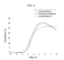
- FIG. 6 is a graph showing transmittance according to a driving voltage of the transflective liquid crystal display of FIG. 1 in comparison with a liquid crystal display according to a prior art.
- FIG. 7 is a graph showing reflectivity according to a driving voltage of the transflective liquid crystal display of FIG. 1 in comparison with the liquid crystal display according to the prior art.
- FIG. 8 is a cross-sectional view of another exemplary embodiment of a transflective liquid crystal display according to the invention.
- FIG. 9 and FIG. 10 show a driving mechanism of a reflection mode of the transflective liquid crystal display of FIG. 8 .
- FIG. 11 and FIG. 12 show a driving mechanism of a transmission mode of the transflective liquid crystal display of FIG. 8 .
- FIG. 13 is a cross-sectional view of another exemplary embodiment of a transflective liquid crystal display according to the invention.
- FIG. 14 and FIG. 15 show a driving mechanism of a reflection mode of the transflective liquid crystal display of FIG. 13 .
- FIG. 16 and FIG. 17 show a driving mechanism of a transmission mode of the transflective liquid crystal display of FIG. 13 .
- FIG. 18 is a cross-sectional view of another exemplary embodiment of a transflective liquid crystal display according to the invention.
- FIG. 19 and FIG. 20 show a driving mechanism of a reflection mode of the transflective liquid crystal display of FIG. 18 .
- FIG. 21 and FIG. 22 show a driving mechanism of a transmission mode of the transflective liquid crystal display of FIG. 18 .
- FIG. 23 is a cross-sectional view of another exemplary embodiment of a transflective liquid crystal display according to the invention.
- FIG. 24 and FIG. 25 show a driving mechanism of a reflection mode of the transflective liquid crystal display of FIG. 23 .
- FIG. 26 and FIG. 27 show a driving mechanism of a transmission mode of the transflective liquid crystal display of FIG. 23 .
- first, second, third, etc. may be used herein to describe various elements, components, regions, layers and/or sections, these elements, components, regions, layers and/or sections should not be limited by these terms. These terms are only used to distinguish one element, component, region, layer or section from another region, layer or section. Thus, a first element, component, region, layer or section discussed below could be termed a second element, component, region, layer or section without departing from the teachings of the invention.
- spatially relative terms such as “lower,” “upper” and the like, may be used herein for ease of description to describe the relationship of one element or feature to another element(s) or feature(s) as illustrated in the figures. It will be understood that the spatially relative terms are intended to encompass different orientations of the device in use or operation, in addition to the orientation depicted in the figures. For example, if the device in the figures is turned over, elements described as “lower” relative to other elements or features would then be oriented “upper” relative to the other elements or features. Thus, the exemplary term “below” can encompass both an orientation of above and below. The device may be otherwise oriented (rotated 90 degrees or at other orientations) and the spatially relative descriptors used herein interpreted accordingly.
- FIG. 1 is a cross-sectional view of an exemplary embodiment of a transflective liquid crystal display according to the invention.
- the transflective liquid crystal display includes a liquid crystal panel including a lower panel including a first substrate 110 , an upper panel including a second substrate 210 , and a liquid crystal layer 3 between the lower and upper panels.
- the first and second substrates 110 and 210 are arranged to face each other.
- first gate lines, first data lines, and a first thin film transistor connected to the first gate lines and the first data lines are on the first substrate 110 .
- the first gate lines and the first data lines cross each other and define a plurality of pixels, but the invention is not limited thereto.
- the first thin film transistor includes a first gate electrode 124 on the first substrate 110 , a first gate insulating layer 140 on the first gate electrode 124 , a first semiconductor layer 151 on the first gate insulating layer 140 , a first source electrode 173 , and a first drain electrode 175 .
- the first source electrode 173 and the first drain electrode 175 are at a distance from each other on the first semiconductor 151 , and form a channel therebetween.
- a first passivation layer 180 is on the first source electrode 173 and the first drain electrode 175 , and a first pixel electrode 191 is in a pixel and on the first passivation layer 180 .
- a common electrode 132 is in a pixel under the first pixel electrode 191 .
- the first pixel electrode 191 is in the shape of a plurality of bars connected to each other, and a horizontal electric field may be formed between the first pixel electrode 191 and the common electrode 132 .
- a bar indicates an elongated shape, having a length substantially greater than a width.
- second gate lines, second data lines, and a second thin film transistor connected to the second gate lines and the second data lines are on the second substrate 210 .
- the second gate lines and the second data lines cross each other, defining a plurality of pixels, but the invention is not limited thereto.
- the second thin film transistor includes a second gate electrode 224 on the second substrate 210 , a second gate insulating layer 240 on the second gate electrode 224 , a second semiconductor layer 251 on the second gate insulating layer 240 , a second source electrode 273 , and a second drain electrode 275 .
- the second source electrode 273 and the second drain electrode 275 are at a distance from each other on the second semiconductor layer 251 , and form a channel therebetween.
- a second passivation layer 280 is on the second source electrode 273 and the second drain electrode 275 , and a second pixel electrode 291 is in a pixel and on the second passivation layer 280 .
- a vertical electric field may be formed between the second pixel electrode 291 and the common electrode 132 .
- the liquid crystal layer 3 includes a mixture of a plurality of liquid crystal molecules 31 and a dichroic dye 33 .
- the liquid crystal layer 3 is arranged in a direction parallel with the first substrate 110 and the second substrate 210 .
- a reflection polarizer 12 and an absorption polarizer 22 are on outer sides of the liquid crystal panel.
- the reflection polarizer 12 may be attached to an outer side of the lower panel including the first substrate 110
- the absorption polarizer 22 may be attached to an outer side of the upper panel including the second substrate 210 .
- a backlight unit 50 is at the outer side of the liquid crystal panel, that is, the outer side of the lower panel including the first substrate 110 .
- the backlight unit 50 is classified as a direct backlight type or a side backlight type according to alignment of a light source.
- the direct type is one in which a lamp disposed under and overlapping the liquid crystal panel directly irradiates light to the liquid crystal panel
- the side type is one in which light is irradiated to the liquid crystal panel through a light guiding plate.
- the backlight unit 50 according to the invention may adopt either of the two types.
- the backlight unit 50 supplies light to the inner side of the liquid crystal panel, and the supplied light is transmitted to the outer side of the liquid crystal panel, that is, the outer side of the upper panel including the second substrate 210 , such that an image is displayed on a screen of the liquid crystal panel.
- FIG. 2 and FIG. 3 show a driving mechanism of the reflection mode of the transflective liquid crystal display of FIG. 1
- FIG. 4 and FIG. 5 show a driving mechanism of the transmission mode of the transflective liquid crystal display of FIG. 1 .
- the reflection polarizer 12 of the transflective liquid crystal display of FIG. 1 has a reflective axis RA reflecting light that vibrates in a first direction, and a transmissive axis TA 1 transmitting light that vibrates in a second direction that is substantially perpendicular to the first direction.
- the absorption polarizer 22 has a transmissive axis TA 2 that transmits light vibrating in the first direction.
- the reflective axis RA of the reflection polarizer 12 is parallel with the transmissive axis TA 2 of the absorption polarizer 22
- the transmissive axis TA 1 of the reflection polarizer 12 is perpendicular to the transmissive axis TA 2 of the absorption polarizer 22 .
- the liquid crystal layer 3 is arranged in a direction that is parallel with the reflective axis RA of the reflection polarizer 12 . Thus, when the light vibrating in the first direction enters into the liquid crystal layer 3 , the light is absorbed by the dichroic dye 33 .
- the liquid crystal layer 3 is arranged in a direction that is perpendicular to the reflection polarizer 12 and the absorption polarizer 22 .
- the light having passed through the absorption polarizer 22 can reach the reflection polarizer 12 without being absorbed by the dichroic dye 33 .
- the light reaching the reflection polarizer 12 vibrates in the first direction that is parallel with the reflective axis RA of the reflection polarizer 12 , the light is reflected by the reflection polarizer 12 and thus reaches the absorption polarizer 22 . Since the light reaching the absorption polarizer 22 vibrates in the first direction that is parallel with the transmissive axis TA 2 of the absorption polarizer 22 , the light is transmitted to the outside of the liquid crystal panel through the absorption polarizer 22 . Accordingly, when the vertical electric field is formed in the reflection mode, a white gray can be expressed.
- the transmission mode when light vibrating in the first and second directions enters from the backlight unit 50 , only the light vibrating in the second direction parallel with the transmissive axis TA 1 of the reflection polarizer 12 is passed through the reflection polarizer 12 , and the light vibrating in the first direction is reflected by the reflection polarizer 12 .
- the light having passed through the reflection polarizer 12 can reach the absorption polarizer 22 without being absorbed by the dichroic dye 33 .
- the black gray can be expressed.
- the reflection mode When the white gray of the transmission mode is expressed, the reflection mode also expresses a white mode so that gray inversion can be reduced or effectively prevented.
- the reflection mode when a black gray is expressed in the transmission mode, the reflection mode also expresses a black gray, and when a white gray is expressed in the transmission mode, the reflection mode also expresses a white gray. That is, when the transmission mode expresses a black gray, the black gray can be further clearly expressed by reducing or effectively preventing reflection of the light, and when the transmission mode expresses a white gray, the white gray can be further clearly expressed by controlling light entering from the outside to be reflected.
- the reason for this is that when the dichroic dye 33 is arranged in a direction perpendicular to the reflective axis RA of the reflection polarizer 12 , light entering from the outside can reach the reflection polarizer 12 without being absorbed by the dichroic dye 33 , but when the dichroic dye 33 is arranged in a direction parallel with the reflective axis RA of the reflection polarizer 12 , the light cannot reach the reflection polarizer 12 and thus cannot be reflected to the outside because it is absorbed by the dichroic dye 33 .
- FIG. 6 is a graph showing transmittance according to a driving voltage of the transflective liquid crystal display of FIG. 1 in comparison with a liquid crystal display according to a conventional art
- FIG. 7 is a graph showing reflectivity according to the driving voltage of the transflective liquid crystal display of FIG. 1 in comparison with the liquid crystal display according to the conventional art.
- Conventional art 1 indicates a general backlit liquid crystal display, and transmittance is measured using a fringe field switching mode liquid crystal display
- Conventional art 2 indicates a transflective liquid crystal display formed of two conventional liquid crystal panels.
- a transmittance characteristic of the transflective liquid crystal display of the exemplary embodiment in FIG. 1 of the invention is similar to that of the general backlit liquid crystal display, and transmittance of the transflective liquid crystal display of the exemplary embodiment of FIG. 1 of the invention is higher than that of the transflective liquid crystal display formed of the two conventional liquid crystal panels.
- the transflective liquid crystal display of the invention has higher reflectivity than a conventional transflective liquid crystal formed of two liquid crystal panels.
- a difference between reflectivity in the black gray and reflectivity in the white gray is increased so that the contrast ratio is also increased.
- FIG. 8 is a cross-sectional view of another exemplary embodiment of a transflective liquid crystal display according to the invention.
- the transflective liquid crystal display of FIG. 8 is similar to the transflective liquid crystal display of FIG. 1 , and therefore different parts from the exemplary embodiment of FIG. 1 will be described.
- the transflective liquid crystal display of FIG. 8 includes the liquid crystal panel including the lower panel including the first substrate 110 , the upper panel including the second substrate 210 , and the liquid crystal layer 3 between the lower and upper panels.
- the first and second substrates 110 and 210 are arranged to face each other.
- liquid crystal layer 3 of FIG. 1 is arranged in the horizontal direction, but the liquid crystal layer 3 of FIG. 8 is arranged in a direction that is perpendicular to the first and second substrates 110 and 210 .
- the reflection polarizer 12 , the absorption polarizer 22 , and the backlight unit 50 are the same as those in the first exemplary embodiment.
- FIG. 9 and FIG. 10 show a driving mechanism of the reflection mode of the transflective liquid crystal display of FIG. 8
- FIG. 11 and FIG. 12 show a driving mechanism of the transmission mode of the transflective liquid crystal display of FIG. 8 .
- the reflection polarizer 12 of the transflective liquid crystal display of FIG. 8 has a transmissive axis TA 1 transmitting light that vibrates in a first direction and a reflective axis RA reflecting light that vibrates in a second direction that is substantially perpendicular to the first direction.
- the absorption polarizer 22 further has a transmissive axis TA 2 that transmits light vibrating in the second direction.
- the reflective axis RA of the reflection polarizer 12 is parallel with the transmissive axis TA 2 of the absorption polarizer 22
- the transmissive axis TA 1 of the reflection polarizer 12 is perpendicular to the transmissive axis TA 2 of the absorption polarizer 22 .
- Alignment of the liquid crystal layer 3 of the transflective liquid crystal display of FIG. 8 is different from that of the liquid crystal layer 3 of the transflective liquid crystal display of FIG. 1 , and is arranged in a direction that is perpendicular to the reflection polarizer 12 and the absorption polarizer 22 .
- the light is not absorbed by the dichroic dye 33 .
- the liquid crystal layer 3 is arranged in a direction that is perpendicular to the absorption polarizer 22 , and the light having passed through the absorption polarizer 22 passes through the liquid crystal layer 3 without phase variation so that the light can reach the reflection polarizer 12 without being absorbed by the dichroic dye 33 .
- the reflection polarizer 12 Since the light having reached the reflection polarizer 12 vibrates in the second direction that is parallel with the reflective axis RA of the reflection polarizer 12 , that light is reflected by the reflection polarizer 12 and then reaches the absorption polarizer 22 . Since the light having reached the absorption polarizer 22 vibrates in the second direction that is parallel with the transmissive axis TA 2 of the absorption polarizer 22 , the light is transmitted through the absorption polarizer 22 to the outside of the liquid crystal panel. Therefore, when no electric field is formed in the reflection mode, a white gray can be expressed.
- the liquid crystal layer 3 is arranged in a direction that is parallel with the reflective axis RA of the reflection polarizer 12 .
- the light having passed through the absorption polarizer 22 passes into the liquid crystal layer 3 without phase variation and vibrates in the second direction, the light is absorbed by the dichroic dye 33 when entering into the liquid crystal layer 3 . Therefore, when the vertical electric field is formed in the reflection mode, a black gray can be expressed.
- the liquid crystal layer 3 rotates and the phase of the light having passed through the liquid crystal layer 3 is changed 90 degrees to be parallel with the reflective axis RA of the reflection polarizer 12 . Therefore, the light having passed through the liquid crystal layer 3 can reach the absorption polarizer 22 without being absorbed by the dichroic dye 33 . Since the light reaching the absorption polarizer 22 vibrates in the second direction that is parallel with the transmissive axis TA 2 of the absorption polarizer 22 , the light is transmitted through the absorption polarizer 22 to the outside of the liquid crystal panel. Therefore, when the horizontal electric field and the vertical electric field are formed in the transmission mode, a white gray can be expressed.
- the liquid crystal layer 3 is arranged in a direction that is perpendicular parallel with the reflective axis RA of the reflection polarizer 12 .
- the light having passed through the reflection polarizer 12 can reach the absorption polarizer 22 without being absorbed by the dichroic dye 33 , and the light vibrates in the first direction that is perpendicular to the transmissive axis TA 2 of the absorption polarizer 22 , and therefore the light is absorbed by the absorption polarizer 22 . Therefore, when the vertical electric field is formed in the transmission mode, a black gray can be expressed.
- the reflection mode also expresses the black gray so that gray inversion can be reduced or effectively prevented.
- FIG. 13 is a cross-sectional view of another exemplary embodiment of a transflective liquid crystal display according to the invention.
- the transflective liquid crystal display of FIG. 13 is similar to the transflective liquid crystal display of FIG. 1 , and therefore different parts from the exemplary embodiment of FIG. 1 will be described.
- the transflective liquid crystal display of FIG. 13 includes the liquid crystal panel including the lower panel including the first substrate 110 , the upper panel including the second substrate 210 , and the liquid crystal layer 3 between the lower and upper panels.
- the first and second substrates 110 and 210 are arranged to face each other.
- the liquid crystal layer 3 of FIG. 1 is arranged in the horizontal direction, but the liquid crystal layer 3 of FIG. 13 is arranged in parallel with the first substrate 110 in a portion adjacent to the first substrate 110 , and arranged in a direction perpendicular to the second substrate 210 in a portion adjacent to the second substrate 210 .
- the reflection polarizer 12 , the absorption polarizer 22 , and the backlight unit 50 are the same as those in the first exemplary embodiment.
- FIG. 14 and FIG. 15 show a driving mechanism of the reflection mode of the transflective liquid crystal display of FIG. 13
- FIG. 16 and FIG. 17 show a driving mechanism of the transmission mode of the transflective liquid crystal display of FIG. 13 .
- the reflection polarizer 12 of the transflective liquid crystal display of FIG. 13 has a reflective axis RA reflecting light that vibrates in a first direction, and a transmissive axis TA 1 transmitting light that vibrates in a second direction that is substantially perpendicular to the first direction.
- the absorption polarizer 22 further has a transmissive axis TA 2 that transmits light vibrating in the first direction.
- the reflective axis RA of the reflection polarizer 12 is parallel with the transmissive axis TA 2 of the absorption polarizer 22
- the transmissive axis TA 1 of the reflection polarizer 12 is perpendicular to the transmissive axis TA 2 of the absorption polarizer 22 .
- the liquid crystal layer 3 is arranged in parallel with the reflective axis RA of the reflection polarizer 12 in a portion adjacent to the first substrate 110 of FIG. 13 . Therefore, when the light vibrating in the first direction enters into the liquid crystal layer 3 , the light is absorbed by the dichroic dye 33 .
- the liquid crystal layer 3 is arranged in a direction that is perpendicular to the reflection polarizer 12 in a portion adjacent to the second substrate 210 of FIG. 13 .
- the reflection mode when light vibrating in the first and second directions enters from the outside, only the light vibrating in the first direction that is parallel with the transmissive axis TA 2 of the absorption polarizer 22 passes through the absorption polarizer 22 , and the light vibrating in the second direction is absorbed by the absorption polarizer 22 .
- the light having passed through the absorption polarizer 22 passes through the liquid crystal layer 3 without phase variation, and vibrates in the first direction, and thus when the light enters into the liquid crystal layer 3 , the light is absorbed by the dichroic dye 33 . Therefore, when no electric field is formed in the reflection mode, a black gray can be expressed.
- the liquid crystal layer 3 is arranged in a direction that is perpendicular to the reflection polarizer 12 and the absorption polarizer 22 .
- the light having passed through the absorption polarizer 22 can reach the reflection polarizer 12 without being absorbed by the dichroic dye 33 . Since the light reaching the reflection polarizer 12 vibrates in the first direction that is parallel with the reflective axis RA of the reflection polarizer 12 , the light is reflected by the reflection polarizer 12 and thus reaches the absorption polarizer 22 . The light having reached the absorption polarizer 22 vibrates in the first direction that is parallel with the transmissive axis TA 2 of the absorption polarizer 22 so that the light is transmitted through the absorption polarizer 22 to the outside of the liquid crystal panel. Therefore, when the vertical electric field is formed in the reflection mode, a white gray can be expressed.
- the transmission mode when light vibrating in the first and second directions enters from the backlight unit 50 , only light vibrating in the second direction that is parallel with the transmissive axis TA 1 of the reflection polarizer 12 passes through the reflection polarizer 12 , and light vibrating in the first direction is reflected by the reflection polarizer 12 .
- the light having passed through the reflection polarizer 12 can reach the absorption polarizer 22 without being absorbed by the dichroic dye 33 .
- the gray of the reflection mode can also be expressed.
- the black gray is expressed in the reflection mode when expressing the black gray in the transmission mode so that gray inversion can be reduced or effectively prevented.
- the light having reached the absorption polarizer 22 vibrates in the first direction that is parallel with the transmissive axis TA 2 of the absorption polarizer 22 , and therefore the light is expressed to the outside of the liquid crystal panel. Accordingly, when the horizontal electric field is formed in the transmission mode, a white gray can be expressed.
- the white gray When expressing the white gray in the transmission mode, the white gray is also expressed in the reflection mode so that gray inversion can be reduced or effectively prevented.
- FIG. 18 is a cross-sectional view of a transflective liquid crystal display according to the invention.
- the transflective liquid crystal display of FIG. 18 includes the liquid crystal panel including the lower panel including the first substrate 110 , the upper panel including the second substrate 210 , and the liquid crystal layer 3 between the lower and upper panels.
- the first and second substrates 110 and 210 are arranged to face each other.
- the transflective liquid crystal display further includes an auxiliary liquid crystal panel including a third substrate 310 , a fourth substrate 410 , and an auxiliary liquid crystal layer 6 between the third and fourth substrates 310 and 410 .
- first gate lines, first data lines, and a first thin film transistor are on the first substrate 110 .
- the first gate lines and the first data lines cross each other and define a plurality of pixels, but the invention is not limited thereto.
- the first thin film transistor includes the first gate electrode 124 on the first substrate 110 , the first gate insulating layer 140 on the first gate electrode 124 , the first semiconductor layer 151 on the first gate insulating layer 140 , the first source electrode 173 , and the first drain electrode 175 .
- the first source electrode 173 and the first drain electrode 175 are at a distance from each other on the first semiconductor layer 151 .
- the first passivation layer 180 is on the first source electrode 173 and the first drain electrode 175
- the first pixel electrode 191 is in a pixel and on the first passivation layer 180 .
- a first common electrode 270 is on the second substrate 210 . Since the first substrate 110 and the second substrate 210 are arranged to face each other, a vertical electric field may be formed between the first pixel electrode 191 and the first common electrode 270 when a voltage is applied to the first pixel electrode 191 and the first common electrode 270 .
- the liquid crystal layer 3 includes a mixture of a plurality of the liquid crystal molecules 31 and the dichroic dye 33 .
- the liquid crystal layer 3 is arranged in a direction perpendicular to the first substrate 110 and the second substrate 210 .
- second gate lines, second data lines, and a second thin film transistor connected to the second gate line and the second data line are on the third substrate 310 of the auxiliary liquid crystal panel.
- the second gate lines and the second data lines cross each other and define a plurality of pixels, but the invention is not limited thereto.
- the second thin film transistor includes the second gate electrode 224 on the third substrate 310 , the second gate insulating layer 240 on the second gate electrode 224 , the second semiconductor layer 251 on the second gate insulating layer 240 , the second source electrode 273 , and the second drain electrode 275 .
- the second source electrode 273 and the second drain electrode 275 are at a distance from each other on the second semiconductor layer 251 .
- the second passivation layer 280 is on the second source electrode 273 and the second drain electrode 275
- the second pixel electrode 291 is in a pixel and on the second passivation layer 280 .
- a second common electrode 470 is on the fourth substrate 410 of the auxiliary liquid crystal panel. Since the third substrate 310 is arranged to face the fourth substrate 410 , a vertical electric field may be formed between the second pixel electrode 291 and the second common electrode 470 when a voltage is applied to the second pixel electrode 291 and the second common electrode 470 .
- the auxiliary liquid crystal layer 6 is arranged in a direction that is parallel with the third substrate 310 and the fourth substrate 410 .
- the reflection polarizer 12 and the absorption polarizer 22 are formed on outer sides of the liquid crystal panel and the auxiliary liquid crystal panel.
- the reflection polarizer 12 may be attached between the liquid crystal panel and the auxiliary liquid crystal panel, that is, directly between the first substrate 110 and the fourth substrate 410 .
- the absorption polarizer 22 may be attached to an outer side of the auxiliary liquid crystal panel, that is, directly on an outer side of the third substrate 310 .
- the backlight unit 50 is at the outer side of the auxiliary liquid crystal panel, that is, the outer side of the third substrate 310 .
- the absorption polarizer 22 is disposed between the third substrate 310 of the auxiliary liquid crystal panel and the backlight unit 50 .
- the backlight unit 50 supplies light to the inside of the auxiliary liquid crystal panel, and the supplied light emits to the outer side of the auxiliary liquid crystal panel, more particularly, to an outer side of the fourth substrate 410 , and then enters to the inner side of the liquid crystal panel, more particularly, to an inner side of the first substrate 110 .
- the light supplied to the inner side of the liquid crystal panel is emitted to the outer side of the liquid crystal panel. More particularly, the light is emitted to the outer side of the second substrate 210 and expressed in the screen of the transflective liquid crystal display.
- FIG. 19 and FIG. 20 show a driving mechanism of the reflection mode of the transflective liquid crystal display of FIG. 18
- FIG. 21 and FIG. 22 show a driving mechanism of the transmission mode of the transflective liquid crystal display of FIG. 18 .
- the reflection polarizer 12 of the transflective liquid crystal display of FIG. 18 has a reflective axis RA reflecting light that vibrates in a first direction, and a transmissive axis TA 1 transmitting light that vibrates in a second direction that is substantially perpendicular to the first direction.
- the absorption polarizer 22 further has a transmissive axis TA 2 that transmits light vibrating in the first direction.
- the reflective axis RA of the reflection polarizer 12 is parallel with the transmissive axis TA 2 of the absorption polarizer 22
- the transmissive axis TA 1 of the reflection polarizer 12 is perpendicular to the transmissive axis TA 2 of the absorption polarizer 22 .
- the liquid crystal panel 3 is arranged in a direction that is perpendicular to the reflection polarizer 12 , and the auxiliary liquid crystal layer 6 of the auxiliary liquid crystal panel is arranged in a direction that is parallel with the reflection polarizer 12 .
- the reflection polarizer 12 Among the light reaching the reflection polarizer 12 , light vibrating in the second direction that is parallel with the transmissive axis TA 1 of the reflection polarizer 12 passes through the reflection polarizer 12 and then reaches the absorption polarizer 22 , and the light vibrates in the direction that is perpendicular to the transmissive axis TA 2 of the absorption polarizer 22 and therefore it is absorbed by the absorption polarizer 22 .
- light vibrating in the first direction that is parallel with the reflective axis RA of the reflection polarizer 12 is reflected by the reflection polarizer 12 and thus expressed to the outside of the liquid crystal panel. Accordingly, when no electric field is formed in the liquid crystal panel and the auxiliary liquid crystal panel, a white gray can be expressed.
- the liquid crystal layer 3 is arranged in a direction that is parallel with the reflective axis RA of the reflection polarizer 12 so that light vibrating in the first direction that is parallel with the dichroic dye 33 is absorbed by the dichroic dye 33 , and light vibrating in the second direction that is parallel with the transmissive axis TA 1 of the reflection polarizer 12 passes through the reflection polarizer 12 .
- the light having passed through the reflection polarizer 12 reaches the absorption polarizer 22 without phase variation in the state in which no electric field is formed, and the light vibrates in a direction that is perpendicular to the transmissive axis TA 2 of the absorption polarizer 22 and therefore it is absorbed by the absorption polarizer 22 . Accordingly, when a vertical electric field is formed in the liquid crystal panel in the reflection mode, a black gray can be expressed.
- the reflection polarizer 12 Since the light reaching the reflection polarizer 12 is vibrating in the first direction that is parallel with the reflective axis RA of the reflection polarizer 12 , the light is reflected by the reflection polarizer 12 and thus the light cannot enter into the liquid crystal panel. Accordingly, in the transmission mode, when no electric field is formed in the auxiliary liquid crystal panel, a black gray can be expressed.
- a voltage is applied to the first pixel electrode 191 of FIG. 18 and the first common electrode 270 of FIG. 18 in the liquid crystal panel and thus a vertical electric field is formed, and the liquid crystal layer 3 is arranged in a direction that is parallel with the reflective axis RA of the reflection polarizer 12 . Therefore, light entering from the outside cannot be emitted to the outside in the reflection mode so that a black gray can be expressed. That is, when expressing the black gray in the transmission mode, the black gray is also expressed in the reflection mode when the vertical electric field is formed in the liquid crystal panel so that gray inversion can be reduced or effectively prevented.
- the auxiliary liquid crystal layer 6 rotates and the light having passed through the auxiliary liquid crystal layer 6 is changed 90 degrees.
- the light having passed through the auxiliary liquid crystal layer 6 vibrates in the second direction that is parallel with the transmissive axis TA 1 of the reflection polarizer 12 , and therefore the light can pass through the reflection polarizer 12 .
- the light having passed through the reflection polarizer 12 passes through the liquid crystal layer 3 without phase variation, and the liquid crystal layer 3 is arranged in a direction that is perpendicular to the reflection polarizer 12 so that the light vibrating in the second direction is expressed to the outside of the liquid crystal panel without being absorbed by the dichroic dye 33 . Accordingly, when an electric field is not formed in the liquid crystal panel and a vertical electric field is formed in the auxiliary liquid crystal panel in the transmission mode, a white gray can be expressed.
- the white gray When a white gray is expressed in the transmission mode, the white gray is also expressed in the reflection mode so that gray inversion can be reduced or effectively prevented.
- FIG. 23 is a cross-sectional view of another exemplary embodiment of a transflective liquid crystal display according to the invention.
- the transflective liquid crystal display of FIG. 23 is similar to the transflective liquid crystal display of FIG. 18 , and therefore different parts from the exemplary embodiment in FIG. 18 will be described.
- the transflective liquid crystal display of FIG. 23 includes the liquid crystal panel including the first substrate 110 , the second substrate 210 , and the liquid crystal layer 3 between the first and second substrates 110 and 210 , and the auxiliary crystal display panel including the third substrate 310 , the fourth substrate 410 , and the auxiliary liquid crystal layer 6 between the third and fourth substrates 310 and 410 .
- the first and second substrates 110 and 210 are arranged to face each other, and the third and fourth substrates 310 and 410 are arranged to face each other.
- liquid crystal layer 3 is arranged in the vertical direction in FIG. 18 , but the liquid crystal layer 3 in FIG. 23 is arranged in a direction that is parallel with the first and second substrates 110 and 210 .
- the auxiliary liquid crystal layer 6 , the reflection polarizer 12 , the absorption polarizer 22 , and the backlight unit 50 are the same as those of FIG. 18 .
- FIG. 24 and FIG. 25 show a driving mechanism of the reflection mode of the transflective liquid crystal display of FIG. 23
- FIG. 26 and FIG. 27 show a driving mechanism of the transmission mode of the transflective liquid crystal display of FIG. 23 .
- the reflection polarizer 12 of the transflective liquid crystal display of FIG. 23 has a reflective axis RA reflecting light that vibrates in a first direction, and a transmissive axis TA 1 transmitting light that vibrates in a second direction that is substantially perpendicular to the first direction.
- the absorption polarizer 22 further has a transmissive axis TA 2 that transmits light vibrating in the first direction.
- the reflective axis RA of the reflection polarizer 12 is parallel with the transmissive axis TA 2 of the absorption polarizer 22
- the transmissive axis TA 1 of the reflection polarizer 12 is perpendicular to the transmissive axis TA 2 of the absorption polarizer 22 .
- the liquid crystal panel 3 is arranged in a direction that is parallel with to the reflection polarizer 12 , and the auxiliary liquid crystal layer 6 of the auxiliary liquid crystal panel is arranged in a direction that is parallel with the reflection polarizer 12 .
- the light having passed through the reflection polarizer 12 reaches the absorption polarizer 22 without phase variation, and the light vibrates in a direction that is perpendicular to the transmissive axis TA 2 of the absorption polarizer 22 so that the light is absorbed by the absorption polarizer 22 . Accordingly, a black gray can be expressed in the reflection mode when no electric field is formed in the liquid crystal panel and the auxiliary liquid crystal panel.
- the liquid crystal layer 3 is arranged in a direction perpendicular to the reflection polarizer 12 so that the light vibrating in the first and second directions can reach the reflection polarizer 12 without being absorbed by the dichroic dye 33 .
- the reflection polarizer 12 Among the light reaching the reflection polarizer 12 , light vibrating in the second direction that is parallel with a transmissive axis TA 1 of the reflection polarizer 12 passes through the reflection polarizer 12 in the state in which no electric field is formed in the auxiliary liquid crystal panel and then reaches the absorption polarizer 22 . Since the light reaching the absorption polarizer 22 vibrates in the second direction that is perpendicular to a transmissive axis TA 2 of the absorption polarizer 22 , the light is absorbed by the absorption polarizer 22 .
- the reflection polarizer 12 Among the light reaching the reflection polarizer 12 , light vibrating in the first direction that is parallel with a reflective axis RA of the reflection polarizer 12 is reflected by the reflection polarizer 12 and then expressed to the outside of the liquid crystal panel. Accordingly, when a vertical field is formed in the liquid crystal panel in the reflection mode, a white gray can be expressed.
- the reflection polarizer 12 Since the light reaching the reflection polarizer 12 vibrates in the first direction that is parallel with the reflective axis RA of the reflection polarizer 12 , the light is reflected by the reflection polarizer 12 so that the light cannot enter into the liquid crystal panel. Accordingly, when no electric field is formed in the auxiliary crystal display panel in the transmission mode, a black gray can be expressed.
- the black gray When expressing the black gray in the transmission mode, the black gray is also expressed in the reflection mode if no electric field is formed in the liquid crystal panel so that gray inversion can be reduced or effectively prevented.
- the liquid crystal layer 3 When a voltage is applied to a first pixel electrode 191 of FIG. 23 and a common electrode 270 of FIG. 23 in the liquid crystal panel and thus a vertical electric field is formed, the liquid crystal layer 3 is arranged in a direction that is perpendicular to the reflection polarizer 12 and thus light is expressed to the outside of the liquid crystal panel without being absorbed by the dichroic dye 33 . Accordingly, a white gray can be expressed in the transmission mode when a vertical electric field is formed in the liquid crystal panel and the auxiliary liquid crystal panel.
- the white gray When a white gray is expressed in the transmission mode, the white gray is also expressed in the reflection mode so that gray inversion can be reduced or effectively prevented.
- the transflective liquid crystal displays of FIGS. 18 to 22 and 23 to 27 are exemplary embodiments in which the transflective liquid crystal displays of FIGS. 1 to 5 , 8 to 12 and 13 to 17 can be realized using two liquid crystal panels.
Landscapes
- Physics & Mathematics (AREA)
- Nonlinear Science (AREA)
- General Physics & Mathematics (AREA)
- Optics & Photonics (AREA)
- Chemical & Material Sciences (AREA)
- Crystallography & Structural Chemistry (AREA)
- Mathematical Physics (AREA)
- Liquid Crystal (AREA)
- Engineering & Computer Science (AREA)
- Microelectronics & Electronic Packaging (AREA)
- Geometry (AREA)
Abstract
Description
Claims (22)
Applications Claiming Priority (2)
| Application Number | Priority Date | Filing Date | Title |
|---|---|---|---|
| KR1020110010214A KR101762370B1 (en) | 2011-02-01 | 2011-02-01 | Reflective and transparent type liquid crystal display device |
| KR10-2011-0010214 | 2011-02-01 |
Publications (2)
| Publication Number | Publication Date |
|---|---|
| US20120194763A1 US20120194763A1 (en) | 2012-08-02 |
| US8634043B2 true US8634043B2 (en) | 2014-01-21 |
Family
ID=46577099
Family Applications (1)
| Application Number | Title | Priority Date | Filing Date |
|---|---|---|---|
| US13/286,403 Expired - Fee Related US8634043B2 (en) | 2011-02-01 | 2011-11-01 | Reflective and transparent liquid crystal display device |
Country Status (2)
| Country | Link |
|---|---|
| US (1) | US8634043B2 (en) |
| KR (1) | KR101762370B1 (en) |
Families Citing this family (16)
| Publication number | Priority date | Publication date | Assignee | Title |
|---|---|---|---|---|
| GB2504936B (en) * | 2012-08-13 | 2014-09-10 | Electronic Temperature Instr Ltd | A display assembly |
| CN102830534A (en) * | 2012-08-23 | 2012-12-19 | 京东方科技集团股份有限公司 | Color film substrate, array substrate, liquid crystal display device and method for manufacturing color film substrate and array substrate |
| EP2878997A1 (en) * | 2013-11-27 | 2015-06-03 | The Swatch Group Research and Development Ltd. | Device for displaying information with dichroic liquid crystal |
| JP6255973B2 (en) * | 2013-12-18 | 2018-01-10 | セイコーエプソン株式会社 | Electro-optical device and electronic apparatus |
| JP6354406B2 (en) * | 2014-07-10 | 2018-07-11 | セイコーエプソン株式会社 | Electro-optical device and electronic apparatus |
| CN104216166A (en) * | 2014-09-15 | 2014-12-17 | 京东方科技集团股份有限公司 | Reflecting display panel, manufacture method thereof and display device |
| CN104570459B (en) * | 2014-12-31 | 2017-12-08 | 深圳市华星光电技术有限公司 | Liquid crystal panel |
| KR20170059054A (en) | 2015-11-19 | 2017-05-30 | 삼성디스플레이 주식회사 | Liquid crystal display |
| WO2017146545A1 (en) * | 2016-02-26 | 2017-08-31 | 주식회사 엘지화학 | Variable reflectivity mirror |
| WO2017146546A1 (en) * | 2016-02-26 | 2017-08-31 | 주식회사 엘지화학 | Mirror display |
| TWI609213B (en) * | 2016-12-14 | 2017-12-21 | 國立中山大學 | Adjustable heat insulation windows |
| TWI655487B (en) * | 2016-12-23 | 2019-04-01 | 南韓商Lg化學股份有限公司 | Reflectance-variable mirror |
| JP6599029B2 (en) | 2017-01-27 | 2019-10-30 | 富士フイルム株式会社 | Liquid crystal display device, electronic device, display control method, display control program, and non-temporary recording medium |
| US10288968B2 (en) * | 2017-09-11 | 2019-05-14 | Visteon Global Technologies, Inc. | Electronic display with multiple polarizer layers |
| CN110543052A (en) * | 2019-08-28 | 2019-12-06 | 青岛海信电器股份有限公司 | Display device |
| CN115047673B (en) * | 2022-03-30 | 2024-03-12 | 昆山龙腾光电股份有限公司 | Liquid crystal display device having a light shielding layer |
Citations (17)
| Publication number | Priority date | Publication date | Assignee | Title |
|---|---|---|---|---|
| US5686979A (en) | 1995-06-26 | 1997-11-11 | Minnesota Mining And Manufacturing Company | Optical panel capable of switching between reflective and transmissive states |
| US6025897A (en) * | 1993-12-21 | 2000-02-15 | 3M Innovative Properties Co. | Display with reflective polarizer and randomizing cavity |
| JP2004069835A (en) | 2002-08-02 | 2004-03-04 | Sharp Corp | Liquid crystal display device |
| JP2004117750A (en) | 2002-09-25 | 2004-04-15 | Sharp Corp | Liquid crystal display |
| US20040095541A1 (en) * | 1999-05-13 | 2004-05-20 | International Business Machines Corporation | Liquid crystal display device and method for fabricating the same |
| JP2004163583A (en) | 2002-11-12 | 2004-06-10 | Seiko Epson Corp | Electrooptical device and electronic equipment |
| KR20060035331A (en) | 2004-10-22 | 2006-04-26 | 삼성전자주식회사 | Display apparatus |
| KR20060078052A (en) | 2004-12-30 | 2006-07-05 | 엘지.필립스 엘시디 주식회사 | Liquid crystal display device |
| KR20060134316A (en) | 2005-06-22 | 2006-12-28 | 삼성전자주식회사 | Liquid crystal display |
| JP2007219172A (en) | 2006-02-16 | 2007-08-30 | Sharp Corp | Liquid crystal display device |
| US20070263150A1 (en) * | 2006-04-05 | 2007-11-15 | Sony Corporation | Optical element, optical apparatus and imaging apparatus |
| JP2008185810A (en) | 2007-01-30 | 2008-08-14 | Asahi Kasei Corp | Liquid crystal display device |
| KR20080108770A (en) | 2007-06-11 | 2008-12-16 | 삼성전자주식회사 | Liquid crystal display device switchable between reflective mode and transmissive mode employing an active reflective polarizer |
| KR20100000322A (en) | 2008-06-24 | 2010-01-06 | 삼성전자주식회사 | Display apparatus switchable between transmissive mode and reflective mode |
| US20100177030A1 (en) * | 2007-06-04 | 2010-07-15 | Sharp Kabushiki Kaisha | Backlight unit, display unit and television receiver |
| US8289475B2 (en) * | 2008-10-28 | 2012-10-16 | Casio Computer Co., Ltd | Liquid crystal display apparatus |
| US8390750B2 (en) * | 2008-09-04 | 2013-03-05 | Hitachi Displays, Ltd. | Liquid crystal display device |
Family Cites Families (1)
| Publication number | Priority date | Publication date | Assignee | Title |
|---|---|---|---|---|
| JP2004341109A (en) * | 2003-05-14 | 2004-12-02 | Seiko Epson Corp | Liquid crystal display device and electronic equipment |
-
2011
- 2011-02-01 KR KR1020110010214A patent/KR101762370B1/en active IP Right Grant
- 2011-11-01 US US13/286,403 patent/US8634043B2/en not_active Expired - Fee Related
Patent Citations (17)
| Publication number | Priority date | Publication date | Assignee | Title |
|---|---|---|---|---|
| US6025897A (en) * | 1993-12-21 | 2000-02-15 | 3M Innovative Properties Co. | Display with reflective polarizer and randomizing cavity |
| US5686979A (en) | 1995-06-26 | 1997-11-11 | Minnesota Mining And Manufacturing Company | Optical panel capable of switching between reflective and transmissive states |
| US20040095541A1 (en) * | 1999-05-13 | 2004-05-20 | International Business Machines Corporation | Liquid crystal display device and method for fabricating the same |
| JP2004069835A (en) | 2002-08-02 | 2004-03-04 | Sharp Corp | Liquid crystal display device |
| JP2004117750A (en) | 2002-09-25 | 2004-04-15 | Sharp Corp | Liquid crystal display |
| JP2004163583A (en) | 2002-11-12 | 2004-06-10 | Seiko Epson Corp | Electrooptical device and electronic equipment |
| KR20060035331A (en) | 2004-10-22 | 2006-04-26 | 삼성전자주식회사 | Display apparatus |
| KR20060078052A (en) | 2004-12-30 | 2006-07-05 | 엘지.필립스 엘시디 주식회사 | Liquid crystal display device |
| KR20060134316A (en) | 2005-06-22 | 2006-12-28 | 삼성전자주식회사 | Liquid crystal display |
| JP2007219172A (en) | 2006-02-16 | 2007-08-30 | Sharp Corp | Liquid crystal display device |
| US20070263150A1 (en) * | 2006-04-05 | 2007-11-15 | Sony Corporation | Optical element, optical apparatus and imaging apparatus |
| JP2008185810A (en) | 2007-01-30 | 2008-08-14 | Asahi Kasei Corp | Liquid crystal display device |
| US20100177030A1 (en) * | 2007-06-04 | 2010-07-15 | Sharp Kabushiki Kaisha | Backlight unit, display unit and television receiver |
| KR20080108770A (en) | 2007-06-11 | 2008-12-16 | 삼성전자주식회사 | Liquid crystal display device switchable between reflective mode and transmissive mode employing an active reflective polarizer |
| KR20100000322A (en) | 2008-06-24 | 2010-01-06 | 삼성전자주식회사 | Display apparatus switchable between transmissive mode and reflective mode |
| US8390750B2 (en) * | 2008-09-04 | 2013-03-05 | Hitachi Displays, Ltd. | Liquid crystal display device |
| US8289475B2 (en) * | 2008-10-28 | 2012-10-16 | Casio Computer Co., Ltd | Liquid crystal display apparatus |
Non-Patent Citations (3)
| Title |
|---|
| "High Performance Reflective and Transflective Displays Using Guest-Host Liquid Crystal Gels" SID Tech. Digest 37, 780-782 (2006). |
| "Reflective and transflective color LCDs with double polarizers," Maeda et al., Journal of the Society for Information Display, Jul. 1, 1999. |
| "Transflective Liquid Crystal Display with High Aperture Ratio unsing Electrophoresis Particles," Cheong et al., IMID 2009 Digest. |
Also Published As
| Publication number | Publication date |
|---|---|
| US20120194763A1 (en) | 2012-08-02 |
| KR20120089082A (en) | 2012-08-09 |
| KR101762370B1 (en) | 2017-08-07 |
Similar Documents
| Publication | Publication Date | Title |
|---|---|---|
| US8634043B2 (en) | Reflective and transparent liquid crystal display device | |
| KR100518408B1 (en) | Dual liquid crystal display using of dual front light | |
| JP5623982B2 (en) | Transflective display device and electronic device | |
| US10663798B2 (en) | Liquid crystal display panel comprising a liquid crystal prism and a reflective prism disposed between first and second substrates and driving method thereof, and display device | |
| WO2009139199A1 (en) | Liquid crystal display device | |
| US9513505B2 (en) | Transflective liquid crystal display panel and liquid crystal display device | |
| JP5767195B2 (en) | Transflective display device, electronic apparatus, and driving method of transflective display device | |
| JP5239973B2 (en) | Liquid crystal display | |
| WO2009139198A1 (en) | Liquid crystal display device | |
| JP4760223B2 (en) | Liquid crystal device and electronic device | |
| US7889288B2 (en) | Dual reflective liquid crystal display device | |
| US20120147284A1 (en) | Liquid crystal display and the fabricating method of the same | |
| EP2508941B1 (en) | Transflective array substrate and transflective liquid-crystal display | |
| JP2008209858A (en) | Liquid crystal device and electronic equipment | |
| US7982833B2 (en) | Transflective liquid crystal display panel having a plurality of apertures with a specific ratio of aperture width to aperture interval | |
| JP2009075421A (en) | Liquid crystal device and electronic equipment | |
| US20050036082A1 (en) | Electro-optical crystal light shutter preventing motion picture blurring in a liquid crystal display | |
| WO2009113206A1 (en) | Liquid crystal display device | |
| KR100975750B1 (en) | Dual liquid crystal display using of dual front light | |
| JP2006301634A (en) | Display panel, method of manufacturing the same and display device having the same | |
| JP2008191480A (en) | Liquid crystal display device and electronic apparatus | |
| JP2005055645A (en) | Liquid crystal display element | |
| KR101633101B1 (en) | Trans-reflecting type liquid crystal display device | |
| KR101688593B1 (en) | In-plane switching mode transflective type liquid crystal display device | |
| JP2005258327A (en) | Liquid crystal display |
Legal Events
| Date | Code | Title | Description |
|---|---|---|---|
| AS | Assignment |
Owner name: PUSAN NATIONAL UNIVERISTY INDUSTRY-UNIVERSITY COOP Free format text: ASSIGNMENT OF ASSIGNORS INTEREST;ASSIGNORS:CHEONG, BYOUNG-HO;YOU, JAE-HO;RHO, SOON-JOON;AND OTHERS;SIGNING DATES FROM 20110523 TO 20110701;REEL/FRAME:027153/0443 Owner name: SAMSUNG ELECTRONICS CO., LTD., KOREA, REPUBLIC OF Free format text: ASSIGNMENT OF ASSIGNORS INTEREST;ASSIGNORS:CHEONG, BYOUNG-HO;YOU, JAE-HO;RHO, SOON-JOON;AND OTHERS;SIGNING DATES FROM 20110523 TO 20110701;REEL/FRAME:027153/0443 |
|
| AS | Assignment |
Owner name: SAMSUNG DISPLAY CO., LTD., KOREA, REPUBLIC OF Free format text: ASSIGNMENT OF ASSIGNORS INTEREST;ASSIGNOR:SAMSUNG ELECTRONICS CO., LTD.;REEL/FRAME:029151/0055 Effective date: 20120904 |
|
| AS | Assignment |
Owner name: PUSAN NATIONAL UNIVERSITY INDUSTRY-UNIVERSITY COOP Free format text: CORRECTIVE ASSIGNMENT TO CORRECT THE SPELLING OF THE SECOND ASSIGNEE'S NAME PREVIOUSLY RECORDED ON REEL 027153 FRAME 0443. ASSIGNOR(S) HEREBY CONFIRMS THE SECOND ASSIGNEE'S NAME IS "PUSAN NATIONAL UNIVERSITY INDUSTRY-UNIVERSITY COOPERATION FOUNDATION";ASSIGNORS:CHEONG, BYOUNG HO;YOU, JAE-HO;RHO, SOON-JOON;AND OTHERS;SIGNING DATES FROM 20110523 TO 20110701;REEL/FRAME:031768/0070 Owner name: SAMSUNG ELECTRONICS CO., LTD., KOREA, REPUBLIC OF Free format text: CORRECTIVE ASSIGNMENT TO CORRECT THE SPELLING OF THE SECOND ASSIGNEE'S NAME PREVIOUSLY RECORDED ON REEL 027153 FRAME 0443. ASSIGNOR(S) HEREBY CONFIRMS THE SECOND ASSIGNEE'S NAME IS "PUSAN NATIONAL UNIVERSITY INDUSTRY-UNIVERSITY COOPERATION FOUNDATION";ASSIGNORS:CHEONG, BYOUNG HO;YOU, JAE-HO;RHO, SOON-JOON;AND OTHERS;SIGNING DATES FROM 20110523 TO 20110701;REEL/FRAME:031768/0070 |
|
| STCF | Information on status: patent grant |
Free format text: PATENTED CASE |
|
| FEPP | Fee payment procedure |
Free format text: PAYOR NUMBER ASSIGNED (ORIGINAL EVENT CODE: ASPN); ENTITY STATUS OF PATENT OWNER: LARGE ENTITY |
|
| FPAY | Fee payment |
Year of fee payment: 4 |
|
| FEPP | Fee payment procedure |
Free format text: MAINTENANCE FEE REMINDER MAILED (ORIGINAL EVENT CODE: REM.); ENTITY STATUS OF PATENT OWNER: LARGE ENTITY |
|
| LAPS | Lapse for failure to pay maintenance fees |
Free format text: PATENT EXPIRED FOR FAILURE TO PAY MAINTENANCE FEES (ORIGINAL EVENT CODE: EXP.); ENTITY STATUS OF PATENT OWNER: LARGE ENTITY |
|
| STCH | Information on status: patent discontinuation |
Free format text: PATENT EXPIRED DUE TO NONPAYMENT OF MAINTENANCE FEES UNDER 37 CFR 1.362 |
|
| FP | Lapsed due to failure to pay maintenance fee |
Effective date: 20220121 |