US8633486B2 - Transistor structure and light emitting apparatus - Google Patents
Transistor structure and light emitting apparatus Download PDFInfo
- Publication number
- US8633486B2 US8633486B2 US13/179,015 US201113179015A US8633486B2 US 8633486 B2 US8633486 B2 US 8633486B2 US 201113179015 A US201113179015 A US 201113179015A US 8633486 B2 US8633486 B2 US 8633486B2
- Authority
- US
- United States
- Prior art keywords
- transistor
- film
- semiconductor film
- insulating film
- thin film
- Prior art date
- Legal status (The legal status is an assumption and is not a legal conclusion. Google has not performed a legal analysis and makes no representation as to the accuracy of the status listed.)
- Active, expires
Links
- 239000010408 film Substances 0.000 claims abstract description 1101
- 239000004065 semiconductor Substances 0.000 claims abstract description 574
- 239000010409 thin film Substances 0.000 claims abstract description 260
- XUIMIQQOPSSXEZ-UHFFFAOYSA-N Silicon Chemical compound [Si] XUIMIQQOPSSXEZ-UHFFFAOYSA-N 0.000 claims abstract description 139
- 229910052710 silicon Inorganic materials 0.000 claims abstract description 137
- 239000010703 silicon Substances 0.000 claims abstract description 137
- 238000002425 crystallisation Methods 0.000 claims abstract description 84
- 230000008025 crystallization Effects 0.000 claims abstract description 84
- 239000012535 impurity Substances 0.000 claims description 145
- 229910021417 amorphous silicon Inorganic materials 0.000 claims description 80
- 239000000463 material Substances 0.000 claims description 70
- 230000000994 depressogenic effect Effects 0.000 claims description 69
- 230000008054 signal transmission Effects 0.000 claims 2
- 239000010410 layer Substances 0.000 description 351
- 238000004519 manufacturing process Methods 0.000 description 119
- 238000010586 diagram Methods 0.000 description 89
- 229910021419 crystalline silicon Inorganic materials 0.000 description 73
- 230000001681 protective effect Effects 0.000 description 65
- 239000003990 capacitor Substances 0.000 description 64
- 239000000758 substrate Substances 0.000 description 62
- 229910045601 alloy Inorganic materials 0.000 description 54
- 239000000956 alloy Substances 0.000 description 54
- 238000002161 passivation Methods 0.000 description 48
- 238000005530 etching Methods 0.000 description 47
- 239000007789 gas Substances 0.000 description 45
- 238000000206 photolithography Methods 0.000 description 32
- 238000000034 method Methods 0.000 description 31
- 229910021424 microcrystalline silicon Inorganic materials 0.000 description 30
- 238000012545 processing Methods 0.000 description 28
- 229910052581 Si3N4 Inorganic materials 0.000 description 26
- HQVNEWCFYHHQES-UHFFFAOYSA-N silicon nitride Chemical compound N12[Si]34N5[Si]62N3[Si]51N64 HQVNEWCFYHHQES-UHFFFAOYSA-N 0.000 description 26
- 229910017150 AlTi Inorganic materials 0.000 description 24
- 239000007788 liquid Substances 0.000 description 24
- BLRPTPMANUNPDV-UHFFFAOYSA-N Silane Chemical compound [SiH4] BLRPTPMANUNPDV-UHFFFAOYSA-N 0.000 description 22
- 230000005684 electric field Effects 0.000 description 20
- 238000001228 spectrum Methods 0.000 description 20
- 230000008569 process Effects 0.000 description 19
- VYPSYNLAJGMNEJ-UHFFFAOYSA-N Silicium dioxide Chemical compound O=[Si]=O VYPSYNLAJGMNEJ-UHFFFAOYSA-N 0.000 description 18
- 229910052814 silicon oxide Inorganic materials 0.000 description 18
- 229910003437 indium oxide Inorganic materials 0.000 description 16
- PJXISJQVUVHSOJ-UHFFFAOYSA-N indium(iii) oxide Chemical compound [O-2].[O-2].[O-2].[In+3].[In+3] PJXISJQVUVHSOJ-UHFFFAOYSA-N 0.000 description 16
- 238000004544 sputter deposition Methods 0.000 description 16
- 150000001875 compounds Chemical class 0.000 description 14
- 229910052751 metal Inorganic materials 0.000 description 12
- 239000002184 metal Substances 0.000 description 12
- XOLBLPGZBRYERU-UHFFFAOYSA-N tin dioxide Chemical compound O=[Sn]=O XOLBLPGZBRYERU-UHFFFAOYSA-N 0.000 description 12
- 238000005268 plasma chemical vapour deposition Methods 0.000 description 10
- 239000002904 solvent Substances 0.000 description 9
- XKRFYHLGVUSROY-UHFFFAOYSA-N Argon Chemical compound [Ar] XKRFYHLGVUSROY-UHFFFAOYSA-N 0.000 description 8
- XYFCBTPGUUZFHI-UHFFFAOYSA-N Phosphine Chemical compound P XYFCBTPGUUZFHI-UHFFFAOYSA-N 0.000 description 8
- 238000001312 dry etching Methods 0.000 description 8
- 239000011159 matrix material Substances 0.000 description 8
- 238000002156 mixing Methods 0.000 description 8
- 239000000203 mixture Substances 0.000 description 8
- 238000005229 chemical vapour deposition Methods 0.000 description 6
- 239000013078 crystal Substances 0.000 description 6
- 230000035699 permeability Effects 0.000 description 6
- 230000032258 transport Effects 0.000 description 6
- 238000001069 Raman spectroscopy Methods 0.000 description 5
- 238000007796 conventional method Methods 0.000 description 5
- 238000000059 patterning Methods 0.000 description 5
- 229920001609 Poly(3,4-ethylenedioxythiophene) Polymers 0.000 description 4
- 239000004642 Polyimide Substances 0.000 description 4
- ATJFFYVFTNAWJD-UHFFFAOYSA-N Tin Chemical compound [Sn] ATJFFYVFTNAWJD-UHFFFAOYSA-N 0.000 description 4
- HCHKCACWOHOZIP-UHFFFAOYSA-N Zinc Chemical compound [Zn] HCHKCACWOHOZIP-UHFFFAOYSA-N 0.000 description 4
- XLOMVQKBTHCTTD-UHFFFAOYSA-N Zinc monoxide Chemical compound [Zn]=O XLOMVQKBTHCTTD-UHFFFAOYSA-N 0.000 description 4
- 229910052782 aluminium Inorganic materials 0.000 description 4
- XAGFODPZIPBFFR-UHFFFAOYSA-N aluminium Chemical compound [Al] XAGFODPZIPBFFR-UHFFFAOYSA-N 0.000 description 4
- 229910052786 argon Inorganic materials 0.000 description 4
- RBFQJDQYXXHULB-UHFFFAOYSA-N arsane Chemical compound [AsH3] RBFQJDQYXXHULB-UHFFFAOYSA-N 0.000 description 4
- BEQNOZDXPONEMR-UHFFFAOYSA-N cadmium;oxotin Chemical compound [Cd].[Sn]=O BEQNOZDXPONEMR-UHFFFAOYSA-N 0.000 description 4
- 239000012159 carrier gas Substances 0.000 description 4
- 230000003247 decreasing effect Effects 0.000 description 4
- 230000006866 deterioration Effects 0.000 description 4
- 239000003989 dielectric material Substances 0.000 description 4
- 238000011534 incubation Methods 0.000 description 4
- 238000005192 partition Methods 0.000 description 4
- 229910000073 phosphorus hydride Inorganic materials 0.000 description 4
- 229920001467 poly(styrenesulfonates) Polymers 0.000 description 4
- 229920001721 polyimide Polymers 0.000 description 4
- 229960002796 polystyrene sulfonate Drugs 0.000 description 4
- 239000011970 polystyrene sulfonate Substances 0.000 description 4
- 238000007781 pre-processing Methods 0.000 description 4
- 239000011347 resin Substances 0.000 description 4
- 229920005989 resin Polymers 0.000 description 4
- -1 specifically Inorganic materials 0.000 description 4
- 238000002798 spectrophotometry method Methods 0.000 description 4
- 229910001887 tin oxide Inorganic materials 0.000 description 4
- 229910052725 zinc Inorganic materials 0.000 description 4
- 239000011701 zinc Substances 0.000 description 4
- OYPRJOBELJOOCE-UHFFFAOYSA-N Calcium Chemical compound [Ca] OYPRJOBELJOOCE-UHFFFAOYSA-N 0.000 description 2
- MYMOFIZGZYHOMD-UHFFFAOYSA-N Dioxygen Chemical compound O=O MYMOFIZGZYHOMD-UHFFFAOYSA-N 0.000 description 2
- UFHFLCQGNIYNRP-UHFFFAOYSA-N Hydrogen Chemical compound [H][H] UFHFLCQGNIYNRP-UHFFFAOYSA-N 0.000 description 2
- WHXSMMKQMYFTQS-UHFFFAOYSA-N Lithium Chemical compound [Li] WHXSMMKQMYFTQS-UHFFFAOYSA-N 0.000 description 2
- FYYHWMGAXLPEAU-UHFFFAOYSA-N Magnesium Chemical compound [Mg] FYYHWMGAXLPEAU-UHFFFAOYSA-N 0.000 description 2
- 238000004458 analytical method Methods 0.000 description 2
- 229910052788 barium Inorganic materials 0.000 description 2
- XDFCIPNJCBUZJN-UHFFFAOYSA-N barium(2+) Chemical compound [Ba+2] XDFCIPNJCBUZJN-UHFFFAOYSA-N 0.000 description 2
- 229910052791 calcium Inorganic materials 0.000 description 2
- 239000011575 calcium Substances 0.000 description 2
- 230000015556 catabolic process Effects 0.000 description 2
- 230000001413 cellular effect Effects 0.000 description 2
- 230000008859 change Effects 0.000 description 2
- 238000004891 communication Methods 0.000 description 2
- 229920001940 conductive polymer Polymers 0.000 description 2
- 238000006731 degradation reaction Methods 0.000 description 2
- 229910001882 dioxygen Inorganic materials 0.000 description 2
- 239000002019 doping agent Substances 0.000 description 2
- YBMRDBCBODYGJE-UHFFFAOYSA-N germanium oxide Inorganic materials O=[Ge]=O YBMRDBCBODYGJE-UHFFFAOYSA-N 0.000 description 2
- 229910052738 indium Inorganic materials 0.000 description 2
- APFVFJFRJDLVQX-UHFFFAOYSA-N indium atom Chemical compound [In] APFVFJFRJDLVQX-UHFFFAOYSA-N 0.000 description 2
- 229910052744 lithium Inorganic materials 0.000 description 2
- 229910052749 magnesium Inorganic materials 0.000 description 2
- 239000011777 magnesium Substances 0.000 description 2
- 238000005259 measurement Methods 0.000 description 2
- PVADDRMAFCOOPC-UHFFFAOYSA-N oxogermanium Chemical compound [Ge]=O PVADDRMAFCOOPC-UHFFFAOYSA-N 0.000 description 2
- 229920000553 poly(phenylenevinylene) Polymers 0.000 description 2
- 229920002098 polyfluorene Polymers 0.000 description 2
- 229910052761 rare earth metal Inorganic materials 0.000 description 2
- 150000002910 rare earth metals Chemical class 0.000 description 2
- 230000006798 recombination Effects 0.000 description 2
- 238000005215 recombination Methods 0.000 description 2
- 230000007547 defect Effects 0.000 description 1
- 238000012986 modification Methods 0.000 description 1
- 230000004048 modification Effects 0.000 description 1
- 230000009467 reduction Effects 0.000 description 1
- 239000002356 single layer Substances 0.000 description 1
Images


Classifications
-
- H—ELECTRICITY
- H01—ELECTRIC ELEMENTS
- H01L—SEMICONDUCTOR DEVICES NOT COVERED BY CLASS H10
- H01L27/00—Devices consisting of a plurality of semiconductor or other solid-state components formed in or on a common substrate
- H01L27/02—Devices consisting of a plurality of semiconductor or other solid-state components formed in or on a common substrate including semiconductor components specially adapted for rectifying, oscillating, amplifying or switching and having at least one potential-jump barrier or surface barrier; including integrated passive circuit elements with at least one potential-jump barrier or surface barrier
- H01L27/12—Devices consisting of a plurality of semiconductor or other solid-state components formed in or on a common substrate including semiconductor components specially adapted for rectifying, oscillating, amplifying or switching and having at least one potential-jump barrier or surface barrier; including integrated passive circuit elements with at least one potential-jump barrier or surface barrier the substrate being other than a semiconductor body, e.g. an insulating body
- H01L27/1214—Devices consisting of a plurality of semiconductor or other solid-state components formed in or on a common substrate including semiconductor components specially adapted for rectifying, oscillating, amplifying or switching and having at least one potential-jump barrier or surface barrier; including integrated passive circuit elements with at least one potential-jump barrier or surface barrier the substrate being other than a semiconductor body, e.g. an insulating body comprising a plurality of TFTs formed on a non-semiconducting substrate, e.g. driving circuits for AMLCDs
- H01L27/1222—Devices consisting of a plurality of semiconductor or other solid-state components formed in or on a common substrate including semiconductor components specially adapted for rectifying, oscillating, amplifying or switching and having at least one potential-jump barrier or surface barrier; including integrated passive circuit elements with at least one potential-jump barrier or surface barrier the substrate being other than a semiconductor body, e.g. an insulating body comprising a plurality of TFTs formed on a non-semiconducting substrate, e.g. driving circuits for AMLCDs with a particular composition, shape or crystalline structure of the active layer
- H01L27/1229—Devices consisting of a plurality of semiconductor or other solid-state components formed in or on a common substrate including semiconductor components specially adapted for rectifying, oscillating, amplifying or switching and having at least one potential-jump barrier or surface barrier; including integrated passive circuit elements with at least one potential-jump barrier or surface barrier the substrate being other than a semiconductor body, e.g. an insulating body comprising a plurality of TFTs formed on a non-semiconducting substrate, e.g. driving circuits for AMLCDs with a particular composition, shape or crystalline structure of the active layer with different crystal properties within a device or between different devices
-
- H—ELECTRICITY
- H01—ELECTRIC ELEMENTS
- H01L—SEMICONDUCTOR DEVICES NOT COVERED BY CLASS H10
- H01L27/00—Devices consisting of a plurality of semiconductor or other solid-state components formed in or on a common substrate
- H01L27/02—Devices consisting of a plurality of semiconductor or other solid-state components formed in or on a common substrate including semiconductor components specially adapted for rectifying, oscillating, amplifying or switching and having at least one potential-jump barrier or surface barrier; including integrated passive circuit elements with at least one potential-jump barrier or surface barrier
- H01L27/12—Devices consisting of a plurality of semiconductor or other solid-state components formed in or on a common substrate including semiconductor components specially adapted for rectifying, oscillating, amplifying or switching and having at least one potential-jump barrier or surface barrier; including integrated passive circuit elements with at least one potential-jump barrier or surface barrier the substrate being other than a semiconductor body, e.g. an insulating body
- H01L27/1214—Devices consisting of a plurality of semiconductor or other solid-state components formed in or on a common substrate including semiconductor components specially adapted for rectifying, oscillating, amplifying or switching and having at least one potential-jump barrier or surface barrier; including integrated passive circuit elements with at least one potential-jump barrier or surface barrier the substrate being other than a semiconductor body, e.g. an insulating body comprising a plurality of TFTs formed on a non-semiconducting substrate, e.g. driving circuits for AMLCDs
- H01L27/1251—Devices consisting of a plurality of semiconductor or other solid-state components formed in or on a common substrate including semiconductor components specially adapted for rectifying, oscillating, amplifying or switching and having at least one potential-jump barrier or surface barrier; including integrated passive circuit elements with at least one potential-jump barrier or surface barrier the substrate being other than a semiconductor body, e.g. an insulating body comprising a plurality of TFTs formed on a non-semiconducting substrate, e.g. driving circuits for AMLCDs comprising TFTs having a different architecture, e.g. top- and bottom gate TFTs
-
- H—ELECTRICITY
- H01—ELECTRIC ELEMENTS
- H01L—SEMICONDUCTOR DEVICES NOT COVERED BY CLASS H10
- H01L27/00—Devices consisting of a plurality of semiconductor or other solid-state components formed in or on a common substrate
- H01L27/02—Devices consisting of a plurality of semiconductor or other solid-state components formed in or on a common substrate including semiconductor components specially adapted for rectifying, oscillating, amplifying or switching and having at least one potential-jump barrier or surface barrier; including integrated passive circuit elements with at least one potential-jump barrier or surface barrier
- H01L27/12—Devices consisting of a plurality of semiconductor or other solid-state components formed in or on a common substrate including semiconductor components specially adapted for rectifying, oscillating, amplifying or switching and having at least one potential-jump barrier or surface barrier; including integrated passive circuit elements with at least one potential-jump barrier or surface barrier the substrate being other than a semiconductor body, e.g. an insulating body
- H01L27/1214—Devices consisting of a plurality of semiconductor or other solid-state components formed in or on a common substrate including semiconductor components specially adapted for rectifying, oscillating, amplifying or switching and having at least one potential-jump barrier or surface barrier; including integrated passive circuit elements with at least one potential-jump barrier or surface barrier the substrate being other than a semiconductor body, e.g. an insulating body comprising a plurality of TFTs formed on a non-semiconducting substrate, e.g. driving circuits for AMLCDs
- H01L27/124—Devices consisting of a plurality of semiconductor or other solid-state components formed in or on a common substrate including semiconductor components specially adapted for rectifying, oscillating, amplifying or switching and having at least one potential-jump barrier or surface barrier; including integrated passive circuit elements with at least one potential-jump barrier or surface barrier the substrate being other than a semiconductor body, e.g. an insulating body comprising a plurality of TFTs formed on a non-semiconducting substrate, e.g. driving circuits for AMLCDs with a particular composition, shape or layout of the wiring layers specially adapted to the circuit arrangement, e.g. scanning lines in LCD pixel circuits
Definitions
- the present invention relates to a transistor structure and a light emitting apparatus.
- each pixel includes an EL element, and since the EL light emitting display apparatus is driven by an active matrix circuit, a thin film transistor to control the electric current supplied to each EL element is provided in each pixel.
- the EL light emitting display apparatus of the active matrix format includes, for example, a switch transistor connected to a signal line (data line) which controls a data signal and a driving transistor which flows electric current to the EL element according to the data signal transmitted from the switch transistor.
- the switch transistor and the driving transistor each have different characteristics so that the EL light emitting display apparatus realizes better light emitting display characteristics.
- Japanese Patent Application Laid-Open Publication No. 2007-256926 discloses a technique of a light emitting display apparatus in which a thin film transistor provided with a semiconductor film including crystalline silicon functions as a driving transistor and a thin film transistor provided with a semiconductor film including amorphous silicon functions as a switch transistor.
- the present invention has been made in consideration of the above situation, and one of the main objects is to provide a transistor structure and a light emitting apparatus in which thin film transistors in different forms can be efficiently made.
- a transistor structure including:
- a first thin film transistor including,
- a second thin film transistor including,
- first semiconductor film and the second semiconductor film each include a first portion on the first insulating film side and a second portion on the opposite surface side, and either one of the first portion or the second portion has a higher degree of crystallization of silicon compared to the other of the first portion or the second portion.
- a manufacturing method of a transistor structure including a first thin film transistor and a second thin film transistor including:
- first semiconductor film and the second semiconductor film each include a first portion on the first insulating film side and a second portion on the opposite surface side, and either one of the first portion or the second portion has a higher degree of crystallization of silicon compared to the other of the first portion or the second portion.
- a light emitting apparatus including:
- a first thin film transistor including,
- a second thin film transistor including,
- a light emitting element which emits light according to control by the first thin film transistor and the second thin film transistor
- first semiconductor film and the second semiconductor film each include a first portion on the first insulating film side and a second portion on the opposite surface side, and either one of the first portion or the second portion has a higher degree of crystallization of silicon compared to the other of the first portion or the second portion.
- a transistor structure including:
- a first thin film transistor including,
- a second thin film transistor including,
- first semiconductor film and the second semiconductor film each include a first portion on the first insulating film side and a second portion on the opposite surface side formed with the depressed section, and either one of the first portion or the second portion has a higher degree of crystallization of silicon compared to the other of the first portion or the second portion.
- a manufacturing method of a transistor structure including a first thin film transistor and a second thin film transistor including:
- first semiconductor film and the second semiconductor film are formed so that the first semiconductor film and the second semiconductor film each include a first portion on the first insulating film side and a second portion on the opposite surface side, and either one of the first portion or the second portion has a higher degree of crystallization of silicon compared to the other of the first portion or the second portion.
- a light emitting apparatus including:
- a first thin film transistor including,
- a second thin film transistor including,
- a light emitting element which emits light according to control by the first thin film transistor and the second thin film transistor
- first semiconductor film and the second semiconductor film each include a first portion on the first insulating film side and a second portion on the opposite surface side formed with the depressed section, and either one of the first portion or the second portion has a higher degree of crystallization of silicon compared to the other of the first portion or the second portion.
- thin film transistors in different forms can be efficiently made.
- FIG. 1 is a planar view showing an arrangement structure of pixels of an EL panel
- FIG. 2 is a planar view showing a schematic structure of the EL panel
- FIG. 3 is a circuit diagram showing a circuit corresponding to one pixel of the EL panel
- FIG. 4 is a planar view showing one pixel of the EL panel of embodiment 1;
- FIG. 5 is a cross sectional view of a plane along arrows V-V shown in FIG. 4 ;
- FIG. 6 is a cross sectional view of a plane along arrows VI-VI shown in FIG. 4 ;
- FIG. 7A is an explanatory diagram showing a manufacturing step of a thin film transistor of embodiment 1;
- FIG. 7B is an explanatory diagram showing a manufacturing step of a thin film transistor of embodiment 1;
- FIG. 8A is an explanatory diagram showing a manufacturing step of a thin film transistor of embodiment 1;
- FIG. 8B is an explanatory diagram showing a manufacturing step of a thin film transistor of embodiment 1;
- FIG. 9A is an explanatory diagram showing a manufacturing step of a thin film transistor of embodiment 1;
- FIG. 9B is an explanatory diagram showing a manufacturing step of a thin film transistor of embodiment 1;
- FIG. 10A is an explanatory diagram showing a manufacturing step of a thin film transistor of embodiment 1;
- FIG. 10B is an explanatory diagram showing a manufacturing step of a thin film transistor of embodiment 1;
- FIG. 11A is an explanatory diagram showing a manufacturing step of a thin film transistor of embodiment 1;
- FIG. 11B is an explanatory diagram showing a manufacturing step of a thin film transistor of embodiment 1;
- FIG. 12A is an explanatory diagram showing a manufacturing step of a thin film transistor of embodiment 1;
- FIG. 12B is an explanatory diagram showing a manufacturing step of a thin film transistor of embodiment 1;
- FIG. 13A is an explanatory diagram showing a manufacturing step of a thin film transistor of embodiment 1;
- FIG. 13B is an explanatory diagram showing a manufacturing step of a thin film transistor of embodiment 1;
- FIG. 14A is an explanatory diagram showing a manufacturing step of a thin film transistor of embodiment 1;
- FIG. 14B is an explanatory diagram showing a manufacturing step of a thin film transistor of embodiment 1;
- FIG. 15A is an explanatory diagram showing a manufacturing step of a thin film transistor of embodiment 1;
- FIG. 15B is an explanatory diagram showing a manufacturing step of a thin film transistor of embodiment 1;
- FIG. 16A is an explanatory diagram showing a manufacturing step of a thin film transistor of embodiment 1;
- FIG. 16B is an explanatory diagram showing a manufacturing step of a thin film transistor of embodiment 1;
- FIG. 17A is an explanatory diagram showing a manufacturing step of a thin film transistor of embodiment 1;
- FIG. 17B is an explanatory diagram showing a manufacturing step of a thin film transistor of embodiment 1;
- FIG. 18 is a planar view showing one pixel of an EL panel of embodiment 2;
- FIG. 19 is a cross sectional view of a plane along arrows XIX-XIX shown in FIG. 18 ;
- FIG. 20 is a cross sectional view of a plane along arrows XX-XX shown in FIG. 18 ;
- FIG. 21A is an explanatory diagram showing a manufacturing step of a thin film transistor of embodiment 2;
- FIG. 21B is an explanatory diagram showing a manufacturing step of a thin film transistor of embodiment 2;
- FIG. 22A is an explanatory diagram showing a manufacturing step of a thin film transistor of embodiment 2;
- FIG. 22B is an explanatory diagram showing a manufacturing step of a thin film transistor of embodiment 2;
- FIG. 23A is an explanatory diagram showing a manufacturing step of a thin film transistor of embodiment 2;
- FIG. 23B is an explanatory diagram showing a manufacturing step of a thin film transistor of embodiment 2;
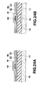
- FIG. 24A is an explanatory diagram showing a manufacturing step of a thin film transistor of embodiment 2;
- FIG. 24B is an explanatory diagram showing a manufacturing step of a thin film transistor of embodiment 2;
- FIG. 25A is an explanatory diagram showing a manufacturing step of a thin film transistor of embodiment 2;
- FIG. 25B is an explanatory diagram showing a manufacturing step of a thin film transistor of embodiment 2;
- FIG. 26A is an explanatory diagram showing a manufacturing step of a thin film transistor of embodiment 2;
- FIG. 26B is an explanatory diagram showing a manufacturing step of a thin film transistor of embodiment 2;
- FIG. 27A is an explanatory diagram showing a manufacturing step of a thin film transistor of embodiment 2;
- FIG. 27B is an explanatory diagram showing a manufacturing step of a thin film transistor of embodiment 2;
- FIG. 28A is an explanatory diagram showing a manufacturing step of a thin film transistor of embodiment 2.
- FIG. 28B is an explanatory diagram showing a manufacturing step of a thin film transistor of embodiment 2;
- FIG. 29A is an explanatory diagram showing a manufacturing step of a thin film transistor of embodiment 2.
- FIG. 29B is an explanatory diagram showing a manufacturing step of a thin film transistor of embodiment 2.
- FIG. 30A is an explanatory diagram showing a manufacturing step of a thin film transistor of embodiment 2;
- FIG. 30B is an explanatory diagram showing a manufacturing step of a thin film transistor of embodiment 2;
- FIG. 31A is an explanatory diagram showing a manufacturing step of a thin film transistor of embodiment 2;
- FIG. 31B is an explanatory diagram showing a manufacturing step of a thin film transistor of embodiment 2;
- FIG. 32 is a planar view showing one pixel of an EL panel of embodiment 3;
- FIG. 33 is a cross sectional view of a plane along arrows XXXIII-XXXIII shown in FIG. 32 ;
- FIG. 34 is a cross sectional view of a plane along arrows XXXIV-XXXIV shown in FIG. 32 ;
- FIG. 35A is an explanatory diagram showing a manufacturing step of a thin film transistor of embodiment 3.
- FIG. 35B is an explanatory diagram showing a manufacturing step of a thin film transistor of embodiment 3.
- FIG. 36A is an explanatory diagram showing a manufacturing step of a thin film transistor of embodiment 3.
- FIG. 36B is an explanatory diagram showing a manufacturing step of a thin film transistor of embodiment 3.
- FIG. 37A is an explanatory diagram showing a manufacturing step of a thin film transistor of embodiment 3.
- FIG. 37B is an explanatory diagram showing a manufacturing step of a thin film transistor of embodiment 3.
- FIG. 38A is an explanatory diagram showing a manufacturing step of a thin film transistor of embodiment 3.
- FIG. 38B is an explanatory diagram showing a manufacturing step of a thin film transistor of embodiment 3.
- FIG. 39A is an explanatory diagram showing a manufacturing step of a thin film transistor of embodiment 3.
- FIG. 39B is an explanatory diagram showing a manufacturing step of a thin film transistor of embodiment 3.
- FIG. 40A is an explanatory diagram showing a manufacturing step of a thin film transistor of embodiment 3.
- FIG. 40B is an explanatory diagram showing a manufacturing step of a thin film transistor of embodiment 3.
- FIG. 41A is an explanatory diagram showing a manufacturing step of a thin film transistor of embodiment 3.
- FIG. 41B is an explanatory diagram showing a manufacturing step of a thin film transistor of embodiment 3.
- FIG. 42A is an explanatory diagram showing a manufacturing step of a thin film transistor of embodiment 3.
- FIG. 42B is an explanatory diagram showing a manufacturing step of a thin film transistor of embodiment 3.
- FIG. 43A is an explanatory diagram showing a manufacturing step of a thin film transistor of embodiment 3.
- FIG. 43B is an explanatory diagram showing a manufacturing step of a thin film transistor of embodiment 3.
- FIG. 44 is a planar view showing one pixel of an EL panel of embodiment 4.
- FIG. 45 is a cross sectional view of a plane along arrows XLV-XLV shown in FIG. 44 ;
- FIG. 46 is a cross sectional view of a plane along arrows XLVI-XLVI shown in FIG. 44 ;
- FIG. 47A is an explanatory diagram showing a manufacturing step of a thin film transistor of embodiment 4.
- FIG. 47B is an explanatory diagram showing a manufacturing step of a thin film transistor of embodiment 4.
- FIG. 48A is an explanatory diagram showing a manufacturing step of a thin film transistor of embodiment 4.
- FIG. 48B is an explanatory diagram showing a manufacturing step of a thin film transistor of embodiment 4.
- FIG. 49A is an explanatory diagram showing a manufacturing step of a thin film transistor of embodiment 4.
- FIG. 49B is an explanatory diagram showing a manufacturing step of a thin film transistor of embodiment 4.
- FIG. 50A is an explanatory diagram showing a manufacturing step of a thin film transistor of embodiment 4.
- FIG. 50B is an explanatory diagram showing a manufacturing step of a thin film transistor of embodiment 4.
- FIG. 51A is an explanatory diagram showing a manufacturing step of a thin film transistor of embodiment 4.
- FIG. 51B is an explanatory diagram showing a manufacturing step of a thin film transistor of embodiment 4.
- FIG. 52A is an explanatory diagram showing a manufacturing step of a thin film transistor of embodiment 4.
- FIG. 52B is an explanatory diagram showing a manufacturing step of a thin film transistor of embodiment 4.
- FIG. 53A is an explanatory diagram showing a manufacturing step of a thin film transistor of embodiment 4.
- FIG. 53B is an explanatory diagram showing a manufacturing step of a thin film transistor of embodiment 4.
- FIG. 54A is an explanatory diagram showing a manufacturing step of a thin film transistor of embodiment 4.
- FIG. 54B is an explanatory diagram showing a manufacturing step of a thin film transistor of embodiment 4.
- FIG. 55A is an explanatory diagram showing a manufacturing step of a thin film transistor of embodiment 4.
- FIG. 55B is an explanatory diagram showing a manufacturing step of a thin film transistor of embodiment 4.
- FIG. 56 is a front view showing an example of a cellular phone employing an EL panel as a display panel
- FIG. 57A is a front perspective view showing an example of a digital camera employing an EL panel as a display panel;
- FIG. 57B is a rear perspective view showing an example of a digital camera employing an EL panel as a display panel;
- FIG. 58 is a perspective view showing an example of a personal computer employing an EL panel as a display panel
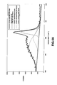
- FIG. 59 is a diagram for explaining a method of measuring degree of crystallization of a semiconductor by Raman spectrometric method.
- FIG. 60 is a circuit diagram showing another circuit corresponding to one pixel of an EL panel.
- FIG. 1 is a planar view showing an arrangement structure of a plurality of pixels P in an EL panel 1 which is a light emitting apparatus.
- FIG. 2 is a planar view showing a schematic structure of the EL panel 1 .
- a plurality of pixels P are arranged in a predetermined pattern in a matrix form on the EL panel 1 .
- the plurality of pixels P include a red pixel P which emits light of R (red), green pixel P which emits light of G (green) and blue pixel P which emits light of B (blue).
- a plurality of scanning lines 2 are arranged along a row direction so as to be substantially parallel to each other, and a plurality of signal lines 3 are arranged along a column direction so as to be substantially parallel to each other and to be substantially orthogonal to the scanning lines 2 from a planar view.
- Voltage supplying lines 4 are provided along the scanning lines 2 in between adjacent scanning lines 2 . The portion surrounded by two adjacent scanning lines 2 and two adjacent signal lines 3 correspond to pixel P.
- Bank 13 which is a partition wall, is provided so as to cover above scanning lines 2 , signal lines 3 and voltage supplying lines 4 on the EL panel 1 .
- Bank 13 is provided in, for example, a grid like shape, and a plurality of opening sections 13 a surrounded by the bank 13 in a substantial rectangular shape are formed for each pixel P.
- a predetermined carrier transporting layer (later described hole injecting layer 8 b and light emitting layer 8 c ) is provided in the opening section 13 a of the bank 13 and this is to be a light emitting portion of the pixel P.
- the carrier transporting layer is a layer which transports a hole or an electron by applying voltage.
- the bank 13 is not limited to the above, and instead of providing an opening section 13 a for each pixel P, the bank 13 can cover the signal line 3 and extend along a column direction and include an opening section in a stripe shape which collectively exposes a center section of each later described pixel electrode 8 a of the plurality of pixels P aligned in a column direction.
- FIG. 3 is a circuit diagram showing an example of a circuit corresponding to one pixel of the EL panel 1 which is driven by an active matrix driving method.
- the EL panel 1 is provided with the scanning line 2 , the signal line 3 which intersects with scanning line 2 and voltage supplying line 4 along the scanning line 2 .
- Each pixel of the EL panel 1 is provided with a switch transistor 5 which is a second thin film transistor, a driving transistor 6 which is a first thin film transistor, a capacitor 7 , and an EL element 8 which is a light emitting element.
- the switch transistor 5 and the driving transistor 6 function as driving elements which allow the EL element 8 to emit light.
- a gate of the switch transistor 5 is connected to the scanning line 2 , either one of a drain or a source of the switch transistor 5 is connected to the signal line 3 , the other of either of the drain or the source of the switch transistor 5 is connected to one of an electrode of the capacitor 7 and a gate of the driving transistor 6 .
- Either one of a drain or a source of the driving transistor 6 is connected to the voltage supplying line 4 and the other of either of the drain or the source of the driving transistor 6 is connected to the other electrode of the capacitor 7 and an anode of the EL element 8 . All cathodes of the EL element 8 of the pixel P are maintained at a constant voltage Vcom (for example, grounded).
- each scanning line 2 is connected to a scanning driver in a periphery of the EL panel 1
- each voltage supplying line 4 is connected to a voltage source which outputs a constant voltage or a voltage driver which suitably outputs a voltage signal
- each signal line 3 is connected to a data driver
- the EL panel 1 is driven by an active matrix driving method using these drivers.
- the constant voltage from the voltage source or the voltage signal from the voltage driver is supplied to the voltage supplying line 4 .
- FIG. 4 is a planar view corresponding to one pixel P of the EL panel 1
- FIG. 5 is a cross sectional view of a plane along arrows V-V shown in FIG. 4
- FIG. 6 is a cross sectional view of a plane along arrows VI-VI shown in FIG. 4
- FIG. 4 mainly shows electrodes and lines.
- the transistor structure 56 of each pixel P includes the switch transistor 5 and the driving transistor 6 .
- the switch transistor 5 and the driving transistor 6 are arranged along the signal line 3 , the capacitor 7 is positioned near the switch transistor 5 and the EL element 8 is positioned near the driving transistor 6 .
- the switch transistor 5 , the driving transistor 6 , the capacitor 7 and the EL element 8 are positioned between the scanning line 2 and the voltage supplying line 4 .
- a first gate electrode 6 a is provided on the substrate 10 , and a first insulating film 11 is formed on an upper surface of the substrate 10 so as to cover the first gate electrode 6 a .
- a second semiconductor film 5 b and a first semiconductor film 6 b On the first insulating film 11 , a second semiconductor film 5 b and a first semiconductor film 6 b , a pair of impurity semiconductor films 5 f , 5 g , 6 f and 6 g , and drain electrodes 5 h and 6 h and source electrodes 5 i and 6 i are each formed on a predetermined position, and a second insulating film 12 is formed so as to cover the drain electrodes 5 h and 6 h and the source electrodes 5 i and 6 i .
- a second gate electrode 5 a is provided on the second insulating film 12 and a passivation film 14 is formed on the upper surface of the second insulating film 12 so as to cover the second gate electrode 5 a.
- the signal line 3 is formed between the substrate 10 and the first insulating film 11 .
- the scanning line 2 is formed between the second insulating film 12 and the passivation film 14 .
- the voltage supplying line 4 is formed on the first insulating film 11 .
- a groove (not shown) is formed along the voltage supplying line 4 on the part of the second insulating film 12 on the voltage supplying line 4 , and a conducting layer 4 a which covers the voltage supplying line 4 is provided in the groove.
- the switch transistor 5 is a second thin film transistor with a top gate structure.
- the switch transistor 5 includes a second gate electrode 5 a , a second semiconductor film 5 b , a protective insulating film 5 d , impurity semicondutor films 5 f , 5 g , drain electrode 5 h , source electrode 5 i , and the like.
- the first insulating film 11 with insulating properties formed on the upper surface of the substrate 10 includes, for example, light permeability and includes silicon nitride or silicon oxide.
- An intrinsic second semiconductor film 5 b is formed on the first insulating film 11 in a position which is to correspond with the second gate electrode 5 a.
- the second semiconductor film 5 b includes, for example, crystalline silicon, especially microcrystalline silicon and includes a first portion 51 positioned on the first insulating film 11 side and a second portion 52 positioned on the opposite surface side (second gate electrode 5 a side).
- degree of crystallization of silicon of the first portion 51 is formed higher than the second portion 52 .
- the degree of crystallization of silicon is relatively higher compared to the second portion 52 , and the rate of the crystalline silicon portion is higher than the second portion 52 .
- the rate of the amorphous silicon portion is large compared to the first portion 51 , and preferably, the second portion 52 of the second semiconductor film 5 b is a portion with substantially only amorphous silicon.
- the second semiconductor film 5 b is a channel portion where a channel is formed.
- a protective insulating film 5 d with insulating properties is formed on a center section of the second semiconductor film 5 b.
- the protective insulating film 5 d includes, for example, silicon nitride or silicon oxide.
- an impurity semiconductor film 5 f is formed so that a part overlaps with the protective insulating film 5 d
- an impurity semiconductor film 5 g is formed so that a part overlaps with the protective insulating film 5 d .
- the impurity semiconductor films 5 f and 5 g are formed apart from each other on each edge side of the second semiconductor film 5 b .
- the impurity semiconductor films 5 f and 5 g are n-type semiconductors including n-type impurity, however, it is not limited to the above, and when the switch transistor 5 is a p-type transistor, a p-type semiconductor can be used.
- the drain electrode 5 h is formed on the impurity semiconductor film 5 f .
- the source electrode 5 i is formed on the impurity semiconductor film 5 g . It is preferable that the drain electrode 5 h and the source electrode 5 i are formed from material selected from, for example, a Cr film, an Al film, a Cr/Al laminated film, an AlTi alloy film, and an AlTiNd alloy film.
- the second insulating film 12 includes, for example, silicon nitride or silicon oxide.
- the second gate electrode 5 a is formed on the second insulating film 12 in a position corresponding to the protective insulating film 5 d . It is preferable that this second gate electrode 5 a is formed from material selected from, for example, a Cr film, an Al film, a Cr/Al laminated film, an AlTi alloy film or an AlTiNd alloy film.
- the second gate electrode 5 a on the second insulating film 12 is covered by the passivation film 14 .
- the passivation film 14 includes, for example, silicon nitride or silicon oxide.
- the switch transistor 5 is covered by the passivation film 14 .
- the second insulating film 12 and the protective insulating film 5 d function as a gate insulating film, and a channel (channel portion) is formed in the portion of the second semiconductor film 5 b covered by the protective insulating film 5 d and acted on by the electric field of the second gate electrode 5 a .
- a channel is formed in a second portion 52 of the second semiconductor film 5 b which is the second gate electrode 5 a side of the second semiconductor film 5 b , and the second portion 52 is the electric current path between the source electrode 5 i and the drain electrode 5 h.
- the second portion 52 of the second semiconductor film 5 b is a semiconductor layer including more amorphous silicon and the switch transistor 5 which uses the second portion 52 as the electric current path of the channel corresponds to a thin film transistor including a semiconductor film made from amorphous silicon (or a semiconductor film including amorphous silicon as a main component).
- the leak current is smaller in the amorphous silicon of the second portion 52 of the switch transistor 5 compared to the crystalline silicon such as microcrystalline silicon and (electric current which flows in the semiconductor layer when on)/(electric current which flows in the semiconductor layer when off) is high. Therefore, the above suitably functions as the switch transistor which controls the on/off of the driving transistor 6 .
- the driving transistor 6 is a first thin film transistor with a bottom gate structure.
- the driving transistor 6 includes a first gate electrode 6 a , a first semiconductor film 6 b , a protective insulating film 6 d , impurity semiconductor films 6 f and 6 g , drain electrode 6 h , source electrode 6 i and the like.
- the first gate electrode 6 a is formed between the substrate 10 and the first insulating film 11 . It is preferable that the first gate electrode 6 a is formed from material selected from, for example, a Cr film, an Al film, a Cr/Al laminated film, an AlTi alloy film and an AlTiNd alloy film.
- the first insulating film 11 with insulating properties is formed on the first gate electrode 6 a and the first gate electrode 6 a is covered by the first insulating film 11 .
- the intrinsic first semiconductor film 6 b is formed in a position on the first insulating film 11 corresponding to the first gate electrode 6 a .
- the first semiconductor film 6 b faces the first gate electrode 6 a with the first insulating film 11 in between.
- the first semiconductor film 6 b includes, for example, crystalline silicon, specifically, microcrystalline silicon and includes a first portion 61 positioned on the first insulating film 11 side (first gate electrode 6 a side) and a second portion 62 positioned on the opposite surface side.
- degree of crystallization of silicon of the first portion 61 is formed higher compared to the second portion 62 .
- degree of crystallization of silicon is relatively higher compared to the second portion 62
- the rate of the crystalline silicon portion is higher compared to the second portion 62 .
- the rate of the portion of the amorphous silicon is higher compared to the first portion 61 , and preferably the second portion 62 of the first semiconductor film 6 b is a portion with substantially only amorphous silicon.
- the first portion 61 of the first semiconductor film 6 b and the first portion 51 of the second semiconductor film 5 b have the same composition and have the same thickness.
- the second portion 62 of the first semiconductor film 6 b and the second portion 52 of the second semiconductor film 5 b have the same composition and have the same thickness. Therefore, as described later, the first semiconductor film 6 b and the second semiconductor film 5 b can be manufactured collectively with the same process using the semiconductor layer 9 which is a layer with the same material.
- the first semiconductor film 6 b is a channel portion where the channel is formed.
- the protective insulating film 6 d with insulating properties is formed on a center section of the first semiconductor film 6 b .
- the protective insulating film 6 d and the protective insulating film 5 d are composed of the same material and have the same thickness, and preferably include, for example, silicon nitride or silicon oxide. Therefore, as described later, the protective insulating film 6 d and the protective insulating film 5 d can be manufactured collectively with the same process using the protective insulating layer 9 d which is a layer with the same material.
- the impurity semiconductor film 6 f is formed so that a part overlaps with the protective insulating film 6 d
- the impurity semiconductor film 6 g is formed so that a part overlaps with the protective insulating film 6 d .
- the impurity semiconductor films 6 f and 6 g are formed apart on each edge side of the first semiconductor film 6 b .
- the impurity semiconductor films 6 f and 6 g are n-type semiconductors including n-type impurity, however it is not limited to the above, and when the switch transistor 5 and the driving transistor 6 are p-type transistors, a p-type semiconductor can be used.
- the impurity semiconductor films 6 f and 6 g and the impurity semiconductor films 5 f and 5 g are composed of the same material and have the same thickness. As described later, the impurity semiconductor films 6 f and 6 g and the impurity semiconductor films 5 f and 5 g can be manufactured collectively with the same process using the impurity semiconductor layer 9 f which is a layer with the same material.
- the drain electrode 6 h is formed on the impurity semiconductor film 6 f .
- the source electrode 6 i is formed on the impurity semiconductor film 6 g . It is preferable that the drain electrode 6 h and the source electrode 6 i are formed from material selected from, for example, a Cr film, an Al film, a Cr/Al laminated film, an AlTi alloy film and an AlTiNd alloy film.
- the drain electrode 6 h , the source electrode 6 i , the drain electrode 5 h and the source electrode 5 i are composed of the same material and have the same thickness. As described later, the drain electrode 6 h , the source electrode 6 i , the drain electrode 5 h and the source electrode 5 i can be manufactured collectively with the same process using the conducting film 9 h which is a layer with the same material.
- a second insulating film 12 with insulating properties is formed on the protective insulating film 6 d , the drain electrode 6 h and the source electrode 6 i , and the protective insulating film 6 d , the drain electrode 6 h , the source electrode 6 i , etc. are covered by the second insulating film 12 . Therefore, the second insulating film 12 covers both the switch transistor 5 and the driving transistor 6 . Moreover, the passivation film 14 is formed on the second insulating film 12 corresponding to the driving transistor 6 , and the passivation film 14 covers both the switch transistor 5 and the driving transistor 6 .
- the driving transistor 6 is covered by both the second insulating film 12 and the passivation film 14 .
- the first insulating film 11 functions as a gate insulating film, and a channel (channel portion) is formed in the portion of the first semiconductor film 6 b covered by the protective insulating film 6 d and acted on by the electric field of the first gate electrode 6 a .
- a channel is formed in a first portion 61 of the first semiconductor film 6 b which is the first gate electrode 6 a side of the first semiconductor film 6 b , and the first portion 61 is the electric current path between the source electrode 6 i and the drain electrode 6 h.
- the first portion 61 of the first semiconductor film 6 b is a semiconductor layer including more crystalline silicon than the second portion 62 . Therefore, the driving transistor 6 which uses the first portion 61 as the electric current path of the channel corresponds to a thin film transistor including a semiconductor film made from crystalline silicon (or a semiconductor film including crystalline silicon as the main component).
- the microcrystalline silicon in the first portion 61 of the driving transistor 6 is crystalline silicon with a grain diameter of about 50 to 100 nm. Therefore, the shift of threshold voltage by the driving of the transistor is small compared to the amorphous silicon and the deterioration of the transistor can be suppressed.
- the degree of carrier mobility is high, and therefore suitably functions as a driving transistor which flows electric current in the EL element 8 by control of the switch transistor 5 .
- the capacitor 7 is connected between the first gate electrode 6 a and the source electrode 6 i of the driving transistor 6 .
- the electrode 7 a of the capacitor 7 is connected to the first gate electrode 6 a of the driving transistor 6
- the electrode 7 b of the capacitor 7 is connected to the source electrode 6 i of the driving transistor 6 .
- one electrode 7 a of the capacitor 7 is formed between the substrate 10 and the first insulating film 11
- the other electrode 7 b of the capacitor 7 is formed between the first insulating film 11 and the second insulating film 12 .
- the electrode 7 a and the electrode 7 b face each other with the first insulating film 11 , which is a dielectric material, in between.
- the signal line 3 , the electrode 7 a of the capacitor 7 , and the first gate electrode 6 a of the driving transistor 6 are collectively formed by processing the shape of a conducting film formed on an entire surface of the substrate 10 by photolithography, etching, etc.
- the voltage supplying line 4 , the electrode 7 b of the capacitor 7 , the drain electrode 5 h and the source electrode 5 i of the switch transistor 5 , and the drain electrode 6 h and the source electrode 6 i of the driving transistor 6 are collectively formed by processing the shape of a conducting film formed on an entire surface of the first insulating film 11 by photolithography, etching, etc.
- the scanning line 2 , the second gate electrode 5 a of the switch transistor 5 and the conducting layer 4 a are collectively formed by processing the shape of a conducting film formed on an entire surface of the second insulating film 12 by photolithography, etching, etc.
- a contact hole 11 b is formed on a portion where the drain electrode 5 h and the signal line 3 overlaps
- a contact hole 11 c is formed on a portion where the first gate electrode 6 a and the source electrode 5 i overlaps
- contact plugs 20 b and 20 c are implanted in the contact holes 11 b and 11 c .
- the drain electrode 5 h of the switch transistor 5 and the signal line 3 are electrically conducted by the contact plug 20 b .
- the source electrode 5 i of the switch transistor 5 and the electrode 7 a of the capacitor 7 as well as the source electrode 5 i of the switch transistor 5 and the first gate electrode 6 a of the driving transistor 6 are electrically conducted by the contact plug 20 c .
- the drain electrode 5 h can be conducted with the signal line 3 by direct contact and the source electrode 5 i can be conducted with the first gate electrode 6 a by direct contact without using the contact plugs 20 b and 20 c.
- the first gate electrode 6 a of the driving transistor 6 is connected as one with the electrode 7 a of the capacitor 7
- the drain electrode 6 h of the driving transistor 6 is connected as one with the voltage supplying line 4
- the source electrode 6 i of the driving transistor 6 is connected as one with the electrode 7 b of the capacitor 7 .
- the pixel electrode 8 a is provided on the substrate 10 with the first insulating film 11 in between, and a separate pixel electrode 8 a is formed for each pixel P.
- the pixel electrode 8 a is a transparent electrode, and it is preferable that the pixel electrode 8 a is formed from material selected from for example, tin doped indium oxide (ITO), zinc doped indium oxide, indium oxide (In 2 O 2 ), tin oxide (SnO 2 ), zinc oxide (ZnO) and cadmium-tin oxide (CTO).
- the pixel electrode 8 a is a laminated structure including a light reflecting layer as a lower layer which is a single or alloy layer of aluminum, etc. with high light reflecting properties, and the above described transparent electrode as the upper layer.
- a part of the pixel electrode 8 a overlaps with the source electrode 6 i of the driving transistor 6 , and the pixel electrode 8 a and the source electrode 6 i are connected to each other.
- the second insulating film 12 and the passivation film 14 are formed so as to cover the scanning line 2 , the signal line 3 , the voltage supplying line 4 , the switch transistor 5 , the driving transistor 6 , the periphery of the pixel electrode 8 a , the electrode 7 b of the capacitor 7 and the first insulating film 11 .
- the opening section 12 a is formed in the second insulating film 12 and the passivation film 14 so as to expose the center section of each pixel electrode 8 a . Therefore, the second insulating film 12 and the passivation film 14 are formed in a grid like shape from a planar view.
- the EL element 8 includes the pixel electrode 8 a as the first electrode which is to be the anode, the hole injecting layer 8 b which is a compound film formed on the pixel electrode 8 a , the light emitting layer 8 c which is a compound film formed on the hole injecting layer 8 b , and the counter electrode 8 d as the second electrode formed on the light emitting layer 8 c .
- the counter electrode 8 d is a single electrode common to all pixels P and is formed continuously on all pixels P.
- the hole injecting layer 8 b is a layer including, for example PEDOT (polyethylenedioxythiophene) which is a conductive polymer and PSS (polystyrene sulfonate) which is a dopant and is a carrier injecting layer to inject a hole from the pixel electrode 8 a to the light emitting layer 8 c.
- PEDOT polyethylenedioxythiophene
- PSS polystyrene sulfonate
- the light emitting layer 8 c includes material which emits light of either R (red), G (green) or B (blue) in each pixel, and is a layer including light emitting material of polyfluorene series or polyphenylene vinylene series and emits light by recombination between an electron supplied from the counter electrode 8 d and a hole injected from the hole injecting layer 8 b . Therefore, among the pixel P which emits light of R (red), the pixel P which emits light of G (green) and the pixel P which emits light of B (blue), the light emitting material of the light emitting layer 8 c are different from each other.
- the pixels P which are R (red), G (green) and B (blue) are aligned in a stripe pattern in which, for example, the same color pixel is aligned in the vertical direction.
- This alignment pattern is not limited to a stripe pattern and can be a delta sequence.
- the opening section 13 a of the bank 13 is provided in a grid like shape along the alignment pattern of each pixel P or in a stripe shape along a column direction so that a plurality of the center sections of the pixel electrode 8 a of the pixel P are collectively exposed.
- the counter electrode 8 d is formed from material with a lower work function than the pixel electrode 8 a , and when the counter electrode 8 d is employed as the cathode, the counter electrode 8 d is formed for example as a laminated body including a lower layer of a single body or alloy including at least one type of indium, magnesium, calcium, lithium, barium, or rare earth metal and an upper layer in order to reduce sheet resistance.
- the upper layer is a transparent electrode and it is preferable that the upper layer is formed from material selected from, for example, tin doped indium oxide (ITO), zinc doped indium oxide, indium oxide (In 2 O 3 ), tin oxide (SnO 2 ), zinc oxide (ZnO), and cadmium-tin oxide (CTO).
- ITO tin doped indium oxide
- the upper layer is a single or alloy layer of aluminum, etc. with high light reflecting properties.
- the counter electrode 8 d is an electrode common to all pixels P and covers the later described bank 13 with a compound film such as the light emitting layer 8 c.
- the light emitting layer 8 c which is to be the light emitting part is divided with respect to each pixel P by the second insulating film 12 and the bank 13 .
- the hole injecting layer 8 b and the light emitting layer 8 c as the carrier transporting layers are layered on the pixel electrode 8 a .
- the hole injecting layer 8 b can be formed continuously to spread on a plurality of pixels P. In this case, it is preferable to use germanium oxide with hole injecting properties.
- the bank 13 functions as a partition wall to prevent the liquid body in which material which is to be the hole injecting layer 8 b or the light emitting layer 8 c is dissolved or dispersed in a solvent from flowing into the adjacent pixel P through the bank 13 .
- the bank 13 covers the entire second insulating film 12 .
- the opening section 13 a is wider than the opening section 12 a , and the side face of the opening edge of the opening section 12 a of the second insulating film 12 can be exposed from the opening section 13 a of the bank 13 .
- the liquid body including the material which is to be the hole injecting layer 8 b is applied on each pixel electrode 8 a surrounded by each opening section 13 a , and the substrate 10 is heated as a whole, to dry the liquid body to form the compound film.
- This compound film is to be the hole injecting layer 8 b which is the first carrier transporting layer.
- the liquid body including the material which is to be the light emitting layer 8 c is applied on each hole injecting layer 8 b surrounded by each opening section 13 a , and the substrate 10 is heated as a whole, to dry the liquid body to form the compound film.
- This compound film is to be the light emitting layer 8 c which is the second carrier transporting layer.
- the counter electrode 8 d is provided so as to cover the light emitting layer 8 c and the bank 13 .
- the pixel electrode 8 a , the substrate 10 and the first insulating film 11 are transparent, and the light emitted from the light emitting layer 8 c transmits the pixel electrode 8 a , the first insulating film 11 and the substrate 10 and exits. Therefore, the rear surface of the substrate 10 is to be the display surface.
- the structure can be a top emission structure in which instead of the substrate 10 side, the opposite side is to be the display surface.
- the counter electrode 8 d is to be the transparent electrode
- the pixel electrode 8 a is to be the reflecting electrode and the light emitted from the light emitting layer 8 c transmits the counter electrode 8 d and exits.
- This EL panel 1 is driven and emits light as described in the following.
- the data driver applies a voltage of a level according to the tone to all signal lines 3 when each scanning line 2 is selected, since the switch transistor 5 of each pixel P corresponding to the selected scanning line 2 is turned on, the voltage of the signal line 3 is applied to the gate electrode 6 a of the driving transistor 6 .
- the potential difference between the gate electrode 6 a and the source electrode 6 i of the driving transistor 6 is determined, the amount of the drain-source electric current in the driving transistor 6 is determined, and the EL element 8 emits light of a brightness according to the drain-source electric current of the EL element 8 .
- the switch transistor 5 is turned off, the electronic charge based on the voltage applied to the gate electrode 6 a of the driving transistor 6 is stored in the capacitor 7 and the potential difference between the gate electrode 6 a and the source electrode 6 i of the driving transistor 6 is maintained. Therefore, the driving transistor 6 flows the drain-source electric current with the same electric current value as the time of selection, and the brightness of the EL element 8 is maintained.
- the switch transistor 5 switches the voltage applied to the gate electrode 6 a of the driving transistor 6 to the voltage of the predetermined tone level applied to the signal line 3 , the driving transistor 6 flows the drain-source electric current (driving electric current) of the electric current value according to the level of the voltage applied to the gate electrode 6 a from the voltage supplying line 4 to the EL element 8 , and the EL element 8 emits light at a predetermined tone according to the electric current value (electric current density).
- the EL element 8 emits light by driving and control of the transistor structure 56 including the switch transistor 5 and the driving transistor 6 , and the EL panel 1 emits light.
- FIG. 7A and FIG. 7B the manufacturing method of the switch transistor 5 and the driving transistor 6 composing the transistor structure 56 in the EL panel 1 of the present invention is described using FIG. 7A and FIG. 7B to FIG. 17A and FIG. 17B showing each process.
- each thin film transistor is shown to be the same size and the main section of each thin film transistor is schematically illustrated and explained.
- FIG. A of each number shows the driving transistor 6
- FIG. B of each number shows the switch transistor 5 .
- a gate metal layer including, for example, a Cr film, an Al film, a Cr/Al laminated film, an AlTi alloy film or an AlTiNd alloy film, etc. is accumulated on the substrate 10 by sputtering and patterned by photolithography, etching, etc. to form the first gate electrode 6 a of the driving transistor 6 .
- the signal line 3 and the electrode 7 a of the capacitor 7 are formed on the substrate 10 with the first gate electrode 6 a (see FIG. 5 and FIG. 6 ).
- the first insulating film 11 such as silicon nitride, etc. is formed by plasma CVD (PE-CVD).
- the semiconductor layer 9 b including crystalline silicon is formed on the first insulating film 11 by plasma CVD.
- the semiconductor layer 9 b which is to be the semiconductor film ( 5 b , 6 b ) is formed, the first silicon layer 91 with a relatively high degree of crystallization of silicon is formed first, and then a second silicon layer 92 with a relatively low degree of crystallization of silicon is formed.
- the second silicon layer 92 is substantially only amorphous silicon.
- the first silicon layer 91 is formed after plasma degradation of SiH 4 gas and H 2 gas, and by setting the rate of the H 2 gas overwhelmingly larger compared to the SiH 4 gas and by making the plasma power and the pressure large to raise the degree of crystallization, the first silicon layer 91 which is a microcrystalline silicon thin film can be formed.
- the surface of the first silicon layer 91 which is the microcrystalline silicon thin film tends to be uneven.
- the second silicon layer 92 which is the amorphous silicon thin film is layered on the first silicon layer 91 , the unevenness of the surface of the first silicon layer 91 is covered and moderated by the second silicon layer 92 .
- the first silicon layer 91 can be formed by a method of emitting laser light to the amorphous silicon thin film to be reformed to the microcrystalline silicon thin film.
- the substrate is taken out of the chamber of the CVD apparatus and laser light emitting processing is performed to form the first silicon layer 91 , and then the substrate is put in the chamber of the CVD apparatus again to layer the second silicon layer 92 on the first silicon layer 91 .
- the degree of crystallization of silicon of the first silicon layer 91 and the second silicon layer 92 in the semiconductor layer 9 b can be determined based on the degree of crystallization calculated by, for example, raman spectrophotometry.
- amorphous silicon provides a spectrum including a broad peak at around 480 cm ⁇ 1 .
- the very minute crystalline silicon of the grain boundary or with a crystal diameter of 5 nm or less provides a spectrum including a broad peak at around 500 cm ⁇ 1 .
- the crystallized silicon provides a spectrum including a relatively sharp peak at around 520 cm ⁇ 1 .
- the spectrum of the silicon thin film of the first silicon layer 91 and the second silicon layer 92 which is the object of measurement can be represented by combining, for example, as shown in FIG. 59 , each component spectrum, in other words, each spectrum of amorphous silicon, very minute crystalline silicon of the grain boundary or with a crystal diameter of 5 nm or less, and crystallized silicon, at a certain ratio.
- each component spectrum in other words, each spectrum of amorphous silicon, very minute crystalline silicon of the grain boundary or with a crystal diameter of 5 nm or less, and crystallized silicon, at a certain ratio.
- the degree of crystallization d (%) can be calculated by the following formula 1 when the intensity of the component spectrum of the amorphous silicon is I a-Si , the intensity of the component spectrum of the very minute crystalline silicon of the grain boundary or with a crystal diameter of 5 nm or less is I uc-Si and the intensity of the component spectrum of the crystallized silicon is I c-Si , included in a spectrum of a silicon thin film.
- d (%) ( I c-Si +I uc-Si )/( I c-Si +I uc-Si +I a-Si ) ⁇ 100 (1)
- the degree of crystallization is 20% or more, it is defined to be a microcrystalline silicon thin film, and when the degree of crystallization is less than 20%, it is defined to be an amorphous silicon thin film.
- preprocessing of forming the semiconductor layer 9 b on the first insulating film 11 it is preferable to perform plasma processing on the surface of the first insulating film 11 .
- the plasma processing is performed on the first insulating film 11 , the surface of the first insulating film 11 is reformed, and the degree of crystallization of the crystalline silicon formed on the first insulating film 11 can be raised.
- the plasma processing of the present embodiment can be performed under conditions such as using N 2 O gas, setting the gas flow rate to 2000 [SCCM], setting the power density to 0.356 [W/cm 2 ] and setting the pressure to 80 [Pa].
- N 2 O gas is used, however, instead of N 2 O gas, oxygen gas or hydrogen gas can be used under suitable conditions.
- the protective insulating layer 9 d such as silicon nitride is formed on the semiconductor layer 9 b (second silicon layer 92 ) by the CVD method, etc.
- the protective insulating layer 9 d is patterned by photolithography, etching, etc. and the protective insulating film 6 d of the driving transistor 6 and the protective insulating film 5 d of the switch transistor 5 , which cover the portion which is to be the channel on the semiconductor layer 9 b , are formed.
- the first silicon layer 91 is covered by the second silicon layer 92 , when the protective insulating layer 9 d is patterned by etching, the first silicon layer 91 is not subjected to the etching environment, and therefore, the first silicon layer 91 of the semiconductor layer 9 b does not receive damage such as reduction of film.
- the semiconductor layer is a single layer of a crystalline silicon (specifically microcrystalline silicon)
- the etching gas may pass the sunken part of the crystalline silicon and reach the first insulating film under the semiconductor layer, and a part of the first insulating film may be scraped.
- the semiconductor layer 9 b of the present embodiment the second silicon layer 92 of the amorphous silicon thin film is layered on the first silicon layer 91 of the microcrystalline silicon thin film, and the unevenness of the first silicon layer 91 is covered. Therefore, the semiconductor layer 9 b and the first insulating film 11 are not damaged by etching and the protective insulating film 6 d of the driving transistor 6 and the protective insulating film 5 d of the switch transistor 5 can be favorably formed.
- the impurity semiconductor layer 9 f which is to be the impurity semiconductor film is formed by sputtering or CVD method on the semiconductor layer 9 b on which the protective insulating films 6 d and 5 d are formed.
- the material used as the impurity semiconductor layer 9 f is different according to whether the switch transistor 5 and the driving transistor 6 are p-type or n-type.
- the layer is formed by forming a film of plasma mixing an acceptor type impurity such as diborane, etc. in SiH 4 gas.
- the layer is formed by forming a film of plasma by mixing a donor type impurity such as arsine, phosphine, etc. in the SiH 4 gas.
- the conducting film 9 h which is to be the source electrode and the drain electrode is formed by, for example, sputtering on the impurity semiconductor layer 9 f.
- the conducting film 9 h is patterned by photolithography, etching, etc. and the source electrode 6 i and the drain electrode 6 h of the driving transistor 6 , the source electrode 5 i and the drain electrode 5 h of the switch transistor 5 are formed, and moreover, the voltage supplying line 4 , and the electrode 7 b of the capacitor 7 are also formed. (see FIG. 4 , FIG. 5 and FIG. 6 ).
- the source electrode 6 i and the drain electrode 6 h and the source electrode 5 i and the drain electrode 5 h are used as a mask and the impurity semiconductor layer 9 f and the semiconductor layer 9 b are patterned by dry etching and the impurity semiconductor films 6 f and 6 g and the first semiconductor film 6 b , and the impurity semiconductor films 5 f and 5 g and the second semiconductor film 5 b are formed.
- the first semiconductor film 6 b includes the first portion 61 and the second portion 62 and the second semiconductor film 5 b includes the first portion 51 and the second portion 52 .
- the second insulating film 12 which covers the source electrode 6 i and the drain electrode 6 h of the driving transistor 6 and the source electrode 5 i and the drain electrode 5 h of the switch transistor 5 is formed.
- the pixel electrode 8 a conducted with the source electrode 6 i of the driving transistor 6 is formed (see FIG. 5 ).
- a contact hole can be formed in the second insulating film 12 after the second insulating film 12 is formed, and the pixel electrode 8 a can be formed on the second insulating film 12 and in the contact hole so that the pixel electrode 8 a is conductive with the source electrode 6 i of the driving transistor 6 through the contact hole.
- a gate metal layer 9 a of, for example, a Cr film, an Al film, a Cr/Al laminated film, an AlTi alloy film or an AlTiNd alloy film, etc. is formed by sputtering, etc. on the second insulating film 12 .
- the gate metal layer 9 a is patterned using photolithography, etching, etc. and the second gate electrode 5 a of the switch transistor 5 is formed.
- the scanning line 2 and the conducting layer 4 a are formed with the second gate electrode 5 a (see FIG. 4 ).
- the passivation film 14 such as silicon nitride covering the second gate electrode 5 a is formed on the second insulating film 12 .
- the driving transistor 6 and the switch transistor 5 are manufactured.
- an opening section 12 a which exposes the center section of the pixel electrode 8 a is formed by patterning the passivation film 14 and the second insulating film 12 using photolithography (see FIG. 5 ).
- a bank 13 in a shape such as a grid like shape which includes an opening section 13 a to expose the pixel electrode 8 a is formed by exposing light (see FIG. 5 ).
- a liquid body in which material which is to be the hole injecting layer 8 b is dissolved or dispersed in a solvent is applied in the opening section 13 a of the bank 13 , and the liquid body is dried to form the hole injecting layer 8 b which is a carrier transport layer.
- a liquid body in which material which is to be the light emitting layer 8 c is dissolved or dispersed in a solvent is applied in the opening section 13 a of the bank 13 on the hole injecting layer 8 b , and the liquid body is dried to form the light emitting layer 8 c (see FIG. 5 ).
- the counter electrode 8 d is formed on an entire surface of the bank 13 and the light emitting layer 8 c to manufacture the EL element 8 (see FIG. 5 ) and the EL panel 1 is manufactured.
- the step to form the first gate electrode 6 a of the driving transistor 6 between the substrate 10 and the first insulating film 11 is a different step from the step to form the second gate electrode 5 a of the switch transistor 5 between the second insulating film 12 and the passivation film 14 , and the other configuration of the thin film transistor can be formed by common steps.
- the driving transistor 6 and the switch transistor 5 can be formed separately.
- the manufacturing method of the transistor structure 56 which forms the transistor structure 56 with common manufacturing steps other than the first gate electrode 6 a of the driving transistor 6 and the second gate electrode 5 a of the switch transistor 5 , the number of steps for manufacturing can be reduced and the driving transistor 6 and the switch transistor 5 can be formed separately with fewer steps than conventional methods.
- the switch transistor 5 includes the function corresponding to the thin film transistor including the semiconductor film including amorphous silicon.
- the switch transistor 5 suitably functions as the thin film transistor which controls the on/off of the driving transistor 6 .
- the driving transistor 6 includes the function corresponding to the thin film transistor including the substrate film including crystalline silicon.
- the driving transistor 6 suitably functions as the thin film transistor to flow electric current in the EL element 8 by control of the switch transistor 5 .
- the driving transistor 6 and the switch transistor 5 include different transistor characteristics, and each transistor exhibit each function so that the EL panel 1 can emit light favorably.
- the second silicon layer 92 (second portion 62 ) including more amorphous silicon covers the first silicon layer 91 (first portion 61 ) including more crystalline silicon, and therefore the semiconductor layer 9 b is not damaged.
- the first semiconductor film 6 b of the driving transistor 6 and the second semiconductor film 5 b of the switch transistor 5 can be suitably formed without damage and the driving transistor 6 and the switch transistor 5 can function favorably.
- FIG. 18 is a planar view corresponding to one pixel P of the EL panel 1
- FIG. 19 is a cross sectional view of a plane along arrows XIX-XIX shown in FIG. 18
- FIG. 20 is a cross sectional view of a plane along arrows XX-XX shown in FIG. 18
- FIG. 18 mainly shows electrodes and lines.
- the transistor structure 560 of each pixel P includes the switch transistor 50 and the driving transistor 60 .
- the switch transistor 50 which is a first thin film transistor and the driving transistor 60 which is a second thin film transistor are arranged along the signal line 3 , the capacitor 7 is positioned near the switch transistor 50 and the EL element 8 is positioned near the driving transistor 60 .
- the switch transistor 50 , the driving transistor 60 , the capacitor 7 and the EL element 8 are positioned between the scanning line 2 and the voltage supplying line 4 .
- a first gate electrode 5 a is provided on the substrate 10 , and a first insulating film 11 is formed on an upper surface of the substrate 10 so as to cover the first gate electrode 5 a .
- a first semiconductor film 5 b and a second semiconductor film 6 b On the first insulating film 11 , a first semiconductor film 5 b and a second semiconductor film 6 b , a pair of impurity semiconductor films 5 f , 5 g , 6 f and 6 g , and drain electrodes 5 h and 6 h and source electrodes 5 i and 6 i are each formed on a predetermined position, and a second insulating film 12 is formed so as to cover the drain electrodes 5 h and 6 h and the source electrodes 5 i and 6 i .
- a second gate electrode 6 a is provided on the second insulating film 12 and a passivation film 14 is formed on the upper surface of the second insulating film 12 so as to cover the second gate electrode 6 a.
- the signal line 3 is formed between the substrate 10 and the first insulating film 11 .
- the scanning line 2 is formed on the first insulating film 11 .
- a groove (not shown) is formed along the scanning line 2 on a part of the second insulating film 12 on the scanning line 2 , and a conducting layer 2 a which covers the scanning line 2 is provided in the groove so that the scanning line 2 and the conducting layer 2 a are conducted.
- the voltage supplying line 4 is formed on the first insulating film 11 .
- a groove (not shown) is formed along the voltage supplying line 4 on the part of the second insulating film 12 on the voltage supplying line 4 , and a conducting layer 4 a which covers the voltage supplying line 4 is provided in the groove.
- the switch transistor 50 is a first thin film transistor with a bottom gate structure including an inversely staggered structure.
- the switch transistor 50 includes a first gate electrode 5 a , a first semiconductor film 5 b , a protective insulating film 5 d , impurity semiconductor films 5 f and 5 g , drain electrode 5 h , source electrode 5 i , and the like.
- the first gate electrode 5 a is formed between the substrate 10 and the first insulating film 11 . It is preferable that the first gate electrode 5 a is formed from material selected from, for example, a Cr film, an Al film, a Cr/Al laminated film, an AlTi alloy film and an AlTiNd alloy film.
- the first insulating film 11 with insulating properties is formed on the first gate electrode 5 a and the first gate electrode 5 a is covered by the first insulating film 11 .
- the first insulating film 11 includes, for example light permeability and includes silicon nitride or silicon oxide.
- the intrinsic first semiconductor film 5 b is formed in a position on the first insulating film 11 corresponding to the first gate electrode 5 a . The first semiconductor film 5 b faces the first gate electrode 5 a with the first insulating film 11 in between.
- the first semiconductor film 5 b includes, for example, crystalline silicon, especially microcrystalline silicon and includes a first portion 51 positioned on the first insulating film 11 side (first gate electrode 5 a side) and a second portion 52 positioned on the opposite surface side.
- degree of crystallization of silicon of the second portion 52 is formed higher than the first portion 51 .
- the degree of crystallization of silicon is relatively higher compared to the first portion 51 , and the rate of the crystalline silicon portion is higher than the first portion 51 .
- the rate of the amorphous silicon portion is large compared to the second portion 52 , and preferably, the first portion 51 of the first semiconductor film 5 b is a portion with substantially only amorphous silicon.
- a channel is formed on the first semiconductor film 5 b .
- a protective insulating film 5 d with insulating properties is formed on a center section of the first semiconductor film 5 b.
- the protective insulating film 5 d includes, for example, silicon nitride or silicon oxide.
- an impurity semiconductor film 5 f is formed so that a part overlaps with the protective insulating film 5 d
- an impurity semiconductor film 5 g is formed so that a part overlaps with the protective insulating film 5 d .
- the impurity semiconductor films 5 f and 5 g are formed apart from each other on each edge side of the first semiconductor film 5 b .
- the impurity semiconductor films 5 f and 5 g are n-type semiconductors including n-type impurity, however, it is not limited to the above, and when the switch transistor 50 is a p-type transistor, a p-type semiconductor can be used.
- the drain electrode 5 h is formed on the impurity semiconductor film 5 f .
- the source electrode 5 i is formed on the impurity semiconductor film 5 g . It is preferable that the drain electrode 5 h and the source electrode 5 i are formed from material selected from, for example, a Cr film, an Al film, a Cr/Al laminated film, an AlTi alloy film, and an AlTiNd alloy film.
- the second insulating film 12 includes, for example, silicon nitride or silicon oxide.
- the passivation film 14 is formed on the second insulating film 12 .
- the passivation film includes, for example, silicon nitride or silicon oxide.
- the switch transistor 50 is covered by the second insulating film 12 and the passivation film 14 .
- the first insulating film 11 functions as a gate insulating film, and a channel (channel portion) is formed in the portion of the first semiconductor film 5 b covered by the protective insulating film 5 d and acted on by the electric field of the first gate electrode 5 a .
- a channel is formed in a first portion 51 of the first semiconductor film 5 b which is the first gate electrode 5 a side of the first semiconductor film 5 b , and the first portion 51 is the electric current path between the source electrode 5 i and the drain electrode 5 h.
- the first portion 51 of the first semiconductor film 5 b is a semiconductor layer including more amorphous silicon and the switch transistor 50 which uses the first portion 51 as the electric current path of the channel corresponds to a thin film transistor including a semiconductor film made from amorphous silicon (or a semiconductor film including amorphous silicon as a main component).
- the leak current is smaller in the amorphous silicon of the first portion 51 of the switch transistor 50 compared to the crystalline silicon such as microcrystalline silicon and (electric current which flows in the semiconductor layer when on)/(electric current which flows in the semiconductor layer when off) is high. Therefore, the above suitably functions as the switch transistor which controls the on/off of the driving transistor 6 .
- the driving transistor 60 is a second thin film transistor with a top gate structure including an inversely staggered structure.
- the driving transistor 60 includes a second gate electrode 6 a , a second semiconductor film 6 b , a protective insulating film 6 d , impurity semiconductor films 6 f and 6 g , drain electrode 6 h , source electrode 6 i and the like.
- the first insulating film 11 with insulating properties formed on the upper surface of the substrate 10 includes, for example, light permeability and includes silicon nitride or silicon oxide.
- An intrinsic second semiconductor film 6 b is formed on the first insulating film 11 in a position which is to correspond with the second gate electrode 6 a.
- the second semiconductor film 6 b includes, for example, crystalline silicon, especially microcrystalline silicon and includes a first portion 61 positioned on the first insulating film 11 side and a second portion 62 positioned on the opposite surface side (second gate electrode 6 a side).
- degree of crystallization of silicon of the second portion 62 is formed higher than the first portion 61 .
- the degree of crystallization of silicon is relatively higher compared to the first portion 61 , and the rate of the crystalline silicon portion is higher than the first portion 61 .
- the rate of the amorphous silicon portion is large compared to the second portion 62 , and preferably, the first portion 61 of the second semiconductor film 6 b is a portion with substantially only amorphous silicon.
- the first portion 61 of the second semiconductor film 6 b and the first portion 51 of the first semiconductor film 5 b have the same composition and have the same thickness.
- the second portion 62 of the second semiconductor film 6 b and the second portion 52 of the first semiconductor film 5 b have the same composition and have the same thickness. Therefore, as described later, the second semiconductor film 6 b and the first semiconductor film 5 b can be manufactured collectively with the same process using the semiconductor layer 9 which is a layer with the same material.
- the second semiconductor film 6 b is a channel portion where the channel is formed.
- the protective insulating film 6 d with insulating properties is formed.
- the protective insulating film 6 d and the protective insulating film 5 d are composed of the same material and have the same thickness, and preferably include, for example, silicon nitride or silicon oxide. Therefore, as described later, the protective insulating film 6 d and the protective insulating film 5 d can be manufactured collectively with the same process using the protective insulating layer 9 d which is a layer with the same material.
- the impurity semiconductor film 6 f is formed so that a part overlaps with the protective insulating film 6 d
- the impurity semiconductor film 6 g is formed so that a part overlaps with the protective insulating film 6 d .
- the impurity semiconductor films 6 f and 6 g are formed apart on each edge side of the second semiconductor film 6 b .
- the impurity semiconductor films 6 f and 6 g are n-type semiconductors including n-type impurity, however it is not limited to the above, and when the switch transistor 5 and the driving transistor 6 are p-type transistors, a p-type semiconductor can be used.
- the impurity semiconductor films 6 f and 6 g and the impurity semiconductor films 5 f and 5 g are composed of the same material and have the same thickness. As described later, the impurity semiconductor films 6 f and 6 g and the impurity semiconductor films 5 f and 5 g can be manufactured collectively with the same process using the impurity semiconductor layer 9 f which is a layer with the same material.
- the drain electrode 6 h is formed on the impurity semiconductor film 6 f .
- the source electrode 6 i is formed on the impurity semiconductor film 6 g . It is preferable that the drain electrode 6 h and the source electrode 6 i are formed from material selected from, for example, a Cr film, an Al film, a Cr/Al laminated film, an AlTi alloy film and an AlTiNd alloy film.
- the drain electrode 6 h , the source electrode 6 i , the drain electrode 5 h and the source electrode 5 i are composed of the same material and have the same thickness. As described later, the drain electrode 6 h , the source electrode 6 i , the drain electrode 5 h and the source electrode 5 i can be manufactured collectively with the same process using the conducting film 9 h which is a layer with the same material.
- a second insulating film 12 with insulating properties is formed on the protective insulating film 6 d , the drain electrode 6 h and the source electrode 6 i , and the protective insulating film 6 d , the drain electrode 6 h , the source electrode 6 i , etc. are covered by the second insulating film 12 .
- the second gate electrode 6 a is formed in a position corresponding to the protective insulating film 6 d on the second insulating film 12 . It is preferable that the second gate electrode 6 a is formed from material selected from, for example, a Cr film, an Al film, a Cr/Al laminated film, an AlTi alloy film and an AlTiNd alloy film. The second gate electrode 6 a on the second insulating film 12 is covered by the passivation film 14 .
- the second insulating film 12 and the protective insulating film 6 d function as a gate insulating film, and a channel (channel portion) is formed in the portion of the second semiconductor film 6 b covered by the protective insulating film 6 d and acted on by the electric field of the second gate electrode 6 a .
- a channel is formed in a second portion 62 of the second semiconductor film 6 b which is the second gate electrode 6 a side of the second semiconductor film 6 b , and the second portion 62 is the electric current path between the source electrode 6 i and the drain electrode 6 h.
- the second portion 62 of the second semiconductor film 6 b is a semiconductor layer including more crystalline silicon than the first portion 61 . Therefore, the driving transistor 60 which uses the second portion 62 as the electric current path of the channel corresponds to a thin film transistor including a semiconductor film made from crystalline silicon (or a semiconductor film including crystalline silicon as the main component).
- the microcrystalline silicon in the second portion 62 of the driving transistor 60 is crystalline silicon with a grain diameter of about 50 to 100 nm. Therefore, the shift of threshold voltage by the driving of the transistor is small compared to the amorphous silicon and the deterioration of the transistor can be suppressed.
- the degree of carrier mobility is high, and therefore suitably functions as a driving transistor which flows electric current in the EL element 8 by control of the switch transistor 50 .
- the electric current path of the channel in the second portion 62 of the second semiconductor film 6 b is not on the interface side between the first portion 61 but is on the interface side between the protective insulating film 6 d nearer to the second gate electrode 6 a . Since the interface side between the protective insulating film 6 d has a higher degree of crystallization of silicon than the interface side between the first portion 61 in the second portion 62 of the second semiconductor film 6 b , the portion is suitable for the electric current path of the driving transistor 60 .
- the second portion 62 on the interface side between the protective insulating film 6 d formed with stable crystallization of silicon is more suitable as an electric current path. Therefore, by forming the top gate structure of the driving transistor 60 with the second portion 62 as the electric current path, the driving transistor 60 functions more suitably as a driving transistor.
- the capacitor 7 is connected between the second gate electrode 6 a and the source electrode 6 i of the driving transistor 60 .
- the electrode 7 a of the capacitor 7 is connected to the second gate electrode 6 a of the driving transistor 6
- the electrode 7 b of the capacitor 7 is connected to the source electrode 6 i of the driving transistor 60 .
- one electrode 7 a of the capacitor 7 is formed between the substrate 10 and the first insulating film 11
- the other electrode 7 b of the capacitor 7 is formed between the first insulating film 11 and the second insulating film 12 .
- the electrode 7 a and the electrode 7 b face each other with the first insulating film 11 , which is a dielectric material, in between.
- the signal line 3 , the electrode 7 a of the capacitor 7 , and the first gate electrode 5 a of the switch transistor 50 are collectively formed by processing the shape of a conducting film formed on an entire surface of the substrate 10 by photolithography, etching, etc.
- the scanning line 2 , the voltage supplying line 4 , the electrode 7 b of the capacitor 7 , the drain electrode 5 h and the source electrode 5 i of the switch transistor 50 , and the drain electrode 6 h and the source electrode 6 i of the driving transistor 60 are collectively formed by processing the shape of a conducting film formed on an entire surface of the first insulating film 11 by photolithography, etching, etc.
- the second gate electrode 6 a of the driving transistor 60 , the conducting layer 4 a layered on the voltage supplying line 4 and the conducting layer 2 a layered on the scanning line 2 are collectively formed by processing the shape of a conducting film formed on an entire surface of the second insulating film 12 by photolithography, etching, etc.
- a contact hole 11 a is formed on a portion where the first gate electrode 5 a and the scanning line 2 overlaps, a contact hole 11 b is formed on a portion where the drain electrode 5 h and the signal line 3 overlaps and a contact hole 11 c is formed on a portion where the second gate electrode 6 a and the source electrode 5 i overlaps.
- the contact hole 11 c is formed in communication with the second insulating film 12 .
- Contact plugs 20 a to 20 c are implanted in the contact holes 11 a to 11 c .
- the first gate electrode 5 a of the switch transistor 50 and the scanning line 2 are electrically conducted by the contact plug 20 a .
- the drain electrode 5 h of the switch transistor 50 and the signal line 3 are electrically conducted by the contact plug 20 b .
- the source electrode 5 i of the switch transistor 50 and the electrode 7 a of the capacitor 7 as well as the source electrode 5 i of the switch transistor 50 and the second gate electrode 6 a of the driving transistor 60 are electrically conducted by the contact plug 20 c .
- the scanning line 2 can be conducted with the first gate electrode 5 a by direct contact
- the drain electrode 5 h can be conducted with the signal line 3 by direct contact
- the source electrode 5 i can be conducted with the first gate electrode 6 a by direct contact without using the contact plugs 20 a to 20 c.
- the drain electrode 6 h of the driving transistor 60 is connected as one with the voltage supplying line 4 , and the source electrode 6 i of the driving transistor 60 is connected as one with the electrode 7 b of the capacitor 7 .
- the EL element 8 emits light by driving and control of the transistor structure 560 including the switch transistor 50 and the driving transistor 60 , and the EL panel 1 including the transistor structure 560 also emits light.
- FIG. 21A and FIG. 21B the manufacturing method of the switch transistor 50 and the driving transistor 60 composing the transistor structure 560 in the EL panel 1 of the present invention is described using FIG. 21A and FIG. 21B to FIG. 31A and FIG. 31B showing each process.
- each thin film transistor is shown to be the same size and the main section of each thin film transistor is schematically illustrated and explained.
- FIG. A of each number shows the driving transistor 60
- FIG. B of each number shows the switch transistor 50 .
- a gate metal layer including, for example, a Cr film, an Al film, a Cr/Al laminated film, an AlTi alloy film or an AlTiNd alloy film, etc. is accumulated on the substrate 10 by sputtering and patterned by photolithography, etching, etc. to form the first gate electrode 5 a of the switch transistor 50 .
- the signal line 3 and the electrode 7 a of the capacitor 7 are formed on the substrate 10 with the first gate electrode 5 a (see FIG. 18 to FIG. 20 ).
- the first insulating film 11 such as silicon nitride, etc. is formed by plasma CVD (PE-CVD).
- the semiconductor layer 9 b including crystalline silicon is formed on the first insulating film 11 by plasma CVD.
- the semiconductor layer 9 b which is to be the semiconductor film ( 5 b , 6 b ) is formed, the first silicon layer 91 with a relatively low degree of crystallization of silicon is formed first, and then a second silicon layer 92 with a relatively high degree of crystallization of silicon is formed.
- the first silicon layer 91 which is an amorphous silicon thin film is formed under the condition of the rate of the H 2 gas compared to SiH 4 gas being relatively low, and the plasma power and the pressure being low.
- the second silicon layer 92 which is a microcrystalline silicon thin film is formed by setting the rate of the H 2 gas overwhelmingly larger compared to the SiH 4 gas and by making the plasma power and the pressure large to raise the degree of crystallization.
- the degree of crystallization of silicon of the first silicon layer 91 and the second silicon layer 92 in the semiconductor layer 9 b can be determined based on the degree of crystallization calculated by raman spectrophotometry as described above.
- the degree of crystallization is 20% or more, it is defined to be a microcrystalline silicon thin film, and when the degree of crystallization is less than 20%, it is defined to be an amorphous silicon thin film (see FIG. 59 ).
- preprocessing of forming the semiconductor layer 9 b on the first insulating film 11 it is preferable to perform plasma processing on the surface of the first insulating film 11 .
- the plasma processing is performed on the first insulating film 11 , the surface of the first insulating film 11 is reformed, and the degree of crystallization of the crystalline silicon formed on the first insulating film 11 can be raised.
- the plasma processing of the present embodiment can be performed under conditions such as using H 2 gas, setting the gas flow rate to 1000 [SCCM], setting the power density to 0.178 [W/cm 2 ] and setting the pressure to 80 [Pa].
- the protective insulating layer 9 d such as silicon nitride is formed on the semiconductor layer 9 b (second silicon layer 92 ) by the CVD method, etc.
- the protective insulating layer 9 d is patterned by photolithography, etching, etc. and the protective insulating film 6 d of the driving transistor 60 and the protective insulating film 5 d of the switch transistor 50 , which cover the portion which is to be the channel on the semiconductor layer 9 b , are formed.
- the impurity semiconductor layer 9 f which is to be the impurity semiconductor film is formed by sputtering or CVD method on the semiconductor layer 9 b on which the protective insulating films 6 d and 5 d are formed.
- the material used as the impurity semiconductor layer 9 f is different according to whether the switch transistor 50 and the driving transistor 60 are p-type or n-type.
- the layer is formed by forming a film of plasma by mixing an acceptor type impurity such as diborane, etc. in SiH 4 gas.
- the layer is formed by forming a film of plasma by mixing a donor type impurity such as arsine, phosphine, etc. in the SiH 4 gas.
- the conducting film 9 h which is to be the source electrode and the drain electrode is formed by, for example, sputtering on the impurity semiconductor layer 9 f.
- the conducting film 9 h is patterned by photolithography, etching, etc. and the source electrode 6 i and the drain electrode 6 h of the driving transistor 60 , the source electrode 5 i and the drain electrode 5 h of the switch transistor 50 are formed, and moreover, the scanning line 2 , the voltage supplying line 4 , and the electrode 7 b of the capacitor 7 are also formed. (see FIG. 18 , FIG. 19 and FIG. 20 ).
- the source electrode 6 i and the drain electrode 6 h and the source electrode 5 i and the drain electrode 5 h are used as a mask and the impurity semiconductor layer 9 f and the semiconductor layer 9 b are patterned by dry etching and the impurity semiconductor films 6 f and 6 g and the second semiconductor film 6 b , and the impurity semiconductor films 5 f and 5 g and the first semiconductor film 5 b are formed.
- the second semiconductor film 6 b includes the first portion 61 and the second portion 62 and the first semiconductor film 5 b includes the first portion 51 and the second portion 52 .
- the second insulating film 12 which covers the source electrode 6 i and the drain electrode 6 h of the driving transistor 60 and the source electrode 5 i and the drain electrode 5 h of the switch transistor 50 is formed.
- the pixel electrode 8 a conducted with the source electrode 6 i of the driving transistor 60 is formed (see FIG. 19 ).
- a contact hole can be formed in the second insulating film 12 after the second insulating film 12 is formed, and the pixel electrode 8 a can be formed on the second insulating film 12 and in the contact hole so that the pixel electrode 8 a is conductive with the source electrode 6 i of the driving transistor 60 through the contact hole.
- a gate metal layer 9 a of, for example, a Cr film, an Al film, a Cr/Al laminated film, an AlTi alloy film or an AlTiNd alloy film, etc. is formed by sputtering, etc. on the second insulating film 12 .
- the gate metal layer 9 a is patterned using photolithography, etching, etc. and the second gate electrode 6 a of the driving transistor 60 is formed.
- the conducting layers 2 a and 4 a are formed with the second gate electrode 6 a (see FIG. 18 ).
- the passivation film 14 such as silicon nitride covering the second gate electrode 6 a is formed on the second insulating film 12 .
- the driving transistor 60 and the switch transistor 50 are manufactured.
- an opening section 12 a which exposes the center section of the pixel electrode 8 a is formed by patterning the passivation film 14 and the second insulating film 12 using photolithography (see FIG. 19 ).
- a bank 13 in a shape such as a grid like shape which includes an opening section 13 a to expose the pixel electrode 8 a is formed by exposing light (see FIG. 19 ).
- a liquid body in which material which is to be the hole injecting layer 8 b is dissolved or dispersed in a solvent is applied in the opening section 13 a of the bank 13 , and the liquid body is dried to form a hole injecting layer 8 b which is a carrier transport layer.
- a liquid body in which material which is to be the light emitting layer 8 c is dissolved or dispersed in a solvent is applied in the opening section 13 a of the bank 13 on the hole injecting layer 8 b , and the liquid body is dried to form the light emitting layer 8 c (see FIG. 19 ).
- the counter electrode 8 d is formed on an entire surface of the bank 13 and the light emitting layer 8 c to manufacture the EL element 8 (see FIG. 19 ) and the EL panel 1 is manufactured.
- the step to form the first gate electrode 5 a of the switch transistor 50 between the substrate 10 and the first insulating film 11 is a different step from the step to form the second gate electrode 6 a of the driving transistor 60 between the second insulating film 12 and the passivation film 14 , and the other configuration of the thin film transistor can be formed by common steps.
- the driving transistor 60 and the switch transistor 50 can be formed separately.
- the manufacturing method of the transistor structure 560 which forms the transistor structure 560 with common manufacturing steps other than the first gate electrode 5 a of the switch transistor 50 and the second gate electrode 6 a of the driving transistor 60 , the number of steps for manufacturing can be reduced and the driving transistor 60 and the switch transistor 50 can be formed separately with fewer steps than conventional methods.
- the switch transistor 50 since the first portion 51 is positioned on the first gate electrode 5 a side, the first portion 51 which is the portion in the first semiconductor film 5 b including more amorphous silicon is to be the electric current path of the channel, and the switch transistor 50 includes the function corresponding to the thin film transistor including the semiconductor film including amorphous silicon.
- the switch transistor 50 suitably functions as the thin film transistor which controls the on/off of the driving transistor 60 .
- the driving transistor 60 includes the function corresponding to the thin film transistor including the substrate film including crystalline silicon.
- the driving transistor 60 suitably functions as the thin film transistor to flow electric current in the EL element 8 by control of the switch transistor 50 .
- the driving transistor 60 and the switch transistor 50 include different transistor characteristics, and each transistor exhibit each function so that the EL panel 1 can emit light favorably.
- the top gate structure of the driving transistor 60 is formed including the electric current path in the second portion 62 on the interface side between the protective insulating film 6 d where the crystallization of silicon is stable in the second semiconductor film 6 b . Therefore, the driving transistor 60 favorably functions as the driving transistor.
- the second gate electrode 6 a blocks the electric field by the counter electrode 8 d on the driving transistor 60 and the electric field by the counter electrode 8 d does not act on the second semiconductor film 6 b of the driving transistor. Since the second electrode 6 a blocks the electric field by the counter electrode 8 d , the voltage change between the source and the drain by the electric field can be prevented, the driving electric current of the driving transistor 60 reducing can be prevented and the function of the driving transistor 60 as the driving transistor can be maintained.
- FIG. 1 is a planar view showing an arrangement structure of a plurality of pixels P in an EL panel 1 which is a light emitting apparatus.
- FIG. 2 is a planar view showing a schematic structure of the EL panel 1 .
- a plurality of pixels P are arranged in a predetermined pattern in a matrix form on the EL panel 1 .
- the plurality of pixels P include a red pixel P which emits light of R (red), green pixel P which emits light of G (green) and blue pixel P which emits light of B (blue).
- a plurality of scanning lines 2 are arranged along a row direction so as to be substantially parallel to each other, and a plurality of signal lines 3 are arranged along a column direction so as to be substantially parallel to each other and to be substantially orthogonal to the scanning lines 2 from a planar view.
- Voltage supplying lines 4 are provided along the scanning lines 2 in between adjacent scanning lines 2 . The portion surrounded by two adjacent scanning lines 2 and two adjacent signal lines 3 correspond to pixel P.
- Bank 13 which is a partition wall, is provided so as to cover above scanning lines 2 , signal lines 3 and voltage supplying lines 4 on the EL panel 1 .
- Bank 13 is provided in, for example, a grid like shape, and a plurality of opening sections 13 a surrounded by the bank 13 in a substantial rectangular shape are formed for each pixel P.
- a predetermined carrier transporting layer (later described hole injecting layer 8 b and light emitting layer 8 c ) is provided in the opening section 13 a of the bank 13 and this is to be a light emitting portion of the pixel P.
- the carrier transporting layer is a layer which transports a hole or an electron by applying voltage.
- the bank 13 is not limited to the above, and instead of providing an opening section 13 a for each pixel P, the bank 13 can cover the signal line 3 and extend along a column direction and include an opening section in a stripe shape which collectively exposes a center section of each later described pixel electrode 8 a of the plurality of pixels P aligned in a column direction.
- FIG. 3 is a circuit diagram showing an example of a circuit corresponding to one pixel of the EL panel 1 which is driven by an active matrix driving method.
- the EL panel 1 is provided with the scanning line 2 , the signal line 3 which intersects with scanning line 2 and voltage supplying line 4 along the scanning line 2 .
- Each pixel P of the EL panel 1 is provided with a switch transistor 5 which is a second thin film transistor, a driving transistor 6 which is a first thin film transistor, a capacitor 7 , and an EL element 8 which is a light emitting element.
- the switch transistor 5 and the driving transistor 6 function as driving elements which allow the EL element 8 to emit light.
- a gate of the switch transistor 5 is connected to the scanning line 2 , either one of a drain or a source of the switch transistor 5 is connected to the signal line 3 , the other of either of the drain or the source of the switch transistor 5 is connected to one of an electrode of the capacitor 7 and a gate of the driving transistor 6 .
- Either one of a drain or a source of the driving transistor 6 is connected to the voltage supplying line 4 and the other of either of the drain or the source of the driving transistor 6 is connected to the other electrode of the capacitor 7 and an anode of the EL element 8 . All cathodes of the EL element 8 of the pixel P are maintained at a constant voltage Vcom (for example, grounded).
- each scanning line 2 is connected to a scanning driver in a periphery of the EL panel 1
- each voltage supplying line 4 is connected to a voltage source which outputs a constant voltage or a voltage driver which suitably outputs a voltage signal
- each signal line 3 is connected to a data driver
- the EL panel 1 is driven by an active matrix driving method using these drivers.
- the constant voltage from the voltage source or the voltage signal from the voltage driver is supplied to the voltage supplying line 4 .
- FIG. 32 is a planar view corresponding to one pixel P of the EL panel 1
- FIG. 33 is a cross sectional view of a plane along arrows XXXIII-XXXIII shown in FIG. 32
- FIG. 34 is a cross sectional view of a plane along arrows XXXIV-XXXIV shown in FIG. 32
- FIG. 32 mainly shows electrodes and lines.
- the transistor structure 56 of each pixel P includes the switch transistor 5 and the driving transistor 6 .
- the switch transistor 5 and the driving transistor 6 are arranged along the signal line 3 , the capacitor 7 is positioned near the switch transistor 5 and the EL element 8 is positioned near the driving transistor 6 .
- the switch transistor 5 , the driving transistor 6 , the capacitor 7 and the EL element 8 are positioned between the scanning line 2 and the voltage supplying line 4 .
- a first gate electrode 6 a is provided on the substrate 10 , and a first insulating film 11 is formed on an upper surface of the substrate 10 so as to cover the first gate electrode 6 a .
- a second semiconductor film 5 b and a first semiconductor film 6 b On the first insulating film 11 , a second semiconductor film 5 b and a first semiconductor film 6 b , a pair of impurity semiconductor films 5 f , 5 g , 6 f and 6 g , and drain electrodes 5 h and 6 h and source electrodes 5 i and 6 i are each formed, and a second insulating film 12 is formed so as to cover the drain electrodes 5 h and 6 h and the source electrodes 5 i and 6 i .
- a second gate electrode 5 a is provided on the second insulating film 12 and a passivation film 14 is formed on the upper surface of the second insulating film 12 so as to cover the second gate electrode 5 a.
- the drain electrode 6 h and the source electrode 6 i of the driving transistor 6 are connected to an edge section of the first semiconductor film 6 b through a pair of impurity semiconductor films 6 f and 6 g each provided on each of a pair of edge sections with a depressed section 6 c of the first semiconductor film 6 b in between.
- the drain electrode 5 h and the source electrode 5 i of the switch transistor 5 are connected to an edge section of the second semiconductor film 5 b through a pair of impurity semiconductor films 5 f and 5 g each provided on each of a pair of edge sections with a depressed section 5 c of the second semiconductor film 5 b in between.
- the signal line 3 is formed between the substrate 10 and the first insulating film 11 .
- the scanning line 2 is formed between the second insulating film 12 and the passivation film 14 .
- the voltage supplying line 4 is formed on the first insulating film 11 .
- a groove (not shown) is formed along the voltage supplying line 4 on the part of the second insulating film 12 on the voltage supplying line 4 , and a conducting layer 4 a which covers the voltage supplying line 4 is provided in the groove.
- the switch transistor 5 is a second thin film transistor with a top gate structure of a channel etching type including an inversely staggered structure.
- the switch transistor 5 includes a second gate electrode 5 a , a second semiconductor film 5 b , impurity semiconductor films 5 f , 5 g , a second drain electrode 5 h , a second source electrode 5 i , and the like.
- the first insulating film 11 with insulating properties formed on the upper surface of the substrate 10 includes, for example, light permeability and includes silicon nitride or silicon oxide.
- An intrinsic second semiconductor film 5 b is formed on the first insulating film 11 in a position which is to correspond with the second gate electrode 5 a.
- the second semiconductor film 5 b includes, for example, crystalline silicon, especially microcrystalline silicon and includes a first portion 51 positioned on the first insulating film 11 side and a second portion 52 positioned on the opposite surface side and on the second insulating film 12 side.
- degree of crystallization of silicon of the first portion 51 is formed higher than the second portion 52 .
- the degree of crystallization of silicon is relatively higher compared to the second portion 52 , and the rate of the crystalline silicon portion is higher than the second portion 52 .
- the rate of the amorphous silicon portion is large compared to the first portion 51 , and preferably, the second portion 52 of the second semiconductor film 5 b is a portion with substantially only amorphous silicon.
- the depressed section 5 c is formed on an upper surface of the second semiconductor film 5 b on a substantially center side including at least a part of a portion corresponding to the second gate electrode 5 a .
- the depressed section 5 c is formed in the second portion 52 of the second semiconductor film 5 b and does not reach the first portion 51 .
- a part corresponding to the depressed section 5 c on the second semiconductor film 5 b is to be the channel portion where a channel is formed.
- Both edge sections of the second semiconductor film 5 b with the depressed section 5 c in between are one step higher than the depressed section 5 c .
- an impurity semiconductor film 5 f is formed, and on the other edge section of the second semiconductor film 5 b , an impurity semiconductor film 5 g is formed.
- the impurity semiconductor films 5 f and 5 g are formed apart from each other on each edge side of the second semiconductor film 5 b .
- the impurity semiconductor films 5 f and 5 g are n-type semiconductors including n-type impurity, however, it is not limited to the above, and when the switch transistor 5 is a p-type transistor, a p-type semiconductor can be used.
- the drain electrode 5 h is formed on the impurity semiconductor film 5 f .
- the source electrode 5 i is formed on the impurity semiconductor film 5 g . It is preferable that the drain electrode 5 h and the source electrode 5 i are formed from material selected from, for example, a Cr film, an Al film, a Cr/Al laminated film, an AlTi alloy film, and an AlTiNd alloy film.
- the second insulating film 12 includes, for example, silicon nitride or silicon oxide.
- the second gate electrode 5 a is formed on the second insulating film 12 in a position corresponding to the depressed section 5 c of the second semiconductor film 5 b .
- the second gate electrode 5 a is formed from, for example, a Cr film, an Al film, a Cr/Al laminated film, an AlTi alloy film or an AlTiNd alloy film.
- the second gate electrode 5 a on the second insulating film 12 is covered by the passivation film 14 .
- the passivation film 14 includes, for example, silicon nitride or silicon oxide.
- the switch transistor 5 is covered by the first insulating film 11 , the second insulating film 12 and the passivation film 14 .
- the second insulating film 12 functions as a gate insulating film, and the depressed section 5 c part which is the portion one step lower than the second semiconductor film 5 b and acted on by the electric field of the second gate electrode 5 a is to be the channel portion in which the channel is formed.
- a channel is formed in a second portion 52 of the second semiconductor film 5 b which is the second gate electrode 5 a side of the second semiconductor film 5 b , and the second portion 52 is the electric current path between the source electrode 5 i and the drain electrode 5 h.
- the second portion 52 of the second semiconductor film 5 b is a semiconductor layer including more amorphous silicon and the switch transistor 5 which uses the second portion 52 as the electric current path of the channel corresponds to a thin film transistor including a semiconductor film made from amorphous silicon (or a semiconductor film including amorphous silicon as a main component).
- the leak current is smaller in the amorphous silicon of the second portion 52 of the switch transistor 5 compared to the crystalline silicon such as microcrystalline silicon and the on/off ratio of the electric current which flows in the semiconductor layer, in other words, (electric current which flows in the semiconductor layer when on)/(electric current which flows in the semiconductor layer when off) is high. Therefore, the above suitably functions as the switch transistor which controls the on/off of the driving transistor 6 .
- the driving transistor 6 is a first thin film transistor with a bottom gate structure of a channel etching type including an inversely staggered structure.
- the driving transistor 6 includes a first gate electrode 6 a , a first semiconductor film 6 b , impurity semiconductor films 6 f and 6 g , first drain electrode 6 h , first source electrode 6 i and the like.
- the first gate electrode 6 a is formed between the substrate 10 and the first insulating film 11 . It is preferable that the first gate electrode 6 a is formed from material selected from, for example, a Cr film, an Al film, a Cr/Al laminated film, an AlTi alloy film and an AlTiNd alloy film.
- the first insulating film 11 with insulating properties is formed on the first gate electrode 6 a and the first gate electrode 6 a is covered by the first insulating film 11 .
- the intrinsic first semiconductor film 6 b is formed in a position on the first insulating film 11 corresponding to the first gate electrode 6 a .
- the first semiconductor film 6 b faces the first gate electrode 6 a with the first insulating film 11 in between.
- the first semiconductor film 6 b includes, for example, crystalline silicon, specifically, microcrystalline silicon and includes a first portion 61 positioned on the first insulating film 11 side and a second portion 62 positioned on the opposite surface side and on the second insulating film 12 side.
- degree of crystallization of silicon of the first portion 61 is formed higher compared to the second portion 62 .
- degree of crystallization of silicon is relatively higher compared to the second portion 62
- the rate of the crystalline silicon portion is higher compared to the second portion 62 .
- the rate of the portion of the amorphous silicon is higher compared to the first portion 61 , and preferably the second portion 62 of the first semiconductor film 6 b is a portion with substantially only amorphous silicon.
- the first portion 61 of the first semiconductor film 6 b and the first portion 51 of the second semiconductor film 5 b have the same composition and have the same thickness.
- the second portion 62 of the first semiconductor film 6 b and the second portion 52 of the second semiconductor film 5 b have the same composition and have the same thickness. Therefore, as described later, the first semiconductor film 6 b and the second semiconductor film 5 b can be manufactured collectively with the same process using the semiconductor layer 9 which is a layer with the same material.
- the depressed section 6 c is formed on an upper surface of the first semiconductor film 6 b on a substantially center side including at least a part of a portion corresponding to the first gate electrode 6 a .
- the depressed section 6 c is formed in the second portion 62 of the first semiconductor film 6 b and does not reach the first portion 61 .
- a part corresponding to the depressed section 6 c on the first semiconductor film 6 b is to be the channel portion where a channel is formed.
- Both edge sections of the first semiconductor film 6 b with the depressed section 6 c in between are one step higher than the depressed section 6 c .
- the impurity semiconductor film 6 f is formed, and on the other edge section of the first semiconductor film 6 b , the impurity semiconductor film 6 g is formed.
- the impurity semiconductor films 6 f and 6 g are formed apart on each edge side of the first semiconductor film 6 b .
- the impurity semiconductor films 6 f and 6 g are n-type semiconductors, however it is not limited to the above, and when the driving transistor 6 is a p-type transistor, a p-type semiconductor can be used.
- the impurity semiconductor films 6 f and 6 g and the impurity semiconductor films 5 f and 5 g are composed of the same material and have the same thickness. As described later, the impurity semiconductor films 6 f and 6 g and the impurity semiconductor films 5 f and 5 g can be manufactured collectively with the same process using the impurity semiconductor layer 9 f which is a layer with the same material.
- the drain electrode 6 h is formed on the impurity semiconductor film 6 f .
- the source electrode 6 i is formed on the impurity semiconductor film 6 g . It is preferable that the drain electrode 6 h and the source electrode 6 i are formed from material selected from, for example, a Cr film, an Al film, a Cr/Al laminated film, an AlTi alloy film and an AlTiNd alloy film.
- the drain electrode 6 h , the source electrode 6 i , the drain electrode 5 h and the source electrode 5 i are composed of the same material and have the same thickness. As described later, the drain electrode 6 h , the source electrode 6 i , the drain electrode 5 h and the source electrode 5 i can be manufactured collectively with the same process using the conducting film 9 h which is a layer with the same material.
- a second insulating film 12 with insulating properties is formed on the drain electrode 6 h and the source electrode 6 i , and the drain electrode 6 h and the source electrode 6 i , etc. are covered by the second insulating film 12 .
- the passivation film 14 is formed on the second insulating film 12 .
- the driving transistor 6 is covered by the first insulating film 11 , the second insulating film 12 and the passivation film 14 .
- the first insulating film 11 functions as a gate insulating film, and a channel (channel portion) is formed in a depressed section 6 c part which is a portion one step lower than the first semiconductor film 6 b and acted on by the electric field of the first gate electrode 6 a .
- a channel is formed in a first portion 61 of the first semiconductor film 6 b which is the first gate electrode 6 a side of the first semiconductor film 6 b , and the first portion 61 is the electric current path between the source electrode 6 i and the drain electrode 6 h.
- the first portion 61 of the first semiconductor film 6 b is a semiconductor layer including more crystalline silicon than the second portion 62 . Therefore, the driving transistor 6 which uses the first portion 61 as the electric current path of the channel corresponds to a thin film transistor including a semiconductor film made from crystalline silicon (or a semiconductor film including crystalline silicon as the main component).
- the microcrystalline silicon in the first portion 61 of the driving transistor 6 is crystalline silicon with a grain diameter of about 50 to 100 nm. Therefore, the shift of threshold voltage by the driving of the transistor is small compared to the amorphous silicon and the deterioration of the transistor can be suppressed.
- the degree of carrier mobility is high, and therefore suitably functions as a driving transistor which flows electric current in the EL element 8 by control of the switch transistor 5 .
- the capacitor 7 is connected between the first gate electrode 6 a and the source electrode 6 i of the driving transistor 6 .
- the electrode 7 a of the capacitor 7 is connected to the first gate electrode 6 a of the driving transistor 6
- the electrode 7 b of the capacitor 7 is connected to the source electrode 6 i of the driving transistor 6 .
- one electrode 7 a of the capacitor 7 is formed between the substrate 10 and the first insulating film 11
- the other electrode 7 b of the capacitor 7 is formed between the first insulating film 11 and the second insulating film 12 .
- the electrode 7 a and the electrode 7 b face each other with the first insulating film 11 , which is a dielectric material, in between.
- the signal line 3 , the electrode 7 a of the capacitor 7 , and the first gate electrode 6 a of the driving transistor 6 are collectively formed by processing the shape of a conducting film formed on an entire surface of the substrate 10 by photolithography, etching, etc.
- the voltage supplying line 4 , the electrode 7 b of the capacitor 7 , the drain electrode 5 h and the source electrode 5 i of the switch transistor 5 , and the drain electrode 6 h and the source electrode 6 i of the driving transistor 6 are collectively formed by processing the shape of a conducting film formed on an entire surface of the first insulating film 11 by photolithography, etching, etc.
- the scanning line 2 and the second gate electrode 5 a of the switch transistor 5 are collectively formed by processing the shape of a conducting film formed on an entire surface of the second insulating film 12 by photolithography, etching, etc.
- the conducting layer 4 a layered on the voltage supplying line 4 is formed with the scanning line 2 and the second gate electrode 5 a.
- a contact hole 11 b is formed on a portion where the drain electrode 5 h and the signal line 3 overlaps
- a contact hole 11 c is formed on a portion where the first gate electrode 6 a and the source electrode 5 i overlaps
- contact plugs 20 b and 20 c are implanted in the contact holes 11 b and 11 c .
- the drain electrode 5 h of the switch transistor 5 and the signal line 3 are electrically conducted by the contact plug 20 b .
- the source electrode 5 i of the switch transistor 5 and the electrode 7 a of the capacitor 7 as well as the source electrode 5 i of the switch transistor 5 and the first gate electrode 6 a of the driving transistor 6 are electrically conducted by the contact plug 20 c .
- the drain electrode 5 h can be in contact with the signal line 3 and the source electrode 5 i can be in contact with the first gate electrode 6 a without using the contact plugs 20 b and 20 c.
- the first gate electrode 6 a of the driving transistor 6 is connected as one with the electrode 7 a of the capacitor 7
- the drain electrode 6 h of the driving transistor 6 is connected as one with the voltage supplying line 4
- the source electrode 6 i of the driving transistor 6 is connected as one with the electrode 7 b of the capacitor 7 .
- the pixel electrode 8 a is provided on the substrate 10 with the first insulating film 11 in between, and a separate pixel electrode 8 a is formed for each pixel P.
- the pixel electrode 8 a is a transparent electrode, and it is preferable that the pixel electrode 8 a is formed from material selected from for example, tin doped indium oxide (ITO), zinc doped indium oxide, indium oxide (In 2 O 3 ), tin oxide (SnO 2 ), zinc oxide (ZnO) and cadmium-tin oxide (CTO).
- the pixel electrode 8 a is a laminated structure including a light reflecting layer as a lower layer which is a single or alloy layer of aluminum, etc. with high light reflecting properties, and the above described transparent electrode as the upper layer.
- a part of the pixel electrode 8 a overlaps with the source electrode 6 i of the driving transistor 6 , and the pixel electrode 8 a and the source electrode 6 i are connected to each other.
- the second insulating film 12 and the passivation film 14 are formed so as to cover the scanning line 2 , the signal line 3 , the voltage supplying line 4 , the switch transistor 5 , the driving transistor 6 , the periphery of the pixel electrode 8 a , the electrode 7 b of the capacitor 7 and the first insulating film 11 .
- the opening section 12 a is formed in the second insulating film 12 and the passivation film 14 so as to expose the center section of each pixel electrode 8 a . Therefore, the second insulating film 12 and the passivation film 14 are formed in a grid like shape from a planar view.
- the EL element 8 includes the pixel electrode 8 a as the first electrode which is to be the anode, the hole injecting layer 8 b which is a compound film formed on the pixel electrode 8 a , the light emitting layer 8 c which is a compound film formed on the hole injecting layer 8 b , and the counter electrode 8 d as the second electrode formed on the light emitting layer 8 c .
- the counter electrode 8 d is a single electrode common to all pixels P and is formed continuously on all pixels P.
- the hole injecting layer 8 b is a layer including, for example PEDOT (polyethylenedioxythiophene) which is a conductive polymer and PSS (polystyrene sulfonate) which is a dopant and is a carrier injecting layer to inject a hole from the pixel electrode 8 a to the light emitting layer 8 c.
- PEDOT polyethylenedioxythiophene
- PSS polystyrene sulfonate
- the light emitting layer 8 c includes material which emits light of either R (red), G (green) or B (blue) in each pixel P, and is a layer including light emitting material of polyfluorene series or polyphenylene vinylene series and emits light by recombination between an electron supplied from the counter electrode 8 d and a hole injected from the hole injecting layer 8 b . Therefore, among the pixel P which emits light of R (red), the pixel P which emits light of G (green) and the pixel P which emits light of B (blue), the light emitting material of the light emitting layer 8 c are different from each other.
- the pixels P which are R (red), G (green) and B (blue) are aligned in a stripe pattern in which, for example, the same color pixel is aligned in the vertical direction.
- This alignment pattern is not limited to a stripe pattern and can be a delta sequence.
- the opening section 13 a of the bank 13 is provided in a grid like shape along the alignment pattern of each pixel P or in a stripe shape along a column direction so that a plurality of the center sections of the pixel electrode 8 a of the pixel P are collectively exposed.
- the counter electrode 8 d is formed from material with a lower work function than the pixel electrode 8 a , and when the counter electrode 8 d is employed as the cathode, the counter electrode 8 d is formed for example as a laminated body including a lower layer of a single body or alloy including at least one type of indium, magnesium, calcium, lithium, barium, or rare earth metal and an upper layer in order to reduce sheet resistance.
- the upper layer is a transparent electrode and it is preferable that the upper layer is formed from material selected from, for example, tin doped indium oxide (ITO), zinc doped indium oxide, indium oxide (In 2 O 3 ), tin oxide (SnO 2 ), zinc oxide (ZnO), and cadmium-tin oxide (CTO).
- ITO tin doped indium oxide
- the upper layer is a single or alloy layer of aluminum, etc. with high light reflecting properties.
- the counter electrode 8 d is an electrode common to all pixels P and covers the later described bank 13 with a compound film such as the light emitting layer 8 c.
- the light emitting layer 8 c which is to be the light emitting part is divided with respect to each pixel P by the second insulating film 12 and the bank 13 .
- the hole injecting layer 8 b and the light emitting layer 8 c as the carrier transporting layers are layered on the pixel electrode 8 a .
- the hole injecting layer 8 b can be formed continuously to spread on a plurality of pixels P. In this case, it is preferable to use germanium oxide with hole injecting properties.
- the bank 13 functions as a partition wall to prevent the liquid body in which material which is to be the hole injecting layer 8 b or the light emitting layer 8 c is dissolved or dispersed in a solvent from flowing into the adjacent pixel P through the bank 13 .
- the bank 13 covers the entire second insulating film 12 and the passivation film 14 .
- the opening section 13 a is wider than the opening section 12 a , and the passivation film 14 and the side face of the opening edge of the opening section 12 a of the second insulating film 12 can be exposed from the opening section 13 a of the bank 13 .
- the liquid body including the material which is to be the hole injecting layer 8 b is applied on each pixel electrode 8 a surrounded by each opening section 13 a , and the substrate 10 is heated as a whole, to dry the liquid body to form the compound film.
- This compound film is to be the hole injecting layer 8 b which is the first carrier transporting layer.
- the liquid body including the material which is to be the light emitting layer 8 c is applied on each hole injecting layer 8 b surrounded by each opening section 13 a , and the substrate 10 is heated as a whole, to dry the liquid body to form the compound film.
- This compound film is to be the light emitting layer 8 c which is the second carrier transporting layer.
- the counter electrode 8 d is provided so as to cover the light emitting layer 8 c and the bank 13 .
- the pixel electrode 8 a , the substrate 10 and the first insulating film 11 are transparent, and the light emitted from the light emitting layer 8 c transmits the pixel electrode 8 a , the first insulating film 11 and the substrate 10 and exits. Therefore, the rear surface of the substrate 10 is to be the display surface.
- the structure can be a top emission structure in which instead of the substrate 10 side, the opposite side is to be the display surface.
- the counter electrode 8 d is to be the transparent electrode
- the pixel electrode 8 a is to be the reflecting electrode and the light emitted from the light emitting layer 8 c transmits the counter electrode 8 d and exits.
- This EL panel 1 is driven and emits light as described in the following.
- the data driver applies a voltage of a level according to the tone to all signal lines 3 when each scanning line 2 is selected, since the switch transistor 5 of each pixel P corresponding to the selected scanning line 2 is turned on, the voltage of the signal line 3 is applied to the gate electrode 6 a of the driving transistor 6 .
- the potential difference between the gate electrode 6 a and the source electrode 6 i of the driving transistor 6 is determined, the amount of the drain-source electric current in the driving transistor 6 is determined, and the EL element 8 emits light of a brightness according to the drain-source electric current of the EL element 8 .
- the switch transistor 5 is turned off, the electronic charge based on the voltage applied to the gate electrode 6 a of the driving transistor 6 is stored in the capacitor 7 and the potential difference between the gate electrode 6 a and the source electrode 6 i of the driving transistor 6 is maintained. Therefore, the driving transistor 6 flows the drain-source electric current with the same electric current value as the time of selection, and the brightness of the EL element 8 is maintained.
- the switch transistor 5 switches the voltage applied to the gate electrode 6 a of the driving transistor 6 to the voltage of the predetermined tone level applied to the signal line 3 , the driving transistor 6 flows the drain-source electric current (driving electric current) of the electric current value according to the level of the voltage applied to the gate electrode 6 a from the voltage supplying line 4 to the EL element 8 , and the EL element 8 emits light at a predetermined tone according to the electric current value (electric current density).
- the EL element 8 emits light by driving and control of the transistor structure 56 including the switch transistor 5 and the driving transistor 6 , and the EL panel 1 emits light.
- FIG. 7A and FIG. 7B the manufacturing method of the switch transistor 5 and the driving transistor 6 composing the transistor structure 56 in the EL panel 1 of the present invention is described using FIG. 7A and FIG. 7B , and FIG. 35A and FIG. 35B to FIG. 43A and FIG. 43B showing each process.
- each thin film transistor is shown to be the same size and the main section of each thin film transistor is schematically illustrated and explained.
- FIG. A of each number shows the driving transistor 6
- FIG. B of each number shows the switch transistor 5 .
- a gate metal layer including, for example, a Cr film, an Al film, a Cr/Al laminated film, an AlTi alloy film or an AlTiNd alloy film, etc. is accumulated on the substrate 10 by sputtering and patterned by photolithography, etching, etc. to form the first gate electrode 6 a of the driving transistor 6 .
- the signal line 3 and the electrode 7 a of the capacitor 7 are formed on the substrate 10 with the first gate electrode 6 a (see FIG. 33 and FIG. 34 ).
- the first insulating film 11 such as silicon nitride, etc. is formed by plasma CVD (PE-CVD).
- the semiconductor layer 9 b including crystalline silicon is formed on the first insulating film 11 by plasma CVD.
- the semiconductor layer 9 b which is to be the semiconductor film ( 5 b , 6 b ) is formed, the first silicon layer 91 with a relatively high degree of crystallization of silicon is formed first, and then a second silicon layer 92 with a relatively low degree of crystallization of silicon is formed.
- the second silicon layer 92 is substantially only amorphous silicon.
- the first silicon layer 91 is formed after plasma degradation of SiH 4 gas and H 2 gas, and by setting the rate of the H 2 gas overwhelmingly larger compared to the SiH 4 gas and by making the plasma power and the pressure large to raise the degree of crystallization, the first silicon layer 91 which is a microcrystalline silicon thin film can be formed.
- the surface of the first silicon layer 91 which is the microcrystalline silicon thin film tends to be uneven.
- the second silicon layer 92 which is the amorphous silicon thin film is layered on the first silicon layer 91 , the unevenness of the surface of the first silicon layer 91 is covered and moderated by the second silicon layer 92 .
- the first silicon layer 91 can be formed by a method of emitting laser light to the amorphous silicon thin film to be reformed to the microcrystalline silicon thin film.
- the substrate is taken out of the chamber of the CVD apparatus and laser light emitting processing is performed to form the first silicon layer 91 , and then the substrate is put in the chamber of the CVD apparatus again to layer the second silicon layer 92 on the first silicon layer 91 .
- the degree of crystallization of silicon of the first silicon layer 91 and the second silicon layer 92 in the semiconductor layer 9 b can be determined based on the degree of crystallization calculated by, for example, raman spectrophotometry.
- amorphous silicon provides a spectrum including a broad peak at around 480 cm ⁇ 1 .
- the very minute crystalline silicon of the grain boundary or with a crystal diameter of 5 nm or less provides a spectrum including a broad peak at around 500 cm ⁇ 1 .
- the crystallized silicon provides a spectrum including a relatively sharp peak at around 520 cm ⁇ 1 .
- the spectrum of the silicon thin film of the first silicon layer 91 and the second silicon layer 92 which is the object of measurement can be represented by combining, for example, as shown in FIG. 59 , each component spectrum, in other words, each spectrum of amorphous silicon, very minute crystalline silicon of the grain boundary or with a crystal diameter of 5 nm or less, and crystallized silicon, at a certain ratio.
- each component spectrum in other words, each spectrum of amorphous silicon, very minute crystalline silicon of the grain boundary or with a crystal diameter of 5 nm or less, and crystallized silicon, at a certain ratio.
- the degree of crystallization d (%) can be calculated by the following formula 1 when the intensity of the component spectrum of the amorphous silicon is I a-Si , the intensity of the component spectrum of the very minute crystalline silicon of the grain boundary or with a crystal diameter of 5 nm or less is I us-Si and the intensity of the component spectrum of the crystallized silicon is I c-Si , included in a spectrum of a silicon thin film.
- d (%) ( I c-Si +I uc-Si )/( I c-Si +I uc-Si +I a-Si ) ⁇ 100 (1)
- the degree of crystallization is 20% or more, it is defined to be a microcrystalline silicon thin film, and when the degree of crystallization is less than 20%, it is defined to be an amorphous silicon thin film.
- preprocessing of forming the semiconductor layer 9 b on the first insulating film 11 it is preferable to perform plasma processing on the surface of the first insulating film 11 .
- the plasma processing is performed on the first insulating film 11 , the surface of the first insulating film 11 is reformed, and the degree of crystallization of the crystalline silicon formed on the first insulating film 11 can be raised.
- the plasma processing of the present embodiment can be performed under conditions such as using N 2 O gas, setting the gas flow rate to 2000 [SCCM], setting the power density to 0.356 [W/cm 2 ] and setting the pressure to 80 [Pa].
- N 2 O gas is used, however, instead of N 2 O gas, oxygen gas or hydrogen gas can be used under suitable conditions.
- the impurity semiconductor layer 9 f which is to be the impurity semiconductor film is formed by sputtering or CVD method on the semiconductor layer 9 b (second silicon layer 92 ).
- the material used as the impurity semiconductor layer 9 f is different according to whether the thin film transistor is a p-type or n-type.
- a p-type transistor p+Si
- the layer is formed by forming a film of plasma by mixing an acceptor type impurity such as diborane, etc. in SiH 4 gas.
- an n-type transistor n+Si
- the layer is formed by forming a film of plasma by mixing a donor type impurity such as arsine, phosphine, etc. in the SiH 4 gas.
- the semiconductor layer 9 b and the impurity semiconductor layer 9 f are patterned by photolithography, etching, etc. to form the first semiconductor film 6 b including the first portion 61 and the second portion 62 and the impurity semiconductor layer section 9 ff provided on the first semiconductor film 6 b and the second semiconductor film 5 b including the first portion 51 and the second portion 52 and the impurity semiconductor layer section 9 ff provided on the second semiconductor film 5 b.
- the conducting film 9 h which is to be the source electrode and the drain electrode is formed by, for example, sputtering on the first insulating film 11 so as to cover the impurity semiconductor layer section 9 ff.
- the conducting film 9 h is patterned by photolithography, etching, etc. and the source electrode 6 i and the drain electrode 6 h of the driving transistor 6 , the source electrode 5 i and the drain electrode 5 h of the switch transistor 5 are formed. Moreover, the voltage supplying line 4 and the electrode 7 b of the capacitor 7 are also formed with the source electrode and the drain electrode. (see FIG. 33 and FIG. 34 ).
- the drain electrode 6 h and the source electrode 6 i are used as a mask and the impurity semiconductor layer section 9 ff is patterned by dry etching to form a pair of impurity semiconductor films 6 f and 6 g .
- the upper surface of the first semiconductor film 6 b is also etched to form the depressed section 6 c in the second portion 62 on the upper surface side of the first semiconductor film 6 b .
- a pair of impurity semiconductor films 6 f and 6 g is formed together with the depressed section 6 c.
- the drain electrode 5 h and the source electrode 5 i are used as a mask and the impurity semiconductor layer section 9 ff is patterned by dry etching to form a pair of impurity semiconductor films 5 f and 5 g .
- the upper surface of the second semiconductor film 5 b is also etched to form the depressed section 5 c in the second portion 52 on the upper surface side of the second semiconductor film 5 b . Under an etching condition where the depressed section 5 c does not reach the first portion 51 of the second semiconductor film 5 b , a pair of impurity semiconductor films 5 f and 5 g is formed together with the depressed section 5 c.
- the second insulating film 12 which covers the source electrode 6 i and the drain electrode 6 h of the driving transistor 6 and the source electrode 5 i and the drain electrode 5 h of the switch transistor 5 is formed.
- the pixel electrode 8 a conducted with the source electrode 6 i of the driving transistor 6 is formed (see FIG. 33 ).
- a groove to expose the voltage supplying line 4 can be formed in the second insulating film 12 .
- a gate metal layer 9 a of, for example, a Cr film, an Al film, a Cr/Al laminated film, an AlTi alloy film or an AlTiNd alloy film, etc. is formed by sputtering, etc. on the second insulating film 12 .
- the gate metal layer 9 a is patterned using photolithography, etching, etc. and the second gate electrode 5 a of the switch transistor 5 is formed.
- the scanning line 2 and the conducting layer 4 a are formed with the second gate electrode 5 a (see FIG. 32 ).
- the passivation film 14 covering the second gate electrode 5 a is formed on the second insulating film 12 .
- the driving transistor 6 and the switch transistor 5 are manufactured.
- an opening section 12 a which exposes the center section of the pixel electrode 8 a is formed by patterning the passivation film 14 and the second insulating film 12 using photolithography (see FIG. 33 ).
- a bank 13 in a shape such as a grid like shape which includes an opening section 13 a to expose the pixel electrode 8 a is formed by exposing light (see FIG. 33 ).
- a liquid body in which material which is to be the hole injecting layer 8 b is dissolved or dispersed in a solvent is applied in the opening section 13 a of the bank 13 , and the liquid body is dried to form a hole injecting layer 8 b which is a carrier transport layer.
- a liquid body in which material which is to be the light emitting layer 8 c is dissolved or dispersed in a solvent is applied in the opening section 13 a of the bank 13 on the hole injecting layer 8 b , and the liquid body is dried to form the light emitting layer 8 c (see FIG. 33 ).
- the counter electrode 8 d is formed on an entire surface of the bank 13 and the light emitting layer 8 c to manufacture the EL element 8 (see FIG. 33 ) and the EL panel 1 is manufactured.
- the step to form the first gate electrode 6 a of the driving transistor 6 between the substrate 10 and the first insulating film 11 is a different step from the step to form the second gate electrode 5 a of the switch transistor 5 between the second insulating film 12 and the passivation film 14 , and the other configuration of the thin film transistor can be formed by common steps.
- the driving transistor 6 and the switch transistor 5 can be formed separately.
- the manufacturing method of the transistor structure 56 which forms the transistor structure 56 with common manufacturing steps other than the first gate electrode 6 a of the driving transistor 6 and the second gate electrode 5 a of the switch transistor 5 , the number of steps for manufacturing can be reduced and the driving transistor 6 and the switch transistor 5 can be formed separately with fewer steps than conventional methods.
- the switch transistor 5 includes the function corresponding to the thin film transistor including the semiconductor film including amorphous silicon.
- the switch transistor 5 suitably functions as the thin film transistor which controls the on/off of the driving transistor 6 .
- the driving transistor 6 includes the function corresponding to the thin film transistor including the substrate film including crystalline silicon.
- the driving transistor 6 suitably functions as the thin film transistor to flow electric current in the EL element 8 by control of the switch transistor 5 .
- the driving transistor 6 and the switch transistor 5 include different transistor characteristics, and each transistor exhibit each function so that the EL panel 1 can emit light favorably.
- the switch transistor 5 and the driving transistor 6 are thin film transistors of the channel etching type including the inversely staggered structure, and the transistors include a structure which does not include a channel protecting film to protect the channels of the second semiconductor film 5 b and the first semiconductor film 6 b . Therefore, compared to the thin film transistor which is a type including the channel protecting film, the step to form the channel protecting film can be omitted. Consequently, the number of steps of manufacturing is reduced and the manufacturing cost can be reduced.
- the switch transistor 5 is a top gate structure, and is a structure in which the source electrode 5 i and the drain electrode 5 h are below the second gate electrode 5 a , the electric field from the second gate electrode 5 a may be cut by the source electrode 5 i and the drain electrode 5 h .
- the switch transistor 5 of embodiment 3 is a thin film transistor of the channel etching type, the electric current path between the source electrode 5 i and the drain electrode 5 h is the second portion 52 corresponding to the depressed section 5 c of the second semiconductor film 5 b and is on the interface side between the second insulating film 12 of the second portion 52 and does not flow below the source electrode 5 i and the drain electrode 5 h .
- the electric field from the second gate electrode 5 a is cut by the source electrode 5 i and the drain electrode 5 h and the channel does not occur below the source electrode 5 i and the drain electrode 5 h . Even if the channel does not occur below the source electrode 5 i and the drain electrode 5 h , the electric current path between the source electrode 5 i and the drain electrode 5 h is stable at the depressed section 5 c part of the second semiconductor film 5 b.
- the switch transistor 5 functions suitably and the on/off switching of the driving transistor 6 can be favorably performed.
- FIG. 44 is a planar view corresponding to one pixel P of the EL panel 1
- FIG. 45 is a cross sectional view of a plane along arrows XLV-XLV shown in FIG. 44
- FIG. 46 is a cross sectional view of a plane along arrows XLVI-XLVI shown in FIG. 44 .
- FIG. 44 mainly shows electrodes and lines.
- the transistor structure 560 of each pixel P includes the switch transistor 50 and the driving transistor 60 .
- the switch transistor 50 which is a first thin film transistor and the driving transistor 60 which is a second thin film transistor are arranged along the signal line 3 , the capacitor 7 is positioned near the switch transistor 50 and the EL element 8 is positioned near the driving transistor 60 .
- the switch transistor 50 , the driving transistor 60 , the capacitor 7 and the EL element 8 are positioned between the scanning line 2 and the voltage supplying line 4 .
- a first gate electrode 5 a is provided on the substrate 10 , and a first insulating film 11 is formed on an upper surface of the substrate 10 so as to cover the first gate electrode 5 a .
- a first semiconductor film 5 b and a second semiconductor film 6 b On the first insulating film 11 , a first semiconductor film 5 b and a second semiconductor film 6 b , a pair of impurity semiconductor films 5 f , 5 g , 6 f and 6 g , and drain electrodes 5 h and 6 h and source electrodes 5 i and 6 i are each formed, and a second insulating film 12 is formed so as to cover the drain electrodes 5 h and 6 h and the source electrodes 5 i and 6 i .
- a second gate electrode 6 a is provided on the second insulating film 12 and a passivation film 14 is formed on the upper surface of the second insulating film 12 so as to cover the second gate electrode 6 a.
- the drain electrode 6 h and the source electrode 6 i of the driving transistor 60 are connected to an edge section of the second semiconductor film 6 b through a pair of impurity semiconductor films 6 f and 6 g each provided on each of a pair of edge sections with a depressed section 6 c of the second semiconductor film 6 b in between.
- the drain electrode 5 h and the source electrode 5 i of the switch transistor 50 are connected to an edge section of the first semiconductor film 5 b through a pair of impurity semiconductor films 5 f and 5 g each provided on each of a pair of edge sections with a depressed section 5 c of the first semiconductor film 5 b in between.
- the signal line 3 is formed between the substrate 10 and the first insulating film 11 .
- the scanning line 2 is formed on the first insulating film 11 .
- a groove (not shown) is formed along the scanning line 2 on a part of the second insulating film 12 on the scanning line 2 , and a conducting layer 2 a which covers the scanning line 2 is provided in the groove.
- the voltage supplying line 4 is formed on the first insulating film 11 .
- a groove (not shown) is formed along the voltage supplying line 4 on the part of the second insulating film 12 on the voltage supplying line 4 , and a conducting layer 4 a which covers the voltage supplying line 4 is provided in the groove.
- the switch transistor 50 is a first thin film transistor with a bottom gate structure of a channel etching type including an inversely staggered structure.
- the switch transistor 50 includes a first gate electrode 5 a , a first semiconductor film 5 b , impurity semiconductor films 5 f and 5 g , first drain electrode 5 h , first source electrode 5 i , and the like.
- the first gate electrode 5 a is formed between the substrate 10 and the first insulating film 11 . It is preferable that the first gate electrode 5 a is formed from material selected from, for example, a Cr film, an Al film, a Cr/Al laminated film, an AlTi alloy film and an AlTiNd alloy film.
- the first insulating film 11 with insulating properties is formed on the first gate electrode 5 a and the first gate electrode 5 a is covered by the first insulating film 11 .
- the first insulating film 11 includes, for example light permeability and includes silicon nitride or silicon oxide.
- the intrinsic first semiconductor film 5 b is formed in a position on the first insulating film 11 corresponding to the first gate electrode 5 a . The first semiconductor film 5 b faces the first gate electrode 5 a with the first insulating film 11 in between.
- the first semiconductor film 5 b includes, for example, crystalline silicon, especially microcrystalline silicon and includes a first portion 51 positioned on the first insulating film 11 side and a second portion 52 positioned on the opposite surface side and on the second insulating film 12 side.
- degree of crystallization of silicon of the second portion 52 is formed higher than the first portion 51 .
- the degree of crystallization of silicon is relatively higher compared to the first portion 51 , and the rate of the crystalline silicon portion is higher than the first portion 51 .
- the rate of the amorphous silicon portion is large compared to the second portion 52 , and preferably, the first portion 51 of the first semiconductor film 5 b is a portion with substantially only amorphous silicon.
- the depressed section 5 c is formed on an upper surface of the first semiconductor film 5 b on a substantially center side including at least a part of a portion corresponding to the first gate electrode 5 a .
- the depressed section 5 c is formed in the second portion 52 of the first semiconductor film 5 b and does not reach the first portion 51 .
- a part corresponding to the depressed section 5 c on the first semiconductor film 5 b is to be the channel portion where a channel is formed.
- Both edge sections of the first semiconductor film 5 b with the depressed section 5 c in between are one step higher than the depressed section 5 c .
- an impurity semiconductor film 5 f is formed, and on the other edge section of the first semiconductor film 5 b , an impurity semiconductor film 5 g is formed.
- the impurity semiconductor films 5 f and 5 g are formed apart from each other on each edge side of the first semiconductor film 5 b .
- the impurity semiconductor films 5 f and 5 g are n-type semiconductors including n-type impurity, however, it is not limited to the above, and when the switch transistor 50 is a p-type transistor, a p-type semiconductor can be used.
- the drain electrode 5 h is formed on the impurity semiconductor film 5 f .
- the source electrode 5 i is formed on the impurity semiconductor film 5 g . It is preferable that the drain electrode 5 h and the source electrode 5 i are formed from material selected from, for example, a Cr film, an Al film, a Cr/Al laminated film, an AlTi alloy film, and an AlTiNd alloy film.
- the second insulating film 12 includes, for example, silicon nitride or silicon oxide.
- the passivation film 14 is formed on the second insulating film 12 .
- the passivation film includes, for example, silicon nitride or silicon oxide.
- the switch transistor 50 is covered by the first insulating film 11 , the second insulating film 12 and the passivation film 14 .
- the first insulating film 11 functions as a gate insulating film
- the depressed section 5 c part which is the portion one step lower than the first semiconductor film 5 b and acted on by the electric field of the first gate electrode 5 a is to be the channel portion in which the channel is formed.
- a channel is formed in a first portion 51 of the first semiconductor film 5 b which is the first gate electrode 5 a side of the first semiconductor film 5 b
- the first portion 51 is the electric current path between the source electrode 5 i and the drain electrode 5 h.
- the first portion 51 of the first semiconductor film 5 b is a semiconductor layer including more amorphous silicon and the switch transistor 50 which uses the first portion 51 as the electric current path of the channel corresponds to a thin film transistor including a semiconductor film made from amorphous silicon (or a semiconductor film including amorphous silicon as a main component).
- the leak current is smaller in the amorphous silicon of the first portion 51 of the switch transistor 50 compared to the crystalline silicon such as microcrystalline silicon and the on/off ratio of the electric current which flows in the semiconductor layer, in other words, (electric current which flows in the semiconductor layer when on)/(electric current which flows in the semiconductor layer when off) is high. Therefore, the above suitably functions as the switch transistor which controls the on/off of the driving transistor 6 .
- the driving transistor 60 is a second thin film transistor with a top gate structure of a channel etching type including an inversely staggered structure.
- the driving transistor 60 includes a second gate electrode 6 a , a second semiconductor film 6 b , impurity semiconductor films 6 f and 6 g , second drain electrode 6 h , source electrode 6 i and the like.
- the first insulating film 11 with insulating properties formed on the upper surface of the substrate 10 includes, for example, light permeability and includes silicon nitride or silicon oxide.
- An intrinsic second semiconductor film 6 b is formed on the first insulating film 11 in a position which is to correspond with the second gate electrode 6 a.
- the second semiconductor film 6 b includes, for example, crystalline silicon, especially microcrystalline silicon and includes a first portion 61 positioned on the first insulating film 11 side and a second portion 62 positioned on the opposite surface side and on the second insulating film 12 side.
- degree of crystallization of silicon of the second portion 62 is formed higher than the first portion 61 .
- the degree of crystallization of silicon is relatively higher compared to the first portion 61 , and the rate of the crystalline silicon portion is higher than the first portion 61 .
- the rate of the amorphous silicon portion is large compared to the second portion 62 , and preferably, the first portion 61 of the second semiconductor film 6 b is a portion with substantially only amorphous silicon.
- the first portion 61 of the second semiconductor film 6 b and the first portion 51 of the first semiconductor film 5 b have the same composition and have the same thickness.
- the second portion 62 of the second semiconductor film 6 b and the second portion 52 of the first semiconductor film 5 b have the same composition and have the same thickness. Therefore, as described later, the second semiconductor film 6 b and the first semiconductor film 5 b can be manufactured collectively with the same process using the semiconductor layer 9 which is a layer with the same material.
- the depressed section 6 c is formed on an upper surface of the second semiconductor film 6 b on a substantially center side including at least a part of a portion corresponding to the second gate electrode 6 a .
- the depressed section 6 c is formed in the second portion 62 of the second semiconductor film 6 b and does not reach the first portion 61 .
- a part corresponding to the depressed section 6 c on the second semiconductor film 6 b is to be the channel portion where a channel is formed.
- Both edge sections of the second semiconductor film 6 b with the depressed section 6 c in between are one step higher than the depressed section 6 c .
- the impurity semiconductor film 6 f is formed, and on the other edge section of the second semiconductor film 6 b , the impurity semiconductor film 6 g is formed.
- the impurity semiconductor films 6 f and 6 g are formed apart on each edge side of the second semiconductor film 6 b .
- the impurity semiconductor films 6 f and 6 g are n-type semiconductors including n-type impurity, however it is not limited to the above, and when the driving transistor 60 is a p-type transistor, a p-type semiconductor can be used.
- the impurity semiconductor films 6 f and 6 g and the impurity semiconductor films 5 f and 5 g are composed of the same material and have the same thickness. As described later, the impurity semiconductor films 6 f and 6 g and the impurity semiconductor films 5 f and 5 g can be manufactured collectively with the same process using the impurity semiconductor layer 9 f which is a layer with the same material.
- the drain electrode 6 h is formed on the impurity semiconductor film 6 f .
- the source electrode 6 i is formed on the impurity semiconductor film 6 g . It is preferable that the drain electrode 6 h and the source electrode 6 i are formed from material selected from, for example, a Cr film, an Al film, a Cr/Al laminated film, an AlTi alloy film and an AlTiNd alloy film.
- the drain electrode 5 h , the source electrode 5 i , the drain electrode 6 h and the source electrode 6 i are composed of the same material and have the same thickness. As described later, the drain electrode 5 h , the source electrode 5 i , the drain electrode 6 h and the source electrode 6 i can be manufactured collectively with the same process using the conducting film 9 h which is a layer with the same material.
- a second insulating film 12 with insulating properties is formed on the drain electrode 6 h and the source electrode 6 i , and the drain electrode 6 h and the source electrode 6 i , etc. are covered by the second insulating film 12 .
- the second gate electrode 6 a is formed in a position corresponding to the depressed section 6 c of the second semiconductor film 6 b on the second insulating film 12 . It is preferable that the second gate electrode 6 a is formed from material selected from, for example, a Cr film, an Al film, a Cr/Al laminated film, an AlTi alloy film and an AlTiNd alloy film. The second gate electrode 6 a on the second insulating film 12 is covered by the passivation film 14 .
- the driving transistor 60 is covered by the first insulating film 11 , the second insulating film 12 and the passivation film 14 .
- the second insulating film 12 functions as a gate insulating film, and a channel (channel portion) is formed in a depressed section 6 c part which is a portion one step lower than the second semiconductor film 6 b and acted on by the electric field of the second gate electrode 6 a .
- a channel is formed in a second portion 62 of the second semiconductor film 6 b which is the second gate electrode 6 a side of the second semiconductor film 6 b , and the second portion 62 is the electric current path between the source electrode 6 i and the drain electrode 6 h.
- the second portion 62 of the second semiconductor film 6 b is a semiconductor layer including more crystalline silicon than the first portion 61 . Therefore, the driving transistor 60 which uses the second portion 62 as the electric current path of the channel corresponds to a thin film transistor including a semiconductor film made from crystalline silicon (or a semiconductor film including crystalline silicon as the main component).
- the microcrystalline silicon in the second portion 62 of the driving transistor 60 is crystalline silicon with a grain diameter of about 50 to 100 nm. Therefore, the shift of threshold voltage by the driving of the transistor is small compared to the amorphous silicon and the deterioration of the transistor can be suppressed.
- the degree of carrier mobility is high, and therefore suitably functions as a driving transistor which flows electric current in the EL element 8 by control of the switch transistor 50 .
- the electric current path of the channel in the second portion 62 of the second semiconductor film 6 b is not on the interface side between the first portion 61 but is on the interface side between the second insulating film 12 nearer to the second gate electrode 6 a . Since the interface side between the second insulating film 12 has a higher degree of crystallization of silicon than the interface side between the first portion 61 in the second portion 62 of the second semiconductor film 6 b , the portion is suitable for the electric current path of the driving transistor 60 .
- the second portion 62 on the interface side between the second insulating film 12 formed with stable crystallization of silicon is more suitable as an electric current path. Therefore, by forming the top gate structure of the driving transistor 60 with the second portion 62 as the electric current path, the driving transistor 60 functions more suitably as a driving transistor.
- the capacitor 7 is connected between the second gate electrode 6 a and the source electrode 6 i of the driving transistor 60 .
- the electrode 7 a of the capacitor 7 is connected to the second gate electrode 6 a of the driving transistor 6
- the electrode 7 b of the capacitor 7 is connected to the source electrode 6 i of the driving transistor 60 .
- one electrode 7 a of the capacitor 7 is formed between the substrate 10 and the first insulating film 11
- the other electrode 7 b of the capacitor 7 is formed between the first insulating film 11 and the second insulating film 12 .
- the electrode 7 a and the electrode 7 b face each other with the first insulating film 11 , which is a dielectric material, in between.
- the signal line 3 , the electrode 7 a of the capacitor 7 , and the first gate electrode 5 a of the switch transistor 50 are collectively formed by processing the shape of a conducting film formed on an entire surface of the substrate 10 by photolithography, etching, etc.
- the scanning line 2 , the voltage supplying line 4 , the electrode 7 b of the capacitor 7 , the drain electrode 5 h and the source electrode 5 i of the switch transistor 50 , and the drain electrode 6 h and the source electrode 6 i of the driving transistor 60 are collectively formed by processing the shape of a conducting film formed on an entire surface of the first insulating film 11 by photolithography, etching, etc.
- the second gate electrode 6 a of the driving transistor 60 is collectively formed by processing the shape of a conducting film formed on an entire surface of the second insulating film 12 by photolithography, etching, etc.
- the conducting layer 4 a layered on the voltage supplying line 4 and the conducting layer 2 a layered on the scanning line 2 are formed together with the second gate electrode 6 a.
- a contact hole 11 a is formed on a portion where the first gate electrode 5 a and the scanning line 2 overlaps, a contact hole 11 b is formed on a portion where the drain electrode 5 h and the signal line 3 overlaps and a contact hole 11 c is formed on a portion where the second gate electrode 6 a and the source electrode 5 i overlaps.
- the contact hole 11 c is formed in communication with the second insulating film 12 .
- Contact plugs 20 a to 20 c are implanted in the contact holes 11 a to 11 c .
- the first gate electrode 5 a of the switch transistor 50 and the scanning line 2 are electrically conducted by the contact plug 20 a .
- the drain electrode 5 h of the switch transistor 50 and the signal line 3 are electrically conducted by the contact plug 20 b .
- the source electrode 5 i of the switch transistor 50 and the electrode 7 a of the capacitor 7 as well as the source electrode 5 i of the switch transistor 50 and the second gate electrode 6 a of the driving transistor 60 are electrically conducted by the contact plug 20 c .
- the scanning line 2 can be in direct contact with the first gate electrode 5 a
- the drain electrode 5 h can be in contact with the signal line 3
- the source electrode 5 i can be in contact with the second gate electrode 6 a without using the contact plugs 20 a to 20 c.
- the drain electrode 6 h of the driving transistor 60 is connected as one with the voltage supplying line 4 , and the source electrode 6 i of the driving transistor 60 is connected as one with the electrode 7 b of the capacitor 7 .
- the EL element 8 emits light by driving and control of the transistor structure 560 including the switch transistor 50 and the driving transistor 60 , and the EL panel 1 including the transistor structure 560 also emits light.
- each thin film transistor is shown to be the same size and the main section of each thin film transistor is schematically illustrated and explained.
- FIG. A of each number shows the driving transistor 60
- FIG. B of each number shows the switch transistor 50 .
- a gate metal layer including, for example, a Cr film, an Al film, a Cr/Al laminated film, an AlTi alloy film or an AlTiNd alloy film, etc. is accumulated on the substrate 10 by sputtering and patterned by photolithography, etching, etc. to form the first gate electrode 5 a of the switch transistor 50 .
- the signal line 3 and the electrode 7 a of the capacitor 7 are formed on the substrate 10 with the first gate electrode 5 a (see FIG. 44 to FIG. 46 ).
- the first insulating film 11 such as silicon nitride, etc. is formed by plasma CVD (PE-CVD).
- the semiconductor layer 9 b including crystalline silicon is formed on the first insulating film 11 by plasma CVD.
- the semiconductor layer 9 b which is to be the semiconductor film ( 5 b , 6 b ) is formed, the first silicon layer 91 with a relatively low degree of crystallization of silicon is formed first, and then a second silicon layer 92 with a relatively high degree of crystallization of silicon is formed. It is preferable that the first silicon layer 91 is substantially only amorphous silicon.
- the first silicon layer 91 which is an amorphous silicon thin film is formed under the condition of the rate of the H 2 gas compared to SiH 4 gas being low, and the plasma power and the pressure being low.
- the second silicon layer 92 which is a microcrystalline silicon thin film is formed by setting the rate of the H 2 gas overwhelmingly larger compared to the SiH 4 gas and by making the plasma power and the pressure large to raise the degree of crystallization.
- the degree of crystallization of silicon of the first silicon layer 91 and the second silicon layer 92 in the semiconductor layer 9 b can be determined based on the degree of crystallization calculated by raman spectrophotometry as described above in embodiment 3.
- the degree of crystallization is 20% or more, it is defined to be a microcrystalline silicon thin film, and when the degree of crystallization is less than 20%, it is defined to be an amorphous silicon thin film (see FIG. 59 ).
- preprocessing of forming the semiconductor layer 9 b on the first insulating film 11 it is preferable to perform plasma processing on the surface of the first insulating film 11 .
- the plasma processing is performed on the first insulating film 11 , the surface of the first insulating film 11 is reformed, and the degree of crystallization of the crystalline silicon formed on the first insulating film 11 can be raised.
- the plasma processing of the present embodiment can be performed under conditions such as using H 2 gas, setting the gas flow rate to 1000 [SCCM], setting the power density to 0.178 [W/cm 2 ] and setting the pressure to 80 [Pa].
- the impurity semiconductor layer 9 f which is to be the impurity semiconductor film is formed by sputtering or CVD method on the semiconductor layer 9 b (second silicon layer 92 ).
- the material used as the impurity semiconductor layer 9 f is different according to whether the thin film transistor is a p-type or n-type.
- a p-type transistor p+Si
- the layer is formed by forming a film of plasma by mixing an acceptor type impurity such as diborane, etc. in SiH 4 gas.
- an n-type transistor n+Si
- the layer is formed by forming a film of plasma by mixing a donor type impurity such as arsine, phosphine, etc. in the SiH 4 gas.
- the semiconductor layer 9 b and the impurity semiconductor layer 9 f are patterned by photolithography, etching, etc. to form the second semiconductor film 6 b including the first portion 61 and the second portion 62 and the impurity semiconductor layer section 9 ff provided on the second semiconductor film 6 b and the first semiconductor film 5 b including the first portion 51 and the second portion 52 and the impurity semiconductor layer section 9 ff provided on the first semiconductor film 5 b.
- the conducting film 9 h which is to be the source electrode and the drain electrode is formed by, for example, sputtering on the first insulating film 11 so as to cover the impurity semiconductor layer section 9 ff.
- the conducting film 9 h is patterned by photolithography, etching, etc. and the source electrode 6 i and the drain electrode 6 h of the driving transistor 60 , the source electrode 5 i and the drain electrode 5 h of the switch transistor 50 are formed. Moreover, the scanning line 2 , the voltage supplying line 4 , and the electrode 7 b of the capacitor 7 are also formed with the source electrode and the drain electrode. (see FIG. 44 to FIG. 46 ).
- the drain electrode 6 h and the source electrode 6 i are used as a mask and the impurity semiconductor layer section 9 ff is patterned by dry etching to form a pair of impurity semiconductor films 6 f and 6 g .
- the upper surface of the second semiconductor film 6 b is also etched to form the depressed section 6 c in the second portion 62 on the upper surface side of the second semiconductor film 6 b .
- a pair of impurity semiconductor films 6 f and 6 g is formed together with the depressed section 6 c.
- the drain electrode 5 h and the source electrode 5 i are used as a mask and the impurity semiconductor layer section 9 ff is patterned by dry etching to form a pair of impurity semiconductor films 5 f and 5 g .
- the upper surface of the first semiconductor film 5 b is also etched to form the depressed section 5 c in the second portion 52 on the upper surface side of the first semiconductor film 5 b . Under an etching condition where the depressed section 5 c does not reach the first portion 51 of the first semiconductor film 5 b , a pair of impurity semiconductor films 5 f and 5 g is formed together with the depressed section 5 c.
- the etching is performed so as not to exceed half of the thickness of the second portion 62 from the upper surface of the second portion 62 of the second semiconductor film 6 b . Even more preferably, the etching is performed to form a depressed section 6 c with a depth of one third of the thickness of the second portion 62 .
- the depressed section 6 c may reach the incubation layer of the second portion 62 or the incubation layer may be included in the electric current path in the second portion 62 , and a problem occurs which prevents the rise of the on electric current of the transistor.
- the second insulating film 12 which covers the source electrode 6 i and the drain electrode 6 h of the driving transistor 60 and the source electrode 5 i and the drain electrode 5 h of the switch transistor 50 is formed.
- the pixel electrode 8 a conducted with the source electrode 6 i of the driving transistor 60 is formed (see FIG. 45 ).
- a groove to expose the scanning line 2 and the voltage supplying line 4 can be formed in the second insulating film 12 .
- a gate metal layer 9 a of, for example, a Cr film, an Al film, a Cr/Al laminated film, an AlTi alloy film or an AlTiNd alloy film, etc. is formed by sputtering, etc. on the second insulating film 12 .
- the gate metal layer 9 a is patterned using photolithography, etching, etc. and the second gate electrode 6 a of the driving transistor 60 is formed.
- the conducting layers 2 a and 4 a are formed with the second gate electrode 6 a (see FIG. 44 ).
- the passivation film 14 covering the second gate electrode 6 a is formed on the second insulating film 12 .
- the driving transistor 60 and the switch transistor 50 are manufactured.
- an opening section 12 a which exposes the center section of the pixel electrode 8 a is formed by patterning the passivation film 14 and the second insulating film 12 using photolithography (see FIG. 45 ).
- a bank 13 in a shape such as a grid like shape which includes an opening section 13 a to expose the pixel electrode 8 a is formed by exposing light (see FIG. 45 ).
- a liquid body in which material which is to be the hole injecting layer 8 b or the light emitting layer 8 c is dissolved or dispersed in a solvent is applied in the opening section 13 a of the bank 13 , and the liquid body is dried to successively form the hole injecting layer 8 b and the light emitting layer 8 c which are carrier transport layers (see FIG. 45 ).
- the counter electrode 8 d is formed on an entire surface of the bank 13 and the light emitting layer 8 c to manufacture the EL element 8 (see FIG. 45 ) and the EL panel 1 is manufactured.
- the step to form the first gate electrode 5 a of the switch transistor 50 between the substrate 10 and the first insulating film 11 is a different step from the step to form the second gate electrode 6 a of the driving transistor 60 between the second insulating film 12 and the passivation film 14 , and the other configuration of the thin film transistor can be formed by common steps.
- the driving transistor 60 and the switch transistor 50 can be formed separately.
- the manufacturing method of the transistor structure 560 which forms the transistor structure 560 with common manufacturing steps other than the first gate electrode 5 a of the switch transistor 50 and the second gate electrode 6 a of the driving transistor 60 , the number of steps for manufacturing can be reduced and the driving transistor 60 and the switch transistor 50 can be formed separately with fewer steps than conventional methods.
- the switch transistor 50 since the first portion 51 is positioned on the first gate electrode 5 a side, the first portion 51 which is the portion in the first semiconductor film 5 b including more amorphous silicon is to be the electric current path of the channel, and the switch transistor 50 includes the function corresponding to the thin film transistor including the semiconductor film including amorphous silicon.
- the switch transistor 50 suitably functions as the thin film transistor which controls the on/off of the driving transistor 60 .
- the driving transistor 60 includes the function corresponding to the thin film transistor including the substrate film including crystalline silicon.
- the driving transistor 60 suitably functions as the thin film transistor to flow electric current in the EL element 8 by control of the switch transistor 50 .
- the driving transistor 60 and the switch transistor 50 include different transistor characteristics, and each transistor exhibit each function so that the EL panel 1 can emit light favorably.
- the switch transistor 50 and the driving transistor 60 are thin film transistors of the channel etching type including the inversely staggered structure, and the transistors include a structure which does not include a channel protecting film to protect the channels of the first semiconductor film 5 b and the second semiconductor film 6 b . Therefore, compared to the thin film transistor which is a type including the channel protecting film, the step to form the channel protecting film can be omitted. Consequently, the number of steps of manufacturing is reduced and the manufacturing cost can be reduced.
- the driving transistor 60 is a top gate structure, and is a structure in which the source electrode 6 i and the drain electrode 6 h are below the second gate electrode 6 a , the electric field from the second gate electrode 6 a may be cut by the source electrode 6 i and the drain electrode 6 h .
- the driving transistor 60 of embodiment 4 is a thin film transistor of the channel etching type, the electric current path between the source electrode 6 i and the drain electrode 6 h is the second portion 62 corresponding to the depressed section 6 c of the second semiconductor film 6 b and is on the interface side between the second insulating film 12 of the second portion 62 and does not flow below the source electrode 6 i and the drain electrode 6 h .
- the electric field from the second gate electrode 6 a is cut by the source electrode 6 i and the drain electrode 6 h and the channel does not occur below the source electrode 6 i and the drain electrode 6 h . Even if the channel does not occur below the source electrode 6 i and the drain electrode 6 h , the electric current path between the source electrode 6 i and the drain electrode 6 h is stable at the depressed section 6 c part of the second semiconductor film 6 b and the on electric current does not decrease.
- the driving electric current of the driving transistor 60 is stable and the driving transistor 60 functions suitably. Therefore, the light emission of the EL element 8 can be driven favorably.
- the electric field by the counter electrode 8 d which is an electrode common to all pixels may act on the driving transistor 60 .
- the driving transistor 60 is formed with a top gate structure, the second gate electrode 6 a blocks the electric field. Since the second electrode 6 a blocks the electric field by the counter electrode 8 d , the voltage change between the source and the drain by the electric field can be prevented, the driving electric current of the driving transistor 60 reducing can be prevented and the function of the driving transistor 60 as the driving transistor can be maintained.
- the EL panel 1 formed and manufactured as described above is used as a display panel in various electronic devices.
- the EL panel 1 can be used in a display panel la of a cellular phone 200 shown in FIG. 56 , a display panel 1 b of a digital camera 300 shown in FIG. 57A and FIG. 57B and a display panel 1 c of a personal computer 400 shown in FIG. 58 .
- each pixel includes two transistors which are the switch transistor and the driving transistor, however, the embodiment is not limited to this, and for example can be a transistor structure as shown in FIG. 60 .
- the switch transistor 501 and the switch transistor 502 can be the same structure as the above described switch transistor 5 or the switch transistor 50 and the driving transistor 601 can be the same structure as the above described driving transistor 6 or the driving transistor 60 .
Abstract
Description
-
- a first gate electrode;
- a first insulating film which covers the first gate electrode; and
- a first semiconductor film which is formed on the first insulating film in a position corresponding to the first gate electrode; and
-
- a second semiconductor film which is formed on the first insulating film;
- a second insulating film which covers the second semiconductor film; and
- a second gate electrode which is formed in a position corresponding to a channel portion of the second semiconductor film on the second insulating film,
-
- a first gate electrode;
- a first insulating film which covers the first gate electrode; and
- a first semiconductor film which is formed on the first insulating film in a position corresponding to the first gate electrode;
-
- a second semiconductor film which is formed on the first insulating film;
- a second insulating film which covers the second semiconductor film; and
- a second gate electrode which is formed in a position corresponding to a channel portion of the second semiconductor film on the second insulating film; and
-
- a first gate electrode;
- a first insulating film which covers the first gate electrode; and
- a first semiconductor film which is formed on the first insulating film and which includes a depressed section corresponding to at least a part of the first gate electrode; and
-
- a second semiconductor film which is provided on the first insulating film;
- a second insulating film which covers the second semiconductor film; and
- a second gate electrode which is provided above an upper section of the second semiconductor film through the second insulating film,
- wherein the second semiconductor film includes a depressed section corresponding to at least a part of the second gate electrode,
-
- a first gate electrode;
- a first insulating film which covers the first gate electrode; and
- a first semiconductor film which is formed on the first insulating film and which includes a depressed section corresponding to at least a part of the first gate electrode; and
-
- a second semiconductor film which is provided on the first insulating film;
- a second insulating film which covers the second semiconductor film; and
- a second gate electrode which is provided above an upper section of the second semiconductor film through the second insulating film,
- wherein the second semiconductor film includes a depressed section corresponding to at least a part of the second gate electrode; and
d(%)=(I c-Si +I uc-Si)/(I c-Si +I uc-Si +I a-Si)×100 (1)
d(%)=(I c-Si +I uc-Si)/(I c-Si +I uc-Si +I a-Si)×100 (1)
Claims (22)
Applications Claiming Priority (4)
| Application Number | Priority Date | Filing Date | Title |
|---|---|---|---|
| JP2010156331A JP2012019117A (en) | 2010-07-09 | 2010-07-09 | Transistor structure, method for manufacturing transistor structure, and light-emitting device |
| JP2010156338A JP2012019120A (en) | 2010-07-09 | 2010-07-09 | Transistor structure, method for manufacturing transistor structure, and light emitting device |
| JP2010-156331 | 2010-07-09 | ||
| JP2010-156338 | 2010-07-09 |
Publications (2)
| Publication Number | Publication Date |
|---|---|
| US20120007093A1 US20120007093A1 (en) | 2012-01-12 |
| US8633486B2 true US8633486B2 (en) | 2014-01-21 |
Family
ID=45428239
Family Applications (1)
| Application Number | Title | Priority Date | Filing Date |
|---|---|---|---|
| US13/179,015 Active 2031-11-14 US8633486B2 (en) | 2010-07-09 | 2011-07-08 | Transistor structure and light emitting apparatus |
Country Status (4)
| Country | Link |
|---|---|
| US (1) | US8633486B2 (en) |
| KR (1) | KR101272373B1 (en) |
| CN (1) | CN102315245A (en) |
| TW (1) | TW201208063A (en) |
Cited By (1)
| Publication number | Priority date | Publication date | Assignee | Title |
|---|---|---|---|---|
| US10797179B2 (en) | 2013-09-13 | 2020-10-06 | Semiconductor Energy Laboratory Co., Ltd. | Semiconductor device having gate electrode overlapping semiconductor film |
Families Citing this family (4)
| Publication number | Priority date | Publication date | Assignee | Title |
|---|---|---|---|---|
| TW201218367A (en) | 2010-09-14 | 2012-05-01 | Casio Computer Co Ltd | Transistor structure, manufacturing method of transistor structure, and light emitting apparatus |
| GB2519085B (en) * | 2013-10-08 | 2018-09-26 | Flexenable Ltd | Transistor array routing |
| CN109326624B (en) * | 2017-08-01 | 2021-12-24 | 京东方科技集团股份有限公司 | Pixel circuit, manufacturing method thereof and display device |
| CN108806593A (en) * | 2018-05-31 | 2018-11-13 | 厦门天马微电子有限公司 | A kind of organic light emitting display panel and display device |
Citations (13)
| Publication number | Priority date | Publication date | Assignee | Title |
|---|---|---|---|---|
| JPH0990403A (en) | 1995-09-27 | 1997-04-04 | Advanced Display:Kk | Thin-film transistor array and its production |
| US20040115857A1 (en) | 2002-12-17 | 2004-06-17 | Possin George Edward | Imaging array and methods for fabricating same |
| JP2005301286A (en) | 2001-05-23 | 2005-10-27 | Semiconductor Energy Lab Co Ltd | Light-emitting device |
| US20070120143A1 (en) | 2005-11-25 | 2007-05-31 | Samsung Electronics Co., Ltd. | Organic light emitting diode display and method for manufacturing the same |
| JP2007256926A (en) | 2006-03-22 | 2007-10-04 | Samsung Electronics Co Ltd | Display apparatus and method of manufacturing the same |
| US7352005B2 (en) | 2005-04-11 | 2008-04-01 | Seiko Epson Corporation | Electro-optical device, manufacturing method thereof, and electronic apparatus |
| US20080116457A1 (en) | 2006-11-22 | 2008-05-22 | Samsung Electronics Co., Ltd. | Driving device for unit pixel of organic light emitting display and method of manufacturing the same |
| US20090002590A1 (en) | 2007-06-29 | 2009-01-01 | Semiconductor Energy Laboratory Co., Ltd. | Semiconductor device |
| US20090039351A1 (en) | 2007-08-07 | 2009-02-12 | Semiconductor Energy Laboratory Co., Ltd. | Display device and manufacturing method thereof |
| JP2009212219A (en) | 2008-03-03 | 2009-09-17 | Casio Comput Co Ltd | El display panel and transistor array panel |
| US20100019996A1 (en) | 2008-07-24 | 2010-01-28 | Chun-Gi You | Display substrate and method of manufacturing the same |
| US20100133541A1 (en) | 2008-12-02 | 2010-06-03 | Mitsubishi Electric Corporation | Thin film transistor array substrate, its manufacturing method, and liquid crystal display device |
| US20120061675A1 (en) * | 2010-09-14 | 2012-03-15 | Casio Computer Co., Ltd. | Transistor structure, manufacturing method of transistor structure, and light emitting apparatus |
-
2011
- 2011-07-08 CN CN201110191186XA patent/CN102315245A/en active Pending
- 2011-07-08 US US13/179,015 patent/US8633486B2/en active Active
- 2011-07-08 KR KR1020110067623A patent/KR101272373B1/en active IP Right Grant
- 2011-07-08 TW TW100124149A patent/TW201208063A/en unknown
Patent Citations (17)
| Publication number | Priority date | Publication date | Assignee | Title |
|---|---|---|---|---|
| JPH0990403A (en) | 1995-09-27 | 1997-04-04 | Advanced Display:Kk | Thin-film transistor array and its production |
| JP2005301286A (en) | 2001-05-23 | 2005-10-27 | Semiconductor Energy Lab Co Ltd | Light-emitting device |
| US20040115857A1 (en) | 2002-12-17 | 2004-06-17 | Possin George Edward | Imaging array and methods for fabricating same |
| US7352005B2 (en) | 2005-04-11 | 2008-04-01 | Seiko Epson Corporation | Electro-optical device, manufacturing method thereof, and electronic apparatus |
| US20070120143A1 (en) | 2005-11-25 | 2007-05-31 | Samsung Electronics Co., Ltd. | Organic light emitting diode display and method for manufacturing the same |
| JP2007256926A (en) | 2006-03-22 | 2007-10-04 | Samsung Electronics Co Ltd | Display apparatus and method of manufacturing the same |
| US7824952B2 (en) | 2006-03-22 | 2010-11-02 | Samsung Electronics Co., Ltd. | Display apparatus and method of manufacturing thereof |
| US20080116457A1 (en) | 2006-11-22 | 2008-05-22 | Samsung Electronics Co., Ltd. | Driving device for unit pixel of organic light emitting display and method of manufacturing the same |
| JP2009033145A (en) | 2007-06-29 | 2009-02-12 | Semiconductor Energy Lab Co Ltd | Semiconductor device |
| US20100193785A1 (en) | 2007-06-29 | 2010-08-05 | Semiconductor Energy Laboratory Co., Ltd. | Semiconductor device |
| US20090002590A1 (en) | 2007-06-29 | 2009-01-01 | Semiconductor Energy Laboratory Co., Ltd. | Semiconductor device |
| US20090039351A1 (en) | 2007-08-07 | 2009-02-12 | Semiconductor Energy Laboratory Co., Ltd. | Display device and manufacturing method thereof |
| JP2009212219A (en) | 2008-03-03 | 2009-09-17 | Casio Comput Co Ltd | El display panel and transistor array panel |
| US20100019996A1 (en) | 2008-07-24 | 2010-01-28 | Chun-Gi You | Display substrate and method of manufacturing the same |
| US20100133541A1 (en) | 2008-12-02 | 2010-06-03 | Mitsubishi Electric Corporation | Thin film transistor array substrate, its manufacturing method, and liquid crystal display device |
| JP2010135384A (en) | 2008-12-02 | 2010-06-17 | Mitsubishi Electric Corp | Thin film transistor array substrate, manufacturing method thereof, and liquid crystal display device |
| US20120061675A1 (en) * | 2010-09-14 | 2012-03-15 | Casio Computer Co., Ltd. | Transistor structure, manufacturing method of transistor structure, and light emitting apparatus |
Non-Patent Citations (4)
| Title |
|---|
| Japanese Office Action dated Oct. 22, 2013 (and English translation thereof) in counterpart Japanese Application No. 2010-156331. |
| Japanese Office Action dated Oct. 22, 2013 (and English translation thereof) in counterpart Japanese Application No. 2010-156338. |
| Korean Office Action dated Sep. 27, 2012 (and English translation thereof) in counterpart Korean Application No. 10-2011-0067623. |
| Related U.S. Appl. No. 13/232,119, filed on Sep. 14, 2011. |
Cited By (3)
| Publication number | Priority date | Publication date | Assignee | Title |
|---|---|---|---|---|
| US10797179B2 (en) | 2013-09-13 | 2020-10-06 | Semiconductor Energy Laboratory Co., Ltd. | Semiconductor device having gate electrode overlapping semiconductor film |
| US11508852B2 (en) | 2013-09-13 | 2022-11-22 | Semiconductor Energy Laboratory Co., Ltd. | Semiconductor device |
| US11869977B2 (en) | 2013-09-13 | 2024-01-09 | Semiconductor Energy Laboratory Co., Ltd. | Semiconductor device |
Also Published As
| Publication number | Publication date |
|---|---|
| CN102315245A (en) | 2012-01-11 |
| KR20120005973A (en) | 2012-01-17 |
| TW201208063A (en) | 2012-02-16 |
| KR101272373B1 (en) | 2013-06-07 |
| US20120007093A1 (en) | 2012-01-12 |
Similar Documents
| Publication | Publication Date | Title |
|---|---|---|
| US8633487B2 (en) | Transistor structure, manufacturing method of transistor structure, and light emitting apparatus | |
| US8795018B2 (en) | Organic light emitting diode display and method for manufacturing the same | |
| US7315047B2 (en) | Light-emitting device | |
| KR101408962B1 (en) | Method of manufacturing transistor and method of manufacturing organic electroluminescence display using the same | |
| KR101100885B1 (en) | Thin film transistor array panel for organic electro-luminescence | |
| JP4640690B2 (en) | Manufacturing method of active matrix organic EL display device | |
| US7385223B2 (en) | Flat panel display with thin film transistor | |
| US8633486B2 (en) | Transistor structure and light emitting apparatus | |
| KR20100125502A (en) | Organic light emitting display device and method for fabricating the same | |
| JP2009212219A (en) | El display panel and transistor array panel | |
| JP2012064604A (en) | Transistor structure, method of manufacturing transistor structure, and light-emitting device | |
| JP5630170B2 (en) | Method for manufacturing transistor structure | |
| JP5205634B2 (en) | Transistor structure, method for manufacturing transistor structure, and light emitting device | |
| JP5136616B2 (en) | Transistor structure, method for manufacturing transistor structure, and light emitting device | |
| JP2009070737A (en) | Method for manufacturing display device | |
| JP2012019120A (en) | Transistor structure, method for manufacturing transistor structure, and light emitting device | |
| JP5471564B2 (en) | THIN FILM TRANSISTOR AND METHOD FOR PRODUCING THIN FILM TRANSISTOR | |
| JP2011192941A (en) | Thin film transistor substrate, and method for manufacturing the same | |
| JP2012019117A (en) | Transistor structure, method for manufacturing transistor structure, and light-emitting device | |
| JP5630169B2 (en) | Method for manufacturing transistor structure | |
| JP2012019122A (en) | Transistor structure, method for manufacturing transistor structure, and light emitting device | |
| JP5533070B2 (en) | THIN FILM TRANSISTOR, LIGHT EMITTING DEVICE, AND METHOD FOR PRODUCING THIN FILM TRANSISTOR | |
| KR101977667B1 (en) | Organic light emitting diode display device and fabricating method of the same | |
| JP2012019118A (en) | Transistor structure, method for manufacturing transistor structure, and light-emitting device | |
| KR20070060688A (en) | Organic light emitting display and method of manufacturing the same |
Legal Events
| Date | Code | Title | Description |
|---|---|---|---|
| AS | Assignment |
Owner name: CASIO COMPUTER CO., LTD., JAPAN Free format text: ASSIGNMENT OF ASSIGNORS INTEREST;ASSIGNOR:YAMAMOTO, KAZUTO;REEL/FRAME:026563/0662 Effective date: 20110630 |
|
| FEPP | Fee payment procedure |
Free format text: PAYOR NUMBER ASSIGNED (ORIGINAL EVENT CODE: ASPN); ENTITY STATUS OF PATENT OWNER: LARGE ENTITY |
|
| STCF | Information on status: patent grant |
Free format text: PATENTED CASE |
|
| AS | Assignment |
Owner name: SOLAS OLED LTD., IRELAND Free format text: ASSIGNMENT OF ASSIGNORS INTEREST;ASSIGNOR:CASIO COMPUTER CO., LTD.;REEL/FRAME:040823/0287 Effective date: 20160411 |
|
| FPAY | Fee payment |
Year of fee payment: 4 |
|
| MAFP | Maintenance fee payment |
Free format text: PAYMENT OF MAINTENANCE FEE, 8TH YEAR, LARGE ENTITY (ORIGINAL EVENT CODE: M1552); ENTITY STATUS OF PATENT OWNER: LARGE ENTITY Year of fee payment: 8 |