US8626082B2 - Polar feedback receiver for modulator - Google Patents
Polar feedback receiver for modulator Download PDFInfo
- Publication number
- US8626082B2 US8626082B2 US13/923,720 US201313923720A US8626082B2 US 8626082 B2 US8626082 B2 US 8626082B2 US 201313923720 A US201313923720 A US 201313923720A US 8626082 B2 US8626082 B2 US 8626082B2
- Authority
- US
- United States
- Prior art keywords
- signal
- magnitude
- modulated
- phase
- distortion
- Prior art date
- Legal status (The legal status is an assumption and is not a legal conclusion. Google has not performed a legal analysis and makes no representation as to the accuracy of the status listed.)
- Expired - Fee Related
Links
Images


Classifications
-
- H—ELECTRICITY
- H03—ELECTRONIC CIRCUITRY
- H03C—MODULATION
- H03C5/00—Amplitude modulation and angle modulation produced simultaneously or at will by the same modulating signal
-
- H—ELECTRICITY
- H04—ELECTRIC COMMUNICATION TECHNIQUE
- H04L—TRANSMISSION OF DIGITAL INFORMATION, e.g. TELEGRAPHIC COMMUNICATION
- H04L1/00—Arrangements for detecting or preventing errors in the information received
- H04L1/004—Arrangements for detecting or preventing errors in the information received by using forward error control
- H04L1/0041—Arrangements at the transmitter end
- H04L1/0042—Encoding specially adapted to other signal generation operation, e.g. in order to reduce transmit distortions, jitter, or to improve signal shape
-
- H—ELECTRICITY
- H03—ELECTRONIC CIRCUITRY
- H03F—AMPLIFIERS
- H03F1/00—Details of amplifiers with only discharge tubes, only semiconductor devices or only unspecified devices as amplifying elements
- H03F1/32—Modifications of amplifiers to reduce non-linear distortion
-
- H—ELECTRICITY
- H03—ELECTRONIC CIRCUITRY
- H03F—AMPLIFIERS
- H03F1/00—Details of amplifiers with only discharge tubes, only semiconductor devices or only unspecified devices as amplifying elements
- H03F1/34—Negative-feedback-circuit arrangements with or without positive feedback
-
- H—ELECTRICITY
- H03—ELECTRONIC CIRCUITRY
- H03F—AMPLIFIERS
- H03F3/00—Amplifiers with only discharge tubes or only semiconductor devices as amplifying elements
- H03F3/20—Power amplifiers, e.g. Class B amplifiers, Class C amplifiers
- H03F3/24—Power amplifiers, e.g. Class B amplifiers, Class C amplifiers of transmitter output stages
-
- H—ELECTRICITY
- H04—ELECTRIC COMMUNICATION TECHNIQUE
- H04B—TRANSMISSION
- H04B1/00—Details of transmission systems, not covered by a single one of groups H04B3/00 - H04B13/00; Details of transmission systems not characterised by the medium used for transmission
- H04B1/02—Transmitters
- H04B1/04—Circuits
- H04B1/0483—Transmitters with multiple parallel paths
-
- H—ELECTRICITY
- H04—ELECTRIC COMMUNICATION TECHNIQUE
- H04L—TRANSMISSION OF DIGITAL INFORMATION, e.g. TELEGRAPHIC COMMUNICATION
- H04L27/00—Modulated-carrier systems
- H04L27/18—Phase-modulated carrier systems, i.e. using phase-shift keying
- H04L27/20—Modulator circuits; Transmitter circuits
-
- H—ELECTRICITY
- H04—ELECTRIC COMMUNICATION TECHNIQUE
- H04L—TRANSMISSION OF DIGITAL INFORMATION, e.g. TELEGRAPHIC COMMUNICATION
- H04L27/00—Modulated-carrier systems
- H04L27/32—Carrier systems characterised by combinations of two or more of the types covered by groups H04L27/02, H04L27/10, H04L27/18 or H04L27/26
- H04L27/34—Amplitude- and phase-modulated carrier systems, e.g. quadrature-amplitude modulated carrier systems
- H04L27/36—Modulator circuits; Transmitter circuits
- H04L27/366—Arrangements for compensating undesirable properties of the transmission path between the modulator and the demodulator
- H04L27/367—Arrangements for compensating undesirable properties of the transmission path between the modulator and the demodulator using predistortion
- H04L27/368—Arrangements for compensating undesirable properties of the transmission path between the modulator and the demodulator using predistortion adaptive predistortion
-
- H—ELECTRICITY
- H04—ELECTRIC COMMUNICATION TECHNIQUE
- H04B—TRANSMISSION
- H04B1/00—Details of transmission systems, not covered by a single one of groups H04B3/00 - H04B13/00; Details of transmission systems not characterised by the medium used for transmission
- H04B1/02—Transmitters
- H04B1/04—Circuits
- H04B2001/0408—Circuits with power amplifiers
- H04B2001/0433—Circuits with power amplifiers with linearisation using feedback
Definitions
- a modulator, such as a polar modulator, in a wireless communications device may require spectral quality for modulation schemes.
- most wireless communications devices are based on constant-envelope modulation schemes (i.e., phase or frequency modulated).
- An advantage with constant-envelope modulation scheme provides that a final radio frequency (RF) power amplifier in the polar modulator does not have to be linear, and as a consequence, the final RF power amplifier can be operated in the most power efficient region near saturation.
- RF radio frequency
- a drawback with constant-envelope modulation scheme is the inefficient use of the RF spectrum, where data rate transmission for a given bandwidth is not maximized.
- a varying envelope and varying phase modulation scheme may be used.
- distortion may be generated by the nonlinear amplifier which may cause interference with adjacent channels.
- the distortion may also result in detection error of the information signal at the receiver end of the communication channel.
- the distortion is to be avoided, and may require a linear amplifier; however, linear amplifiers typically have low power efficiency, making a linear amplifier unsuitable for varying envelope and phase modulation scheme.
- linearization of a power efficient and nonlinear amplifier may be implemented.
- Linearization may refer to a method of compensation or correction of non-linearity in a polar modulator component to maintain stability at the output of the polar modulator.
- Linearization of the polar modulator may require a feedback receiver component to couple the polar modulator output into a signal path of the amplifier's input.
- the feedback receiver component may produce linear amplification and power efficiency in the polar modulator.
- the feedback receiver component may be used as a quadrature demodulator and require additional circuitry (e.g., high frequency local oscillator, mixers, 90 degree shifters, etc.). Such additional circuitry may draw significant amounts of current in the polar modulator. Furthermore, delay sensitivity may further be included due to different delays in signal sources and local oscillator input used in the quadrature demodulator. The delay sensitivity may result in degradation of the circuitry at microwave frequencies due to sub nanosecond delay variation requirements.
- FIG. 1 is a block diagram of a polar modulator component.
- FIG. 2 is a block diagram of a Radio Frequency (RF) component for polar modulator.
- RF Radio Frequency
- FIG. 3 is a block diagram of a polar feedback receiver.
- FIG. 4 is a block diagram illustrating a specific implementation of the polar feedback receiver in order to extract and measure the distortion only.
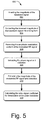
- FIG. 5 is a flow chart illustrating a process for linearization of a polar modulator using polar feedback receiver.
- This disclosure is directed towards techniques and methods of performing linearization in the polar modulator to attain linear amplification and high power efficiency during transmission.
- a polar modulator is described, it is contemplated that the techniques and methods may be applied to other modulators.
- the linearization may be implemented through the use of a polar feedback receiver in the polar demodulator to directly extract magnitude and phase baseband signal in modulated radio frequency (RF) output.
- RF radio frequency
- the polar feedback receiver avoids the use of additional circuitry (e.g., quadrature demodulator) which may include additional current consumption and delay sensitivity in the polar modulator.
- FIG. 1 illustrates a polar modulator component 100 that includes a baseband component 102 and a RF component 104 .
- baseband component 102 may encode a data signal; identify the data signal's prior state before modulation; convert the inphase signal (I) and quadrature phase signal (Q) into polar form; and transmit the data signal for modulation.
- Output from the baseband component 102 is referred to as a baseband signal.
- baseband component 102 may identify the prior state of the data signal following demodulation.
- the baseband component 102 decodes the demodulated data signal to re-create the data signal.
- the prior state of the data signal may include attributes of the data signal, such as amplitudes of I and Q, frequency, and phase amount.
- RF component 104 may combine the baseband signal with RF frequency carrier to produce a modulated RF frequency signal, amplify the modulated RF frequency signal, and further filter the modulated RF frequency signal before transmission.
- the RF frequency carrier may refer to the frequency of oscillation in the RF component 104 when a modulating baseband signal is not present.
- the RF component 104 may receive the modulated RF frequency signal, amplify the modulated RF frequency signal, filter the modulated RF frequency signal, and demodulate the modulated RF frequency signal.
- a signal from peripherals, camera, display etc. 106 may be received by Input/Output (I/O) component 108 for initial processing.
- the I/O component 108 may convert analog data signals into digital data signals, while the digital data signals are maintained in the same state (i.e., remain digital). Furthermore, the I/O component 108 may process the data signals to produce the amplitudes of I and Q.
- the data signals 110 are received by a digital signal processor (DSP) 112 .
- the DSP 112 may use a filter to limit the bandwidth forming a spectrum of the equivalent low pass signal or baseband signal.
- the DSP 112 may include a Coordinate Rotation Digital Computer (CORDIC) component to transform the amplitudes of I and Q of the baseband signal into equivalent polar representations.
- CORDIC Coordinate Rotation Digital Computer
- the equivalent polar representations may contain the phase and magnitude of the baseband signal, where the magnitude of the baseband signal may also refer to amplitude of the baseband signal.
- the baseband signal from the DSP 112 may pass through digital interface 114 .
- the digital interface 114 may provide concurrent bi-directional communications between the baseband component 102 and RF component 104 .
- the digital interface 114 may contain clock signals to provide timing references for transmit and receive communications between baseband component 102 and RF component 104 .
- phase modulator/analog signal processing component 116 During transmission, the baseband signal from digital interface 114 is received by phase modulator/analog signal processing component 116 .
- the phase modulator/analog signal processing component 116 may include an output that contains the modulated RF signal by varying the phase and magnitude of the RF carrier corresponding to the baseband signal to be transmitted.
- the phase modulator/analog signal processing component 116 may further support the linearization mechanism for the polar modulator 100 .
- a modulated RF signal 118 which is the output of phase modulator/analog signal processing component 116 , is passed to a nonlinear amplifier 120 for further amplification before transmission.
- the nonlinear amplifier 120 may include a relatively high power efficient amplifier suitable for varying envelope and phase modulation scheme.
- a modulated RF signal 122 is an output of the nonlinear amplifier 120 .
- the modulated signal 122 may contain distortions which may cause interference in the adjacent channels.
- the distortions may be caused by unexpected delay between the phase modulation signal and amplitude modulation signal.
- the unexpected delay may result in the signals (e.g., phase modulation and amplitude modulation) being applied to different portions of the RF carrier.
- the amplitude modulation may cause inadvertent phase modulation due to undesired feedback between phase modulation components and amplitude modulation components.
- the distortions may not only cause interference to the adjacent channels, but may also affect reception at the receiving end. Therefore, the distortions should be avoided in order to produce linear amplification, and for high power efficiency transmission.
- linearization may be used to compensate for the distortions at the polar modulator 100 .
- the linearization may include coupling of the polar modulator 100 output (i.e., signal 122 ) into a polar feedback receiver 124 .
- the polar feedback receiver 124 may be used for polar demodulation of the loop back polar modulator 100 output in order to directly extract the phase and magnitude of the modulated RF signal.
- a linearization mechanism that includes the polar feedback receiver 124 may be made adaptive by extracting an error signal (e.g., phase and magnitude distortion) coefficient at the output (i.e., signal 122 ) of the polar modulator 100 .
- the error signal coefficient may include unexpected delay between the phase modulation signal and amplitude modulation signal which may result in distortions in the polar modulator 100 .
- An input path signal 126 to the nonlinear amplifier 120 may be adjusted in accordance with the extracted error signal coefficient (e.g., phase and magnitude distortion) of the polar modulator 100 during real time operation, to effectively and continuously minimize distortion in the polar modulator 100 output.
- the adjusted modulated RF signal may be transmitted through antenna 128 .
- FIG. 2 illustrates a RF component 104 using the polar feedback receiver 124 for linearization of the polar modulator 100 .
- a baseband phase signal 200 and baseband magnitude signal 202 is received by RF component 104 .
- the phase signal component of the baseband signal may phase modulate the RF frequency carrier through the use of a local oscillator, phase detector, charge pump, filter, voltage controlled oscillator (VCO), and a multi modulus divider (MMD).
- the phase modulated RF signal may further undergo amplitude modulation by the baseband magnitude signal 202 to produce the varying envelope and phase modulation scheme.
- the modulated RF signal 122 is coupled from the output of the polar modulator 100 .
- the modulated RF signal (i.e., signal 122 ) may include the phase and magnitude of the baseband signal, together with the distortions, which may be demodulated by polar feedback receiver 124 .
- the polar feedback receiver 124 may implement polar demodulation of the coupled modulated RF signal by directly extracting the phase and magnitude baseband signal together with the distortions.
- the polar feedback receiver 124 may extract the phase and magnitude baseband signal and the distortions to be used for measuring the error signal coefficient at the output of the polar modulator 100 .
- the error signal coefficient may be used to compensate the phase and magnitude distortions to attain linear amplification and high power efficiency during transmission.
- the output of polar feedback receiver 124 may include the phase signal information plus distortion signal 204 and the magnitude signal information plus distortion signal 206 . Both signal 204 and signal 206 may enter algorithm component 208 which may be used to calculate error signal coefficient.
- the error signal coefficient may include the difference in gain between the phase and magnitude input sources, and the extracted phase and magnitude signal (including the distortions). The difference in gain may correspond to the calculated amount of distortion at the output of the polar modulator 100 which may be compensated to attain linear amplification and high power efficiency during transmission.
- the output 210 of the algorithm component 208 may include the magnitude error signal coefficient, and is received by Look Up Table (LUT) 212 for magnitude compensation.
- the output or signal 214 from algorithm 208 may include the phase error signal coefficient, and is received by LUT 216 for phase compensation.
- Both LUT 212 and LUT 216 may include a data structure used to replace a runtime computation with a simpler lookup operation.
- the LUT 212 may contain magnitude gain factors, corresponding to the magnitude error signal coefficient in signal 210 , which may be multiplied with the baseband magnitude signal 202 to produce the compensated magnitude signal.
- the LUT 216 may include phase gain factors, corresponding to the phase error signal coefficient in signal 214 , which may be multiplied with the baseband phase signal 200 to produce the compensated phase signal.
- a compensated magnitude signal 218 may be used for amplitude modulation in the polar modulator 100 .
- the compensated magnitude signal 218 may further be used as an input signal into the polar feedback receiver 124 in order to produce a limited modulated RF signal.
- the limited modulated RF signal may include the modulated RF signal whose amplitude modulation content is removed.
- the amplitude modulation content may be removed through combination of the modulated RF signal with a low frequency inverse baseband magnitude signal to produce the limited modulated RF signal.
- the amplitude modulation content removal may contain a low frequency local oscillator signal that may be used to split the modulated RF signal into phase modulation and amplitude modulation components.
- the local oscillator signal is the frequency signal that is normally used to split the modulated RF signal into phase modulation and amplitude modulation components in a quadrature demodulator.
- delay sensitivity may occur due to different processing circuitry of the modulated RF signal and the local oscillator signal which may be included in the quadrature demodulator.
- the low frequency inverse baseband magnitude may result from reversing the compensated magnitude signal 218 of the polar modulator 100 .
- the combined output of the modulated RF signal and the low frequency inverse baseband magnitude may include a limited modulated RF signal whose phase signal can be directly extracted through the use of a phase discriminator.
- the phase discriminator is a component where the phase signal information is extracted for a given limited modulated RF signal.
- the limited modulated RF signal may further be used to extract the magnitude of the modulated RF signal together with the distortion due to nonlinearities in the polar modulator 100 .
- the compensated magnitude signal 218 is received by a digital to analog converter (DAC) 220 for amplitude modulation of the polar modulator 100 .
- the DAC 220 may convert the compensated magnitude signal into analog compensated magnitude signal 222 received by mixer component 224 .
- the analog compensated magnitude signal 222 may be used to amplitude modulate the phase modulated signal in mixer component 224 .
- the mixer component 224 may combine the phase modulated RF signal with the analog compensated magnitude signal 222 in order to provide the varying envelope and phase modulation scheme for the polar modulator 100 .
- the compensated phase signal 226 may be used as a control signal for multi-modulus divider (MMD) 228 .
- MMD multi-modulus divider
- the MMD 228 may be used in the polar modulator 100 for low power, high operating frequencies, and high speed frequency synthesis applications to cover multiple frequency bands.
- the frequency synthesis applications may refer to a phase locked loop (PLL) based frequency synthesizer where the MMD 228 is placed between the output, and the feedback input includes the ability of the PLL to generate multiple frequencies at high speed applications.
- the MMD 228 may divide the output frequency of VCO 230 , where the output frequency is received by MMD 228 as signal 232 .
- the VCO 230 provides the up-converted frequency that is phase modulated by the baseband phase signal.
- Signal 234 is the output of MMD 228 received by phase detector (PD) 236 .
- the PD 236 provides a control signal which corresponds to the difference between the output of MMD 228 and signal 238 .
- the signal 238 may include a reference frequency generated by local oscillator 240 , which produces a constant reference frequency used for phase modulation in the polar modulator 100 .
- the output or signal 242 of the PD 236 is received by charge pump/filter 244 .
- the charge pump/filter 244 may include a positive output current and a negative output current activated by the control signal from PD 236 .
- the positive output current or negative output current may be filtered by a low pass filter to produce a DC voltage or control voltage signal 246 to sustain operation of the VCO 230 at a desired frequency.
- Signal 248 may include the phase modulated output of VCO 230 entering into mixer component 224 for amplitude modulation.
- the output of mixer component 228 which may contain the varying envelope and phase modulated RF signal may pass through signal 118 for amplification in the nonlinear amplifier 120 .
- FIG. 3 illustrates a polar feedback receiver 124 used for linearization of the polar modulator 100 .
- a compensated magnitude signal 218 is received by an inverse baseband magnitude component 300 .
- the inverse baseband magnitude component 300 may include a gain that reverses the compensated magnitude signal in signal 218 .
- the reversed baseband magnitude signal 302 may include a low frequency inverse baseband magnitude signal used to directly extract the phase and magnitude signals in the modulated RF signal.
- Signal 302 may include low frequency inverse baseband magnitude received by DAC 304 .
- the DAC 304 may convert the digital low frequency inverse baseband magnitude into analog low frequency inverse baseband magnitude to match the analog modulated RF output in signal 122 .
- the analog signal low frequency inverse baseband magnitude signal 306 is received by mixer component 308 for amplitude modulation content removal.
- the mixer component 308 may operate as a variable gain stage where one input signal may include the modulated RF signal 122 , and the other signal may include the analog low frequency inverse baseband magnitude signal 306 .
- the mixer component 308 operating as a variable gain stage, may strip away the amplitude modulation content without using additional circuitry like a local oscillator in quadrature demodulator. Removal of the amplitude modulation content in mixer component 308 may result in a limited modulated RF signal, and the phase information may be restored efficiently as compared to using a typical quadrature demodulator.
- Limited modulated RF signal 310 may include a constant envelope phase modulated signal.
- the limited modulated RF signal 310 may be used to directly extract the phase component plus distortion of the modulated RF signal 122 through the use of a phase discriminator 312 .
- the phase discriminator 312 may include amplitude variations in the output, which is a function of phase variation in the limited modulated RF signal 310 .
- the limited modulated RF signal 310 may also be used to extract the magnitude of the modulated RF signal 122 through mixer component 312 .
- the mixer component 312 may combine the magnitude of the modulated RF signal 122 , and the limited modulated RF signal 310 .
- the mixer component 312 may include an output that includes the magnitude of the baseband signal plus the distortion.
- FIG. 4 illustrates an implementation of a polar feedback receiver 124 , which includes direct extraction of distortions without the phase or magnitude component.
- the phase discriminator 312 may be implemented using a sigma delta converter, MMD component, and time to digital converter (TDC) component.
- An MMD 400 component divides the limited modulated RF signal 310 , and removes the phase modulation, without the phase distortion, through the use of a sigma to delta converter 402 .
- the sigma to delta converter 402 may include high precision conversion of the low frequency baseband phase signal 226 into an analog baseband phase signal 404 .
- the output signal 406 of MMD 400 may include the analog phase distortion output and is received by TDC 408 .
- the TDC 408 compares the signal edges of signal 406 to generate a delta time signal which can be converted to a delta time phase signal.
- the output signal 410 of TDC 408 may include only phase distortion.
- the mixer component 314 may operate in linear mode (i.e., acts as a multiplier), and the signal 412 may include the magnitude of the modulated RF signal 122 and the square of the distortion.
- An analog to digital converter (ADC) 414 converts the extracted magnitude signal together with the square of the distortion, into a digital signal 416 .
- the digital signal 416 is received by 1/M Square Root component 418 .
- the 1/M Square Root component 418 divides the signal 416 by the baseband magnitude signal and calculates the square root of the distortion signal to produce signal 420 which may only include the amount of magnitude distortion.
- FIG. 5 illustrates an exemplary method 500 for feedback receiver used for linearization in a modulator.
- the exemplary method 500 can be implemented in the polar modulator 100 .
- the exemplary method 500 is described with reference to FIGS. 1-4 .
- the order in which the method is described is not intended to be construed as a limitation, and any number of the described method blocks can be combined in any order to implement the method, or alternate method. Additionally, individual blocks may be deleted from the method without departing from the spirit and scope of the subject matter described herein.
- the method can be implemented in any suitable hardware, software, firmware, or a combination thereof, without departing from the scope of the invention.
- inverse baseband magnitude component 300 may include a gain that reverses the magnitude of the baseband signal to produce an inverse magnitude of the baseband signal in the polar modulator (e.g., polar modulator 100 ).
- converting the inverse magnitude of the baseband signal into analog form may convert the inverse magnitude of the baseband signal into analog inverse magnitude of the baseband signal.
- a mixer e.g., mixer component 308
- the mixer e.g., mixer component 308
- phase discriminator e.g., phase discriminator 312
- the limited modulated RF signal may be used as an input to a mixer (e.g., mixer component 314 ) which directly extracts the magnitude and distortion of the modulated RF signal by combining the modulated RF signal with the limited modulated RF signal.
- a mixer e.g., mixer component 314
- calculating an error signal coefficient for linearization of the polar modulator is performed.
- the algorithm e.g., algorithm 208
Landscapes
- Engineering & Computer Science (AREA)
- Computer Networks & Wireless Communication (AREA)
- Signal Processing (AREA)
- Power Engineering (AREA)
- Physics & Mathematics (AREA)
- Nonlinear Science (AREA)
- Amplifiers (AREA)
- Transmitters (AREA)
Abstract
Description
Claims (15)
Priority Applications (1)
| Application Number | Priority Date | Filing Date | Title |
|---|---|---|---|
| US13/923,720 US8626082B2 (en) | 2008-12-03 | 2013-06-21 | Polar feedback receiver for modulator |
Applications Claiming Priority (2)
| Application Number | Priority Date | Filing Date | Title |
|---|---|---|---|
| US12/327,687 US8666325B2 (en) | 2008-12-03 | 2008-12-03 | Polar feedback receiver for modulator |
| US13/923,720 US8626082B2 (en) | 2008-12-03 | 2013-06-21 | Polar feedback receiver for modulator |
Related Parent Applications (1)
| Application Number | Title | Priority Date | Filing Date |
|---|---|---|---|
| US12/327,687 Division US8666325B2 (en) | 2008-12-03 | 2008-12-03 | Polar feedback receiver for modulator |
Publications (2)
| Publication Number | Publication Date |
|---|---|
| US20130294543A1 US20130294543A1 (en) | 2013-11-07 |
| US8626082B2 true US8626082B2 (en) | 2014-01-07 |
Family
ID=42168966
Family Applications (2)
| Application Number | Title | Priority Date | Filing Date |
|---|---|---|---|
| US12/327,687 Expired - Fee Related US8666325B2 (en) | 2008-12-03 | 2008-12-03 | Polar feedback receiver for modulator |
| US13/923,720 Expired - Fee Related US8626082B2 (en) | 2008-12-03 | 2013-06-21 | Polar feedback receiver for modulator |
Family Applications Before (1)
| Application Number | Title | Priority Date | Filing Date |
|---|---|---|---|
| US12/327,687 Expired - Fee Related US8666325B2 (en) | 2008-12-03 | 2008-12-03 | Polar feedback receiver for modulator |
Country Status (2)
| Country | Link |
|---|---|
| US (2) | US8666325B2 (en) |
| DE (1) | DE102009056150B4 (en) |
Families Citing this family (23)
| Publication number | Priority date | Publication date | Assignee | Title |
|---|---|---|---|---|
| US8044742B2 (en) | 2009-03-11 | 2011-10-25 | Qualcomm Incorporated | Wideband phase modulator |
| US8588720B2 (en) * | 2009-12-15 | 2013-11-19 | Qualcomm Incorproated | Signal decimation techniques |
| WO2011074257A1 (en) * | 2009-12-15 | 2011-06-23 | パナソニック株式会社 | Wireless relaying device, wireless transmission device, and wireless relaying method |
| US8369807B2 (en) * | 2010-06-03 | 2013-02-05 | Broadcom Corporation | Polar-based RF receiver |
| US9000858B2 (en) | 2012-04-25 | 2015-04-07 | Qualcomm Incorporated | Ultra-wide band frequency modulator |
| US20150049793A1 (en) * | 2013-08-16 | 2015-02-19 | Qualcomm Incorporated | Interface sharing between digital and radio frequency circuits |
| US9203420B2 (en) | 2014-02-05 | 2015-12-01 | Innophase Inc. | Apparatus and method for digital to analog conversion with current mirror amplification |
| US9722642B2 (en) * | 2014-10-17 | 2017-08-01 | Texas Instruments Incorporated | Compensation parameter and predistortion signal |
| US9497055B2 (en) | 2015-02-27 | 2016-11-15 | Innophase Inc. | Method and apparatus for polar receiver with digital demodulation |
| US10158509B2 (en) | 2015-09-23 | 2018-12-18 | Innophase Inc. | Method and apparatus for polar receiver with phase-amplitude alignment |
| US9673829B1 (en) | 2015-12-02 | 2017-06-06 | Innophase, Inc. | Wideband polar receiver architecture and signal processing methods |
| US9673828B1 (en) | 2015-12-02 | 2017-06-06 | Innophase, Inc. | Wideband polar receiver architecture and signal processing methods |
| US10122397B2 (en) | 2017-03-28 | 2018-11-06 | Innophase, Inc. | Polar receiver system and method for Bluetooth communications |
| US10148230B2 (en) | 2017-03-28 | 2018-12-04 | Innophase, Inc. | Adaptive digital predistortion for polar transmitter |
| US10108148B1 (en) | 2017-04-14 | 2018-10-23 | Innophase Inc. | Time to digital converter with increased range and sensitivity |
| US10503122B2 (en) | 2017-04-14 | 2019-12-10 | Innophase, Inc. | Time to digital converter with increased range and sensitivity |
| US10622959B2 (en) | 2018-09-07 | 2020-04-14 | Innophase Inc. | Multi-stage LNA with reduced mutual coupling |
| US10840921B2 (en) | 2018-09-07 | 2020-11-17 | Innophase Inc. | Frequency control word linearization for an oscillator |
| US11095296B2 (en) | 2018-09-07 | 2021-08-17 | Innophase, Inc. | Phase modulator having fractional sample interval timing skew for frequency control input |
| US10728851B1 (en) | 2019-01-07 | 2020-07-28 | Innophase Inc. | System and method for low-power wireless beacon monitor |
| US10826738B2 (en) | 2019-01-07 | 2020-11-03 | Innophase Inc. | Systems and methods for maximizing power efficiency of a digital power amplifier in a polar transmitter |
| WO2020146408A1 (en) | 2019-01-07 | 2020-07-16 | Innophase, Inc. | Using a multi-tone signal to tune a multi-stage low-noise amplifier |
| US10651876B1 (en) | 2019-06-12 | 2020-05-12 | Innophase Inc. | System and method for dividing the carrier center frequency of an RF modulated signal by a non-integer divisor |
Citations (13)
| Publication number | Priority date | Publication date | Assignee | Title |
|---|---|---|---|---|
| US6194963B1 (en) | 1998-11-18 | 2001-02-27 | Ericsson Inc. | Circuit and method for I/Q modulation with independent, high efficiency amplitude modulation |
| US6266517B1 (en) * | 1999-12-30 | 2001-07-24 | Motorola, Inc. | Method and apparatus for correcting distortion in a transmitter |
| US20020101938A1 (en) | 2001-02-01 | 2002-08-01 | Masato Horaguchi | Predistortion type distortion compensation apparatus |
| US20020196864A1 (en) | 2001-06-19 | 2002-12-26 | Booth Richard W.D. | Hybrid polar modulator differential phase cartesian feedback correction circuit for power amplifier linearization |
| US6650875B1 (en) | 2000-08-30 | 2003-11-18 | Skyworks Solutions, Inc. | Transmitter architecture having a secondary phase-error correction loop including an amplitude reconstruction system |
| US6928272B2 (en) | 2001-12-04 | 2005-08-09 | Nec Corporation | Distortion compensating circuit for compensating distortion occurring in power amplifier |
| US20060160499A1 (en) | 2004-12-14 | 2006-07-20 | Puma Giuseppe L | Polar modulator and method for modulation of a signal |
| US20060189285A1 (en) | 2002-05-31 | 2006-08-24 | Ryoichi Takano | Communication semiconductor integrated circuit, a wireless communication apparatus, and a loop gain calibration method |
| US7215931B2 (en) * | 2001-06-19 | 2007-05-08 | Sirific Wireless Corporation | Method and apparatus for up-and-down-conversion of radio frequency (RF) signals |
| US7248643B2 (en) | 2002-06-05 | 2007-07-24 | Matsushita Electric Industrial Co., Ltd. | Distortion compensator |
| US7346122B1 (en) | 2002-08-21 | 2008-03-18 | Weixun Cao | Direct modulation of a power amplifier with adaptive digital predistortion |
| US7558542B2 (en) | 2006-06-09 | 2009-07-07 | Mediatek Inc. | System and method for providing a transmitter for polar modulation and power amplifier linearization |
| US20110050319A1 (en) * | 2007-09-03 | 2011-03-03 | Toumaz Technology Limited | Multiplier, Mixer, Modulator, Receiver and Transmitter |
Family Cites Families (1)
| Publication number | Priority date | Publication date | Assignee | Title |
|---|---|---|---|---|
| US6043707A (en) * | 1999-01-07 | 2000-03-28 | Motorola, Inc. | Method and apparatus for operating a radio-frequency power amplifier as a variable-class linear amplifier |
-
2008
- 2008-12-03 US US12/327,687 patent/US8666325B2/en not_active Expired - Fee Related
-
2009
- 2009-11-27 DE DE102009056150.1A patent/DE102009056150B4/en active Active
-
2013
- 2013-06-21 US US13/923,720 patent/US8626082B2/en not_active Expired - Fee Related
Patent Citations (13)
| Publication number | Priority date | Publication date | Assignee | Title |
|---|---|---|---|---|
| US6194963B1 (en) | 1998-11-18 | 2001-02-27 | Ericsson Inc. | Circuit and method for I/Q modulation with independent, high efficiency amplitude modulation |
| US6266517B1 (en) * | 1999-12-30 | 2001-07-24 | Motorola, Inc. | Method and apparatus for correcting distortion in a transmitter |
| US6650875B1 (en) | 2000-08-30 | 2003-11-18 | Skyworks Solutions, Inc. | Transmitter architecture having a secondary phase-error correction loop including an amplitude reconstruction system |
| US20020101938A1 (en) | 2001-02-01 | 2002-08-01 | Masato Horaguchi | Predistortion type distortion compensation apparatus |
| US7215931B2 (en) * | 2001-06-19 | 2007-05-08 | Sirific Wireless Corporation | Method and apparatus for up-and-down-conversion of radio frequency (RF) signals |
| US20020196864A1 (en) | 2001-06-19 | 2002-12-26 | Booth Richard W.D. | Hybrid polar modulator differential phase cartesian feedback correction circuit for power amplifier linearization |
| US6928272B2 (en) | 2001-12-04 | 2005-08-09 | Nec Corporation | Distortion compensating circuit for compensating distortion occurring in power amplifier |
| US20060189285A1 (en) | 2002-05-31 | 2006-08-24 | Ryoichi Takano | Communication semiconductor integrated circuit, a wireless communication apparatus, and a loop gain calibration method |
| US7248643B2 (en) | 2002-06-05 | 2007-07-24 | Matsushita Electric Industrial Co., Ltd. | Distortion compensator |
| US7346122B1 (en) | 2002-08-21 | 2008-03-18 | Weixun Cao | Direct modulation of a power amplifier with adaptive digital predistortion |
| US20060160499A1 (en) | 2004-12-14 | 2006-07-20 | Puma Giuseppe L | Polar modulator and method for modulation of a signal |
| US7558542B2 (en) | 2006-06-09 | 2009-07-07 | Mediatek Inc. | System and method for providing a transmitter for polar modulation and power amplifier linearization |
| US20110050319A1 (en) * | 2007-09-03 | 2011-03-03 | Toumaz Technology Limited | Multiplier, Mixer, Modulator, Receiver and Transmitter |
Non-Patent Citations (4)
| Title |
|---|
| Final Office Action dated Jan. 30, 2012 for U.S. Appl. No. 12/327,687. |
| Office Action dated Aug. 22, 2012 for U.S. Appl. No. 12/327,687. |
| Office Action dated Jul. 14, 2011 for U.S. Appl. No. 12/327,687. |
| Office Action dated Nov. 16, 2012 for U.S. Appl. No. 12/327,687. |
Also Published As
| Publication number | Publication date |
|---|---|
| DE102009056150A1 (en) | 2010-06-17 |
| US20130294543A1 (en) | 2013-11-07 |
| US8666325B2 (en) | 2014-03-04 |
| DE102009056150B4 (en) | 2017-09-14 |
| US20100136937A1 (en) | 2010-06-03 |
Similar Documents
| Publication | Publication Date | Title |
|---|---|---|
| US8626082B2 (en) | Polar feedback receiver for modulator | |
| US8565338B2 (en) | High bandwidth modulation and transmission | |
| US7817970B2 (en) | Transmitting/receiving device having a polar modulator with variable predistortion | |
| US7346122B1 (en) | Direct modulation of a power amplifier with adaptive digital predistortion | |
| US6928122B2 (en) | Amplifier predistortion system and method | |
| US6993091B2 (en) | Correction of DC-offset of I/Q modulator | |
| JP2000286915A (en) | Signal modulation circuit and method | |
| US9699014B2 (en) | Digital modulation jitter compensation for polar transmitter | |
| JPH08163189A (en) | Transmission circuit | |
| WO2006118056A1 (en) | Two-point modulation type phase modulating apparatus, polar modulation transmitting apparatus, radio transmitting apparatus, and wireless communication apparatus | |
| US6844787B2 (en) | Method and apparatus for re-modulation using zero IF | |
| US12057813B2 (en) | Wideband transmission circuit | |
| JP2009171460A (en) | Communication device, oscillator and frequency synthesizer | |
| JP4584336B2 (en) | Polar modulation apparatus and method using FM modulation | |
| US6963620B2 (en) | Communication transmitter using offset phase-locked-loop | |
| US8648655B2 (en) | Modulator and an amplifier using the same | |
| US8532590B2 (en) | Digital phase feedback for determining phase distortion | |
| JP4214635B2 (en) | Digital radio equipment | |
| JP4128488B2 (en) | Transmission circuit device and wireless communication device | |
| JPWO2015114702A1 (en) | Transmitting apparatus and control method thereof | |
| JP3990401B2 (en) | Transmitter | |
| US20050143025A1 (en) | Transmitting apparatus | |
| Xu et al. | Analog carrier recovery circuits for six‐port direct digital receivers |
Legal Events
| Date | Code | Title | Description |
|---|---|---|---|
| STCF | Information on status: patent grant |
Free format text: PATENTED CASE |
|
| AS | Assignment |
Owner name: INTEL DEUTSCHLAND GMBH, GERMANY Free format text: CHANGE OF NAME;ASSIGNOR:INTEL MOBILE COMMUNICATIONS GMBH;REEL/FRAME:037057/0061 Effective date: 20150507 |
|
| FEPP | Fee payment procedure |
Free format text: MAINTENANCE FEE REMINDER MAILED (ORIGINAL EVENT CODE: REM.) |
|
| FEPP | Fee payment procedure |
Free format text: SURCHARGE FOR LATE PAYMENT, LARGE ENTITY (ORIGINAL EVENT CODE: M1554) |
|
| MAFP | Maintenance fee payment |
Free format text: PAYMENT OF MAINTENANCE FEE, 4TH YEAR, LARGE ENTITY (ORIGINAL EVENT CODE: M1551) Year of fee payment: 4 |
|
| FEPP | Fee payment procedure |
Free format text: MAINTENANCE FEE REMINDER MAILED (ORIGINAL EVENT CODE: REM.); ENTITY STATUS OF PATENT OWNER: LARGE ENTITY |
|
| LAPS | Lapse for failure to pay maintenance fees |
Free format text: PATENT EXPIRED FOR FAILURE TO PAY MAINTENANCE FEES (ORIGINAL EVENT CODE: EXP.); ENTITY STATUS OF PATENT OWNER: LARGE ENTITY |
|
| STCH | Information on status: patent discontinuation |
Free format text: PATENT EXPIRED DUE TO NONPAYMENT OF MAINTENANCE FEES UNDER 37 CFR 1.362 |
|
| FP | Lapsed due to failure to pay maintenance fee |
Effective date: 20220107 |
|
| AS | Assignment |
Owner name: INTEL CORPORATION, CALIFORNIA Free format text: ASSIGNMENT OF ASSIGNORS INTEREST;ASSIGNOR:INTEL DEUTSCHLAND GMBH;REEL/FRAME:061356/0001 Effective date: 20220708 |