US8552799B2 - Power amplifying circuit - Google Patents
Power amplifying circuit Download PDFInfo
- Publication number
- US8552799B2 US8552799B2 US13/418,594 US201213418594A US8552799B2 US 8552799 B2 US8552799 B2 US 8552799B2 US 201213418594 A US201213418594 A US 201213418594A US 8552799 B2 US8552799 B2 US 8552799B2
- Authority
- US
- United States
- Prior art keywords
- operational amplifier
- feedback resistor
- input terminal
- inverting input
- output terminal
- Prior art date
- Legal status (The legal status is an assumption and is not a legal conclusion. Google has not performed a legal analysis and makes no representation as to the accuracy of the status listed.)
- Active, expires
Links
- 239000003990 capacitor Substances 0.000 claims description 5
- 238000010586 diagram Methods 0.000 description 10
- ATJFFYVFTNAWJD-UHFFFAOYSA-N Tin Chemical group [Sn] ATJFFYVFTNAWJD-UHFFFAOYSA-N 0.000 description 8
- 230000000052 comparative effect Effects 0.000 description 6
- 238000000034 method Methods 0.000 description 2
- 238000012986 modification Methods 0.000 description 1
- 230000004048 modification Effects 0.000 description 1
- 238000006467 substitution reaction Methods 0.000 description 1
Images


Classifications
-
- H—ELECTRICITY
- H03—ELECTRONIC CIRCUITRY
- H03F—AMPLIFIERS
- H03F3/00—Amplifiers with only discharge tubes or only semiconductor devices as amplifying elements
- H03F3/68—Combinations of amplifiers, e.g. multi-channel amplifiers for stereophonics
-
- H—ELECTRICITY
- H03—ELECTRONIC CIRCUITRY
- H03F—AMPLIFIERS
- H03F1/00—Details of amplifiers with only discharge tubes, only semiconductor devices or only unspecified devices as amplifying elements
- H03F1/02—Modifications of amplifiers to raise the efficiency, e.g. gliding Class A stages, use of an auxiliary oscillation
- H03F1/0205—Modifications of amplifiers to raise the efficiency, e.g. gliding Class A stages, use of an auxiliary oscillation in transistor amplifiers
- H03F1/0211—Modifications of amplifiers to raise the efficiency, e.g. gliding Class A stages, use of an auxiliary oscillation in transistor amplifiers with control of the supply voltage or current
- H03F1/0244—Stepped control
-
- H—ELECTRICITY
- H03—ELECTRONIC CIRCUITRY
- H03F—AMPLIFIERS
- H03F1/00—Details of amplifiers with only discharge tubes, only semiconductor devices or only unspecified devices as amplifying elements
- H03F1/02—Modifications of amplifiers to raise the efficiency, e.g. gliding Class A stages, use of an auxiliary oscillation
- H03F1/0205—Modifications of amplifiers to raise the efficiency, e.g. gliding Class A stages, use of an auxiliary oscillation in transistor amplifiers
- H03F1/0277—Selecting one or more amplifiers from a plurality of amplifiers
-
- H—ELECTRICITY
- H03—ELECTRONIC CIRCUITRY
- H03F—AMPLIFIERS
- H03F3/00—Amplifiers with only discharge tubes or only semiconductor devices as amplifying elements
- H03F3/181—Low-frequency amplifiers, e.g. audio preamplifiers
- H03F3/183—Low-frequency amplifiers, e.g. audio preamplifiers with semiconductor devices only
- H03F3/187—Low-frequency amplifiers, e.g. audio preamplifiers with semiconductor devices only in integrated circuits
-
- H—ELECTRICITY
- H03—ELECTRONIC CIRCUITRY
- H03F—AMPLIFIERS
- H03F3/00—Amplifiers with only discharge tubes or only semiconductor devices as amplifying elements
- H03F3/45—Differential amplifiers
- H03F3/45071—Differential amplifiers with semiconductor devices only
- H03F3/45076—Differential amplifiers with semiconductor devices only characterised by the way of implementation of the active amplifying circuit in the differential amplifier
- H03F3/45475—Differential amplifiers with semiconductor devices only characterised by the way of implementation of the active amplifying circuit in the differential amplifier using IC blocks as the active amplifying circuit
-
- H—ELECTRICITY
- H03—ELECTRONIC CIRCUITRY
- H03F—AMPLIFIERS
- H03F2203/00—Indexing scheme relating to amplifiers with only discharge tubes or only semiconductor devices as amplifying elements covered by H03F3/00
- H03F2203/45—Indexing scheme relating to differential amplifiers
- H03F2203/45138—Two or more differential amplifiers in IC-block form are combined, e.g. measuring amplifiers
Definitions
- Embodiments described herein relate generally to a power amplifying circuit.
- the idling stop and start function is to prevent the audio output from the car audio system from being interrupted by an instantaneous drop of the battery voltage caused by an abrupt load change when the engine is restarted.
- the idling stop and start function allows a user to comfortably listen to the audio output from the car audio system even when the engine is restarted.
- FIG. 1 is a diagram showing a configuration of a power amplifying circuit 100 X according to a comparative example that is not adapted for idling stop;
- FIG. 2 is a diagram showing a waveform of an operation of the power amplifying circuit 100 X according to the comparative example shown in FIG. 1 ;
- FIG. 3 is a diagram showing an example of a configuration of a power amplifying circuit 100 according to a first embodiment
- FIG. 4 is a diagram showing an example of a specific circuit configuration of the midpoint potential controlling circuit 1 shown in FIG. 3 ;
- FIG. 5 is a diagram showing an example of a specific waveform of an operation of the power amplifying circuit 100 according to the first embodiment shown in FIG. 3 .
- a power amplifying circuit includes a first operational amplifier connected to a first signal input terminal at a non-inverting input terminal thereof.
- the power amplifying circuit includes a first feedback resistor connected between an output terminal of the first operational amplifier and an inverting input terminal of the first operational amplifier.
- the power amplifying circuit includes a second feedback resistor connected to the inverting input terminal of the first operational amplifier at a first end thereof.
- the power amplifying circuit includes a second operational amplifier connected to a second signal input terminal at a non-inverting input terminal thereof.
- the power amplifying circuit includes a third feedback resistor connected to an inverting input terminal of the second operational amplifier at a first end thereof and to a second end of the second feedback resistor at a second end thereof.
- the power amplifying circuit includes a fourth feedback resistor connected between an output terminal of the second operational amplifier and an inverting input terminal of the second operational amplifier.
- the power amplifying circuit includes a fully differential operational amplifier that is connected to the output terminal of the first operational amplifier at a non-inverting input terminal thereof, to the output terminal of the second operational amplifier at an inverting input terminal thereof, to a first signal output terminal at a non-inverting output terminal thereof, and to a second signal output terminal at an inverting output terminal thereof and maintains a constant differential gain.
- the power amplifying circuit includes a switching circuit connected between the second end of the second feedback resistor and the ground.
- the power amplifying circuit includes a first input resistor connected between the first signal input terminal and a reference terminal to which a reference voltage is applied.
- the power amplifying circuit includes a second input resistor connected between the second signal input terminal and the reference terminal.
- the power amplifying circuit includes a midpoint potential controlling circuit that monitors a power supply voltage and controls the switching circuit based on the value of the power supply voltage.
- the midpoint potential controlling circuit turns on the switching circuit when the power supply voltage is equal to or higher than a preset switching threshold.
- the midpoint potential controlling circuit turns off the switching circuit when the power supply voltage is lower than the switching threshold.
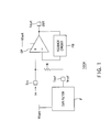
- FIG. 1 is a diagram showing a configuration of a power amplifying circuit 100 X according to a comparative example that is not adapted for idling stop.
- FIG. 2 is a diagram showing a waveform of an operation of the power amplifying circuit 100 X according to the comparative example shown in FIG. 1 .
- the power amplifying circuit 100 X includes an operational amplifier OP, a feedback circuit “FB”, and a resistor R.
- a reference voltage “Vref” is supplied through a supply voltage rejection (SVR) filter F to a reference terminal (SVR terminal) “Tref” of the power amplifying circuit 100 X.
- SVR supply voltage rejection
- the potential at an output terminal Tout of the power amplifying circuit 100 X is approximately equal to the reference voltage “Vref” at the reference terminal Tref and is set at an intermediate voltage of a power supply voltage (battery voltage) “Vbat”.
- the power amplifying circuit 100 X cannot keep a desired output waveform.
- the car audio system that incorporates the power amplifying circuit 100 X according to the comparative example that is not adapted for idling stop interrupts the audio output and makes the user feel discomfort when the engine is restarted and the battery voltage instantaneously drops because of the abrupt load change.
- FIG. 3 is a diagram showing an example of a configuration of a power amplifying circuit 100 according to a first embodiment.
- the power amplifying circuit 100 includes a midpoint potential controlling circuit 1 , a fully differential operational amplifier 3 , a first feedback resistor R 1 , a second feedback resistor R 2 , a third feedback resistor R 3 , a fourth feedback resistor R 4 , a first input resistor R 11 , a second input resistor R 12 , a first operational amplifier OP 1 , a second operational amplifier OP 2 , and a switching circuit SW.
- the first operational amplifier OP 1 is connected to a first signal input terminal Tin 1 at a non-inverting input terminal thereof.
- the first feedback resistor R 1 is connected between an output terminal of the first operational amplifier OP 1 and an inverting input terminal of the first operational amplifier OP 1 .
- the second feedback resistor R 2 is connected to the inverting input terminal of the first operational amplifier OP 1 at one end thereof.
- the second operational amplifier OP 2 is connected to a second signal input terminal Tin 2 at a non-inverting input terminal thereof.
- the third feedback resistor R 3 is connected to an inverting input terminal of the second operational amplifier OP 2 at one end thereof and to the other end of the second feedback resistor R 2 at the other end thereof.
- the fourth feedback resistor R 4 is connected between an output terminal of the second operational amplifier OP 2 and the inverting input terminal of the second operational amplifier OP 2 .
- the first to fourth feedback resistors R 1 to R 4 have a same first resistance Ra, for example.
- the fully differential operational amplifier 3 is connected to the output terminal of the first operational amplifier OP 1 at a non-inverting input terminal thereof, to the output terminal of the second operational amplifier OP 2 at an inverting input terminal thereof, to a first signal output terminal Tout 1 at a non-inverting output terminal thereof, and to a second signal output terminal at an inverting output terminal thereof.
- the fully differential operational amplifier 3 is configured to maintain a constant differential gain.
- the fully differential operational amplifier 3 includes a fifth feedback resistor R 5 , a sixth feedback resistor R 6 , a seventh feedback resistor R 7 , an eighth feedback resistor R 8 , a ninth feedback resistor R 9 , a tenth feedback resistor R 10 , a third operational amplifier OP 3 , and a fourth operational amplifier OP 4 , for example.
- the fifth feedback resistor “R 5 ” is connected to the non-inverting input terminal of the fully differential operational amplifier 3 (the output terminal of the first operational amplifier OP 1 ) at one end thereof.
- the sixth feedback resistor R 6 is connected to the inverting input terminal of the fully differential operational amplifier 3 (the output terminal of the second operational amplifier OP 2 ) at one end thereof.
- the seventh feedback resistor R 7 is connected to the other end of the fifth feedback resistor R 5 at one end thereof.
- the eighth feedback resistor R 8 is connected to the other end of the sixth feedback resistor R 6 at one end thereof.
- the third operational amplifier OP 3 is connected to the other end of the fifth feedback resistor R 5 at a non-inverting input terminal thereof, to the other end of the eighth feedback resistor R 8 at an inverting input terminal thereof, and to the non-inverting output terminal of the fully differential operational amplifier 3 (the first signal output terminal Tout 1 ) at an output terminal thereof.
- the ninth feedback resistor R 9 is connected between the output terminal of the third operational amplifier OP 3 and the inverting input terminal of the third operational amplifier OP 3 .
- the fourth operational amplifier OP 4 is connected to the other end of the sixth feedback resistor R 6 at a non-inverting input terminal thereof, to the other end of the seventh feedback resistor R 7 at an inverting input terminal thereof, and to the inverting output terminal of the fully differential operational amplifier 3 (the second signal output terminal Tout 2 ) at an output terminal thereof.
- the tenth feedback resistor R 10 is connected between the output terminal of the fourth operational amplifier OP 4 and the inverting input terminal of the fourth operational amplifier OP 4 .
- the fifth and sixth feedback resistors R 5 and R 6 have a same second resistance “Rb”, for example.
- the ninth and tenth feedback resistors R 9 and R 10 have a same third resistance “Rc”, for example.
- the resistances of the seventh and eighth feedback resistors R 7 and R 8 are negligibly small compared with the third resistance “Rc”, for example.
- the switching circuit SW is connected between the other end of the second feedback resistor R 2 and the ground.
- the first input resistor R 11 is connected between the first signal input terminal Tin 1 and the reference terminal (SVR terminal) Tref to which the reference voltage “Vref” is applied.
- the second input resistor R 12 is connected between the second signal input terminal Tin 2 and the reference terminal Tref.
- the reference voltage “Vref” is supplied to the reference terminal Tref from an SVR filter 2 .
- the SVR filter 2 generates the reference voltage “Vref” by dividing the power supply voltage “Vbat” into values lower than the intermediate voltage of the power supply voltage “Vbat” and raises the supply voltage rejection ratio with respect to the generated reference voltage “Vref” with a capacitor (not shown) connected between the reference terminal Tref and the ground.
- the reference voltage “Vref” is steady even if the power supply voltage “Vbat” varies due to idling stop or the like.
- the reference voltage “Vref” is set to be a quarter of the power supply voltage “Vbat”, for example.
- the midpoint potential controlling circuit 1 is configured to monitor the reference voltage “Vref” and the power supply voltage (battery voltage) “Vbat” and control the switching circuit SW according to the value of the power supply voltage “Vbat”.
- the midpoint potential controlling circuit 1 turns on the switching circuit SW if the power supply voltage “Vbat” is equal to or higher than a preset switching threshold “Vth” (if the power supply voltage “Vbat” is in a steady state), and turns off the switching circuit SW if the power supply voltage “Vbat” is lower than the switching threshold “Vth” (if the power supply voltage “Vbat” instantaneously drops).
- the switching threshold “Vth” for the power supply voltage “Vbat” is set at a value with which the first and second operational amplifiers OP 1 and OP 2 can operate to output a predetermined signal.
- the switching threshold “Vth” is set based on the reference voltage “Vref”.
- the switching threshold “Vth” is set to be higher than a half of the power supply voltage “Vbat” in the steady state.
- the midpoint potential controlling circuit 1 controls the switching circuit SW based on the result of comparison between the power supply voltage “Vbat” and the reference voltage “Vref”.
- FIG. 4 is a diagram showing an example of a specific circuit configuration of the midpoint potential controlling circuit 1 shown in FIG. 3 .
- the midpoint potential controlling circuit 1 includes resistors 1 a , 1 b , 1 e , 1 h , 1 j and 1 k , PNP-type bipolar transistors 1 c and 1 i , NPN-type bipolar transistors 1 d and 1 g , a constant current source 1 f , a Zener diode 1 l , an nMOS transistor 1 m , an output terminal 1 n , and a level shift circuit 1 o.
- the resistor 1 a is connected to the power supply (battery) at one end thereof.
- the resistor 1 b is connected between the other end of the resistor 1 a and the ground.
- the PNP-type bipolar transistor 1 c is connected to the power supply at the emitter thereof and is diode-connected.
- the NPN-type bipolar transistor 1 d is connected to the collector of the PNP-type bipolar transistor 1 c at the collector thereof and to the other end of the resistor 1 a at the base thereof.
- the resistor 1 e is connected to the emitter of the NPN-type bipolar transistor at one end thereof.
- the constant current source 1 f is connected between the other end of the resistor 1 e and the ground.
- the level shift circuit 1 o is configured to output a voltage level-shifted from the reference voltage “Vref” input to the reference terminal Tref.
- the NPN-type bipolar transistor 1 g is connected to the power supply at the collector thereof and to the output of the level shift circuit 1 o at the base thereof.
- the resistor 1 h is connected between the emitter of the NPN-type bipolar transistor 1 g and one end of the constant current source 1 f.
- the PNP-type bipolar transistor 1 i is connected to the power supply at the emitter thereof and to the base of the PNP-type bipolar transistor 1 c at the base thereof.
- the PNP-type bipolar transistor 1 i and the PNP-type bipolar transistor 1 c form a current mirror circuit.
- the resistor 1 j is connected to the collector of the PNP-type bipolar transistor 1 i at one end thereof.
- the resistor 1 k is connected between the other end of the resistor 1 j and the ground.
- the nMOS transistor 1 m is connected between the output terminal 1 n and the ground and connected to the other end of the resistor 1 j at the gate thereof.
- the Zener diode 1 l is connected to the gate of the nMOS transistor 1 m at the cathode thereof and to the source of the nMOS transistor 1 m at the anode thereof.
- the midpoint potential controlling circuit 1 configured as described above compares a voltage resulting from division of the power supply voltage “Vbat” by the resistors 1 a and 1 b with the voltage level-shifted from the reference voltage “Vref” by the level shift circuit 1 o and outputs a control signal Sc responsive to the result of the comparison from the output terminal 1 n.
- the midpoint potential controlling circuit 1 indirectly compares the power supply voltage “Vbat” with the switching threshold “Vth” based on the reference voltage “Vref” by the operation described above, and outputs the control signal Sc based on the result of the comparison.
- the power supply voltage “Vbat” is the battery voltage.
- the reference terminal Tref is a terminal at which a voltage lower than the intermediate voltage of the power supply voltage “Vbat”, for example, a quarter of the power supply voltage “Vbat”, is generated, and the supply voltage rejection ratio is raised by an external capacitor.
- the input signal is applied to the first signal input terminal Tin 1 , and the second signal input terminal Tin 2 is a virtually grounded point.
- a gain “K 1 ” of the first operational amplifier OP 1 is 2 as shown by the following formula (1).
- a gain K 2 of the second operational amplifier OP 2 can be determined in the same way.
- a differential gain “KA” of the differential output of the first operational amplifier OP 1 and the second operational amplifier OP 2 is also 2 as shown by the following formula (2) because the output of the second operational amplifier OP 2 is an alternating-current ground point since the second signal input terminal Tin 2 is a virtually grounded point.
- the first operational amplifier OP 1 and the second operational amplifier OP 2 are multiply-by-two DC amplifiers, and the reference voltage “Vref” at the reference terminal Tref is set to be a quarter of the power supply voltage “Vbat” in the steady state. Therefore, the output potentials of the first operational amplifier OP 1 and the second operational amplifier OP 2 are a half of the power supply voltage “Vbat”, that is, the intermediate potential of the power supply voltage “Vbat”.
- the differential gain of the fully differential operational amplifier 3 that is, the differential gain from the outputs of the first operational amplifier OP 1 and the second operational amplifier OP 2 to the first signal output terminal Tout 1 and the second signal output terminal Tout 2 , is denoted by “KB”. Since the resistances of the seventh and eighth feedback resistors are negligibly small compared with the resistances of the ninth and tenth feedback resistors as described above, the differential gain “KB” is approximately equal to Rc/Rb.
- the output potentials at the first signal output terminal Tout 1 and the second signal output terminal Tout 2 are close to the output potentials of the first operational amplifier OP 1 and the second operational amplifier OP 2 because of the action of the seventh and eighth feedback resistors R 7 and R 8 . If there were not the resistors R 7 and R 8 , the DC gains of the first operational amplifier OP 1 and the second operational amplifier OP 2 would be substantially infinite, and the output potentials at the terminals Tout 1 and Tout 2 would not be fixed at a desired voltage.
- the output potentials at the first signal output terminal Tout 1 and the second signal output terminal Tout 2 are approximately the intermediate potential of the power supply voltage “Vbat”.
- the differential gain “KA” of the outputs of the first operational amplifier OP 1 and the second operational amplifier OP 2 is 2 as shown by the following formula (5).
- the output potentials of the first operational amplifier OP 1 and the second operational amplifier OP 2 are approximately equal to the potential at the reference terminal Tref and are a quarter of the power supply voltage “Vbat”.
- the output potentials at the first signal output terminal Tout 1 and the second signal output terminal Tout 2 are close to the output potentials of the first operational amplifier OP 1 and the second operational amplifier OP 2 because of the action of the seventh and eighth feedback resistors R 7 and R 8 . Therefore, the output potentials at the first signal output terminal Tout 1 and the second signal output terminal Tout 2 are approximately a quarter of the power supply voltage “Vbat”.
- the differential gain “KB” of the fully differential operational amplifier 3 is approximately equal to Rc/Rb.
- the differential gain “K” of the power amplifying circuit 100 is always fixed at 2Rc/Rb regardless of whether the switching circuit SW is in the on state or off state. Depending on whether the switching circuit SW is in the on state or off state, only the direct-current output potentials at the first signal output terminal Tout 1 and the second signal output terminal Tout 2 change to the intermediate voltage of the power supply voltage “Vbat” or a quarter of the power supply voltage “Vbat”.
- FIG. 5 is a diagram showing an example of a specific waveform of an operation of the power amplifying circuit 100 according to the first embodiment shown in FIG. 3 .
- the switching threshold “Vth” is set as shown by the following formula (6).
- Vref denotes the reference voltage
- Vhr denotes a fixed voltage.
- Vth 2 Vref+Vhr (6)
- the waveform of the power supply voltage “Vbat” shows a typical instantaneous drop of the battery voltage that occurs when the engine is restarted after the idling stop state (from a time “t 1 ” to a time “t 4 ”).
- the power supply voltage (battery voltage) “Vbat” is in the steady state before the time “t 1 ” and after the time “t 4 ”.
- a direct-current output voltage “VoutDC” is the potential at the first signal output terminal Tout 1 and the second signal output terminal Tout 2 .
- the midpoint potential controlling circuit 1 turns on the switching circuit SW, thereby changing the direct-current output voltage “VoutDC” to a half of the power supply voltage “Vbat”.
- the midpoint potential controlling circuit 1 turns off the switching circuit SW, thereby changing the direct-current output voltage “VoutDC” to a quarter of the power supply voltage “Vbat”.
- a positive-phase output signal and a negative-phase output signal are output.
- clipping may occur at one of the output terminals (as shown by the arrow A in FIG. 5 ).
- the power amplifying circuit 100 maintains a constant differential gain, the differential output at the first signal output terminal Tout 1 and the second signal output terminal Tout 2 always exhibits a desired output waveform even before or after the instantaneous drop of the battery voltage (as shown by the arrow B in FIG. 5 ).
- the power amplifying circuit according to the first embodiment can keep a desired output waveform even when an instantaneous drop of the power supply voltage occurs.
- the car audio system incorporating the power amplifying circuit according to the first embodiment can prevent the audio output from interrupting when the engine is restarted after the idling stop state and the battery voltage instantaneously drops because of an abrupt load change. That is, the user can comfortably listen to the audio output from the car audio system even when the engine is restarted.
Landscapes
- Engineering & Computer Science (AREA)
- Power Engineering (AREA)
- Microelectronics & Electronic Packaging (AREA)
- Multimedia (AREA)
- Amplifiers (AREA)
Abstract
Description
K1=1+R1/R2=1+Ra/Ra=2 (1)
KA=K1−K2=2−0=2 (2)
K1=1+R1/(R2+R3)=1+Ra/(2Ra)=1.5 (3)
K2=−R4/(R2+R3)=−Ra/2Ra=−0.5 (4)
KA=K1−K2=1.5−(−0.5)=2 (5)
Vth=2Vref+Vhr (6)
Claims (20)
Applications Claiming Priority (2)
| Application Number | Priority Date | Filing Date | Title |
|---|---|---|---|
| JP2011176970A JP5498998B2 (en) | 2011-08-12 | 2011-08-12 | Power amplifier circuit |
| JP2011-176970 | 2011-08-12 |
Publications (2)
| Publication Number | Publication Date |
|---|---|
| US20130038395A1 US20130038395A1 (en) | 2013-02-14 |
| US8552799B2 true US8552799B2 (en) | 2013-10-08 |
Family
ID=47646659
Family Applications (1)
| Application Number | Title | Priority Date | Filing Date |
|---|---|---|---|
| US13/418,594 Active 2032-04-28 US8552799B2 (en) | 2011-08-12 | 2012-03-13 | Power amplifying circuit |
Country Status (3)
| Country | Link |
|---|---|
| US (1) | US8552799B2 (en) |
| JP (1) | JP5498998B2 (en) |
| CN (1) | CN102931929B (en) |
Cited By (3)
| Publication number | Priority date | Publication date | Assignee | Title |
|---|---|---|---|---|
| US20140176240A1 (en) * | 2012-10-24 | 2014-06-26 | Ipgoal Microelectronics (Sichuan) Co., Ltd. | High-frequency bandwidth amplifying circuit |
| US9602070B2 (en) | 2015-03-16 | 2017-03-21 | Kabushiki Kaisha Toshiba | Power amplifying device |
| US11171617B2 (en) | 2018-11-21 | 2021-11-09 | Kabushiki Kaisha Toshiba | Power amplifying device and audio equipment |
Families Citing this family (7)
| Publication number | Priority date | Publication date | Assignee | Title |
|---|---|---|---|---|
| JP6970644B2 (en) * | 2018-06-11 | 2021-11-24 | 日立Astemo株式会社 | Semiconductor devices and sensor systems |
| CN109995343B (en) * | 2019-03-27 | 2023-06-30 | 无锡海斯凯尔医学技术有限公司 | Impedance matching device and ultrasonic imaging system |
| US11190154B2 (en) * | 2019-06-14 | 2021-11-30 | Murata Manufacturing Co., Ltd. | Power amplifier circuit |
| CN113720962B (en) * | 2020-05-25 | 2025-02-07 | 深圳市特安电子有限公司 | A dual-range gas detection device and a gas detector |
| JP7657687B2 (en) * | 2021-09-22 | 2025-04-07 | 株式会社東芝 | Power Amplifier |
| CN116008646B (en) * | 2023-02-24 | 2025-12-05 | 北京鸿智电通科技有限公司 | Current detection circuit, current detection equipment and fast charging device |
| CN116760379B (en) * | 2023-08-21 | 2024-12-27 | 长春精意科技有限公司 | Signal power control circuit of communication system equipment |
Citations (8)
| Publication number | Priority date | Publication date | Assignee | Title |
|---|---|---|---|---|
| JPH03283804A (en) | 1990-03-30 | 1991-12-13 | Hitachi Ltd | Audio amplifier |
| US6107886A (en) | 1998-03-31 | 2000-08-22 | Kabushiki Kaisha Toshiba | High-efficiency power amplifier |
| JP3283804B2 (en) | 1996-10-07 | 2002-05-20 | ビステオン・テクノロジーズ,エル・エル・シー | Method and apparatus for selecting a destination in a vehicle navigation system |
| US7227409B2 (en) * | 2004-11-25 | 2007-06-05 | Sunplus Technology Co., Ltd. | Apparatus for removing DC offset and amplifying signal with variable gain simultaneously |
| US7230482B2 (en) * | 2003-12-23 | 2007-06-12 | Stmicroelectronics S.R.L. | Method of preventing abrupt voltage changes at the outputs of a pair of amplifiers and control circuit for a pair of amplifiers self-configuring in a bridge configuration |
| US7420413B2 (en) | 2005-08-05 | 2008-09-02 | Kabushiki Kaisha Toshiba | Amplifier circuit of BTL system |
| US7525375B2 (en) * | 2005-12-20 | 2009-04-28 | Mettler-Toledo Ag | Method of correcting the output signal of an analog amplifier, amplifier module and measuring device |
| US20110193631A1 (en) | 2010-02-05 | 2011-08-11 | Kabushiki Kaisha Toshiba | Amplifier |
Family Cites Families (9)
| Publication number | Priority date | Publication date | Assignee | Title |
|---|---|---|---|---|
| US4337441A (en) * | 1980-02-11 | 1982-06-29 | Tektronix, Inc. | Supply-voltage driver for a differential amplifier |
| JPH0112411Y2 (en) * | 1980-09-22 | 1989-04-11 | ||
| JPH0736499B2 (en) * | 1989-10-06 | 1995-04-19 | 日本電気アイシーマイコンシステム株式会社 | Power amplifier circuit |
| JP2665072B2 (en) * | 1991-05-21 | 1997-10-22 | 日本電気アイシーマイコンシステム株式会社 | Amplifier circuit |
| JP3260098B2 (en) * | 1997-06-03 | 2002-02-25 | 松下電器産業株式会社 | BTL amplifier |
| JP3071700U (en) * | 2000-03-13 | 2000-09-14 | 船井電機株式会社 | Audio signal output circuit |
| JP2003273655A (en) * | 2002-03-13 | 2003-09-26 | Nec Saitama Ltd | Driving circuit control device and mobile terminal equipment |
| JP4342245B2 (en) * | 2003-08-26 | 2009-10-14 | 三洋電機株式会社 | Shock noise suppression circuit |
| JP2009278583A (en) * | 2008-05-19 | 2009-11-26 | Toshiba Corp | Btl amplifier |
-
2011
- 2011-08-12 JP JP2011176970A patent/JP5498998B2/en active Active
-
2012
- 2012-03-13 US US13/418,594 patent/US8552799B2/en active Active
- 2012-03-15 CN CN201210068859.7A patent/CN102931929B/en active Active
Patent Citations (8)
| Publication number | Priority date | Publication date | Assignee | Title |
|---|---|---|---|---|
| JPH03283804A (en) | 1990-03-30 | 1991-12-13 | Hitachi Ltd | Audio amplifier |
| JP3283804B2 (en) | 1996-10-07 | 2002-05-20 | ビステオン・テクノロジーズ,エル・エル・シー | Method and apparatus for selecting a destination in a vehicle navigation system |
| US6107886A (en) | 1998-03-31 | 2000-08-22 | Kabushiki Kaisha Toshiba | High-efficiency power amplifier |
| US7230482B2 (en) * | 2003-12-23 | 2007-06-12 | Stmicroelectronics S.R.L. | Method of preventing abrupt voltage changes at the outputs of a pair of amplifiers and control circuit for a pair of amplifiers self-configuring in a bridge configuration |
| US7227409B2 (en) * | 2004-11-25 | 2007-06-05 | Sunplus Technology Co., Ltd. | Apparatus for removing DC offset and amplifying signal with variable gain simultaneously |
| US7420413B2 (en) | 2005-08-05 | 2008-09-02 | Kabushiki Kaisha Toshiba | Amplifier circuit of BTL system |
| US7525375B2 (en) * | 2005-12-20 | 2009-04-28 | Mettler-Toledo Ag | Method of correcting the output signal of an analog amplifier, amplifier module and measuring device |
| US20110193631A1 (en) | 2010-02-05 | 2011-08-11 | Kabushiki Kaisha Toshiba | Amplifier |
Non-Patent Citations (1)
| Title |
|---|
| U.S. Appl. No. 13/489,098, filed Jun. 5, 2012, Yamauchi, et al. |
Cited By (4)
| Publication number | Priority date | Publication date | Assignee | Title |
|---|---|---|---|---|
| US20140176240A1 (en) * | 2012-10-24 | 2014-06-26 | Ipgoal Microelectronics (Sichuan) Co., Ltd. | High-frequency bandwidth amplifying circuit |
| US9397620B2 (en) * | 2012-10-24 | 2016-07-19 | Ipgoal Microelectronics (Sichuan) Co., Ltd. | High-frequency bandwidth amplifying circuit |
| US9602070B2 (en) | 2015-03-16 | 2017-03-21 | Kabushiki Kaisha Toshiba | Power amplifying device |
| US11171617B2 (en) | 2018-11-21 | 2021-11-09 | Kabushiki Kaisha Toshiba | Power amplifying device and audio equipment |
Also Published As
| Publication number | Publication date |
|---|---|
| JP5498998B2 (en) | 2014-05-21 |
| CN102931929B (en) | 2015-09-02 |
| JP2013042285A (en) | 2013-02-28 |
| CN102931929A (en) | 2013-02-13 |
| US20130038395A1 (en) | 2013-02-14 |
Similar Documents
| Publication | Publication Date | Title |
|---|---|---|
| US8552799B2 (en) | Power amplifying circuit | |
| US10067520B2 (en) | Linear power supply circuit | |
| US9389620B2 (en) | Apparatus and method for a voltage regulator with improved output voltage regulated loop biasing | |
| US8908886B2 (en) | Power amplifying apparatus and audio system | |
| JP6316632B2 (en) | Voltage regulator | |
| US20090224737A1 (en) | Voltage regulator with local feedback loop using control currents for compensating load transients | |
| US20140055112A1 (en) | Low dropout voltage regulator with a floating voltage reference | |
| US20210034087A1 (en) | Low drop-out (ldo) voltage regulator circuit | |
| US8884594B2 (en) | Voltage regulator | |
| KR20120109358A (en) | Voltage regulator | |
| JP2015141720A (en) | Low dropout voltage regulator and method | |
| US9831757B2 (en) | Voltage regulator | |
| US20020125866A1 (en) | Voltage regulator with an improved efficiency | |
| JP2020030737A (en) | Constant voltage circuit | |
| US8674671B2 (en) | Constant-voltage power supply circuit | |
| JP7420738B2 (en) | linear power supply | |
| US20160363945A1 (en) | Linear regulator circuit | |
| JP2014006794A (en) | Regulator | |
| JP4552569B2 (en) | Constant voltage power circuit | |
| US9152156B2 (en) | Step-down regulator | |
| US9692371B2 (en) | Current feedback output circuit | |
| JP2008282313A (en) | Power supply circuit | |
| JP6108617B2 (en) | Voltage regulator circuit | |
| US10211839B2 (en) | System and method of automatic power control system and bias current control circuit | |
| JP2017083992A (en) | Constant voltage power circuit |
Legal Events
| Date | Code | Title | Description |
|---|---|---|---|
| AS | Assignment |
Owner name: KABUSHIKI KAISHA TOSHIBA, JAPAN Free format text: ASSIGNMENT OF ASSIGNORS INTEREST;ASSIGNOR:TSURUMI, HIROYUKI;REEL/FRAME:027853/0921 Effective date: 20120301 |
|
| STCF | Information on status: patent grant |
Free format text: PATENTED CASE |
|
| FEPP | Fee payment procedure |
Free format text: PAYOR NUMBER ASSIGNED (ORIGINAL EVENT CODE: ASPN); ENTITY STATUS OF PATENT OWNER: LARGE ENTITY |
|
| FPAY | Fee payment |
Year of fee payment: 4 |
|
| MAFP | Maintenance fee payment |
Free format text: PAYMENT OF MAINTENANCE FEE, 8TH YEAR, LARGE ENTITY (ORIGINAL EVENT CODE: M1552); ENTITY STATUS OF PATENT OWNER: LARGE ENTITY Year of fee payment: 8 |
|
| MAFP | Maintenance fee payment |
Free format text: PAYMENT OF MAINTENANCE FEE, 12TH YEAR, LARGE ENTITY (ORIGINAL EVENT CODE: M1553); ENTITY STATUS OF PATENT OWNER: LARGE ENTITY Year of fee payment: 12 |