US8519743B2 - Semiconductor integrated circuit - Google Patents

Semiconductor integrated circuit Download PDF

Info

Publication number
US8519743B2
US8519743B2 US12/722,837 US72283710A US8519743B2 US 8519743 B2 US8519743 B2 US 8519743B2 US 72283710 A US72283710 A US 72283710A US 8519743 B2 US8519743 B2 US 8519743B2
Authority
US
United States
Prior art keywords
effect transistor
channel field
inverter
holding circuit
state
Prior art date
Legal status (The legal status is an assumption and is not a legal conclusion. Google has not performed a legal analysis and makes no representation as to the accuracy of the status listed.)
Active, expires
Application number
US12/722,837
Other versions
US20110018584A1 (en
Inventor
Chen Kong TEH
Hiroyuki Hara
Current Assignee (The listed assignees may be inaccurate. Google has not performed a legal analysis and makes no representation or warranty as to the accuracy of the list.)
Toshiba Corp
Original Assignee
Toshiba Corp
Priority date (The priority date is an assumption and is not a legal conclusion. Google has not performed a legal analysis and makes no representation as to the accuracy of the date listed.)
Filing date
Publication date
Application filed by Toshiba Corp filed Critical Toshiba Corp
Assigned to KABUSHIKI KAISHA TOSHIBA reassignment KABUSHIKI KAISHA TOSHIBA ASSIGNMENT OF ASSIGNORS INTEREST (SEE DOCUMENT FOR DETAILS). Assignors: HARA, HIROYUKI, TEH, CHEN KONG
Publication of US20110018584A1 publication Critical patent/US20110018584A1/en
Priority to US13/948,778 priority Critical patent/US9106225B2/en
Application granted granted Critical
Publication of US8519743B2 publication Critical patent/US8519743B2/en
Active legal-status Critical Current
Adjusted expiration legal-status Critical

Links

Images

Classifications

    • HELECTRICITY
    • H03ELECTRONIC CIRCUITRY
    • H03KPULSE TECHNIQUE
    • H03K19/00Logic circuits, i.e. having at least two inputs acting on one output; Inverting circuits
    • H03K19/02Logic circuits, i.e. having at least two inputs acting on one output; Inverting circuits using specified components
    • H03K19/08Logic circuits, i.e. having at least two inputs acting on one output; Inverting circuits using specified components using semiconductor devices
    • H03K19/094Logic circuits, i.e. having at least two inputs acting on one output; Inverting circuits using specified components using semiconductor devices using field-effect transistors
    • H03K19/096Synchronous circuits, i.e. using clock signals
    • H03K19/0963Synchronous circuits, i.e. using clock signals using transistors of complementary type
    • HELECTRICITY
    • H03ELECTRONIC CIRCUITRY
    • H03KPULSE TECHNIQUE
    • H03K3/00Circuits for generating electric pulses; Monostable, bistable or multistable circuits
    • H03K3/02Generators characterised by the type of circuit or by the means used for producing pulses
    • H03K3/353Generators characterised by the type of circuit or by the means used for producing pulses by the use, as active elements, of field-effect transistors with internal or external positive feedback
    • H03K3/356Bistable circuits
    • H03K3/356104Bistable circuits using complementary field-effect transistors
    • H03K3/356113Bistable circuits using complementary field-effect transistors using additional transistors in the input circuit
    • H03K3/356147Bistable circuits using complementary field-effect transistors using additional transistors in the input circuit using pass gates
    • H03K3/356156Bistable circuits using complementary field-effect transistors using additional transistors in the input circuit using pass gates with synchronous operation

Definitions

  • the present invention relates to a semiconductor integrated circuit, and is particularly suitably applied to a latch circuit or a flip-flop circuit that operates in synchronization with a clock signal.
  • a clock buffer that generates the clock inverted signal from the clock signal is additionally needed, and power is consumed in the clock buffer at every clock transition, so that the power consumption increases by that amount.
  • the power consumption in the clock buffer is wasteful.
  • a semiconductor integrated circuit comprises: a state holding circuit that inputs an output of one inverter to another inverter with each other; an input circuit that causes a state of the state holding circuit to transition based on a data signal; a first first-conductive transistor that is inserted between an input of the one inverter and an output of the another inverter and is controlled by the data signal; and a first second-conductive transistor that is connected in parallel with the first first-conductive transistor and is controlled by the data signal.
  • a semiconductor integrated circuit comprises: a state holding circuit that holds two states by inputting an output of one inverter to another inverter with each other;
  • a first P-channel field-effect transistor that inputs a data signal to the one inverter of the state holding circuit when a clock signal is in a low level
  • a second P-channel field-effect transistor that inputs a inverted data signal to the another inverter of the state holding circuit when the clock signal is in a low level
  • a first N-channel field-effect transistor that transmits one state held in the state holding circuit when the clock signal is in a high level
  • a second N-channel field-effect transistor that transmits another state held in the state holding circuit when the clock signal is in a high level.
  • a semiconductor integrated circuit comprises: a state holding circuit that holds two states by inputting an output of one inverter to another inverter with each other;
  • a first N-channel field-effect transistor that inputs a data signal to the one inverter of the state holding circuit when a clock signal is in a high level
  • a second N-channel field-effect transistor that inputs a inverted data signal to the another inverter of the state holding circuit when the clock signal is in a high level
  • a first P-channel field-effect transistor that transmits one state held in the state holding circuit when the clock signal is in a low level
  • a second P-channel field-effect transistor that transmits another state held in the state holding circuit when the clock signal is in a low level.
  • FIG. 1 is a circuit diagram illustrating a schematic configuration of a semiconductor integrated circuit according to a first embodiment of the present invention
  • FIG. 2 is a diagram illustrating a relationship between a transition rate and a power consumption of the semiconductor integrated circuit shown in FIG. 1 ;
  • FIG. 3 is a circuit diagram illustrating a schematic configuration of a semiconductor integrated circuit according to a second embodiment of the present invention.
  • FIG. 4 is a circuit diagram illustrating a schematic configuration of a semiconductor integrated circuit according to a third embodiment of the present invention.
  • FIG. 5 is a circuit diagram illustrating a schematic configuration of a semiconductor integrated circuit according to a fourth embodiment of the present invention.
  • FIG. 6 is a diagram illustrating a relationship between a transition rate and a power consumption of the semiconductor integrated circuit shown in FIG. 5 ;
  • FIG. 7 is a circuit diagram illustrating a schematic configuration of a semiconductor integrated circuit according to a fifth embodiment of the present invention.
  • FIG. 8 is a circuit diagram illustrating a schematic configuration of a semiconductor integrated circuit according to a sixth embodiment of the present invention.
  • FIG. 9 is a circuit diagram illustrating a schematic configuration of a semiconductor integrated circuit according to a seventh embodiment of the present invention.
  • FIG. 10 is a circuit diagram illustrating a schematic configuration of a semiconductor integrated circuit according to an eighth embodiment of the present invention.
  • FIG. 11 is a circuit diagram illustrating a schematic configuration of a semiconductor integrated circuit according to a ninth embodiment of the present invention.
  • FIG. 12 is a circuit diagram illustrating a schematic configuration of a semiconductor integrated circuit according to a tenth embodiment of the present invention.
  • FIG. 13 is a circuit diagram illustrating a schematic configuration of a semiconductor integrated circuit according to an eleventh embodiment of the present invention.
  • FIG. 14 is a circuit diagram illustrating a schematic configuration of a semiconductor integrated circuit according to a twelfth embodiment of the present invention.
  • FIG. 15 is a circuit diagram illustrating a schematic configuration of a semiconductor integrated circuit according to a thirteenth embodiment of the present invention.
  • FIG. 16 is a diagram illustrating a timing difference in a state change between a data signal D and a inverted data signal DB;
  • FIG. 17 is a circuit diagram illustrating a schematic configuration of a semiconductor integrated circuit according to a fourteenth embodiment of the present invention.
  • FIG. 18 is a circuit diagram illustrating a schematic configuration of a semiconductor integrated circuit according to a fifteenth embodiment of the present invention.
  • FIG. 19 is a circuit diagram illustrating a schematic configuration of a semiconductor integrated circuit according to a sixteenth embodiment of the present invention.
  • FIG. 20 is a circuit diagram illustrating a schematic configuration of a semiconductor integrated circuit according to a seventeenth embodiment of the present invention.
  • FIG. 1 is a circuit diagram illustrating a schematic configuration of a semiconductor integrated circuit according to the first embodiment of the present invention.
  • the semiconductor integrated circuit shown in FIG. 1 includes a state-holding circuit F 11 that holds two states (a logical value ‘0’ and a logical value ‘1’), and the state-holding circuit F 11 includes inverters V 11 to V 14 .
  • the output of the inverter V 11 is connected to the input of the inverter V 12 to constitute a storage node MB, and the output of the inverter V 12 is connected to the input of the inverter V 11 to constitute a storage node M.
  • the storage node MB is connected to the input of the inverter V 13
  • the storage node M is connected to the input of the inverter V 14 .
  • a state-holding circuit F 12 that holds two states (a logical value ‘0’ and a logical value ‘1’) is provided at the rear stage of the state-holding circuit F 11 to constitute a master-slave flip-flop.
  • the state-holding circuit F 12 includes inverters V 3 to V 5 .
  • the output of the inverter V 3 is connected to the input of the inverter V 4 to constitute a storage node S, and the output of the inverter V 4 is connected to the input of the inverter V 3 to constitute a storage node SB.
  • the storage node SB is connected to the input of the inverter V 5 from which an output signal Q is output.
  • the semiconductor integrated circuit includes P-channel field-effect transistors (hereinafter, PMOS transistors) M 1 and M 2 and N-channel field-effect transistors (hereinafter, NMOS transistors) M 3 and M 4 .
  • PMOS transistors P-channel field-effect transistors
  • NMOS transistors N-channel field-effect transistors
  • the drain of the PMOS transistor M 1 is connected to the storage node MB, and a data signal D is input to the source of the PMOS transistor M 1 via the inverter V 1 .
  • the drain of the PMOS transistor M 2 is connected to the storage node M, and a inverted data signal DB is input to the source of the PMOS transistor M 2 via the inverter V 2 .
  • the drain of the NMOS transistor M 3 is connected to the output of the inverter V 13 , and the source of the NMOS transistor M 3 is connected to the storage node S.
  • the drain of the NMOS transistor M 4 is connected to the output of the inverter V 14 , and the source of the NMOS transistor M 4 is connected to the storage node SB.
  • a clock signal CK is input to each gate of the PMOS transistors M 1 and M 2 and the NMOS transistors M 3 and M 4 .
  • the PMOS transistors M 1 and M 2 are off and the NMOS transistors M 3 and M 4 are on.
  • the storage node MB is maintained in a low level when the storage node M is maintained in a high level, and the storage node MB is maintained in a high level when the storage node M is maintained in a low level.
  • the operation in the present embodiment is explained.
  • the data signal D is input to the inverter V 1
  • the inverted data signal DB is generated and is input to the source of the PMOS transistor M 1 and the inverter V 2 .
  • a data signal DBB is generated and is input to the source of the PMOS transistor M 2 .
  • the PMOS transistors M 1 and M 2 are turned on.
  • the inverted data signal DB is applied to the storage node MB via the PMOS transistor M 1
  • the data signal DBB is applied to the storage node M via the PMOS transistor M 2
  • these states are held in the storage nodes MB and M.
  • the state of the storage node MB is inverted in the inverter V 13 , so that an output signal Q 1 is generated and is input to the drain of the NMOS transistor M 3 .
  • the state of the storage node M is inverted in the inverter V 14 , so that an output inverted signal QB 1 is generated and is input to the drain of the NMOS transistor M 4 .
  • the NMOS transistors M 3 and M 4 are off. Therefore, the state of the output signal Q in the state-holding circuit F 12 does not change.
  • the PMOS transistors M 1 and M 2 are turned off and the NMOS transistors M 3 and M 4 are turned on.
  • the NMOS transistors M 3 and M 4 are turned on, the output signal Q 1 is applied to the storage node S via the NMOS transistor M 3 , the output inverted signal QB 1 is applied to the storage node SB via the NMOS transistor M 4 , and these states are held in the storage nodes S and SB.
  • the storage node MB can be charged via the PMOS transistor M 1 .
  • the data signal DBB is in a high level and the storage node M is in a low level, so that the storage node M can be charged via the PMOS transistor M 2 .
  • the storage node S can be discharged via the NMOS transistor M 3 . Furthermore, when the output signal Q 1 is in a low level and the storage node S is in a high level, the output inverted signal QB 1 is in a high level and the storage node SB is in a low level, so that the storage node SB can be charged via the NMOS transistor M 4 .
  • the inverted data signal DB and the data signal DBB are input to the storage nodes MB and M via the PMOS transistors M 1 and M 2 , respectively, and the output signal Q 1 and the output inverted signal QB 1 are output via the NMOS transistors M 3 and M 4 , respectively, thereby enabling to cause the state-holding circuit F 11 to hold the state and to output the state held in the state-holding circuit F 11 by inputting the clock signal CK to the gates of the PMOS transistors M 1 and M 2 and the gates of the NMOS transistors M 3 and M 4 . Therefore, there is no need to additionally provide a clock buffer that generates a clock inverted signal CKB from the clock signal CK, so that the power consumption by the clock buffer can be reduced.
  • the driving capability of the inverters V 11 and V 12 can be made smaller than that of the inverters V 13 and V 14 so that the inversion of the states held in the storage nodes M, MB, S, and SB can be easily performed.
  • FIG. 2 is a diagram illustrating a relationship between a transition rate and a power consumption of the semiconductor integrated circuit shown in FIG. 1 .
  • a transition rate a when a transition rate a is 0.25, the power consumption can be reduced by about 40% compared with the method (FIG. 22 in Japanese Patent Application Laid-open No. S62-40816) in which the clock buffer that generates the clock inverted signal from the clock signal CK is additionally provided.
  • the transition rate a is about 0.1, so that the power consumption can be reduced by about 60%.
  • the transition rate ⁇ is a ratio of the number of changes of the output signal Q to the number of triggers by the clock signal CK.
  • FIG. 3 is a circuit diagram illustrating a schematic configuration of a semiconductor integrated circuit according to the second embodiment of the present invention.
  • the semiconductor integrated circuit shown in FIG. 3 includes a state-holding circuit F 21 instead of the state-holding circuit F 11 shown in FIG. 1 .
  • the state-holding circuit F 21 includes inverters V 21 and V 22 .
  • the output of the inverter V 21 is connected to the input of the inverter V 22 to constitute the storage node M
  • the output of the inverter V 22 is connected to the input of the inverter V 21 to constitute the storage node MB.
  • the storage node MB is connected to the drain of the PMOS transistor M 1 and the drain of the NMOS transistor M 4 .
  • the storage node M is connected to the drain of the PMOS transistor M 2 and the drain of the NMOS transistor M 3 .
  • the inverter V 21 functions as both of the inverters V 12 and V 13 shown in FIG. 1
  • the inverter V 22 functions as both of the inverters V 11 and V 14 shown in FIG. 1 . Therefore, the state-holding circuit F 21 can reduce the number of the inverters compared with the state-holding circuit F 11 shown in FIG. 1 , and the effect similar to that in the first embodiment can be obtained.
  • FIG. 4 is a circuit diagram illustrating a schematic configuration of a semiconductor integrated circuit according to the third embodiment of the present invention.
  • the semiconductor integrated circuit shown in FIG. 4 includes a state-holding circuit F 31 that holds two states.
  • the state-holding circuit F 31 includes inverters V 31 and V 32 , PMOS transistors M 31 and M 33 , and NMOS transistors M 32 and M 34 .
  • the output of the inverter V 31 is connected to the input of the inverter V 32 via the PMOS transistor M 31 and the NMOS transistor M 32 that are connected in parallel to constitute the storage node M.
  • the output of the inverter V 32 is connected to the input of the inverter V 31 via the PMOS transistor M 33 and the NMOS transistor M 34 that are connected in parallel to constitute the storage node MB.
  • the inverted data signal DB is input to the gate of the PMOS transistor M 31 and the gate of the NMOS transistor M 32
  • the data signal D is input to the gate of the PMOS transistor M 33 and the gate of the NMOS transistor M 34 .
  • a switch S 1 is connected to the input of the inverter V 31
  • a switch S 2 is connected to the input of the inverter V 32 .
  • the switches S 1 and S 2 are turned on/off in accordance with the clock signal CK, so that the data signal D and the inverted data signal DB are applied to the storage nodes MB and M.
  • the inverted data signal DB becomes a low level, so that the NMOS transistor M 34 is turned on and the PMOS transistor M 31 is turned on.
  • the inverted data signal DB becomes a high level, so that the PMOS transistor M 33 is turned on and the NMOS transistor M 32 is turned on. Therefore, the output of the inverter V 31 and the input of the inverter V 32 are conducted and the output of the inverter V 32 and the input of the inverter V 31 are conducted in any state of the data signal D.
  • the storage node MB is maintained in a low level when the storage node M is maintained in a high level, and the storage node MB is maintained in a high level when the storage node M is maintained in a low level.
  • the inverted data signal DB is applied to the storage node MB and the data signal D is applied to the storage node M.
  • the states of the storage nodes MB and M change in accordance with the levels of the inverted data signal DB and the data signal D, and these states are held in the storage nodes MB and M.
  • the states held in the storage nodes MB and M are inverted in the inverters V 31 and V 32 , respectively, and are output as the output inverted signal QB and the output signal Q.
  • the present circuit utilizes the characteristics of the PMOS transistor and the NMOS transistor shown in Table 1.
  • the drain when a high-level potential VDD is applied to the source, the drain also becomes the high-level potential VDD.
  • the drain when the low-level potential VSS is applied to the source, the drain also becomes the low-level potential VSS.
  • the high-level potential VDD when the high-level potential VDD is applied to the drain, the source drops by a threshold voltage Vnh of the NMOS transistors M 32 and M 34 from the high-level potential VDD.
  • the storage node MB When the inverted data signal DB is in a high level, the storage node MB is in a low level, and when the data signal D is in a low level, the storage node M is in a high level. At this time, the PMOS transistor M 33 and the NMOS transistor M 32 are on.
  • the holding capacity of a high level in the storage node M decreases in the NMOS transistor M 32 , and when the data signal D applied to the storage node M becomes a low level, the state held in the storage node M can be easily transitioned from a high level to a low level.
  • the holding capacity of a low level in the storage node MB decreases in the PMOS transistor M 33 , and when the inverted data signal DB applied to the storage node MB becomes a high level, the state held in the storage node MB can be easily transitioned from a low level to a high level.
  • the present circuit increases the operable power-supply voltage margin, so that robustness of the circuit can be improved.
  • the storage node MB is in a high level
  • the data signal D is in a high level
  • the storage node M is in a low level.
  • the NMOS transistor M 34 and the PMOS transistor M 31 are turned on.
  • the holding capacity of a low level in the storage node M decreases in the PMOS transistor M 31 , and when the data signal D applied to the storage node M becomes a high level, the state held in the storage node M can be easily transitioned from a low level to a high level.
  • the holding capacity of a high level in the storage node MB decreases in the NMOS transistor M 34 , and when the inverted data signal DB applied to the storage node MB becomes a low level, the state held in the storage node MB can be easily transitioned from a high level to a low level.
  • the present circuit increases the operable power-supply voltage margin, so that robustness of the circuit can be improved.
  • FIG. 5 is a circuit diagram illustrating a schematic configuration of a semiconductor integrated circuit according to the fourth embodiment of the present invention.
  • the state-holding circuit F 11 shown in FIG. 1 is replaced by the state-holding circuit F 31 shown in FIG. 4 to constitute a master-slave flip-flop.
  • the states held in the storage nodes M and MB can be easily transitioned by using the state-holding circuit F 31 instead of the state-holding circuit F 11 , enabling to increase the operable power-supply voltage margin.
  • FIG. 6 is a diagram illustrating a relationship between the transition rate and the power consumption of the semiconductor integrated circuit shown in FIG. 5 .
  • the transition rate a when the transition rate a is 0.25, the power consumption can be reduced by about 40% compared with the method (FIG. 22 in Japanese Patent Application Laid-open No. S62-40816) in which the clock buffer that generates the clock inverted signal from the clock signal CK is additionally provided.
  • the transition rate ⁇ is about 0.1, so that the power consumption can be reduced by about 60%.
  • the cell length is 21 grids, whereas the cell length is 19 grids in the semiconductor integrated circuit shown in FIG. 5 , so that the design area can be made small.
  • FIG. 7 is a circuit diagram illustrating a schematic configuration of a semiconductor integrated circuit according to the fifth embodiment of the present invention.
  • the state-holding circuit F 31 shown in FIG. 5 is replaced by a state-holding circuit F 41 .
  • the PMOS transistor M 31 and the NMOS transistor M 32 shown in FIG. 5 are not provided and the output of the inverter V 31 is directly connected to the input of the inverter V 32 .
  • the data signal DBB is generated by inverting the inverted data signal DB in the inverter V 2 , so that the state change of the data signal DBB is delayed by the delay time by the inverter V 2 from the state change of the inverted data signal DB. Therefore, the state change of the data signal D is transmitted to the storage node MB before the storage node M, and the state of the state-holding circuit F 41 is determined in accordance with the state change of the storage node MB. Consequently, even when the PMOS transistor M 31 and the NMOS transistor M 32 shown in FIG. 5 are not provided in the state-holding circuit F 41 , the states held in the storage nodes M and MB can be easily transitioned.
  • FIG. 8 is a circuit diagram illustrating a schematic configuration of a semiconductor integrated circuit according to the sixth embodiment of the present invention.
  • the state-holding circuit F 31 shown in FIG. 5 is replaced by a state-holding circuit F 51 .
  • the gate of the PMOS transistor M 31 and the gate of the NMOS transistor M 32 are connected to the storage node MB, and the gate of the PMOS transistor M 33 and the gate of the NMOS transistor M 34 are connected to the storage node M.
  • the inverted data signal DB is applied to the storage node MB and the data signal DBB is applied to the storage node M, so that the states held in the storage nodes M and MB can be easily transitioned similar to the third embodiment.
  • FIG. 9 is a circuit diagram illustrating a schematic configuration of a semiconductor integrated circuit according to the seventh embodiment of the present invention.
  • the PMOS transistors M 1 and M 2 shown in FIG. 5 are replaced by NMOS transistors M 1 ′ and M 2 ′ and the NMOS transistors M 3 and M 4 shown in FIG. 5 are replaced by PMOS transistors M 3 ′ and M 4 ′.
  • a clock signal CKB is input to the gates of the NMOS transistors M 1 ′ and M 2 ′ and the gates of the PMOS transistors M 3 ′ and M 4 ′.
  • the circuit shown in FIG. 5 triggers at the rising edge of the clock signal CK, whereas this circuit triggers at the falling edge of the clock signal CKB.
  • the inverted data signal DB and the data signal DBB are input to the storage nodes MB and M via the NMOS transistors M 1 ′ and M 2 ′, respectively, and the output signal Q 1 and the output inverted signal QB 1 are output via the PMOS transistors M 3 ′ and M 4 ′, respectively.
  • the state-holding circuit F 31 it is possible to cause the state-holding circuit F 31 to hold or transfer the state by inputting the clock signal CKB in the gates of the NMOS transistors M 1 ′ and M 2 ′ and the gates of the PMOS transistors M 3 ′ and M 4 ′.
  • FIG. 10 is a circuit diagram illustrating a schematic configuration of a semiconductor integrated circuit according to the eighth embodiment of the present invention.
  • the state-holding circuit F 31 shown in FIG. 5 is replaced by a state-holding circuit F 61 .
  • the state-holding circuit F 61 includes inverters V 61 to V 64 , PMOS transistors M 61 and M 64 , and NMOS transistors M 62 and M 63 .
  • the output of the inverter V 61 is connected to the input of the inverter V 62 via the PMOS transistor M 61 and the NMOS transistor M 62 that are connected in parallel to constitute the storage node M.
  • the output of the inverter V 62 is connected to the input of the inverter V 61 via the PMOS transistor M 64 and the NMOS transistor M 63 that are connected in parallel to constitute the storage node MB.
  • the inverted data signal DB is input to each gate of the PMOS transistor M 61 and the NMOS transistor M 62
  • the data signal DBB is input to each gate of the PMOS transistor M 64 and the NMOS transistor M 63 .
  • the storage node MB is connected to the drain of the PMOS transistor M 1 and is connected to the drain of the NMOS transistor M 3 via the inverter V 63 .
  • the storage node M is connected to the drain of the PMOS transistor M 2 and is connected to the drain of the NMOS transistor M 4 via the inverter V 64 .
  • the inverters V 61 and V 62 in the eighth embodiment perform the data hold by the inverters V 31 and V 32 shown in FIG. 5
  • the inverters V 63 and V 64 perform the data transmission by the inverters V 31 and V 32 shown in FIG. 5 .
  • the eighth embodiment can also obtain the effect similar to that in the third embodiment.
  • FIG. 11 is a circuit diagram illustrating a schematic configuration of a semiconductor integrated circuit according to the ninth embodiment of the present invention.
  • the state-holding circuit F 31 shown in FIG. 5 is replaced by a state-holding circuit F 71 .
  • the state-holding circuit F 71 includes inverters V 71 to V 73 , PMOS transistors M 71 and M 74 , and NMOS transistors M 72 and M 73 .
  • the output of the inverter V 71 is connected to the input of the inverter V 72 via the PMOS transistor M 74 and the NMOS transistor M 73 that are connected in parallel to constitute the storage node M.
  • the output of the inverter V 72 is connected to the input of the inverter V 71 via the PMOS transistor M 71 and the NMOS transistor M 72 that are connected in parallel to constitute the storage node MB.
  • the data signal DBB is input to each gate of the PMOS transistor M 71 and the NMOS transistor M 72
  • the inverted data signal DB is input to each gate of the PMOS transistor M 74 and the NMOS transistor M 73 .
  • the storage node MB is connected to the drain of the PMOS transistor M 1 and is connected to the drain of the NMOS transistor M 3 via the inverter V 71 . Moreover, the storage node M is connected to the drain of the PMOS transistor M 2 and is connected to the drain of the NMOS transistor M 4 via the inverter V 73 .
  • the inverter V 71 performs the data hold and transmission by the inverter V 31 shown in FIG. 5
  • the inverter V 72 performs the data hold by the inverter V 32 shown in FIG. 5
  • the inverter V 73 performs the data transmission by the inverter V 32 shown in FIG. 5 .
  • the ninth embodiment can also obtain the effect similar to that in the third embodiment.
  • FIG. 12 is a circuit diagram illustrating a schematic configuration of a semiconductor integrated circuit according to the tenth embodiment of the present invention.
  • the inverter V 2 shown in FIG. 5 is replaced by a PMOS transistor M 5 .
  • the inverted data signal DB is input to the gate of the PMOS transistor M 5 .
  • the source of the PMOS transistor M 5 is connected to the high-level potential VDD and the drain of the PMOS transistor M 5 is connected to the storage node M via the PMOS transistor M 2 .
  • the state-holding circuit F 31 can be operated.
  • FIG. 13 is a circuit diagram illustrating a schematic configuration of a semiconductor integrated circuit according to the eleventh embodiment of the present invention.
  • the semiconductor integrated circuit shown in FIG. 13 includes a state-holding circuit F 1 that holds two states, and the state-holding circuit F 1 includes inverters V 82 to V 84 , PMOS transistors M 83 and M 85 , and NMOS transistors M 84 and M 86 .
  • the output of the inverter V 83 is connected to the input of the inverter V 84 via the PMOS transistor M 83 and the NMOS transistor M 84 that are connected in parallel to constitute the storage node M.
  • the output of the inverter V 84 is connected to the input of the inverter V 83 via the PMOS transistor M 85 and the NMOS transistor M 86 that are connected in parallel to constitute the storage node MB.
  • the inverted data signal DB is input to each gate of the PMOS transistor M 83 and the NMOS transistor M 84
  • the data signal DBB is input to each gate of the PMOS transistor M 85 and the NMOS transistor M 86 .
  • the storage node MB is connected to the input of the inverter V 82 .
  • the semiconductor integrated circuit includes NMOS transistors M 81 , M 82 , M 87 , and M 88 .
  • the NMOS transistors M 81 and M 82 are connected in series and the NMOS transistors M 87 and M 88 are connected in series.
  • the storage node MB is connected to the output of the inverter V 81 via the NMOS transistors M 81 and M 82 .
  • the storage node M is connected to the output of the inverter V 85 via the NMOS transistors M 87 and M 88 .
  • the clock signal CK is input to the gates of the NMOS transistors M 82 and M 87 , and a inverted delayed clock signal CKB is input to the gates of the NMOS transistors M 81 and M 88 .
  • the inverted delayed clock signal CKB can be generated by delaying and inverting the clock signal CK in a clock buffer B 1 .
  • the state change of the inverted delayed clock signal CKB is delayed by a delay time Td of the clock buffer 31 from the state change of the clock signal CK.
  • the inverted data signal DB is generated and is input to the source of the NMOS transistor M 81 and the inverter V 85 .
  • the data signal DBB is generated and is input to the source of the NMOS transistor M 88 .
  • the inverted delayed clock signal CKB transitions from a high level to a low level after the delay time Td, so that the NMOS transistors M 81 , M 82 , M 87 , and M 88 are all turned on only during the delay time Td.
  • the inverted data signal DB is applied to the storage node MB and the data signal DBB is applied to the storage node M. Then, the states of the storage nodes MB and M are held in accordance with the levels of the inverted data signal DB and the data signal DBB. Then, the state held in the storage node MB is inverted in the inverter V 82 and is output as the output signal Q.
  • a parallel circuit of the PMOS transistor M 83 and the NMOS transistor M 84 is connected between the output of the inverter V 83 and the input of the inverter V 84
  • a parallel circuit of the PMOS transistor M 85 and the NMOS transistor M 86 is connected between the output of the inverter V 84 and the input of the inverter V 83 , so that the states held in the storage nodes M and MB can be easily transitioned and the operable power-supply voltage margin can be increased.
  • FIG. 14 is a circuit diagram illustrating a schematic configuration of a semiconductor integrated circuit according to the twelfth embodiment of the present invention.
  • the state-holding circuit F 31 shown in FIG. 5 is replaced by a state-holding circuit F 91 .
  • the state-holding circuit F 91 includes inverters V 91 and V 92 , PMOS transistors M 91 and M 94 , and NMOS transistors M 92 , M 93 , M 95 , and M 96 .
  • the PMOS transistor M 91 and the NMOS transistors M 92 and M 93 are connected in series, and the PMOS transistor M 94 and the NMOS transistors M 95 and M 96 are connected in series, between VDD-VSS.
  • the gate of the PMOS transistor M 94 and the gate of the NMOS transistor M 96 are connected to the connection point of the NMOS transistors M 92 and M 93 to constitute the storage node MB.
  • the gate of the PMOS transistor M 91 and the gate of the NMOS transistor M 93 are connected to the connection point of the NMOS transistors M 95 and M 96 to constitute the storage node M.
  • the clock signal CK is input to the gates of the NMOS transistors M 92 and M 95 .
  • the storage node MB is connected to the drain of the PMOS transistor M 1 and is connected to the drain of the NMOS transistor M 3 via the inverter V 91 .
  • the storage node M is connected to the drain of the PMOS transistor M 2 and is connected to the drain of the NMOS transistor M 4 via the inverter V 92 .
  • the NMOS transistors M 92 and M 95 are off. Therefore, the storage nodes M and MB are both disconnected from the high-level potential VDD, so that the potentials of the storage nodes M and MB become undetermined.
  • the inverted data signal DB is applied to the storage node MB and the data signal DBB is applied to the storage node M, so that the potential of the storage node MB is uniquely determined in accordance with the level of the inverted data signal DB and the potential of the storage node M is uniquely determined in accordance with the level of the data signal DBB.
  • any one of the storage nodes M and MB is connected to the high-level potential VDD in accordance with the levels of the data signal DBB and the inverted data signal DB, and the states in accordance with the levels of the data signal DBB and the inverted data signal DB are held in the storage nodes MB and M.
  • the states held in the storage nodes MB and M are inverted in the inverters V 91 and V 92 , respectively, and are output as the output signal Q 1 and the output inverted signal QB 1 to the storage nodes S and SB via the NMOS transistors M 3 and M 4 , respectively.
  • the holding capability of the states in the storage nodes M and MB can be lowered while the data signal DBB and the inverted data signal DB are applied to the storage nodes M and MB by the NMOS transistors M 92 and M 95 , respectively, so that the states held in the storage nodes M and MB can be easily transitioned.
  • the clock signal CK is input to the gates of the PMOS transistors M 1 and M 2 and the gates of the NMOS transistors M 3 , M 4 , M 92 , and M 95 , so that it is possible to cause the state-holding circuit F 91 to hold or transfer the state. Therefore, there is no need to additionally provide a clock buffer that generates the clock inverted signal CKB from the clock signal CK, so that the power consumption can be reduced by the amount consumed by the clock buffer.
  • the NMOS transistor M 95 is inserted between the PMOS transistor M 94 and the NMOS transistor M 96 that constitutes the inverter; however, the NMOS transistor M 95 can be inserted between the high-level potential VDD and the PMOS transistor M 94 .
  • FIG. 15 is a circuit diagram illustrating a schematic configuration of a semiconductor integrated circuit according to the thirteenth embodiment of the present invention.
  • protection circuits H 1 and H 2 and an inverter V 6 are provided instead of the inverters V 1 and V 2 shown in FIG. 1 .
  • the protection circuits H 1 and H 2 can control input of the inverted data signal DB and the data signal DBB to the state-holding circuit F 11 based on the state held in the state-holding circuit F 11 .
  • the protection circuit H 1 includes PMOS transistors M 101 and M 102 and NMOS transistors M 103 and M 104 . These transistors M 101 to M 104 are connected in series between VDD-VSS and the connection point of the PMOS transistor M 102 and the NMOS transistor M 103 is connected to the source of the PMOS transistor M 1 .
  • the data signal D is input to each gate of the PMOS transistor M 101 and the NMOS transistor M 104
  • the output inverted signal QB 1 is input to each gate of the PMOS transistor M 102 and the NMOS transistor M 103 .
  • the protection circuit H 2 includes PMOS transistors M 105 and M 106 and NMOS transistors M 107 and M 108 . These transistors M 105 to M 108 are connected in series between VDD-VSS and the connection point of the PMOS transistor M 106 and the NMOS transistor M 107 is connected to the source of the PMOS transistor M 2 .
  • the inverted data signal DB is input to each gate of the PMOS transistor M 105 and the NMOS transistor M 108
  • the output signal Q 1 is input to each gate of the PMOS transistor M 106 and the NMOS transistor M 107 .
  • the gate of the NMOS transistor M 108 is, connected to the output of the inverter V 6 .
  • the data signal D is input to the inverter V 6 , so that the inverted data signal DB is generated.
  • FIG. 16 is a diagram illustrating a timing difference in the state change between the data signal D and the inverted data signal DB.
  • the inverted data signal DB is generated by inverting the data signal D in the inverter V 6 , so that the state change of the inverted data signal DB is delayed by the delay time by the inverter V 6 from the state change of the data signal D.
  • FIG. 17 is a circuit diagram illustrating a schematic configuration of a semiconductor integrated circuit according to the fourteenth embodiment of the present invention.
  • the protection circuit H 2 shown in FIG. 15 is provided instead of the inverter V 2 shown in FIG. 1 .
  • the protection circuit H 2 is provided only on the side of the storage node M, so that even when there is the timing difference in the state change between the data signal D and the inverted data signal DB, it is possible to prevent the charging paths to the storage nodes MB and M from being formed at the same time and prevent the discharging paths from the storage nodes MB and M from being formed at the same time.
  • data writing to the storage nodes MB and M can be normally performed.
  • FIG. 18 is a circuit diagram illustrating a schematic configuration of a semiconductor integrated circuit according to the fifteenth embodiment of the present invention.
  • the state-holding circuit F 11 shown in FIG. 17 is replaced by a state-holding circuit F 101 .
  • the state-holding circuit F 101 includes inverters V 101 to V 103 .
  • the output of the inverter V 101 is connected to the input of the inverter V 102 to constitute the storage node MB, and the output of the inverter V 102 is connected to the input of the inverter V 101 to constitute the storage node M.
  • the storage node MB is connected to the drain of the PMOS transistor M 1 and is connected to the drain of the NMOS transistor M 3 via the inverter V 91 .
  • the storage node M is connected to the drain of the PMOS transistor M 2 and is connected to the drain of the NMOS transistor M 4 via the inverter V 103 .
  • the inverter V 102 performs the data hold and transmission by the inverters V 12 and V 13 shown in FIG. 17
  • the inverter V 101 performs the data hold by the inverter V 11 shown in FIG. 17
  • the inverter V 103 performs the data transmission by the inverter V 14 shown in FIG. 17 .
  • the fifteenth embodiment can also obtain the effect similar to that in the fourteenth embodiment.
  • FIG. 19 is a circuit diagram illustrating a schematic configuration of a semiconductor integrated circuit according to the sixteenth embodiment of the present invention.
  • the state-holding circuit F 11 shown in FIG. 17 is replaced by a state-holding circuit F 111 .
  • the state-holding circuit F 111 includes clocked gates V 111 and V 112 .
  • the output of the clocked gate V 111 is connected to the input of the clocked gate V 112 to constitute the storage node M
  • the output of the clocked gate V 112 is connected to the input of the clocked gate V 111 to constitute the storage node MB.
  • the storage node MB is connected to each drain of the PMOS transistor M 1 and the NMOS transistor M 4 .
  • the storage node M is connected to each drain of the PMOS transistor M 2 and the NMOS transistor M 3 .
  • a PMOS transistor M 111 and NMOS transistors M 112 and M 113 that are connected in series are provided.
  • the gate of the PMOS transistor M 111 and the gate of the NMOS transistor M 112 are connected in common, and the clock signal CK is input to the gate of the NMOS transistor M 113 .
  • the NMOS transistor M 113 When the clock signal CK is in a low level, the NMOS transistor M 113 is off. Therefore, the low-level potential VSS is not supplied to both of the storage nodes M and MB, so that the potentials of the storage nodes M and MB become undetermined.
  • the inverted data signal DB is applied to the storage node MB and the data signal DBB is applied to the storage node M.
  • the potential of the storage node MB is uniquely determined in accordance with the level of the inverted data signal DB and the potential of the storage node M is uniquely determined in accordance with the level of the data signal DBB.
  • the NMOS transistor M 113 is turned on. Therefore, the low-level potential VSS is supplied to the storage nodes M and MB, and the states in accordance with the levels of the data signal DBB and the inverted data signal DB are held in the storage nodes MB and M.
  • the states held in the storage nodes M and MB are output as the output signal Q 1 and the output inverted signal QB 1 to the storage nodes S and SB via the NMOS transistors M 3 and M 4 , respectively.
  • the holding capability of the states in the storage nodes M and MB can be lowered while the data signal DBB and the inverted data signal DB are applied to the storage nodes M and MB, respectively, by constituting the state-holding circuit F 111 by the clocked gates V 111 and V 112 , so that the states held in the storage nodes M and MB can be easily transitioned.
  • the state-holding circuit F 111 it is possible to cause the state-holding circuit F 111 to hold or transfer the state by inputting the clock signal CK to each gate of the PMOS transistors M 1 and M 2 and the NMOS transistors M 3 , M 4 , and M 113 . Therefore, there is no need to additionally provide a clock buffer that generates the clock inverted signal CKB from the clock signal CK, so that the power consumption can be reduced by the amount consumed by the clock buffer.
  • the NMOS transistor M 113 is connected to the source of the NMOS transistor M 112 ; however, the NMOS transistor M 113 can be connected to the source of the PMOS transistor M 111 or the NMOS transistor M 113 can be inserted between the PMOS transistor M 111 and the NMOS transistor M 112 .
  • FIG. 20 is a circuit diagram illustrating a schematic configuration of a semiconductor integrated circuit according to the seventeenth embodiment of the present invention.
  • the state-holding circuit F 1 shown in FIG. 13 is replaced by a state-holding circuit F 2 .
  • the state-holding circuit F 2 includes the inverters V 82 to V 84 .
  • the output of the inverter V 83 is connected to the input of the inverter V 84 to constitute the storage node M, and the output of the inverter V 84 is connected to the input of the inverter V 83 to constitute the storage node MB.
  • the state of the state-holding circuit F 2 can be changed only during the period defined by the delay time Td of the clock buffer S 1 , thus enabling to perform a pulse trigger operation.
  • the operation speed can be improved.
  • the protection circuit H 2 is provided on the side of the storage node M, so that even when there is the timing difference in the state change between the data signal DBB and the inverted data signal DB, data writing to the storage nodes MB and M can be normally performed.
  • the circuit according to the embodiments of the present invention can be used, for example, in a high performance LSI such as an LSI for digital terrestrial broadcast reception.
  • a flip-flop circuit occupies about 30% to 40% of the whole. Therefore, the switching power or the operation power can be reduced by applying the flip-flop circuit in the present embodiments to the high performance LSI.
  • the operation power can be reduced by using the flip-flop circuit in the present embodiments.
  • the flip-flop circuit in the present embodiments can be mixed with other power-saving technologies such as clock gating, power shutdown, multiple supply voltages, or dynamic voltage frequency scaling (DVFS).
  • power-saving technologies such as clock gating, power shutdown, multiple supply voltages, or dynamic voltage frequency scaling (DVFS).

Abstract

A semiconductor integrated circuit comprises a state holding circuit that inputs an output of one inverter to another inverter with each other; an input circuit that causes a state of the state holding circuit to transition based on a data signal; a first first-conductive transistor that is inserted between an input of the one inverter and an output of the another inverter and is controlled by the data signal; and a first second-conductive transistor that is connected in parallel with the first first-conductive transistor and is controlled by the data signal.

Description

CROSS-REFERENCE TO RELATED APPLICATIONS
This application is based upon and claims the benefit of priority from the prior Japanese Patent Application No. 2009-172278, filed on Jul. 23, 2009; the entire contents of which are incorporated herein by reference.
BACKGROUND OF THE INVENTION
1. Field of the Invention
The present invention relates to a semiconductor integrated circuit, and is particularly suitably applied to a latch circuit or a flip-flop circuit that operates in synchronization with a clock signal.
2. Description of the Related Art
In a conventional flip-flop circuit, for example, data transfer and hold is performed by operating a clocked inverter by a clock signal and a clock inverted signal (Japanese Patent Application Laid-open No. S62-40816).
However, a clock buffer that generates the clock inverted signal from the clock signal is additionally needed, and power is consumed in the clock buffer at every clock transition, so that the power consumption increases by that amount. Specially, in the case of a low switching rate at which the output does not change even when being triggered by the clock, the power consumption in the clock buffer is wasteful.
BRIEF SUMMARY OF THE INVENTION
A semiconductor integrated circuit according to an embodiment of the present invention comprises: a state holding circuit that inputs an output of one inverter to another inverter with each other; an input circuit that causes a state of the state holding circuit to transition based on a data signal; a first first-conductive transistor that is inserted between an input of the one inverter and an output of the another inverter and is controlled by the data signal; and a first second-conductive transistor that is connected in parallel with the first first-conductive transistor and is controlled by the data signal.
A semiconductor integrated circuit according to an embodiment of the present invention comprises: a state holding circuit that holds two states by inputting an output of one inverter to another inverter with each other;
a first P-channel field-effect transistor that inputs a data signal to the one inverter of the state holding circuit when a clock signal is in a low level; a second P-channel field-effect transistor that inputs a inverted data signal to the another inverter of the state holding circuit when the clock signal is in a low level; a first N-channel field-effect transistor that transmits one state held in the state holding circuit when the clock signal is in a high level; and a second N-channel field-effect transistor that transmits another state held in the state holding circuit when the clock signal is in a high level.
A semiconductor integrated circuit according to an embodiment of the present invention comprises: a state holding circuit that holds two states by inputting an output of one inverter to another inverter with each other;
a first N-channel field-effect transistor that inputs a data signal to the one inverter of the state holding circuit when a clock signal is in a high level; a second N-channel field-effect transistor that inputs a inverted data signal to the another inverter of the state holding circuit when the clock signal is in a high level; a first P-channel field-effect transistor that transmits one state held in the state holding circuit when the clock signal is in a low level; and a second P-channel field-effect transistor that transmits another state held in the state holding circuit when the clock signal is in a low level.
BRIEF DESCRIPTION OF THE DRAWINGS
FIG. 1 is a circuit diagram illustrating a schematic configuration of a semiconductor integrated circuit according to a first embodiment of the present invention;
FIG. 2 is a diagram illustrating a relationship between a transition rate and a power consumption of the semiconductor integrated circuit shown in FIG. 1;
FIG. 3 is a circuit diagram illustrating a schematic configuration of a semiconductor integrated circuit according to a second embodiment of the present invention;
FIG. 4 is a circuit diagram illustrating a schematic configuration of a semiconductor integrated circuit according to a third embodiment of the present invention;
FIG. 5 is a circuit diagram illustrating a schematic configuration of a semiconductor integrated circuit according to a fourth embodiment of the present invention;
FIG. 6 is a diagram illustrating a relationship between a transition rate and a power consumption of the semiconductor integrated circuit shown in FIG. 5;
FIG. 7 is a circuit diagram illustrating a schematic configuration of a semiconductor integrated circuit according to a fifth embodiment of the present invention;
FIG. 8 is a circuit diagram illustrating a schematic configuration of a semiconductor integrated circuit according to a sixth embodiment of the present invention;
FIG. 9 is a circuit diagram illustrating a schematic configuration of a semiconductor integrated circuit according to a seventh embodiment of the present invention;
FIG. 10 is a circuit diagram illustrating a schematic configuration of a semiconductor integrated circuit according to an eighth embodiment of the present invention;
FIG. 11 is a circuit diagram illustrating a schematic configuration of a semiconductor integrated circuit according to a ninth embodiment of the present invention;
FIG. 12 is a circuit diagram illustrating a schematic configuration of a semiconductor integrated circuit according to a tenth embodiment of the present invention;
FIG. 13 is a circuit diagram illustrating a schematic configuration of a semiconductor integrated circuit according to an eleventh embodiment of the present invention;
FIG. 14 is a circuit diagram illustrating a schematic configuration of a semiconductor integrated circuit according to a twelfth embodiment of the present invention;
FIG. 15 is a circuit diagram illustrating a schematic configuration of a semiconductor integrated circuit according to a thirteenth embodiment of the present invention;
FIG. 16 is a diagram illustrating a timing difference in a state change between a data signal D and a inverted data signal DB;
FIG. 17 is a circuit diagram illustrating a schematic configuration of a semiconductor integrated circuit according to a fourteenth embodiment of the present invention;
FIG. 18 is a circuit diagram illustrating a schematic configuration of a semiconductor integrated circuit according to a fifteenth embodiment of the present invention;
FIG. 19 is a circuit diagram illustrating a schematic configuration of a semiconductor integrated circuit according to a sixteenth embodiment of the present invention; and
FIG. 20 is a circuit diagram illustrating a schematic configuration of a semiconductor integrated circuit according to a seventeenth embodiment of the present invention.
DETAILED DESCRIPTION OF THE INVENTION
A semiconductor integrated circuit according to embodiments of the present invention is explained below with reference to the drawings. The present invention is not limited to these embodiments.
First Embodiment
FIG. 1 is a circuit diagram illustrating a schematic configuration of a semiconductor integrated circuit according to the first embodiment of the present invention. The semiconductor integrated circuit shown in FIG. 1 includes a state-holding circuit F11 that holds two states (a logical value ‘0’ and a logical value ‘1’), and the state-holding circuit F11 includes inverters V11 to V14. The output of the inverter V11 is connected to the input of the inverter V12 to constitute a storage node MB, and the output of the inverter V12 is connected to the input of the inverter V11 to constitute a storage node M. The storage node MB is connected to the input of the inverter V13, and the storage node M is connected to the input of the inverter V14.
A state-holding circuit F12 that holds two states (a logical value ‘0’ and a logical value ‘1’) is provided at the rear stage of the state-holding circuit F11 to constitute a master-slave flip-flop. The state-holding circuit F12 includes inverters V3 to V5. The output of the inverter V3 is connected to the input of the inverter V4 to constitute a storage node S, and the output of the inverter V4 is connected to the input of the inverter V3 to constitute a storage node SB. The storage node SB is connected to the input of the inverter V5 from which an output signal Q is output.
The semiconductor integrated circuit includes P-channel field-effect transistors (hereinafter, PMOS transistors) M1 and M2 and N-channel field-effect transistors (hereinafter, NMOS transistors) M3 and M4. The drain of the PMOS transistor M1 is connected to the storage node MB, and a data signal D is input to the source of the PMOS transistor M1 via the inverter V1. The drain of the PMOS transistor M2 is connected to the storage node M, and a inverted data signal DB is input to the source of the PMOS transistor M2 via the inverter V2.
Moreover, the drain of the NMOS transistor M3 is connected to the output of the inverter V13, and the source of the NMOS transistor M3 is connected to the storage node S. The drain of the NMOS transistor M4 is connected to the output of the inverter V14, and the source of the NMOS transistor M4 is connected to the storage node SB. A clock signal CK is input to each gate of the PMOS transistors M1 and M2 and the NMOS transistors M3 and M4.
When the clock signal CK is in a high level, the PMOS transistors M1 and M2 are off and the NMOS transistors M3 and M4 are on. In the state-holding circuit F11, the storage node MB is maintained in a low level when the storage node M is maintained in a high level, and the storage node MB is maintained in a high level when the storage node M is maintained in a low level.
Next, the operation in the present embodiment is explained. When the data signal D is input to the inverter V1, the inverted data signal DB is generated and is input to the source of the PMOS transistor M1 and the inverter V2. When the inverted data signal DB is input to the inverter V2, a data signal DBB is generated and is input to the source of the PMOS transistor M2.
Then, when the clock signal CK transitions from a high level to a low level, the PMOS transistors M1 and M2 are turned on. At this time, the inverted data signal DB is applied to the storage node MB via the PMOS transistor M1, the data signal DBB is applied to the storage node M via the PMOS transistor M2, and these states are held in the storage nodes MB and M.
Then, the state of the storage node MB is inverted in the inverter V13, so that an output signal Q1 is generated and is input to the drain of the NMOS transistor M3. Moreover, the state of the storage node M is inverted in the inverter V14, so that an output inverted signal QB1 is generated and is input to the drain of the NMOS transistor M4. At this time, the NMOS transistors M3 and M4 are off. Therefore, the state of the output signal Q in the state-holding circuit F12 does not change.
Next, when the clock signal CK transitions from a low level to a high level, the PMOS transistors M1 and M2 are turned off and the NMOS transistors M3 and M4 are turned on. When the NMOS transistors M3 and M4 are turned on, the output signal Q1 is applied to the storage node S via the NMOS transistor M3, the output inverted signal QB1 is applied to the storage node SB via the NMOS transistor M4, and these states are held in the storage nodes S and SB.
Then, the state held in the storage node SB is inverted in the inverter V5, so that the output signal Q is generated.
When the inverted data signal DB is in a high level and the storage node MB is in a low level, the storage node MB can be charged via the PMOS transistor M1. Moreover, when the inverted data signal DB is in a low level and the storage node MB is in a high level, the data signal DBB is in a high level and the storage node M is in a low level, so that the storage node M can be charged via the PMOS transistor M2.
Moreover, when the output signal Q1 is in a low level and the storage node S is in a high level, the storage node S can be discharged via the NMOS transistor M3. Furthermore, when the output signal Q1 is in a low level and the storage node S is in a high level, the output inverted signal QB1 is in a high level and the storage node SB is in a low level, so that the storage node SB can be charged via the NMOS transistor M4.
Furthermore, the inverted data signal DB and the data signal DBB are input to the storage nodes MB and M via the PMOS transistors M1 and M2, respectively, and the output signal Q1 and the output inverted signal QB1 are output via the NMOS transistors M3 and M4, respectively, thereby enabling to cause the state-holding circuit F11 to hold the state and to output the state held in the state-holding circuit F11 by inputting the clock signal CK to the gates of the PMOS transistors M1 and M2 and the gates of the NMOS transistors M3 and M4. Therefore, there is no need to additionally provide a clock buffer that generates a clock inverted signal CKB from the clock signal CK, so that the power consumption by the clock buffer can be reduced.
The driving capability of the inverters V11 and V12 can be made smaller than that of the inverters V13 and V14 so that the inversion of the states held in the storage nodes M, MB, S, and SB can be easily performed.
Moreover, in the above embodiment, explanation is given for the method in which the inverted data signal DB is applied to the storage node MB via the PMOS transistor M1 and the data signal DBB is applied to the storage node M via the PMOS transistor M2; however, the data signal DBB can be applied to the storage node MB via the PMOS transistor M1 and the inverted data signal DB can be applied to the storage node M via the PMOS transistor M2.
FIG. 2 is a diagram illustrating a relationship between a transition rate and a power consumption of the semiconductor integrated circuit shown in FIG. 1. In FIG. 2, when a transition rate a is 0.25, the power consumption can be reduced by about 40% compared with the method (FIG. 22 in Japanese Patent Application Laid-open No. S62-40816) in which the clock buffer that generates the clock inverted signal from the clock signal CK is additionally provided. Specially, in a typical LSI, the transition rate a is about 0.1, so that the power consumption can be reduced by about 60%. The transition rate α is a ratio of the number of changes of the output signal Q to the number of triggers by the clock signal CK.
Second Embodiment
FIG. 3 is a circuit diagram illustrating a schematic configuration of a semiconductor integrated circuit according to the second embodiment of the present invention. The semiconductor integrated circuit shown in FIG. 3 includes a state-holding circuit F21 instead of the state-holding circuit F11 shown in FIG. 1. The state-holding circuit F21 includes inverters V21 and V22. The output of the inverter V21 is connected to the input of the inverter V22 to constitute the storage node M, and the output of the inverter V22 is connected to the input of the inverter V21 to constitute the storage node MB. The storage node MB is connected to the drain of the PMOS transistor M1 and the drain of the NMOS transistor M4. The storage node M is connected to the drain of the PMOS transistor M2 and the drain of the NMOS transistor M3.
The inverter V21 functions as both of the inverters V12 and V13 shown in FIG. 1, and the inverter V22 functions as both of the inverters V11 and V14 shown in FIG. 1. Therefore, the state-holding circuit F21 can reduce the number of the inverters compared with the state-holding circuit F11 shown in FIG. 1, and the effect similar to that in the first embodiment can be obtained.
Third Embodiment
FIG. 4 is a circuit diagram illustrating a schematic configuration of a semiconductor integrated circuit according to the third embodiment of the present invention. The semiconductor integrated circuit shown in FIG. 4 includes a state-holding circuit F31 that holds two states. The state-holding circuit F31 includes inverters V31 and V32, PMOS transistors M31 and M33, and NMOS transistors M32 and M34.
The output of the inverter V31 is connected to the input of the inverter V32 via the PMOS transistor M31 and the NMOS transistor M32 that are connected in parallel to constitute the storage node M. The output of the inverter V32 is connected to the input of the inverter V31 via the PMOS transistor M33 and the NMOS transistor M34 that are connected in parallel to constitute the storage node MB.
The inverted data signal DB is input to the gate of the PMOS transistor M31 and the gate of the NMOS transistor M32, and the data signal D is input to the gate of the PMOS transistor M33 and the gate of the NMOS transistor M34. A switch S1 is connected to the input of the inverter V31, and a switch S2 is connected to the input of the inverter V32. The switches S1 and S2 are turned on/off in accordance with the clock signal CK, so that the data signal D and the inverted data signal DB are applied to the storage nodes MB and M.
When the data signal D is in a high level, the inverted data signal DB becomes a low level, so that the NMOS transistor M34 is turned on and the PMOS transistor M31 is turned on. On the other hand, when the data signal D is in a low level, the inverted data signal DB becomes a high level, so that the PMOS transistor M33 is turned on and the NMOS transistor M32 is turned on. Therefore, the output of the inverter V31 and the input of the inverter V32 are conducted and the output of the inverter V32 and the input of the inverter V31 are conducted in any state of the data signal D. Therefore, in the state-holding circuit F31, the storage node MB is maintained in a low level when the storage node M is maintained in a high level, and the storage node MB is maintained in a high level when the storage node M is maintained in a low level.
Then, when the switches S1 and S2 are on, the inverted data signal DB is applied to the storage node MB and the data signal D is applied to the storage node M. Then, the states of the storage nodes MB and M change in accordance with the levels of the inverted data signal DB and the data signal D, and these states are held in the storage nodes MB and M. The states held in the storage nodes MB and M are inverted in the inverters V31 and V32, respectively, and are output as the output inverted signal QB and the output signal Q.
The present circuit utilizes the characteristics of the PMOS transistor and the NMOS transistor shown in Table 1.
TABLE 1
DISCHARGING CHARGING
CHARACTERISTICS CHARACTERISTICS
NMOS STRONG/COMPLETE WEAK/INCOMPLETE
TRANSISTOR (VSS) (VDD − Vnh)
PMOS WEAK/INCOMPLETE STRONG/COMPLETE
TRANSISTOR (VSS + Vph) (VDD)
In the case where the PMOS transistors M31 and M33 are on, when a high-level potential VDD is applied to the source, the drain also becomes the high-level potential VDD.
On the contrary, when a low-level potential VSS is applied to the drain, the source rises by a threshold voltage Vph of the PMOS transistors M31 and M33 from the low-level potential VSS.
On the other hand, in the case where the NMOS transistors M32 and M34 are on, when the low-level potential VSS is applied to the source, the drain also becomes the low-level potential VSS. On the contrary, when the high-level potential VDD is applied to the drain, the source drops by a threshold voltage Vnh of the NMOS transistors M32 and M34 from the high-level potential VDD.
When the inverted data signal DB is in a high level, the storage node MB is in a low level, and when the data signal D is in a low level, the storage node M is in a high level. At this time, the PMOS transistor M33 and the NMOS transistor M32 are on.
Therefore, the holding capacity of a high level in the storage node M decreases in the NMOS transistor M32, and when the data signal D applied to the storage node M becomes a low level, the state held in the storage node M can be easily transitioned from a high level to a low level. Moreover, the holding capacity of a low level in the storage node MB decreases in the PMOS transistor M33, and when the inverted data signal DB applied to the storage node MB becomes a high level, the state held in the storage node MB can be easily transitioned from a low level to a high level. Thus, the present circuit increases the operable power-supply voltage margin, so that robustness of the circuit can be improved.
On the other hand, when the inverted data signal DB is in a low level, the storage node MB is in a high level, and when the data signal D is in a high level, the storage node M is in a low level. At this time, the NMOS transistor M34 and the PMOS transistor M31 are turned on.
Therefore, the holding capacity of a low level in the storage node M decreases in the PMOS transistor M31, and when the data signal D applied to the storage node M becomes a high level, the state held in the storage node M can be easily transitioned from a low level to a high level. Moreover, the holding capacity of a high level in the storage node MB decreases in the NMOS transistor M34, and when the inverted data signal DB applied to the storage node MB becomes a low level, the state held in the storage node MB can be easily transitioned from a high level to a low level. Thus, the present circuit increases the operable power-supply voltage margin, so that robustness of the circuit can be improved.
Fourth Embodiment
FIG. 5 is a circuit diagram illustrating a schematic configuration of a semiconductor integrated circuit according to the fourth embodiment of the present invention. In the semiconductor integrated circuit shown in FIG. 5, the state-holding circuit F11 shown in FIG. 1 is replaced by the state-holding circuit F31 shown in FIG. 4 to constitute a master-slave flip-flop.
The states held in the storage nodes M and MB can be easily transitioned by using the state-holding circuit F31 instead of the state-holding circuit F11, enabling to increase the operable power-supply voltage margin.
FIG. 6 is a diagram illustrating a relationship between the transition rate and the power consumption of the semiconductor integrated circuit shown in FIG. 5. In FIG. 6, when the transition rate a is 0.25, the power consumption can be reduced by about 40% compared with the method (FIG. 22 in Japanese Patent Application Laid-open No. S62-40816) in which the clock buffer that generates the clock inverted signal from the clock signal CK is additionally provided. Specially, in a typical LSI, the transition rate α is about 0.1, so that the power consumption can be reduced by about 60%. Moreover, in the circuit shown in FIG. 22 in Japanese Patent Application Laid-open No. S62-40816, the cell length is 21 grids, whereas the cell length is 19 grids in the semiconductor integrated circuit shown in FIG. 5, so that the design area can be made small.
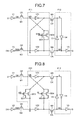
Fifth Embodiment
FIG. 7 is a circuit diagram illustrating a schematic configuration of a semiconductor integrated circuit according to the fifth embodiment of the present invention. In the semiconductor integrated circuit shown in FIG. 7, the state-holding circuit F31 shown in FIG. 5 is replaced by a state-holding circuit F41. In the state-holding circuit F41, the PMOS transistor M31 and the NMOS transistor M32 shown in FIG. 5 are not provided and the output of the inverter V31 is directly connected to the input of the inverter V32.
The data signal DBB is generated by inverting the inverted data signal DB in the inverter V2, so that the state change of the data signal DBB is delayed by the delay time by the inverter V2 from the state change of the inverted data signal DB. Therefore, the state change of the data signal D is transmitted to the storage node MB before the storage node M, and the state of the state-holding circuit F41 is determined in accordance with the state change of the storage node MB. Consequently, even when the PMOS transistor M31 and the NMOS transistor M32 shown in FIG. 5 are not provided in the state-holding circuit F41, the states held in the storage nodes M and MB can be easily transitioned.
Sixth Embodiment
FIG. 8 is a circuit diagram illustrating a schematic configuration of a semiconductor integrated circuit according to the sixth embodiment of the present invention. In the semiconductor integrated circuit shown in FIG. 8, the state-holding circuit F31 shown in FIG. 5 is replaced by a state-holding circuit F51. In the state-holding circuit F51, the gate of the PMOS transistor M31 and the gate of the NMOS transistor M32 are connected to the storage node MB, and the gate of the PMOS transistor M33 and the gate of the NMOS transistor M34 are connected to the storage node M.
When the PMOS transistors M1 and M2 are turned on, the inverted data signal DB is applied to the storage node MB and the data signal DBB is applied to the storage node M, so that the states held in the storage nodes M and MB can be easily transitioned similar to the third embodiment.
Seventh Embodiment
FIG. 9 is a circuit diagram illustrating a schematic configuration of a semiconductor integrated circuit according to the seventh embodiment of the present invention. In the semiconductor integrated circuit shown in FIG. 9, the PMOS transistors M1 and M2 shown in FIG. 5 are replaced by NMOS transistors M1′ and M2′ and the NMOS transistors M3 and M4 shown in FIG. 5 are replaced by PMOS transistors M3′ and M4′. A clock signal CKB is input to the gates of the NMOS transistors M1′ and M2′ and the gates of the PMOS transistors M3′ and M4′. The circuit shown in FIG. 5 triggers at the rising edge of the clock signal CK, whereas this circuit triggers at the falling edge of the clock signal CKB.
Then, the inverted data signal DB and the data signal DBB are input to the storage nodes MB and M via the NMOS transistors M1′ and M2′, respectively, and the output signal Q1 and the output inverted signal QB1 are output via the PMOS transistors M3′ and M4′, respectively. Whereby, it is possible to cause the state-holding circuit F31 to hold or transfer the state by inputting the clock signal CKB in the gates of the NMOS transistors M1′ and M2′ and the gates of the PMOS transistors M3′ and M4′.
Eighth Embodiment
FIG. 10 is a circuit diagram illustrating a schematic configuration of a semiconductor integrated circuit according to the eighth embodiment of the present invention. In the semiconductor integrated circuit shown in FIG. 10, the state-holding circuit F31 shown in FIG. 5 is replaced by a state-holding circuit F61. The state-holding circuit F61 includes inverters V61 to V64, PMOS transistors M61 and M64, and NMOS transistors M62 and M63.
The output of the inverter V61 is connected to the input of the inverter V62 via the PMOS transistor M61 and the NMOS transistor M62 that are connected in parallel to constitute the storage node M. The output of the inverter V62 is connected to the input of the inverter V61 via the PMOS transistor M64 and the NMOS transistor M63 that are connected in parallel to constitute the storage node MB. The inverted data signal DB is input to each gate of the PMOS transistor M61 and the NMOS transistor M62, and the data signal DBB is input to each gate of the PMOS transistor M64 and the NMOS transistor M63.
The storage node MB is connected to the drain of the PMOS transistor M1 and is connected to the drain of the NMOS transistor M3 via the inverter V63. The storage node M is connected to the drain of the PMOS transistor M2 and is connected to the drain of the NMOS transistor M4 via the inverter V64.
The inverters V61 and V62 in the eighth embodiment perform the data hold by the inverters V31 and V32 shown in FIG. 5, and the inverters V63 and V64 perform the data transmission by the inverters V31 and V32 shown in FIG. 5. The eighth embodiment can also obtain the effect similar to that in the third embodiment.
Ninth Embodiment
FIG. 11 is a circuit diagram illustrating a schematic configuration of a semiconductor integrated circuit according to the ninth embodiment of the present invention. In the semiconductor integrated circuit shown in FIG. 11, the state-holding circuit F31 shown in FIG. 5 is replaced by a state-holding circuit F71. The state-holding circuit F71 includes inverters V71 to V73, PMOS transistors M71 and M74, and NMOS transistors M72 and M73.
The output of the inverter V71 is connected to the input of the inverter V72 via the PMOS transistor M74 and the NMOS transistor M73 that are connected in parallel to constitute the storage node M. The output of the inverter V72 is connected to the input of the inverter V71 via the PMOS transistor M71 and the NMOS transistor M72 that are connected in parallel to constitute the storage node MB. The data signal DBB is input to each gate of the PMOS transistor M71 and the NMOS transistor M72, and the inverted data signal DB is input to each gate of the PMOS transistor M74 and the NMOS transistor M73.
The storage node MB is connected to the drain of the PMOS transistor M1 and is connected to the drain of the NMOS transistor M3 via the inverter V71. Moreover, the storage node M is connected to the drain of the PMOS transistor M2 and is connected to the drain of the NMOS transistor M4 via the inverter V73.
The inverter V71 performs the data hold and transmission by the inverter V31 shown in FIG. 5, the inverter V72 performs the data hold by the inverter V32 shown in FIG. 5, and the inverter V73 performs the data transmission by the inverter V32 shown in FIG. 5. The ninth embodiment can also obtain the effect similar to that in the third embodiment.
Tenth Embodiment
FIG. 12 is a circuit diagram illustrating a schematic configuration of a semiconductor integrated circuit according to the tenth embodiment of the present invention. In the semiconductor integrated circuit shown in FIG. 12, the inverter V2 shown in FIG. 5 is replaced by a PMOS transistor M5. The inverted data signal DB is input to the gate of the PMOS transistor M5. The source of the PMOS transistor M5 is connected to the high-level potential VDD and the drain of the PMOS transistor M5 is connected to the storage node M via the PMOS transistor M2.
When the inverted data signal DB is in a low level, the PMOS transistor M5 is turned on and the data signal DBB becomes a high level. Then, when the storage node MB is in a high level and the storage node M is in a low level, the storage node M is charged via the PMOS transistors M2 and M5. Therefore, the state-holding circuit F31 can be operated.
Eleventh Embodiment
FIG. 13 is a circuit diagram illustrating a schematic configuration of a semiconductor integrated circuit according to the eleventh embodiment of the present invention. The semiconductor integrated circuit shown in FIG. 13 includes a state-holding circuit F1 that holds two states, and the state-holding circuit F1 includes inverters V82 to V84, PMOS transistors M83 and M85, and NMOS transistors M84 and M86.
The output of the inverter V83 is connected to the input of the inverter V84 via the PMOS transistor M83 and the NMOS transistor M84 that are connected in parallel to constitute the storage node M. The output of the inverter V84 is connected to the input of the inverter V83 via the PMOS transistor M85 and the NMOS transistor M86 that are connected in parallel to constitute the storage node MB. The inverted data signal DB is input to each gate of the PMOS transistor M83 and the NMOS transistor M84, and the data signal DBB is input to each gate of the PMOS transistor M85 and the NMOS transistor M86. The storage node MB is connected to the input of the inverter V82.
Moreover, the semiconductor integrated circuit includes NMOS transistors M81, M82, M87, and M88. The NMOS transistors M81 and M82 are connected in series and the NMOS transistors M87 and M88 are connected in series. The storage node MB is connected to the output of the inverter V81 via the NMOS transistors M81 and M82. The storage node M is connected to the output of the inverter V85 via the NMOS transistors M87 and M88.
The clock signal CK is input to the gates of the NMOS transistors M82 and M87, and a inverted delayed clock signal CKB is input to the gates of the NMOS transistors M81 and M88. The inverted delayed clock signal CKB can be generated by delaying and inverting the clock signal CK in a clock buffer B1. The state change of the inverted delayed clock signal CKB is delayed by a delay time Td of the clock buffer 31 from the state change of the clock signal CK.
When the data signal D is input to the inverter V81, the inverted data signal DB is generated and is input to the source of the NMOS transistor M81 and the inverter V85. When the inverted data signal DB is input to the inverter V85, the data signal DBB is generated and is input to the source of the NMOS transistor M88.
Then, when the clock signal CK transitions from a low level to a high level, the inverted delayed clock signal CKB transitions from a high level to a low level after the delay time Td, so that the NMOS transistors M81, M82, M87, and M88 are all turned on only during the delay time Td.
When the NMOS transistors M81, M82, M87, and M88 are all turned on, the inverted data signal DB is applied to the storage node MB and the data signal DBB is applied to the storage node M. Then, the states of the storage nodes MB and M are held in accordance with the levels of the inverted data signal DB and the data signal DBB. Then, the state held in the storage node MB is inverted in the inverter V82 and is output as the output signal Q.
A parallel circuit of the PMOS transistor M83 and the NMOS transistor M84 is connected between the output of the inverter V83 and the input of the inverter V84, and a parallel circuit of the PMOS transistor M85 and the NMOS transistor M86 is connected between the output of the inverter V84 and the input of the inverter V83, so that the states held in the storage nodes M and MB can be easily transitioned and the operable power-supply voltage margin can be increased.
Twelfth Embodiment
FIG. 14 is a circuit diagram illustrating a schematic configuration of a semiconductor integrated circuit according to the twelfth embodiment of the present invention. In the semiconductor integrated circuit shown in FIG. 14, the state-holding circuit F31 shown in FIG. 5 is replaced by a state-holding circuit F91. The state-holding circuit F91 includes inverters V91 and V92, PMOS transistors M91 and M94, and NMOS transistors M92, M93, M95, and M96.
The PMOS transistor M91 and the NMOS transistors M92 and M93 are connected in series, and the PMOS transistor M94 and the NMOS transistors M95 and M96 are connected in series, between VDD-VSS. The gate of the PMOS transistor M94 and the gate of the NMOS transistor M96 are connected to the connection point of the NMOS transistors M92 and M93 to constitute the storage node MB. The gate of the PMOS transistor M91 and the gate of the NMOS transistor M93 are connected to the connection point of the NMOS transistors M95 and M96 to constitute the storage node M. The clock signal CK is input to the gates of the NMOS transistors M92 and M95.
The storage node MB is connected to the drain of the PMOS transistor M1 and is connected to the drain of the NMOS transistor M3 via the inverter V91. The storage node M is connected to the drain of the PMOS transistor M2 and is connected to the drain of the NMOS transistor M4 via the inverter V92.
When the clock signal CK is in a low level, the NMOS transistors M92 and M95 are off. Therefore, the storage nodes M and MB are both disconnected from the high-level potential VDD, so that the potentials of the storage nodes M and MB become undetermined.
On the other hand, when the clock signal CK is in a low level, the PMOS transistors M1 and M2 are on. Therefore, the inverted data signal DB is applied to the storage node MB and the data signal DBB is applied to the storage node M, so that the potential of the storage node MB is uniquely determined in accordance with the level of the inverted data signal DB and the potential of the storage node M is uniquely determined in accordance with the level of the data signal DBB.
Then, when the clock signal CK transitions from a low level to a high level, the NMOS transistors M3, M4, M92, and M95 are turned on. Therefore, any one of the storage nodes M and MB is connected to the high-level potential VDD in accordance with the levels of the data signal DBB and the inverted data signal DB, and the states in accordance with the levels of the data signal DBB and the inverted data signal DB are held in the storage nodes MB and M.
The states held in the storage nodes MB and M are inverted in the inverters V91 and V92, respectively, and are output as the output signal Q1 and the output inverted signal QB1 to the storage nodes S and SB via the NMOS transistors M3 and M4, respectively.
The holding capability of the states in the storage nodes M and MB can be lowered while the data signal DBB and the inverted data signal DB are applied to the storage nodes M and MB by the NMOS transistors M92 and M95, respectively, so that the states held in the storage nodes M and MB can be easily transitioned.
Moreover, the clock signal CK is input to the gates of the PMOS transistors M1 and M2 and the gates of the NMOS transistors M3, M4, M92, and M95, so that it is possible to cause the state-holding circuit F91 to hold or transfer the state. Therefore, there is no need to additionally provide a clock buffer that generates the clock inverted signal CKB from the clock signal CK, so that the power consumption can be reduced by the amount consumed by the clock buffer.
In the present embodiment in FIG. 14, explanation is given for the method in which the NMOS transistor M92 is inserted between the PMOS transistor M91 and the NMOS transistor M93 that constitutes the inverter; however, the NMOS transistor M92 can be inserted between the high-level potential VDD and the PMOS transistor M91.
Moreover, in the present embodiment in FIG. 14, explanation is given for the method in which the NMOS transistor M95 is inserted between the PMOS transistor M94 and the NMOS transistor M96 that constitutes the inverter; however, the NMOS transistor M95 can be inserted between the high-level potential VDD and the PMOS transistor M94.
Thirteenth Embodiment
FIG. 15 is a circuit diagram illustrating a schematic configuration of a semiconductor integrated circuit according to the thirteenth embodiment of the present invention. In the semiconductor integrated circuit shown in FIG. 15, protection circuits H1 and H2 and an inverter V6 are provided instead of the inverters V1 and V2 shown in FIG. 1. The protection circuits H1 and H2 can control input of the inverted data signal DB and the data signal DBB to the state-holding circuit F11 based on the state held in the state-holding circuit F11.
The protection circuit H1 includes PMOS transistors M101 and M102 and NMOS transistors M103 and M104. These transistors M101 to M104 are connected in series between VDD-VSS and the connection point of the PMOS transistor M102 and the NMOS transistor M103 is connected to the source of the PMOS transistor M1. The data signal D is input to each gate of the PMOS transistor M101 and the NMOS transistor M104, and the output inverted signal QB1 is input to each gate of the PMOS transistor M102 and the NMOS transistor M103.
The protection circuit H2 includes PMOS transistors M105 and M106 and NMOS transistors M107 and M108. These transistors M105 to M108 are connected in series between VDD-VSS and the connection point of the PMOS transistor M106 and the NMOS transistor M107 is connected to the source of the PMOS transistor M2. The inverted data signal DB is input to each gate of the PMOS transistor M105 and the NMOS transistor M108, and the output signal Q1 is input to each gate of the PMOS transistor M106 and the NMOS transistor M107. The gate of the NMOS transistor M108 is, connected to the output of the inverter V6.
The data signal D is input to the inverter V6, so that the inverted data signal DB is generated.
FIG. 16 is a diagram illustrating a timing difference in the state change between the data signal D and the inverted data signal DB. In FIG. 16, the inverted data signal DB is generated by inverting the data signal D in the inverter V6, so that the state change of the inverted data signal DB is delayed by the delay time by the inverter V6 from the state change of the data signal D.
Therefore, even when the PMOS transistors M101 and M105 are turned on at the same time due to the timing difference in the state change between the data signal D and the inverted data signal DB, it is possible to prevent the charging paths to the storage nodes MB and M from being formed at the same time. Moreover, even when the NMOS transistors M104 and M108 are turned on at the same time, it is possible to prevent the discharging paths from the storage nodes MB and M from being formed at the same time.
Consequently, even when there is the timing difference in the state change between the data signal D and the inverted data signal DB, it is possible to discharge from any one of the storage nodes MB and M and charge to the other of the storage nodes MB and M, so that data writing to the storage nodes MB and M can be normally performed.
Fourteenth Embodiment
FIG. 17 is a circuit diagram illustrating a schematic configuration of a semiconductor integrated circuit according to the fourteenth embodiment of the present invention. In the semiconductor integrated circuit shown in FIG. 17, the protection circuit H2 shown in FIG. 15 is provided instead of the inverter V2 shown in FIG. 1. The protection circuit H2 is provided only on the side of the storage node M, so that even when there is the timing difference in the state change between the data signal D and the inverted data signal DB, it is possible to prevent the charging paths to the storage nodes MB and M from being formed at the same time and prevent the discharging paths from the storage nodes MB and M from being formed at the same time. Thus, data writing to the storage nodes MB and M can be normally performed.
Fifteenth Embodiment
FIG. 18 is a circuit diagram illustrating a schematic configuration of a semiconductor integrated circuit according to the fifteenth embodiment of the present invention. In the semiconductor integrated circuit shown in FIG. 18, the state-holding circuit F11 shown in FIG. 17 is replaced by a state-holding circuit F101. The state-holding circuit F101 includes inverters V101 to V103.
The output of the inverter V101 is connected to the input of the inverter V102 to constitute the storage node MB, and the output of the inverter V102 is connected to the input of the inverter V101 to constitute the storage node M.
The storage node MB is connected to the drain of the PMOS transistor M1 and is connected to the drain of the NMOS transistor M3 via the inverter V91. The storage node M is connected to the drain of the PMOS transistor M2 and is connected to the drain of the NMOS transistor M4 via the inverter V103.
The inverter V102 performs the data hold and transmission by the inverters V12 and V13 shown in FIG. 17, the inverter V101 performs the data hold by the inverter V11 shown in FIG. 17, and the inverter V103 performs the data transmission by the inverter V14 shown in FIG. 17. The fifteenth embodiment can also obtain the effect similar to that in the fourteenth embodiment.
Sixteenth Embodiment
FIG. 19 is a circuit diagram illustrating a schematic configuration of a semiconductor integrated circuit according to the sixteenth embodiment of the present invention. In the semiconductor integrated circuit shown in FIG. 19, the state-holding circuit F11 shown in FIG. 17 is replaced by a state-holding circuit F111. The state-holding circuit F111 includes clocked gates V111 and V112. The output of the clocked gate V111 is connected to the input of the clocked gate V112 to constitute the storage node M, and the output of the clocked gate V112 is connected to the input of the clocked gate V111 to constitute the storage node MB. The storage node MB is connected to each drain of the PMOS transistor M1 and the NMOS transistor M4. The storage node M is connected to each drain of the PMOS transistor M2 and the NMOS transistor M3.
In the clocked gates V111 and V112, a PMOS transistor M111 and NMOS transistors M112 and M113 that are connected in series are provided. The gate of the PMOS transistor M111 and the gate of the NMOS transistor M112 are connected in common, and the clock signal CK is input to the gate of the NMOS transistor M113.
When the clock signal CK is in a low level, the NMOS transistor M113 is off. Therefore, the low-level potential VSS is not supplied to both of the storage nodes M and MB, so that the potentials of the storage nodes M and MB become undetermined.
On the other hand, when the clock signal CK is in a low level, the PMOS transistors M1 and M2 are on. Therefore, the inverted data signal DB is applied to the storage node MB and the data signal DBB is applied to the storage node M. The potential of the storage node MB is uniquely determined in accordance with the level of the inverted data signal DB and the potential of the storage node M is uniquely determined in accordance with the level of the data signal DBB.
Then, when the clock signal CK transitions from a low level to a high level, the NMOS transistor M113 is turned on. Therefore, the low-level potential VSS is supplied to the storage nodes M and MB, and the states in accordance with the levels of the data signal DBB and the inverted data signal DB are held in the storage nodes MB and M.
The states held in the storage nodes M and MB are output as the output signal Q1 and the output inverted signal QB1 to the storage nodes S and SB via the NMOS transistors M3 and M4, respectively.
The holding capability of the states in the storage nodes M and MB can be lowered while the data signal DBB and the inverted data signal DB are applied to the storage nodes M and MB, respectively, by constituting the state-holding circuit F111 by the clocked gates V111 and V112, so that the states held in the storage nodes M and MB can be easily transitioned.
Moreover, it is possible to cause the state-holding circuit F111 to hold or transfer the state by inputting the clock signal CK to each gate of the PMOS transistors M1 and M2 and the NMOS transistors M3, M4, and M113. Therefore, there is no need to additionally provide a clock buffer that generates the clock inverted signal CKB from the clock signal CK, so that the power consumption can be reduced by the amount consumed by the clock buffer.
In the present embodiment in FIG. 19, explanation is given for the method in which the NMOS transistor M113 is connected to the source of the NMOS transistor M112; however, the NMOS transistor M113 can be connected to the source of the PMOS transistor M111 or the NMOS transistor M113 can be inserted between the PMOS transistor M111 and the NMOS transistor M112.
Seventeenth Embodiment
FIG. 20 is a circuit diagram illustrating a schematic configuration of a semiconductor integrated circuit according to the seventeenth embodiment of the present invention. In the semiconductor integrated circuit shown in FIG. 20, the state-holding circuit F1 shown in FIG. 13 is replaced by a state-holding circuit F2. The state-holding circuit F2 includes the inverters V82 to V84.
The output of the inverter V83 is connected to the input of the inverter V84 to constitute the storage node M, and the output of the inverter V84 is connected to the input of the inverter V83 to constitute the storage node MB.
Therefore, the state of the state-holding circuit F2 can be changed only during the period defined by the delay time Td of the clock buffer S1, thus enabling to perform a pulse trigger operation. Thus, even when the storage nodes MB and M are pulled down and pulled up by using the inverted data signal DB and the data signal DBB, the operation speed can be improved.
Moreover, the protection circuit H2 is provided on the side of the storage node M, so that even when there is the timing difference in the state change between the data signal DBB and the inverted data signal DB, data writing to the storage nodes MB and M can be normally performed.
The embodiments of the present invention are explained as described above; however, the circuit according to the embodiments of the present invention can be used, for example, in a high performance LSI such as an LSI for digital terrestrial broadcast reception. Typically, in the high performance LSI, a flip-flop circuit occupies about 30% to 40% of the whole. Therefore, the switching power or the operation power can be reduced by applying the flip-flop circuit in the present embodiments to the high performance LSI.
Moreover, in the case where all of the circuit blocks in an LSI operate, even when a technology such as power shutdown cannot be used, the operation power can be reduced by using the flip-flop circuit in the present embodiments.
Furthermore, the flip-flop circuit in the present embodiments can be mixed with other power-saving technologies such as clock gating, power shutdown, multiple supply voltages, or dynamic voltage frequency scaling (DVFS).
Additional advantages and modifications will readily occur to those skilled in the art. Therefore, the invention in its broader aspects is not limited to the specific details and representative embodiments shown and described herein. Accordingly, various modifications may be made without departing from the spirit or scope of the general inventive concept as defined by the appended claims and their equivalents.

Claims (20)

What is claimed is:
1. A semiconductor integrated circuit comprising:
a state holding circuit that inputs an output of one inverter to another inverter with each other;
an input circuit that causes a state of the state holding circuit to transition based on a data signal;
a first first-conductive transistor that is inserted between an input of the one inverter and an output of the another inverter and is controlled by the data signal;
a first second-conductive transistor that is connected in parallel with the first first-conductive transistor and is controlled by the data signal;
a first P-channel field-effect transistor that inputs a data signal to the one inverter of the state holding circuit when a clock signal is in a low level;
a second P-channel field-effect transistor that inputs an inverted data signal to the another inverter of the state holding circuit when the clock signal is in a low level;
a first N-channel field-effect transistor that transmits one state held in the state holding circuit when the clock signal is in a high level; and
a second N-channel field-effect transistor that transmits another state held in the state holding circuit when the clock signal is in a high level, wherein
a gate of the first first-conductive transistor and a gate of the first second-conductive transistor are directly connected to a same node.
2. The semiconductor integrated circuit according to claim 1, wherein the state holding circuit includes
a first inverter of which output is connected to a drain of the first P-channel field-effect transistor and of which input is connected to a drain of the second P-channel field-effect transistor,
a second inverter of which input is connected to the drain of the first P-channel field-effect transistor and of which output is connected to the drain of the second P-channel field-effect transistor,
a third inverter of which input is connected to the drain of the first P-channel field-effect transistor and of which output is connected to a drain of the first N-channel field-effect transistor, and
a fourth inverter of which input is connected to the drain of the second P-channel field-effect transistor and of which output is connected to a drain of the second N-channel field-effect transistor.
3. The semiconductor integrated circuit according to claim 1, wherein the state holding circuit includes
a first inverter of which input is connected to a drain of the first P-channel field-effect transistor and a drain of the second N-channel field-effect transistor and of which output is connected to a drain of the second P-channel field-effect transistor and a drain of the first N-channel field-effect transistor, and
a second inverter of which input is connected to the drain of the second P-channel field-effect transistor and the drain of the first N-channel field-effect transistor and of which output is connected to the drain of the first P-channel field-effect transistor and the drain of the second N-channel field-effect transistor.
4. The semiconductor integrated circuit according to claim 1, wherein the state holding circuit includes
a first inverter of which output is connected to a drain of the first P-channel field-effect transistor and of which input is connected to a drain of the second P-channel field-effect transistor,
a second inverter of which input is connected to the drain of the first P-channel field-effect transistor and of which output is connected to a drain of the first N-channel field-effect transistor, and
a third inverter of which input is connected to the drain of the second P-channel field-effect transistor and the drain of the first N-channel field-effect transistor and of which output is connected to a drain of the second N-channel field-effect transistor.
5. The semiconductor integrated circuit according to claim 1, further comprising:
a third P-channel field-effect transistor that is inserted between an input of the one inverter and an output of the another inverter of the state holding circuit and is turned on when the data signal is in a low level; and
a third N-channel field-effect transistor that is connected in parallel with the third P-channel field-effect transistor and is turned on when the data signal is in a high level.
6. The semiconductor integrated circuit according to claim 1, further comprising:
a third P-channel field-effect transistor that is inserted between an input of the one inverter and an output of the another inverter of the state holding circuit and is turned on when the one state of the state holding circuit is in a low level; and
a third N-channel field-effect transistor that is connected in parallel with the third P-channel field-effect transistor and is turned on when the another state of the state holding circuit is in a high level.
7. The semiconductor integrated circuit according to claim 1, further comprising a fourth P-channel field-effect transistor that is provided between a source of the second P-channel field-effect transistor and a power-supply voltage node and is turned on when an input signal is in a low level.
8. The semiconductor integrated circuit according to claim 1, further comprising a protection circuit that controls an input of the data signal to the state holding circuit based on a state held in the state holding circuit.
9. The semiconductor integrated circuit according to claim 8, wherein the protection circuit includes
a third P-channel field-effect transistor that operates based on the data signal;
a fourth P-channel field-effect transistor that is connected in series with the third P-channel field-effect transistor and operates based on the state of the state holding circuit,
a third N-channel field-effect transistor that is connected in series with the fourth P-channel field-effect transistor and operates based on the state of the state holding circuit, and
a fourth N-channel field-effect transistor that is connected in series with the third N-channel field-effect transistor and operates based on the data signal.
10. The semiconductor integrated circuit according to claim 1, further comprising a third N-channel field-effect transistor that is inserted in a charging path of the one inverter of the state holding circuit and renders the charging path conductive when the clock signal is in a high level.
11. The semiconductor integrated circuit according to claim 1, further comprising:
a fourth N-channel field-effect transistor that is connected in series with a third P-channel field-effect transistor or a third N-channel field-effect transistor that constitutes the one inverter of the state holding circuit and is turned on when the clock signal is in a high level; and
a sixth N-channel field-effect transistor that is connected in series with a fourth P-channel field-effect transistor or a fifth N-channel field-effect transistor that constitutes the another inverter of the state holding circuit and is turned on when the clock signal is in a high level.
12. The semiconductor integrated circuit according to claim 1, further comprising:
a first N-channel field-effect transistor that inputs a data signal to the one inverter of the state holding circuit when a clock signal is in a high level;
a second N-channel field-effect transistor that inputs an inverted data signal to the another inverter of the state holding circuit when the clock signal is in a high level;
a first P-channel field-effect transistor that transmits one state held in the state holding circuit when the clock signal is in a low level; and
a second P-channel field-effect transistor that transmits another state held in the state holding circuit when the clock signal is in a low level.
13. The semiconductor integrated circuit according to claim 12, further comprising:
a third P-channel field-effect transistor that is inserted between an input of the one inverter and an output of the another inverter of the state holding circuit and is turned on when the data signal is in a low level; and
a third N-channel field-effect transistor that is connected in parallel with the third P-channel field-effect transistor and is turned on when the data signal is in a high level.
14. The semiconductor integrated circuit according to claim 12, further comprising:
a third P-channel field-effect transistor that is inserted between an input of the one inverter and an output of the another inverter of the state holding circuit and is turned on when the one state of the state holding circuit is in a low level; and
a third N-channel field-effect transistor that is connected in parallel with the third P-channel field-effect transistor and is turned on when the another state of the state holding circuit is in a high level.
15. The semiconductor integrated circuit according to claim 1, further comprising a clock buffer that generates an inverted delayed clock signal that is obtained by inverting the clock signal with delay, wherein
the input circuit includes a first switch and a second switch,
the first switch includes
a second N-channel field-effect transistor that is provided on a side of one storage node of the state holding circuit and is turned on when the clock signal is in a high level, and
a third N-channel field-effect transistor that is connected in series with the second N-channel field-effect transistor and is turned on when the inverted delayed clock signal is in a high level, and
the second switch includes
a fourth N-channel field-effect transistor that is provided on a side of another storage node of the state holding circuit and is turned on when the clock signal is in a high level, and
a fifth N-channel field-effect transistor that is connected in series with the fourth N-channel field-effect transistor and is turned on when the inverted delayed clock signal is in a high level.
16. The semiconductor integrated circuit according to claim 15, wherein the state of the state holding circuit is capable of being changed only during a period defined in a delay time of the clock buffer.
17. A semiconductor integrated circuit comprising:
a state holding circuit that holds two states by inputting an output of one inverter to another inverter with each other;
a first P-channel field-effect transistor that inputs a data signal to the one inverter of the state holding circuit when a clock signal is in a low level;
a second P-channel field-effect transistor that inputs an inverted data signal to the another inverter of the state holding circuit when the clock signal is in a low level;
a first N-channel field-effect transistor that transmits one state outputted from the one inverter when the clock signal is in a high level; and
a second N-channel field-effect transistor that transmits another state outputted from the another inverter when the clock signal is in a high level,
a first first-conductive transistor that is inserted between an input of the one inverter and an output of the another inverter and a gate of the first first-conductive transistor is connected to the first node; and
a first second-conductive transistor that is connected in parallel with the first first-conductive transistor and a gate of the first second-conductive transistor is connected to the first node, wherein
the one inverter is connected between the first P-channel field-effect transistor and the first N-channel field-effect transistor, and the another inverter is connected between the second P-channel field-effect transistor and the second N-channel field-effect transistor, and wherein
the output terminal of the one inverter is directly connected to the input terminal of the another inverter, and the output terminal of the another inverter is directly connected to the input terminal of the one inverter.
18. A semiconductor integrated circuit comprising:
a state holding circuit that holds two states by inputting an output of one inverter to another inverter with each other;
a first N-channel field-effect transistor that inputs a data signal to the one inverter of the state holding circuit when a clock signal is in a high level;
a second N-channel field-effect transistor that inputs an inverted data signal to the another inverter of the state holding circuit when the clock signal is in a high level;
a first P-channel field-effect transistor that transmits one state outputted from the one inverter when the clock signal is in a low level; and
a second P-channel field-effect transistor that transmits another state outputted from the another inverter when the clock signal is in a low level,
a first first-conductive transistor that is inserted between an input of the one inverter and an output of the another inverter and a gate of the first first-conductive transistor is connected to the first node; and
a first second-conductive transistor that is connected in parallel with the first first-conductive transistor and a gate of the first second-conductive transistor is connected to the first node, wherein
the one inverter is connected between the first N-channel field-effect transistor and the first P-channel field-effect transistor, and the another inverter is connected between the second N-channel field-effect transistor and the second P-channel field-effect transistor, and wherein
the output terminal of the one inverter is directly connected to the input terminal of the another inverter, and the output terminal of the another inverter is directly connected to the input terminal of the one inverter.
19. A semiconductor integrated circuit comprising:
a state holding circuit that inputs an output of one inverter to another inverter with each other;
a switch to which a first data signal is inputted at a first node and outputs a second data signal synchronized with a clock signal and causes a state of the state holding circuit to transition based on the second data signal;
a first first-conductive transistor that is inserted between an input of the one inverter and an output of the another inverter and a gate of the first first-conductive transistor is connected to the first node; and
a first second-conductive transistor that is connected in parallel with the first first-conductive transistor and a gate of the first second-conductive transistor is connected to the first node.
20. A semiconductor integrated circuit comprising:
a state holding circuit that inputs an output of one inverter to another inverter with each other;
a switch to which a first data signal is inputted at a first node and outputs a second data signal synchronized with a clock signal and causes a state of the state holding circuit to transition based on the second data signal;
a first transistor that is inserted between an input of the one inverter and an output of the another inverter and a gate of the first transistor is connected to the first node; and
a second transistor that is inserted between an output of the one inverter and an input of the another inverter and a gate of the second transistor is connected to a second node which is driven by an inverted logical state of the first data signal.
US12/722,837 2009-07-23 2010-03-12 Semiconductor integrated circuit Active 2031-01-05 US8519743B2 (en)

Priority Applications (1)

Application Number Priority Date Filing Date Title
US13/948,778 US9106225B2 (en) 2009-07-23 2013-07-23 Semiconductor integrated circuit

Applications Claiming Priority (2)

Application Number Priority Date Filing Date Title
JP2009172278A JP5284211B2 (en) 2009-07-23 2009-07-23 Semiconductor integrated circuit
JP2009-172278 2009-07-23

Related Child Applications (1)

Application Number Title Priority Date Filing Date
US13/948,778 Division US9106225B2 (en) 2009-07-23 2013-07-23 Semiconductor integrated circuit

Publications (2)

Publication Number Publication Date
US20110018584A1 US20110018584A1 (en) 2011-01-27
US8519743B2 true US8519743B2 (en) 2013-08-27

Family

ID=43496747

Family Applications (2)

Application Number Title Priority Date Filing Date
US12/722,837 Active 2031-01-05 US8519743B2 (en) 2009-07-23 2010-03-12 Semiconductor integrated circuit
US13/948,778 Active 2030-05-17 US9106225B2 (en) 2009-07-23 2013-07-23 Semiconductor integrated circuit

Family Applications After (1)

Application Number Title Priority Date Filing Date
US13/948,778 Active 2030-05-17 US9106225B2 (en) 2009-07-23 2013-07-23 Semiconductor integrated circuit

Country Status (2)

Country Link
US (2) US8519743B2 (en)
JP (1) JP5284211B2 (en)

Cited By (6)

* Cited by examiner, † Cited by third party
Publication number Priority date Publication date Assignee Title
US20140312950A1 (en) * 2013-04-22 2014-10-23 Fujitsu Limited Data holding circuit and semiconductor integrated circuit device
US8941428B2 (en) 2012-11-05 2015-01-27 Arm Limited Low power latching circuits
US9281807B1 (en) * 2014-06-09 2016-03-08 Xilinx, Inc. Master-slave flip-flops and methods of implementing master-slave flip-flops in an integrated circuit
US10497335B2 (en) * 2016-11-21 2019-12-03 Lg Display Co., Ltd. Display device
US11336271B2 (en) * 2018-10-16 2022-05-17 Sony Semiconductor Solutions Corporation Data holding circuit
US20230238960A1 (en) * 2022-01-26 2023-07-27 Airoha Technology Corp. Output driver using feedback network for slew rate reduction and associated output driving method

Families Citing this family (2)

* Cited by examiner, † Cited by third party
Publication number Priority date Publication date Assignee Title
CN103888106B (en) * 2014-03-31 2017-01-11 西安空间无线电技术研究所 Method for designing trigger resistant to single event upset and single event transient pulses
US10110214B2 (en) * 2017-01-11 2018-10-23 Stmicroelectronics (Research & Development) Limited Voltage comparator circuit including a plurality of voltage controlled delay lines

Citations (11)

* Cited by examiner, † Cited by third party
Publication number Priority date Publication date Assignee Title
US4096401A (en) * 1977-05-12 1978-06-20 Rca Corporation Sense circuit for an MNOS array using a pair of CMOS inverters cross-coupled via CMOS gates which are responsive to the input sense signals
US4506167A (en) * 1982-05-26 1985-03-19 Motorola, Inc. High speed logic flip-flop latching arrangements including input and feedback pairs of transmission gates
JPS6240816A (en) 1985-08-16 1987-02-21 Toshiba Corp Latching circuit, and flip-flop circuit using this latching circuit
US4939384A (en) * 1988-10-03 1990-07-03 Oki Electric Industry Co., Ltd Flip-flop circuit
JPH03262317A (en) 1990-03-13 1991-11-22 Nec Corp Flip-flop circuit
US5654659A (en) * 1994-02-28 1997-08-05 Nec Corporation Scan circuit having a reduced clock signal delay
JPH09232919A (en) 1996-02-23 1997-09-05 Nippon Telegr & Teleph Corp <Ntt> Latch circuit and flip-flop circuit
JPH09232920A (en) 1996-02-28 1997-09-05 Nec Ic Microcomput Syst Ltd Flip-flop circuit
JPH10190416A (en) 1996-12-24 1998-07-21 Toshiba Corp Flip-flop circuit
US20040095175A1 (en) * 2002-11-18 2004-05-20 Procket Networks, Inc. Flip-flop circuit with reduced power consumption
US7109772B2 (en) * 2002-10-31 2006-09-19 Infineon Technologies Ag D-type flipflop

Family Cites Families (6)

* Cited by examiner, † Cited by third party
Publication number Priority date Publication date Assignee Title
JPS6240616A (en) 1985-08-16 1987-02-21 Kao Corp Binder for magnetic recording medium and magnetic recording medium
JP2540934B2 (en) * 1989-03-09 1996-10-09 三菱電機株式会社 Logic circuit device
JPH10109416A (en) 1996-10-07 1998-04-28 Seiko Epson Corp Piezoelectric oscillator unit for ink jet type recording head and manufacture thereof
JP3519001B2 (en) * 1998-10-15 2004-04-12 シャープ株式会社 Latch circuit and flip-flop circuit
US6417711B2 (en) * 1999-10-19 2002-07-09 Honeywell Inc. High speed latch and flip-flop
US7196550B1 (en) * 2003-06-26 2007-03-27 Cypress Semiconductor Corporation Complementary CMOS driver circuit with de-skew control

Patent Citations (12)

* Cited by examiner, † Cited by third party
Publication number Priority date Publication date Assignee Title
US4096401A (en) * 1977-05-12 1978-06-20 Rca Corporation Sense circuit for an MNOS array using a pair of CMOS inverters cross-coupled via CMOS gates which are responsive to the input sense signals
US4506167A (en) * 1982-05-26 1985-03-19 Motorola, Inc. High speed logic flip-flop latching arrangements including input and feedback pairs of transmission gates
JPS6240816A (en) 1985-08-16 1987-02-21 Toshiba Corp Latching circuit, and flip-flop circuit using this latching circuit
US4939384A (en) * 1988-10-03 1990-07-03 Oki Electric Industry Co., Ltd Flip-flop circuit
JPH03262317A (en) 1990-03-13 1991-11-22 Nec Corp Flip-flop circuit
US5654659A (en) * 1994-02-28 1997-08-05 Nec Corporation Scan circuit having a reduced clock signal delay
JPH09232919A (en) 1996-02-23 1997-09-05 Nippon Telegr & Teleph Corp <Ntt> Latch circuit and flip-flop circuit
JPH09232920A (en) 1996-02-28 1997-09-05 Nec Ic Microcomput Syst Ltd Flip-flop circuit
JPH10190416A (en) 1996-12-24 1998-07-21 Toshiba Corp Flip-flop circuit
US7109772B2 (en) * 2002-10-31 2006-09-19 Infineon Technologies Ag D-type flipflop
US20040095175A1 (en) * 2002-11-18 2004-05-20 Procket Networks, Inc. Flip-flop circuit with reduced power consumption
US6864732B2 (en) * 2002-11-18 2005-03-08 Procket Networks, Inc. Flip-flop circuit with reduced power consumption

Non-Patent Citations (1)

* Cited by examiner, † Cited by third party
Title
Japanese Office Action for Japanese Application No. 2009-172278 mailed on Sep. 11, 2012.

Cited By (7)

* Cited by examiner, † Cited by third party
Publication number Priority date Publication date Assignee Title
US8941428B2 (en) 2012-11-05 2015-01-27 Arm Limited Low power latching circuits
US20140312950A1 (en) * 2013-04-22 2014-10-23 Fujitsu Limited Data holding circuit and semiconductor integrated circuit device
US9130555B2 (en) * 2013-04-22 2015-09-08 Fujitsu Limited Data holding circuit and semiconductor integrated circuit device
US9281807B1 (en) * 2014-06-09 2016-03-08 Xilinx, Inc. Master-slave flip-flops and methods of implementing master-slave flip-flops in an integrated circuit
US10497335B2 (en) * 2016-11-21 2019-12-03 Lg Display Co., Ltd. Display device
US11336271B2 (en) * 2018-10-16 2022-05-17 Sony Semiconductor Solutions Corporation Data holding circuit
US20230238960A1 (en) * 2022-01-26 2023-07-27 Airoha Technology Corp. Output driver using feedback network for slew rate reduction and associated output driving method

Also Published As

Publication number Publication date
JP2011029828A (en) 2011-02-10
US20130307585A1 (en) 2013-11-21
JP5284211B2 (en) 2013-09-11
US9106225B2 (en) 2015-08-11
US20110018584A1 (en) 2011-01-27

Similar Documents

Publication Publication Date Title
US9106225B2 (en) Semiconductor integrated circuit
JP4262053B2 (en) MTCMOS flip-flop circuit that can store data in sleep mode
US7405606B2 (en) D flip-flop
JP3614125B2 (en) CP flip-flop
US7804346B2 (en) Level converting flip-flop and method of operating the same
US20100060319A1 (en) Low leakage and data retention circuitry
US20080238514A1 (en) Level-converted and clock-gated latch and sequential logic circuit having the same
US7456669B2 (en) Semiconductor integrated circuit device
JPH0964715A (en) Semiconductor integrated circuit
TW201429163A (en) Clock gating latch, method of operation thereof and integrated circuit employing the same
JPH11112297A (en) Latch circuit and semiconductor integrated circuit having the same
US7440534B2 (en) Master-slave flip-flop, trigger flip-flop and counter
US7427875B2 (en) Flip-flop circuit
US8008959B2 (en) Flip-flop circuit that latches inputted data
US6836175B2 (en) Semiconductor integrated circuit with sleep memory
KR100922696B1 (en) Clock based data storage element and dual pulse generation element and data storage element
US6518790B2 (en) Semiconductor integrated circuit having circuit for transmitting input signal
US10355672B2 (en) Semiconductor device with power gating scheme
KR102024470B1 (en) Low Power Flip-Flop
US11575366B2 (en) Low power flip-flop
US20080030250A1 (en) Flip-flop circuit
US10706916B1 (en) Method and apparatus for integrated level-shifter and memory clock
US6407604B1 (en) Register and latch circuits
JP3033719B2 (en) Low power semiconductor integrated circuit
KR100699448B1 (en) High-Credibility Flip-Flop and Mult-Threshold CMOS Latch Circuit Having Low Sub-Threshold Leakage Current

Legal Events

Date Code Title Description
AS Assignment

Owner name: KABUSHIKI KAISHA TOSHIBA, JAPAN

Free format text: ASSIGNMENT OF ASSIGNORS INTEREST;ASSIGNORS:TEH, CHEN KONG;HARA, HIROYUKI;REEL/FRAME:024072/0906

Effective date: 20100305

STCF Information on status: patent grant

Free format text: PATENTED CASE

FEPP Fee payment procedure

Free format text: PAYOR NUMBER ASSIGNED (ORIGINAL EVENT CODE: ASPN); ENTITY STATUS OF PATENT OWNER: LARGE ENTITY

FPAY Fee payment

Year of fee payment: 4

MAFP Maintenance fee payment

Free format text: PAYMENT OF MAINTENANCE FEE, 8TH YEAR, LARGE ENTITY (ORIGINAL EVENT CODE: M1552); ENTITY STATUS OF PATENT OWNER: LARGE ENTITY

Year of fee payment: 8