US8470454B2 - Material for organic photoelectric device and organic photoelectric device including the same - Google Patents
Material for organic photoelectric device and organic photoelectric device including the same Download PDFInfo
- Publication number
- US8470454B2 US8470454B2 US13/033,842 US201113033842A US8470454B2 US 8470454 B2 US8470454 B2 US 8470454B2 US 201113033842 A US201113033842 A US 201113033842A US 8470454 B2 US8470454 B2 US 8470454B2
- Authority
- US
- United States
- Prior art keywords
- organic
- photoelectric device
- organic photoelectric
- layer
- substituted
- Prior art date
- Legal status (The legal status is an assumption and is not a legal conclusion. Google has not performed a legal analysis and makes no representation as to the accuracy of the status listed.)
- Active
Links
- PVQSJGTZLUTCHT-UHFFFAOYSA-N C1=CC2=CC=CC(C3=NC(C4=CC=C(C5=NC=CC6=C5C=CC=C6)C=C4)=NC(C4=CC=C(C5=NC=CC6=C5C=CC=C6)C=C4)=C3)=C2C=C1.C1=CC=C(C2=NC(C3=CC=C(C4=NC=CC5=C4C=CC=C5)C=C3)=NC(C3=CC=C(C4=NC=CC5=C4C=CC=C5)C=C3)=C2)C=C1.C1=CN=C(C2=CC=C(C3=CC(C4=C5/C=C\C6=CC=CC7=CC=C(C=C4)C5C76)=NC(C4=CC=C(C5=NC=CC=C5)C=C4)=N3)C=C2)C=C1.C1=CN=C(C2=CC=C(C3=CC(C4=CC5=C(C=CC=C5)C5=C4C=CC=C5)=NC(C4=CC=C(C5=NC=CC=C5)C=C4)=N3)C=C2)C=C1 Chemical compound C1=CC2=CC=CC(C3=NC(C4=CC=C(C5=NC=CC6=C5C=CC=C6)C=C4)=NC(C4=CC=C(C5=NC=CC6=C5C=CC=C6)C=C4)=C3)=C2C=C1.C1=CC=C(C2=NC(C3=CC=C(C4=NC=CC5=C4C=CC=C5)C=C3)=NC(C3=CC=C(C4=NC=CC5=C4C=CC=C5)C=C3)=C2)C=C1.C1=CN=C(C2=CC=C(C3=CC(C4=C5/C=C\C6=CC=CC7=CC=C(C=C4)C5C76)=NC(C4=CC=C(C5=NC=CC=C5)C=C4)=N3)C=C2)C=C1.C1=CN=C(C2=CC=C(C3=CC(C4=CC5=C(C=CC=C5)C5=C4C=CC=C5)=NC(C4=CC=C(C5=NC=CC=C5)C=C4)=N3)C=C2)C=C1 PVQSJGTZLUTCHT-UHFFFAOYSA-N 0.000 description 5
- GEWFNTYNUIZJLP-UHFFFAOYSA-N C1=CC=C(C2=C3C=CC=CC3=C(C3=NC(C4=CC=C(C5=NC=CC=C5)C=C4)=NC(C4=CC=C(C5=NC=CC=C5)C=C4)=C3)C3=C2C=CC=C3)C=C1.C1=CN=C(C2=CC=C(C3=CC(C4=C5C=CC=CC5=C(C5=C6C=CC=CC6=CC=C5)C5=C4C=CC=C5)=NC(C4=CC=C(C5=NC=CC=C5)C=C4)=N3)C=C2)C=C1.C1=CN=C(C2=CC=C(C3=CC(C4=C5C=CC=CC5=C(C5=CC6=C(C=CC=C6)C=C5)C5=C4C=CC=C5)=NC(C4=CC=C(C5=NC=CC=C5)C=C4)=N3)C=C2)C=C1 Chemical compound C1=CC=C(C2=C3C=CC=CC3=C(C3=NC(C4=CC=C(C5=NC=CC=C5)C=C4)=NC(C4=CC=C(C5=NC=CC=C5)C=C4)=C3)C3=C2C=CC=C3)C=C1.C1=CN=C(C2=CC=C(C3=CC(C4=C5C=CC=CC5=C(C5=C6C=CC=CC6=CC=C5)C5=C4C=CC=C5)=NC(C4=CC=C(C5=NC=CC=C5)C=C4)=N3)C=C2)C=C1.C1=CN=C(C2=CC=C(C3=CC(C4=C5C=CC=CC5=C(C5=CC6=C(C=CC=C6)C=C5)C5=C4C=CC=C5)=NC(C4=CC=C(C5=NC=CC=C5)C=C4)=N3)C=C2)C=C1 GEWFNTYNUIZJLP-UHFFFAOYSA-N 0.000 description 5
- XVZPJGJBAXSYSI-UHFFFAOYSA-N C1=CC=C(C2=NC(C3=CC=C(C4=NC=CC=C4)C=C3)=NC(C3=CC=C(C4=NC=CC=C4)C=C3)=C2)C=C1.C1=CN=C(C2=CC=C(C3=CC(C4=C5C=CC=CC5=CC5=C4C=CC=C5)=NC(C4=CC=C(C5=NC=CC=C5)C=C4)=N3)C=C2)C=C1.C1=CN=C(C2=CC=C(C3=CC(C4=C5C=CC=CC5=CC=C4)=NC(C4=CC=C(C5=NC=CC=C5)C=C4)=N3)C=C2)C=C1.C1=CN=C(C2=CC=C(C3=CC(C4=CC5=C(C=CC=C5)C=C4)=NC(C4=CC=C(C5=NC=CC=C5)C=C4)=N3)C=C2)C=C1 Chemical compound C1=CC=C(C2=NC(C3=CC=C(C4=NC=CC=C4)C=C3)=NC(C3=CC=C(C4=NC=CC=C4)C=C3)=C2)C=C1.C1=CN=C(C2=CC=C(C3=CC(C4=C5C=CC=CC5=CC5=C4C=CC=C5)=NC(C4=CC=C(C5=NC=CC=C5)C=C4)=N3)C=C2)C=C1.C1=CN=C(C2=CC=C(C3=CC(C4=C5C=CC=CC5=CC=C4)=NC(C4=CC=C(C5=NC=CC=C5)C=C4)=N3)C=C2)C=C1.C1=CN=C(C2=CC=C(C3=CC(C4=CC5=C(C=CC=C5)C=C4)=NC(C4=CC=C(C5=NC=CC=C5)C=C4)=N3)C=C2)C=C1 XVZPJGJBAXSYSI-UHFFFAOYSA-N 0.000 description 5
- JQWOZZYAMDEPIW-UHFFFAOYSA-N C1=CC=C2C(=C1)C1=C(C=CC=C1)N2C1=CC=C(C2=CC(C3=C4/C=C\C5=C6C(=CC=C(C=C3)C46)CC=C5)=NC(C3=CC=C(C4=CC=NC5=C4C=CC=C5)C=C3)=N2)C=C1.C1=CC=C2C(=C1)C1=C(C=CC=C1)N2C1=CC=C(C2=CC(C3=C4/C=C\C5=C6C(=CC=C(C=C3)C46)CC=C5)=NC(C3=CC=C(C4=CN=C5C=CC=CC5=C4)C=C3)=N2)C=C1.C1=CC=C2C(=C1)C1=C(C=CC=C1)N2C1=CC=C(C2=CC(C3=C4/C=C\C5=C6C(=CC=C(C=C3)C46)CC=C5)=NC(C3=CC=C(C4=NC=CC=C4)C=C3)=N2)C=C1 Chemical compound C1=CC=C2C(=C1)C1=C(C=CC=C1)N2C1=CC=C(C2=CC(C3=C4/C=C\C5=C6C(=CC=C(C=C3)C46)CC=C5)=NC(C3=CC=C(C4=CC=NC5=C4C=CC=C5)C=C3)=N2)C=C1.C1=CC=C2C(=C1)C1=C(C=CC=C1)N2C1=CC=C(C2=CC(C3=C4/C=C\C5=C6C(=CC=C(C=C3)C46)CC=C5)=NC(C3=CC=C(C4=CN=C5C=CC=CC5=C4)C=C3)=N2)C=C1.C1=CC=C2C(=C1)C1=C(C=CC=C1)N2C1=CC=C(C2=CC(C3=C4/C=C\C5=C6C(=CC=C(C=C3)C46)CC=C5)=NC(C3=CC=C(C4=NC=CC=C4)C=C3)=N2)C=C1 JQWOZZYAMDEPIW-UHFFFAOYSA-N 0.000 description 5
- MOGDODGCVPFVEJ-UHFFFAOYSA-N C1=CC=C2C(=C1)C1=C(C=CC=C1)N2C1=CC=C(C2=CC(C3=C4/C=C\C5=C6C(=CC=C(C=C3)C46)CC=C5)=NC(C3=CC=C(C4=NC=CC5=C4C=CC=C5)C=C3)=N2)C=C1.C1=CC=C2C(=C1)C1=C(C=CC=C1)N2C1=CC=C(C2=CC(C3=CC4=C(C=CC=C4)C4=C3C=CC=C4)=NC(C3=CC=C(C4=CC=C5N=CC=CC5=C4)C=C3)=N2)C=C1.C1=CC=C2C(=C1)C1=C(C=CC=C1)N2C1=CC=C(C2=CC(C3=CC4=C(C=CC=C4)C4=C3C=CC=C4)=NC(C3=CC=C(C4=CC=CC5=C4N=CC=C5)C=C3)=N2)C=C1 Chemical compound C1=CC=C2C(=C1)C1=C(C=CC=C1)N2C1=CC=C(C2=CC(C3=C4/C=C\C5=C6C(=CC=C(C=C3)C46)CC=C5)=NC(C3=CC=C(C4=NC=CC5=C4C=CC=C5)C=C3)=N2)C=C1.C1=CC=C2C(=C1)C1=C(C=CC=C1)N2C1=CC=C(C2=CC(C3=CC4=C(C=CC=C4)C4=C3C=CC=C4)=NC(C3=CC=C(C4=CC=C5N=CC=CC5=C4)C=C3)=N2)C=C1.C1=CC=C2C(=C1)C1=C(C=CC=C1)N2C1=CC=C(C2=CC(C3=CC4=C(C=CC=C4)C4=C3C=CC=C4)=NC(C3=CC=C(C4=CC=CC5=C4N=CC=C5)C=C3)=N2)C=C1 MOGDODGCVPFVEJ-UHFFFAOYSA-N 0.000 description 5
- UURFOAFNMPYHBY-UHFFFAOYSA-N C1=CC=C2C(=C1)C1=C(C=CC=C1)N2C1=CC=C(C2=CC(C3=C4C=CC=CC4=CC=C3)=NC(C3=CC=C(C4=CC=NC5=C4C=CC=C5)C=C3)=N2)C=C1.C1=CC=C2C(=C1)C1=C(C=CC=C1)N2C1=CC=C(C2=CC(C3=C4C=CC=CC4=CC=C3)=NC(C3=CC=C(C4=CN=C5C=CC=CC5=C4)C=C3)=N2)C=C1.C1=CC=C2C(=C1)C1=C(C=CC=C1)N2C1=CC=C(C2=CC(C3=C4C=CC=CC4=CC=C3)=NC(C3=CC=C(C4=NC=CC5=C4C=CC=C5)C=C3)=N2)C=C1.C1=CC=C2C(=C1)C1=C(C=CC=C1)N2C1=CC=C(C2=CC(C3=C4C=CC=CC4=CC=C3)=NC(C3=CC=C(C4=NC=CC=C4)C=C3)=N2)C=C1 Chemical compound C1=CC=C2C(=C1)C1=C(C=CC=C1)N2C1=CC=C(C2=CC(C3=C4C=CC=CC4=CC=C3)=NC(C3=CC=C(C4=CC=NC5=C4C=CC=C5)C=C3)=N2)C=C1.C1=CC=C2C(=C1)C1=C(C=CC=C1)N2C1=CC=C(C2=CC(C3=C4C=CC=CC4=CC=C3)=NC(C3=CC=C(C4=CN=C5C=CC=CC5=C4)C=C3)=N2)C=C1.C1=CC=C2C(=C1)C1=C(C=CC=C1)N2C1=CC=C(C2=CC(C3=C4C=CC=CC4=CC=C3)=NC(C3=CC=C(C4=NC=CC5=C4C=CC=C5)C=C3)=N2)C=C1.C1=CC=C2C(=C1)C1=C(C=CC=C1)N2C1=CC=C(C2=CC(C3=C4C=CC=CC4=CC=C3)=NC(C3=CC=C(C4=NC=CC=C4)C=C3)=N2)C=C1 UURFOAFNMPYHBY-UHFFFAOYSA-N 0.000 description 5
- DLYHLVWZOALTMD-UHFFFAOYSA-N C1=CC=C2C(=C1)C1=C(C=CC=C1)N2C1=CC=C(C2=CC(C3=CC4=C(C=CC=C4)C4=C3C=CC=C4)=NC(C3=CC=C(C4=CC=NC5=C4C=CC=C5)C=C3)=N2)C=C1.C1=CC=C2C(=C1)C1=C(C=CC=C1)N2C1=CC=C(C2=CC(C3=CC4=C(C=CC=C4)C4=C3C=CC=C4)=NC(C3=CC=C(C4=CN=C5C=CC=CC5=C4)C=C3)=N2)C=C1.C1=CC=C2C(=C1)C1=C(C=CC=C1)N2C1=CC=C(C2=CC(C3=CC4=C(C=CC=C4)C4=C3C=CC=C4)=NC(C3=CC=C(C4=NC=CC=C4)C=C3)=N2)C=C1 Chemical compound C1=CC=C2C(=C1)C1=C(C=CC=C1)N2C1=CC=C(C2=CC(C3=CC4=C(C=CC=C4)C4=C3C=CC=C4)=NC(C3=CC=C(C4=CC=NC5=C4C=CC=C5)C=C3)=N2)C=C1.C1=CC=C2C(=C1)C1=C(C=CC=C1)N2C1=CC=C(C2=CC(C3=CC4=C(C=CC=C4)C4=C3C=CC=C4)=NC(C3=CC=C(C4=CN=C5C=CC=CC5=C4)C=C3)=N2)C=C1.C1=CC=C2C(=C1)C1=C(C=CC=C1)N2C1=CC=C(C2=CC(C3=CC4=C(C=CC=C4)C4=C3C=CC=C4)=NC(C3=CC=C(C4=NC=CC=C4)C=C3)=N2)C=C1 DLYHLVWZOALTMD-UHFFFAOYSA-N 0.000 description 5
- 0 Cc(cc1)c(C=CC=*)cc1-c(cc1)ccc1-c1cc(-c2ccccc2)nc(-c(cc2)ccc2-c2ccc3ncccc3c2)n1 Chemical compound Cc(cc1)c(C=CC=*)cc1-c(cc1)ccc1-c1cc(-c2ccccc2)nc(-c(cc2)ccc2-c2ccc3ncccc3c2)n1 0.000 description 5
- VNAWLRVVNUFBRF-UHFFFAOYSA-N C1=CC2=C(C=C1)C(C1=CC=C(C3=CC(C4=C5C=CC6=C7/C(=C\C=C(\C=C4)C57)CC=C6)=NC(C4=CC=C(C5=CC=NC6=C5C=CC=C6)C=C4)=N3)C=C1)=CC=N2.C1=CC2=C(C=C1)C1=C(C=CC=C1)C(C1=NC(C3=CC=C(C4=CC=NC5=C4C=CC=C5)C=C3)=NC(C3=CC=C(C4=CC=NC5=C4C=CC=C5)C=C3)=C1)=C2.C1=CC2=C(C=C1)C=C(C1=C3C=CC=CC3=C(C3=NC(C4=CC=C(C5=CC=NC6=C5C=CC=C6)C=C4)=NC(C4=CC=C(C5=CC=NC6=C5C=CC=C6)C=C4)=C3)C3=C1C=CC=C3)C=C2 Chemical compound C1=CC2=C(C=C1)C(C1=CC=C(C3=CC(C4=C5C=CC6=C7/C(=C\C=C(\C=C4)C57)CC=C6)=NC(C4=CC=C(C5=CC=NC6=C5C=CC=C6)C=C4)=N3)C=C1)=CC=N2.C1=CC2=C(C=C1)C1=C(C=CC=C1)C(C1=NC(C3=CC=C(C4=CC=NC5=C4C=CC=C5)C=C3)=NC(C3=CC=C(C4=CC=NC5=C4C=CC=C5)C=C3)=C1)=C2.C1=CC2=C(C=C1)C=C(C1=C3C=CC=CC3=C(C3=NC(C4=CC=C(C5=CC=NC6=C5C=CC=C6)C=C4)=NC(C4=CC=C(C5=CC=NC6=C5C=CC=C6)C=C4)=C3)C3=C1C=CC=C3)C=C2 VNAWLRVVNUFBRF-UHFFFAOYSA-N 0.000 description 4
- JOXMHGDVJFFWKE-UHFFFAOYSA-N C1=CC2=C(C=C1)C=C(C1=NC(C3=CC=C(C4=CC=CC5=C4N=CC=C5)C=C3)=NC(C3=CC=C(C4=CC=CC5=C4N=CC=C5)C=C3)=C1)C=C2.C1=CC2=CC=CC(C3=NC(C4=CC=C(C5=CC=CC6=C5N=CC=C6)C=C4)=NC(C4=CC=C(C5=CC=CC6=C5N=CC=C6)C=C4)=C3)=C2C=C1.C1=CC=C(C2=NC(C3=CC=C(C4=CC=CC5=C4N=CC=C5)C=C3)=NC(C3=CC=C(C4=CC=CC5=C4N=CC=C5)C=C3)=C2)C=C1 Chemical compound C1=CC2=C(C=C1)C=C(C1=NC(C3=CC=C(C4=CC=CC5=C4N=CC=C5)C=C3)=NC(C3=CC=C(C4=CC=CC5=C4N=CC=C5)C=C3)=C1)C=C2.C1=CC2=CC=CC(C3=NC(C4=CC=C(C5=CC=CC6=C5N=CC=C6)C=C4)=NC(C4=CC=C(C5=CC=CC6=C5N=CC=C6)C=C4)=C3)=C2C=C1.C1=CC=C(C2=NC(C3=CC=C(C4=CC=CC5=C4N=CC=C5)C=C3)=NC(C3=CC=C(C4=CC=CC5=C4N=CC=C5)C=C3)=C2)C=C1 JOXMHGDVJFFWKE-UHFFFAOYSA-N 0.000 description 4
- WBDZESVGIRUKDK-UHFFFAOYSA-N C1=CC2=C(C=C1)C=C(C1=NC(C3=CC=C(C4=NC=CC5=C4C=CC=C5)C=C3)=NC(C3=CC=C(C4=NC=CC5=C4C=CC=C5)C=C3)=C1)C=C2.C1=CC2=CC3=C(C=CC=C3)C(C3=NC(C4=CC=C(C5=NC=CC6=C5C=CC=C6)C=C4)=NC(C4=CC=C(C5=NC=CC6=C5C=CC=C6)C=C4)=C3)=C2C=C1.C1=CC=C(C2=C3C=CC=CC3=C(C3=NC(C4=CC=C(C5=NC=CC6=C5C=CC=C6)C=C4)=NC(C4=CC=C(C5=NC=CC6=C5C=CC=C6)C=C4)=C3)C3=C2C=CC=C3)C=C1 Chemical compound C1=CC2=C(C=C1)C=C(C1=NC(C3=CC=C(C4=NC=CC5=C4C=CC=C5)C=C3)=NC(C3=CC=C(C4=NC=CC5=C4C=CC=C5)C=C3)=C1)C=C2.C1=CC2=CC3=C(C=CC=C3)C(C3=NC(C4=CC=C(C5=NC=CC6=C5C=CC=C6)C=C4)=NC(C4=CC=C(C5=NC=CC6=C5C=CC=C6)C=C4)=C3)=C2C=C1.C1=CC=C(C2=C3C=CC=CC3=C(C3=NC(C4=CC=C(C5=NC=CC6=C5C=CC=C6)C=C4)=NC(C4=CC=C(C5=NC=CC6=C5C=CC=C6)C=C4)=C3)C3=C2C=CC=C3)C=C1 WBDZESVGIRUKDK-UHFFFAOYSA-N 0.000 description 4
- RBFUGFXONWOPHG-UHFFFAOYSA-N C1=CC2=CC(C3=CC=C(C4=CC(C5=C6C=CC=CC6=C(C6=C7C=CC=CC7=CC=C6)C6=C5C=CC=C6)=NC(C5=CC=C(C6=CC=C7N=CC=CC7=C6)C=C5)=N4)C=C3)=CC=C2N=C1.C1=CC2=CC(C3=CC=C(C4=CC(C5=C6C=CC=CC6=C(C6=CC7=C(C=CC=C7)C=C6)C6=C5C=CC=C6)=NC(C5=CC=C(C6=CC=C7N=CC=CC7=C6)C=C5)=N4)C=C3)=CC=C2N=C1.C1=CC=C(C2=C3C=CC=CC3=C(C3=NC(C4=CC=C(C5=CC=C6N=CC=CC6=C5)C=C4)=NC(C4=CC=C(C5=CC=C6N=CC=CC6=C5)C=C4)=C3)C3=C2C=CC=C3)C=C1 Chemical compound C1=CC2=CC(C3=CC=C(C4=CC(C5=C6C=CC=CC6=C(C6=C7C=CC=CC7=CC=C6)C6=C5C=CC=C6)=NC(C5=CC=C(C6=CC=C7N=CC=CC7=C6)C=C5)=N4)C=C3)=CC=C2N=C1.C1=CC2=CC(C3=CC=C(C4=CC(C5=C6C=CC=CC6=C(C6=CC7=C(C=CC=C7)C=C6)C6=C5C=CC=C6)=NC(C5=CC=C(C6=CC=C7N=CC=CC7=C6)C=C5)=N4)C=C3)=CC=C2N=C1.C1=CC=C(C2=C3C=CC=CC3=C(C3=NC(C4=CC=C(C5=CC=C6N=CC=CC6=C5)C=C4)=NC(C4=CC=C(C5=CC=C6N=CC=CC6=C5)C=C4)=C3)C3=C2C=CC=C3)C=C1 RBFUGFXONWOPHG-UHFFFAOYSA-N 0.000 description 4
- XMAFKQYMPJOVRI-UHFFFAOYSA-N C1=CC2=CC(C3=CC=C(C4=CC(C5=C6C=CC=CC6=CC6=C5C=CC=C6)=NC(C5=CC=C(C6=CC=C7N=CC=CC7=C6)C=C5)=N4)C=C3)=CC=C2N=C1.C1=CC2=CC(C3=CC=C(C4=CC(C5=C6C=CC=CC6=CC=C5)=NC(C5=CC=C(C6=CC=C7N=CC=CC7=C6)C=C5)=N4)C=C3)=CC=C2N=C1.C1=CC2=CC(C3=CC=C(C4=CC(C5=CC6=C(C=CC=C6)C=C5)=NC(C5=CC=C(C6=CC=C7N=CC=CC7=C6)C=C5)=N4)C=C3)=CC=C2N=C1.C1=CC=C(C2=NC(C3=CC=C(C4=CC=C5N=CC=CC5=C4)C=C3)=NC(C3=CC=C(C4=CC=C5N=CC=CC5=C4)C=C3)=C2)C=C1 Chemical compound C1=CC2=CC(C3=CC=C(C4=CC(C5=C6C=CC=CC6=CC6=C5C=CC=C6)=NC(C5=CC=C(C6=CC=C7N=CC=CC7=C6)C=C5)=N4)C=C3)=CC=C2N=C1.C1=CC2=CC(C3=CC=C(C4=CC(C5=C6C=CC=CC6=CC=C5)=NC(C5=CC=C(C6=CC=C7N=CC=CC7=C6)C=C5)=N4)C=C3)=CC=C2N=C1.C1=CC2=CC(C3=CC=C(C4=CC(C5=CC6=C(C=CC=C6)C=C5)=NC(C5=CC=C(C6=CC=C7N=CC=CC7=C6)C=C5)=N4)C=C3)=CC=C2N=C1.C1=CC=C(C2=NC(C3=CC=C(C4=CC=C5N=CC=CC5=C4)C=C3)=NC(C3=CC=C(C4=CC=C5N=CC=CC5=C4)C=C3)=C2)C=C1 XMAFKQYMPJOVRI-UHFFFAOYSA-N 0.000 description 4
- HFDPVOFPOUZMQL-UHFFFAOYSA-N C1=CC2=CC(C3=CC=C(C4=CC(C5=C6\C=CC7=C8/C(=C\C=C(\C=C/5)C86)CC=C7)=NC(C5=CC=C(C6=CC=C7N=CC=CC7=C6)C=C5)=N4)C=C3)=CC=C2N=C1.C1=CC2=CC(C3=CC=C(C4=CC(C5=CC6=C(C=CC=C6)C6=C5C=CC=C6)=NC(C5=CC=C(C6=CC=C7N=CC=CC7=C6)C=C5)=N4)C=C3)=CC=C2N=C1.C1=CC=C(C2=NC(C3=CC=C(C4=NC=CC5=C4C=CC=C5)C=C3)=NC(C3=CC=C(N4C5=CC=CC=C5C5=C4C=CC=C5)C=C3)=C2)C=C1.C1=CC=C(C2=NC(C3=CC=C(C4=NC=CC=C4)C=C3)=NC(C3=CC=C(N4C5=CC=CC=C5C5=C4C=CC=C5)C=C3)=C2)C=C1 Chemical compound C1=CC2=CC(C3=CC=C(C4=CC(C5=C6\C=CC7=C8/C(=C\C=C(\C=C/5)C86)CC=C7)=NC(C5=CC=C(C6=CC=C7N=CC=CC7=C6)C=C5)=N4)C=C3)=CC=C2N=C1.C1=CC2=CC(C3=CC=C(C4=CC(C5=CC6=C(C=CC=C6)C6=C5C=CC=C6)=NC(C5=CC=C(C6=CC=C7N=CC=CC7=C6)C=C5)=N4)C=C3)=CC=C2N=C1.C1=CC=C(C2=NC(C3=CC=C(C4=NC=CC5=C4C=CC=C5)C=C3)=NC(C3=CC=C(N4C5=CC=CC=C5C5=C4C=CC=C5)C=C3)=C2)C=C1.C1=CC=C(C2=NC(C3=CC=C(C4=NC=CC=C4)C=C3)=NC(C3=CC=C(N4C5=CC=CC=C5C5=C4C=CC=C5)C=C3)=C2)C=C1 HFDPVOFPOUZMQL-UHFFFAOYSA-N 0.000 description 4
- GEUOVWMSSYTMFU-UHFFFAOYSA-N C1=CC2=CC3=C(C=CC=C3)C(C3=NC(C4=CC=C(C5=CC=CC6=C5N=CC=C6)C=C4)=NC(C4=CC=C(C5=CC=CC6=C5N=CC=C6)C=C4)=C3)=C2C=C1.C1=CC2=CC=CC(C3=C4C=CC=CC4=C(C4=NC(C5=CC=C(C6=CC=CC7=C6N=CC=C7)C=C5)=NC(C5=CC=C(C6=CC=CC7=C6N=CC=C7)C=C5)=C4)C4=C3C=CC=C4)=C2C=C1.C1=CC=C(C2=C3C=CC=CC3=C(C3=NC(C4=CC=C(C5=CC=CC6=C5N=CC=C6)C=C4)=NC(C4=CC=C(C5=CC=CC6=C5N=CC=C6)C=C4)=C3)C3=C2C=CC=C3)C=C1 Chemical compound C1=CC2=CC3=C(C=CC=C3)C(C3=NC(C4=CC=C(C5=CC=CC6=C5N=CC=C6)C=C4)=NC(C4=CC=C(C5=CC=CC6=C5N=CC=C6)C=C4)=C3)=C2C=C1.C1=CC2=CC=CC(C3=C4C=CC=CC4=C(C4=NC(C5=CC=C(C6=CC=CC7=C6N=CC=C7)C=C5)=NC(C5=CC=C(C6=CC=CC7=C6N=CC=C7)C=C5)=C4)C4=C3C=CC=C4)=C2C=C1.C1=CC=C(C2=C3C=CC=CC3=C(C3=NC(C4=CC=C(C5=CC=CC6=C5N=CC=C6)C=C4)=NC(C4=CC=C(C5=CC=CC6=C5N=CC=C6)C=C4)=C3)C3=C2C=CC=C3)C=C1 GEUOVWMSSYTMFU-UHFFFAOYSA-N 0.000 description 4
- FDCBPRWATMLXKC-UHFFFAOYSA-N C1=CC2=CC3=C(C=CC=C3)C(C3=NC(C4=CC=C(C5=CC=NC6=C5C=CC=C6)C=C4)=NC(C4=CC=C(C5=CC=NC6=C5C=CC=C6)C=C4)=C3)=C2C=C1.C1=CC2=CC=CC(C3=C4C=CC=CC4=C(C4=NC(C5=CC=C(C6=CC=NC7=C6C=CC=C7)C=C5)=NC(C5=CC=C(C6=CC=NC7=C6C=CC=C7)C=C5)=C4)C4=C3C=CC=C4)=C2C=C1.C1=CC=C(C2=C3C=CC=CC3=C(C3=NC(C4=CC=C(C5=CC=NC6=C5C=CC=C6)C=C4)=NC(C4=CC=C(C5=CC=NC6=C5C=CC=C6)C=C4)=C3)C3=C2C=CC=C3)C=C1 Chemical compound C1=CC2=CC3=C(C=CC=C3)C(C3=NC(C4=CC=C(C5=CC=NC6=C5C=CC=C6)C=C4)=NC(C4=CC=C(C5=CC=NC6=C5C=CC=C6)C=C4)=C3)=C2C=C1.C1=CC2=CC=CC(C3=C4C=CC=CC4=C(C4=NC(C5=CC=C(C6=CC=NC7=C6C=CC=C7)C=C5)=NC(C5=CC=C(C6=CC=NC7=C6C=CC=C7)C=C5)=C4)C4=C3C=CC=C4)=C2C=C1.C1=CC=C(C2=C3C=CC=CC3=C(C3=NC(C4=CC=C(C5=CC=NC6=C5C=CC=C6)C=C4)=NC(C4=CC=C(C5=CC=NC6=C5C=CC=C6)C=C4)=C3)C3=C2C=CC=C3)C=C1 FDCBPRWATMLXKC-UHFFFAOYSA-N 0.000 description 4
- GXWRINRKZYWQDE-UHFFFAOYSA-N C1=CC=C2C(=C1)C1=C(C=CC=C1)N2C1=CC=C(C2=CC(C3=C4C=CC=CC4=CC4=C3C=CC=C4)=NC(C3=CC=C(C4=CC=C5N=CC=CC5=C4)C=C3)=N2)C=C1.C1=CC=C2C(=C1)C1=C(C=CC=C1)N2C1=CC=C(C2=CC(C3=C4C=CC=CC4=CC4=C3C=CC=C4)=NC(C3=CC=C(C4=CC=CC5=C4N=CC=C5)C=C3)=N2)C=C1.C1=CC=C2C(=C1)C1=C(C=CC=C1)N2C1=CC=C(C2=CC(C3=C4C=CC=CC4=CC4=C3C=CC=C4)=NC(C3=CC=C(C4=CC=NC5=C4C=CC=C5)C=C3)=N2)C=C1.C1=CC=C2C(=C1)C1=C(C=CC=C1)N2C1=CC=C(C2=CC(C3=CC4=C(C=CC=C4)C4=C3C=CC=C4)=NC(C3=CC=C(C4=NC=CC5=C4C=CC=C5)C=C3)=N2)C=C1 Chemical compound C1=CC=C2C(=C1)C1=C(C=CC=C1)N2C1=CC=C(C2=CC(C3=C4C=CC=CC4=CC4=C3C=CC=C4)=NC(C3=CC=C(C4=CC=C5N=CC=CC5=C4)C=C3)=N2)C=C1.C1=CC=C2C(=C1)C1=C(C=CC=C1)N2C1=CC=C(C2=CC(C3=C4C=CC=CC4=CC4=C3C=CC=C4)=NC(C3=CC=C(C4=CC=CC5=C4N=CC=C5)C=C3)=N2)C=C1.C1=CC=C2C(=C1)C1=C(C=CC=C1)N2C1=CC=C(C2=CC(C3=C4C=CC=CC4=CC4=C3C=CC=C4)=NC(C3=CC=C(C4=CC=NC5=C4C=CC=C5)C=C3)=N2)C=C1.C1=CC=C2C(=C1)C1=C(C=CC=C1)N2C1=CC=C(C2=CC(C3=CC4=C(C=CC=C4)C4=C3C=CC=C4)=NC(C3=CC=C(C4=NC=CC5=C4C=CC=C5)C=C3)=N2)C=C1 GXWRINRKZYWQDE-UHFFFAOYSA-N 0.000 description 4
- MNFVDDGZILPBIL-UHFFFAOYSA-N C1=CC=C2C(=C1)C1=C(C=CC=C1)N2C1=CC=C(C2=CC(C3=C4C=CC=CC4=CC=C3)=NC(C3=CC=C(C4=CC=C5N=CC=CC5=C4)C=C3)=N2)C=C1.C1=CC=C2C(=C1)C1=C(C=CC=C1)N2C1=CC=C(C2=CC(C3=C4C=CC=CC4=CC=C3)=NC(C3=CC=C(C4=CC=CC5=C4N=CC=C5)C=C3)=N2)C=C1.C1=CC=C2C(=C1)C1=C(C=CC=C1)N2C1=CC=C(C2=CC(C3=CC4=C(C=CC=C4)C=C3)=NC(C3=CC=C(C4=NC=CC5=C4C=CC=C5)C=C3)=N2)C=C1.C1=CC=C2C(=C1)C1=C(C=CC=C1)N2C1=CC=C(C2=CC(C3=CC4=C(C=CC=C4)C=C3)=NC(C3=CC=C(C4=NC=CC=C4)C=C3)=N2)C=C1 Chemical compound C1=CC=C2C(=C1)C1=C(C=CC=C1)N2C1=CC=C(C2=CC(C3=C4C=CC=CC4=CC=C3)=NC(C3=CC=C(C4=CC=C5N=CC=CC5=C4)C=C3)=N2)C=C1.C1=CC=C2C(=C1)C1=C(C=CC=C1)N2C1=CC=C(C2=CC(C3=C4C=CC=CC4=CC=C3)=NC(C3=CC=C(C4=CC=CC5=C4N=CC=C5)C=C3)=N2)C=C1.C1=CC=C2C(=C1)C1=C(C=CC=C1)N2C1=CC=C(C2=CC(C3=CC4=C(C=CC=C4)C=C3)=NC(C3=CC=C(C4=NC=CC5=C4C=CC=C5)C=C3)=N2)C=C1.C1=CC=C2C(=C1)C1=C(C=CC=C1)N2C1=CC=C(C2=CC(C3=CC4=C(C=CC=C4)C=C3)=NC(C3=CC=C(C4=NC=CC=C4)C=C3)=N2)C=C1 MNFVDDGZILPBIL-UHFFFAOYSA-N 0.000 description 4
- PXMHQPOOBUBGQQ-UHFFFAOYSA-N C1=CC=C2C(=C1)C1=C(C=CC=C1)N2C1=CC=C(C2=CC(C3=CC4=C(C=CC=C4)C=C3)=NC(C3=CC=C(C4=CC=CC5=C4N=CC=C5)C=C3)=N2)C=C1.C1=CC=C2C(=C1)C1=C(C=CC=C1)N2C1=CC=C(C2=CC(C3=CC4=C(C=CC=C4)C=C3)=NC(C3=CC=C(C4=CC=NC5=C4C=CC=C5)C=C3)=N2)C=C1.C1=CC=C2C(=C1)C1=C(C=CC=C1)N2C1=CC=C(C2=CC(C3=CC4=C(C=CC=C4)C=C3)=NC(C3=CC=C(C4=CN=C5C=CC=CC5=C4)C=C3)=N2)C=C1 Chemical compound C1=CC=C2C(=C1)C1=C(C=CC=C1)N2C1=CC=C(C2=CC(C3=CC4=C(C=CC=C4)C=C3)=NC(C3=CC=C(C4=CC=CC5=C4N=CC=C5)C=C3)=N2)C=C1.C1=CC=C2C(=C1)C1=C(C=CC=C1)N2C1=CC=C(C2=CC(C3=CC4=C(C=CC=C4)C=C3)=NC(C3=CC=C(C4=CC=NC5=C4C=CC=C5)C=C3)=N2)C=C1.C1=CC=C2C(=C1)C1=C(C=CC=C1)N2C1=CC=C(C2=CC(C3=CC4=C(C=CC=C4)C=C3)=NC(C3=CC=C(C4=CN=C5C=CC=CC5=C4)C=C3)=N2)C=C1 PXMHQPOOBUBGQQ-UHFFFAOYSA-N 0.000 description 4
- JSOMZJBMLKMJPN-UHFFFAOYSA-N [Ar].[Ar].[Ar].[Ar]CC1=CC([Ar])=NC(C[Ar])=N1 Chemical compound [Ar].[Ar].[Ar].[Ar]CC1=CC([Ar])=NC(C[Ar])=N1 JSOMZJBMLKMJPN-UHFFFAOYSA-N 0.000 description 4
- QGPQYTPYPLSNCR-UHFFFAOYSA-N C1=CC2=C(C=C1)C(C1=CC=C(C3=CC(C4=CC5=C(C=CC=C5)C5=C4C=CC=C5)=NC(C4=CC=C(C5=NC=CC6=C5C=CC=C6)C=C4)=N3)C=C1)=NC=C2.C1=CC2=C(C=C1)C=C(C1=C3C=CC=CC3=C(C3=NC(C4=CC=C(C5=NC=CC6=C5C=CC=C6)C=C4)=NC(C4=CC=C(C5=NC=CC6=C5C=CC=C6)C=C4)=C3)C3=C1C=CC=C3)C=C2.C1=CC2=CC=CC(C3=C4C=CC=CC4=C(C4=NC(C5=CC=C(C6=NC=CC7=C6C=CC=C7)C=C5)=NC(C5=CC=C(C6=NC=CC7=C6C=CC=C7)C=C5)=C4)C4=C3C=CC=C4)=C2C=C1 Chemical compound C1=CC2=C(C=C1)C(C1=CC=C(C3=CC(C4=CC5=C(C=CC=C5)C5=C4C=CC=C5)=NC(C4=CC=C(C5=NC=CC6=C5C=CC=C6)C=C4)=N3)C=C1)=NC=C2.C1=CC2=C(C=C1)C=C(C1=C3C=CC=CC3=C(C3=NC(C4=CC=C(C5=NC=CC6=C5C=CC=C6)C=C4)=NC(C4=CC=C(C5=NC=CC6=C5C=CC=C6)C=C4)=C3)C3=C1C=CC=C3)C=C2.C1=CC2=CC=CC(C3=C4C=CC=CC4=C(C4=NC(C5=CC=C(C6=NC=CC7=C6C=CC=C7)C=C5)=NC(C5=CC=C(C6=NC=CC7=C6C=CC=C7)C=C5)=C4)C4=C3C=CC=C4)=C2C=C1 QGPQYTPYPLSNCR-UHFFFAOYSA-N 0.000 description 3
- KNKGPTOFOZGDFZ-UHFFFAOYSA-N C1=CC2=C(C=C1)C1=C(C=CC=C1)C(C1=NC(C3=CC=C(C4=CC=CC5=C4N=CC=C5)C=C3)=NC(C3=CC=C(C4=CC=CC5=C4N=CC=C5)C=C3)=C1)=C2.C1=CC2=C(C=C1)C=C(C1=C3C=CC=CC3=C(C3=NC(C4=CC=C(C5=CC=CC6=C5N=CC=C6)C=C4)=NC(C4=CC=C(C5=CC=CC6=C5N=CC=C6)C=C4)=C3)C3=C1C=CC=C3)C=C2.C1=CC2=C(N=C1)C(C1=CC=C(C3=CC(C4=C5C=CC6=CC=C/C7=C/C=C(/C=C4)C5C67)=NC(C4=CC=C(C5=CC=CC6=C5N=CC=C6)C=C4)=N3)C=C1)=CC=C2 Chemical compound C1=CC2=C(C=C1)C1=C(C=CC=C1)C(C1=NC(C3=CC=C(C4=CC=CC5=C4N=CC=C5)C=C3)=NC(C3=CC=C(C4=CC=CC5=C4N=CC=C5)C=C3)=C1)=C2.C1=CC2=C(C=C1)C=C(C1=C3C=CC=CC3=C(C3=NC(C4=CC=C(C5=CC=CC6=C5N=CC=C6)C=C4)=NC(C4=CC=C(C5=CC=CC6=C5N=CC=C6)C=C4)=C3)C3=C1C=CC=C3)C=C2.C1=CC2=C(N=C1)C(C1=CC=C(C3=CC(C4=C5C=CC6=CC=C/C7=C/C=C(/C=C4)C5C67)=NC(C4=CC=C(C5=CC=CC6=C5N=CC=C6)C=C4)=N3)C=C1)=CC=C2 KNKGPTOFOZGDFZ-UHFFFAOYSA-N 0.000 description 3
- VBOSVKOPMOKQRB-UHFFFAOYSA-N C1=CC=C(C2=NC(C3=CC=C(C4=CC=C5N=CC=CC5=C4)C=C3)=NC(C3=CC=C(N4C5=CC=CC=C5C5=C4C=CC=C5)C=C3)=C2)C=C1.C1=CC=C(C2=NC(C3=CC=C(C4=CC=CC5=C4N=CC=C5)C=C3)=NC(C3=CC=C(N4C5=CC=CC=C5C5=C4C=CC=C5)C=C3)=C2)C=C1.C1=CC=C(C2=NC(C3=CC=C(C4=CC=NC5=C4C=CC=C5)C=C3)=NC(C3=CC=C(N4C5=CC=CC=C5C5=C4C=CC=C5)C=C3)=C2)C=C1.C1=CC=C(C2=NC(C3=CC=C(C4=CN=C5C=CC=CC5=C4)C=C3)=NC(C3=CC=C(N4C5=CC=CC=C5C5=C4C=CC=C5)C=C3)=C2)C=C1 Chemical compound C1=CC=C(C2=NC(C3=CC=C(C4=CC=C5N=CC=CC5=C4)C=C3)=NC(C3=CC=C(N4C5=CC=CC=C5C5=C4C=CC=C5)C=C3)=C2)C=C1.C1=CC=C(C2=NC(C3=CC=C(C4=CC=CC5=C4N=CC=C5)C=C3)=NC(C3=CC=C(N4C5=CC=CC=C5C5=C4C=CC=C5)C=C3)=C2)C=C1.C1=CC=C(C2=NC(C3=CC=C(C4=CC=NC5=C4C=CC=C5)C=C3)=NC(C3=CC=C(N4C5=CC=CC=C5C5=C4C=CC=C5)C=C3)=C2)C=C1.C1=CC=C(C2=NC(C3=CC=C(C4=CN=C5C=CC=CC5=C4)C=C3)=NC(C3=CC=C(N4C5=CC=CC=C5C5=C4C=CC=C5)C=C3)=C2)C=C1 VBOSVKOPMOKQRB-UHFFFAOYSA-N 0.000 description 3
- NFJBZDQINJRZQR-UHFFFAOYSA-N C1=CC=C2C(=C1)C1=C(C=CC=C1)N2C1=CC=C(C2=CC(C3=C4/C=C\C5=C6C(=CC=C(C=C3)C46)CC=C5)=NC(C3=CC=C(C4=CC=C5N=CC=CC5=C4)C=C3)=N2)C=C1.C1=CC=C2C(=C1)C1=C(C=CC=C1)N2C1=CC=C(C2=CC(C3=C4/C=C\C5=C6C(=CC=C(C=C3)C46)CC=C5)=NC(C3=CC=C(C4=CC=CC5=C4N=CC=C5)C=C3)=N2)C=C1 Chemical compound C1=CC=C2C(=C1)C1=C(C=CC=C1)N2C1=CC=C(C2=CC(C3=C4/C=C\C5=C6C(=CC=C(C=C3)C46)CC=C5)=NC(C3=CC=C(C4=CC=C5N=CC=CC5=C4)C=C3)=N2)C=C1.C1=CC=C2C(=C1)C1=C(C=CC=C1)N2C1=CC=C(C2=CC(C3=C4/C=C\C5=C6C(=CC=C(C=C3)C46)CC=C5)=NC(C3=CC=C(C4=CC=CC5=C4N=CC=C5)C=C3)=N2)C=C1 NFJBZDQINJRZQR-UHFFFAOYSA-N 0.000 description 3
- BGMVKBQWNXRUJD-UHFFFAOYSA-N C1=CC=C2C(=C1)C1=C(C=CC=C1)N2C1=CC=C(C2=CC(C3=C4C=CC=CC4=CC4=C3C=CC=C4)=NC(C3=CC=C(C4=CN=C5C=CC=CC5=C4)C=C3)=N2)C=C1.C1=CC=C2C(=C1)C1=C(C=CC=C1)N2C1=CC=C(C2=CC(C3=C4C=CC=CC4=CC4=C3C=CC=C4)=NC(C3=CC=C(C4=NC=CC5=C4C=CC=C5)C=C3)=N2)C=C1.C1=CC=C2C(=C1)C1=C(C=CC=C1)N2C1=CC=C(C2=CC(C3=C4C=CC=CC4=CC4=C3C=CC=C4)=NC(C3=CC=C(C4=NC=CC=C4)C=C3)=N2)C=C1.C1=CC=C2C(=C1)C1=C(C=CC=C1)N2C1=CC=C(C2=CC(C3=CC4=C(C=CC=C4)C=C3)=NC(C3=CC=C(C4=CC=C5N=CC=CC5=C4)C=C3)=N2)C=C1 Chemical compound C1=CC=C2C(=C1)C1=C(C=CC=C1)N2C1=CC=C(C2=CC(C3=C4C=CC=CC4=CC4=C3C=CC=C4)=NC(C3=CC=C(C4=CN=C5C=CC=CC5=C4)C=C3)=N2)C=C1.C1=CC=C2C(=C1)C1=C(C=CC=C1)N2C1=CC=C(C2=CC(C3=C4C=CC=CC4=CC4=C3C=CC=C4)=NC(C3=CC=C(C4=NC=CC5=C4C=CC=C5)C=C3)=N2)C=C1.C1=CC=C2C(=C1)C1=C(C=CC=C1)N2C1=CC=C(C2=CC(C3=C4C=CC=CC4=CC4=C3C=CC=C4)=NC(C3=CC=C(C4=NC=CC=C4)C=C3)=N2)C=C1.C1=CC=C2C(=C1)C1=C(C=CC=C1)N2C1=CC=C(C2=CC(C3=CC4=C(C=CC=C4)C=C3)=NC(C3=CC=C(C4=CC=C5N=CC=CC5=C4)C=C3)=N2)C=C1 BGMVKBQWNXRUJD-UHFFFAOYSA-N 0.000 description 3
- WUCYRRHXLZHIBK-UHFFFAOYSA-N C.C1=CC=C2C(=C1)C1=C(C=CC=C1)N2C1=CC=C(C2=CC(C3=C4/C=C\C5=C6C(=CC=C(C=C3)C46)CC=C5)=NC(C3=CC=C(C4=CC=C5N=CC=CC5=C4)C=C3)=N2)C=C1.C1=CC=C2C(=C1)C1=C(C=CC=C1)N2C1=CC=C(C2=CC(C3=C4/C=C\C5=C6C(=CC=C(C=C3)C46)CC=C5)=NC(C3=CC=C(C4=CC=CC5=C4N=CC=C5)C=C3)=N2)C=C1 Chemical compound C.C1=CC=C2C(=C1)C1=C(C=CC=C1)N2C1=CC=C(C2=CC(C3=C4/C=C\C5=C6C(=CC=C(C=C3)C46)CC=C5)=NC(C3=CC=C(C4=CC=C5N=CC=CC5=C4)C=C3)=N2)C=C1.C1=CC=C2C(=C1)C1=C(C=CC=C1)N2C1=CC=C(C2=CC(C3=C4/C=C\C5=C6C(=CC=C(C=C3)C46)CC=C5)=NC(C3=CC=C(C4=CC=CC5=C4N=CC=C5)C=C3)=N2)C=C1 WUCYRRHXLZHIBK-UHFFFAOYSA-N 0.000 description 2
- GKMMANRARPFGBJ-UHFFFAOYSA-N C1=CC2=C(C=C1)C(C1=CC=C(C3=CC(C4=C5\C=C/C6=C7C(=CC=C(\C=C/4)C75)CC=C6)=NC(C4=CC=C(C5=NC=CC6=C5C=CC=C6)C=C4)=N3)C=C1)=NC=C2.C1=CC2=C(C=C1)C(C1=CC=C(C3=CC(C4=CC5=C(C=CC=C5)C5=C4C=CC=C5)=NC(C4=CC=C(C5=NC=CC6=C5C=CC=C6)C=C4)=N3)C=C1)=NC=C2.C1=CC2=C(C=C1)C=C(C1=C3C=CC=CC3=C(C3=NC(C4=CC=C(C5=NC=CC6=C5C=CC=C6)C=C4)=NC(C4=CC=C(C5=NC=CC6=C5C=CC=C6)C=C4)=C3)C3=C1C=CC=C3)C=C2 Chemical compound C1=CC2=C(C=C1)C(C1=CC=C(C3=CC(C4=C5\C=C/C6=C7C(=CC=C(\C=C/4)C75)CC=C6)=NC(C4=CC=C(C5=NC=CC6=C5C=CC=C6)C=C4)=N3)C=C1)=NC=C2.C1=CC2=C(C=C1)C(C1=CC=C(C3=CC(C4=CC5=C(C=CC=C5)C5=C4C=CC=C5)=NC(C4=CC=C(C5=NC=CC6=C5C=CC=C6)C=C4)=N3)C=C1)=NC=C2.C1=CC2=C(C=C1)C=C(C1=C3C=CC=CC3=C(C3=NC(C4=CC=C(C5=NC=CC6=C5C=CC=C6)C=C4)=NC(C4=CC=C(C5=NC=CC6=C5C=CC=C6)C=C4)=C3)C3=C1C=CC=C3)C=C2 GKMMANRARPFGBJ-UHFFFAOYSA-N 0.000 description 2
- BDGHRNVULXIMHD-UHFFFAOYSA-N C1=CC2=C(C=C1)C=C(C1=NC(C3=CC=C(C4=CC=NC5=C4C=CC=C5)C=C3)=NC(C3=CC=C(C4=CC=NC5=C4C=CC=C5)C=C3)=C1)C=C2.C1=CC2=CC=CC(C3=NC(C4=CC=C(C5=CC=NC6=C5C=CC=C6)C=C4)=NC(C4=CC=C(C5=CC=NC6=C5C=CC=C6)C=C4)=C3)=C2C=C1.C1=CC=C(C2=NC(C3=CC=C(C4=CC=NC5=C4C=CC=C5)C=C3)=NC(C3=CC=C(C4=CC=NC5=C4C=CC=C5)C=C3)=C2)C=C1 Chemical compound C1=CC2=C(C=C1)C=C(C1=NC(C3=CC=C(C4=CC=NC5=C4C=CC=C5)C=C3)=NC(C3=CC=C(C4=CC=NC5=C4C=CC=C5)C=C3)=C1)C=C2.C1=CC2=CC=CC(C3=NC(C4=CC=C(C5=CC=NC6=C5C=CC=C6)C=C4)=NC(C4=CC=C(C5=CC=NC6=C5C=CC=C6)C=C4)=C3)=C2C=C1.C1=CC=C(C2=NC(C3=CC=C(C4=CC=NC5=C4C=CC=C5)C=C3)=NC(C3=CC=C(C4=CC=NC5=C4C=CC=C5)C=C3)=C2)C=C1 BDGHRNVULXIMHD-UHFFFAOYSA-N 0.000 description 2
- YVUYIHKSOYKCND-UHFFFAOYSA-N C1=CC2=CC(C3=CC=C(C4=CC(/C5=C6\C=CC=C\C6=C\C6=C5C=CC=C6)=NC(C5=CC=C(C6=CN=C7C=CC=CC7=C6)C=C5)=N4)C=C3)=CN=C2C=C1.C1=CC2=CC(C3=CC=C(C4=CC(C5=C/C6=C(C=CC=C6)/C=C\5)=NC(C5=CC=C(C6=CN=C7C=CC=CC7=C6)C=C5)=N4)C=C3)=CN=C2C=C1.C1=CC2=CC(C3=CC=C(C4=CC(C5=C6C=CC=CC6=CC=C5)=NC(C5=CC=C(C6=CN=C7C=CC=CC7=C6)C=C5)=N4)C=C3)=CN=C2C=C1.C1=CC=C(C2=NC(C3=CC=C(C4=CN=C5C=CC=CC5=C4)C=C3)=NC(C3=CC=C(C4=CN=C5C=CC=CC5=C4)C=C3)=C2)C=C1 Chemical compound C1=CC2=CC(C3=CC=C(C4=CC(/C5=C6\C=CC=C\C6=C\C6=C5C=CC=C6)=NC(C5=CC=C(C6=CN=C7C=CC=CC7=C6)C=C5)=N4)C=C3)=CN=C2C=C1.C1=CC2=CC(C3=CC=C(C4=CC(C5=C/C6=C(C=CC=C6)/C=C\5)=NC(C5=CC=C(C6=CN=C7C=CC=CC7=C6)C=C5)=N4)C=C3)=CN=C2C=C1.C1=CC2=CC(C3=CC=C(C4=CC(C5=C6C=CC=CC6=CC=C5)=NC(C5=CC=C(C6=CN=C7C=CC=CC7=C6)C=C5)=N4)C=C3)=CN=C2C=C1.C1=CC=C(C2=NC(C3=CC=C(C4=CN=C5C=CC=CC5=C4)C=C3)=NC(C3=CC=C(C4=CN=C5C=CC=CC5=C4)C=C3)=C2)C=C1 YVUYIHKSOYKCND-UHFFFAOYSA-N 0.000 description 2
- DKLSMIDZGNZZJZ-UHFFFAOYSA-N C1=CC2=CC(C3=CC=C(C4=CC(C5=C6/C=C\C7=C8C(=CC=C(C=C5)C68)CC=C7)=NC(C5=CC=C(C6=CN=C7C=CC=CC7=C6)C=C5)=N4)C=C3)=CN=C2C=C1.C1=CC2=CC(C3=CC=C(C4=CC(C5=C6C=CC=CC6=C(C6=CC7=C(C=CC=C7)C=C6)C6=C5C=CC=C6)=NC(C5=CC=C(C6=CN=C7C=CC=CC7=C6)C=C5)=N4)C=C3)=CN=C2C=C1.C1=CC2=CC(C3=CC=C(C4=CC(C5=CC6=C(C=CC=C6)C6=C5C=CC=C6)=NC(C5=CC=C(C6=CN=C7C=CC=CC7=C6)C=C5)=N4)C=C3)=CN=C2C=C1 Chemical compound C1=CC2=CC(C3=CC=C(C4=CC(C5=C6/C=C\C7=C8C(=CC=C(C=C5)C68)CC=C7)=NC(C5=CC=C(C6=CN=C7C=CC=CC7=C6)C=C5)=N4)C=C3)=CN=C2C=C1.C1=CC2=CC(C3=CC=C(C4=CC(C5=C6C=CC=CC6=C(C6=CC7=C(C=CC=C7)C=C6)C6=C5C=CC=C6)=NC(C5=CC=C(C6=CN=C7C=CC=CC7=C6)C=C5)=N4)C=C3)=CN=C2C=C1.C1=CC2=CC(C3=CC=C(C4=CC(C5=CC6=C(C=CC=C6)C6=C5C=CC=C6)=NC(C5=CC=C(C6=CN=C7C=CC=CC7=C6)C=C5)=N4)C=C3)=CN=C2C=C1 DKLSMIDZGNZZJZ-UHFFFAOYSA-N 0.000 description 2
- IOZZPAFLCHRIIJ-UHFFFAOYSA-N C1=CC2=CC(C3=CC=C(C4=CC(C5=C6C=CC=CC6=C(C6=C7C=CC=CC7=CC=C6)C6=C5C=CC=C6)=NC(C5=CC=C(C6=CN=C7C=CC=CC7=C6)C=C5)=N4)C=C3)=CN=C2C=C1.C1=CC2=CC(C3=CC=C(C4=CC(C5=C6C=CC=CC6=CC6=C5C=CC=C6)=NC(C5=CC=C(C6=CN=C7C=CC=CC7=C6)C=C5)=N4)C=C3)=CN=C2C=C1.C1=CC=C(C2=C3C=CC=CC3=C(C3=NC(C4=CC=C(C5=CN=C6C=CC=CC6=C5)C=C4)=NC(C4=CC=C(C5=CN=C6C=CC=CC6=C5)C=C4)=C3)C3=C2C=CC=C3)C=C1 Chemical compound C1=CC2=CC(C3=CC=C(C4=CC(C5=C6C=CC=CC6=C(C6=C7C=CC=CC7=CC=C6)C6=C5C=CC=C6)=NC(C5=CC=C(C6=CN=C7C=CC=CC7=C6)C=C5)=N4)C=C3)=CN=C2C=C1.C1=CC2=CC(C3=CC=C(C4=CC(C5=C6C=CC=CC6=CC6=C5C=CC=C6)=NC(C5=CC=C(C6=CN=C7C=CC=CC7=C6)C=C5)=N4)C=C3)=CN=C2C=C1.C1=CC=C(C2=C3C=CC=CC3=C(C3=NC(C4=CC=C(C5=CN=C6C=CC=CC6=C5)C=C4)=NC(C4=CC=C(C5=CN=C6C=CC=CC6=C5)C=C4)=C3)C3=C2C=CC=C3)C=C1 IOZZPAFLCHRIIJ-UHFFFAOYSA-N 0.000 description 2
- KIHYJOHDADHZIW-UHFFFAOYSA-N C1=CC2=CC=CC(C3=C4C=CC=CC4=C(C4=NC(C5=CC=C(C6=NC=CC7=C6C=CC=C7)C=C5)=NC(C5=CC=C(C6=NC=CC7=C6C=CC=C7)C=C5)=C4)C4=C3C=CC=C4)=C2C=C1 Chemical compound C1=CC2=CC=CC(C3=C4C=CC=CC4=C(C4=NC(C5=CC=C(C6=NC=CC7=C6C=CC=C7)C=C5)=NC(C5=CC=C(C6=NC=CC7=C6C=CC=C7)C=C5)=C4)C4=C3C=CC=C4)=C2C=C1 KIHYJOHDADHZIW-UHFFFAOYSA-N 0.000 description 2
- DAQBVZUKTMATTR-UHFFFAOYSA-N c(cc1)ccc1-c1nc(-c(cc2)ccc2-c2cccc3c2nccc3)nc(-c(cc2)ccc2-c2cccc3cccnc23)c1 Chemical compound c(cc1)ccc1-c1nc(-c(cc2)ccc2-c2cccc3c2nccc3)nc(-c(cc2)ccc2-c2cccc3cccnc23)c1 DAQBVZUKTMATTR-UHFFFAOYSA-N 0.000 description 2
- JERVCZPLOQNLFU-UHFFFAOYSA-N *.B.C1=CC=C(C2=NC(C3=CC=C(C4=NC=CC=C4)C=C3)=NC(C3=CC=C(C4=NC=CC=C4)C=C3)=C2)C=C1.CC1(C)OB(C2=CC=C(C3=NC=CC=C3)C=C2)OC1(C)C.ClC1=CC(C2=CC=CC=C2)=NC(Cl)=N1.ClC1=CC(Cl)=NC(Cl)=N1.OB(O)C1=CC=CC=C1 Chemical compound *.B.C1=CC=C(C2=NC(C3=CC=C(C4=NC=CC=C4)C=C3)=NC(C3=CC=C(C4=NC=CC=C4)C=C3)=C2)C=C1.CC1(C)OB(C2=CC=C(C3=NC=CC=C3)C=C2)OC1(C)C.ClC1=CC(C2=CC=CC=C2)=NC(Cl)=N1.ClC1=CC(Cl)=NC(Cl)=N1.OB(O)C1=CC=CC=C1 JERVCZPLOQNLFU-UHFFFAOYSA-N 0.000 description 1
- XXWFFWLEPGUSDL-UHFFFAOYSA-N *.C.C1=CC=C(C2=NC(C3=CC=C(C4=CN=C5C=CC=CC5=C4)C=C3)=NC(C3=CC=C(C4=CN=C5C=CC=CC5=C4)C=C3)=C2)C=C1.CC1(C)OB(C2=CC=C(C3=CC4=CC=CC=C4N=C3)C=C2)OC1(C)C.ClC1=CC(C2=CC=CC=C2)=NC(Cl)=N1 Chemical compound *.C.C1=CC=C(C2=NC(C3=CC=C(C4=CN=C5C=CC=CC5=C4)C=C3)=NC(C3=CC=C(C4=CN=C5C=CC=CC5=C4)C=C3)=C2)C=C1.CC1(C)OB(C2=CC=C(C3=CC4=CC=CC=C4N=C3)C=C2)OC1(C)C.ClC1=CC(C2=CC=CC=C2)=NC(Cl)=N1 XXWFFWLEPGUSDL-UHFFFAOYSA-N 0.000 description 1
- LAEXRKLKLWHEQW-SGNQUONSSA-N *.C1=CC=C(C2=NC(C3=CC=C(C4=NC=CC5=C4C=CC=C5)C=C3)=NC(C3=CC=C(C4=NC=CC5=C4C=CC=C5)C=C3)=C2)C=C1.CC1(C)OB(C2=CC=C(C3=C4C=CC=CC4=CC=N3)C=C2)OC1(C)C.ClC1=CC(C2=CC=CC=C2)=NC(Cl)=N1.[2HH] Chemical compound *.C1=CC=C(C2=NC(C3=CC=C(C4=NC=CC5=C4C=CC=C5)C=C3)=NC(C3=CC=C(C4=NC=CC5=C4C=CC=C5)C=C3)=C2)C=C1.CC1(C)OB(C2=CC=C(C3=C4C=CC=CC4=CC=N3)C=C2)OC1(C)C.ClC1=CC(C2=CC=CC=C2)=NC(Cl)=N1.[2HH] LAEXRKLKLWHEQW-SGNQUONSSA-N 0.000 description 1
- NJKQYWDSWZUJFA-UHFFFAOYSA-N B.C.C1=CN=C(C2=CC=C(C3=CC(C4=C5C=CC=CC5=CC=C4)=NC(C4=CC=C(C5=NC=CC=C5)C=C4)=N3)C=C2)C=C1.CC1(C)OB(C2=CC=C(C3=NC=CC=C3)C=C2)OC1(C)C.ClC1=CC(C2=C3C=CC=CC3=CC=C2)=NC(Cl)=N1.ClC1=CC(Cl)=NC(Cl)=N1.OB(O)C1=CC=CC2=CC=CC=C21 Chemical compound B.C.C1=CN=C(C2=CC=C(C3=CC(C4=C5C=CC=CC5=CC=C4)=NC(C4=CC=C(C5=NC=CC=C5)C=C4)=N3)C=C2)C=C1.CC1(C)OB(C2=CC=C(C3=NC=CC=C3)C=C2)OC1(C)C.ClC1=CC(C2=C3C=CC=CC3=CC=C2)=NC(Cl)=N1.ClC1=CC(Cl)=NC(Cl)=N1.OB(O)C1=CC=CC2=CC=CC=C21 NJKQYWDSWZUJFA-UHFFFAOYSA-N 0.000 description 1
- OMIWQSHTXAHJSK-UHFFFAOYSA-M BrC1=CC=C(Br)C=C1.BrC1=CC=C(N2C3=C(C=CC=C3)C3=C/C=C/C=C\32)C=C1.C.C.CB1OC(C)(C)C(C)(C)O1.CC1(C)OB(C2=CC=C(N3C4=C(C=CC=C4)C4=C/C=C/C=C\43)C=C2)OC1(C)C.ClC1=CC(C2=C3C=CC=CC3=CC=C2)=NC(Cl)=N1.ClC1=NC(C2=CC=C(N3C4=CC=CC=C4C4=C3C=CC=C4)C=C2)=CC(C2=C3C=CC=CC3=CC=C2)=N1.Cl[Cu].F.[HH].[H]N1C2=C(C=CC=C2)C2=C/C=C/C=C\21 Chemical compound BrC1=CC=C(Br)C=C1.BrC1=CC=C(N2C3=C(C=CC=C3)C3=C/C=C/C=C\32)C=C1.C.C.CB1OC(C)(C)C(C)(C)O1.CC1(C)OB(C2=CC=C(N3C4=C(C=CC=C4)C4=C/C=C/C=C\43)C=C2)OC1(C)C.ClC1=CC(C2=C3C=CC=CC3=CC=C2)=NC(Cl)=N1.ClC1=NC(C2=CC=C(N3C4=CC=CC=C4C4=C3C=CC=C4)C=C2)=CC(C2=C3C=CC=CC3=CC=C2)=N1.Cl[Cu].F.[HH].[H]N1C2=C(C=CC=C2)C2=C/C=C/C=C\21 OMIWQSHTXAHJSK-UHFFFAOYSA-M 0.000 description 1
- FUJBITUBUDVZBK-UHFFFAOYSA-N C(C1)C(c2nc(-c(cc3)ccc3-c3ccc4ncccc4c3)nc(-c3ccccc3)c2)=CC=C1[n]1c2ccccc2c2ccccc12 Chemical compound C(C1)C(c2nc(-c(cc3)ccc3-c3ccc4ncccc4c3)nc(-c3ccccc3)c2)=CC=C1[n]1c2ccccc2c2ccccc12 FUJBITUBUDVZBK-UHFFFAOYSA-N 0.000 description 1
- NGAAWYFCAQHPLL-UHFFFAOYSA-N C(C=C1)C2=CC=C3C=CC(c4nc(-c(cc5)ccc5-c5ccnc6c5cccc6)nc(-c(cc5)ccc5-c5ccnc6ccccc56)c4)=C4C=CC1=C2C34 Chemical compound C(C=C1)C2=CC=C3C=CC(c4nc(-c(cc5)ccc5-c5ccnc6c5cccc6)nc(-c(cc5)ccc5-c5ccnc6ccccc56)c4)=C4C=CC1=C2C34 NGAAWYFCAQHPLL-UHFFFAOYSA-N 0.000 description 1
- ISWUIAYGSRWOHG-UHFFFAOYSA-N C.C.C1=CC2=C(C=C1)C(C1=CC=C(C3=CC(C4=C5\C=CC=C\C5=C/C=C\4)=NC(C4=CC=C(C5=CC=NC6=C5C=CC=C6)C=C4)=N3)C=C1)=CC=N2.C1=CC2=C(C=C1)C=C(C1=NC(C3=CC=C(C4=CC=NC5=C4C=CC=C5)C=C3)=NC(C3=CC=C(C4=CC=NC5=C4C=CC=C5)C=C3)=C1)C=C2 Chemical compound C.C.C1=CC2=C(C=C1)C(C1=CC=C(C3=CC(C4=C5\C=CC=C\C5=C/C=C\4)=NC(C4=CC=C(C5=CC=NC6=C5C=CC=C6)C=C4)=N3)C=C1)=CC=N2.C1=CC2=C(C=C1)C=C(C1=NC(C3=CC=C(C4=CC=NC5=C4C=CC=C5)C=C3)=NC(C3=CC=C(C4=CC=NC5=C4C=CC=C5)C=C3)=C1)C=C2 ISWUIAYGSRWOHG-UHFFFAOYSA-N 0.000 description 1
- UEGQHQRZVAQYOS-UHFFFAOYSA-N C.C1=CC2=C(C=C1)C1=C(C=CC=C1)C(C1=NC(C3=CC=C(C4=CC=CC5=C4N=CC=C5)C=C3)=NC(C3=CC=C(C4=CC=CC5=C4N=CC=C5)C=C3)=C1)=C2.C1=CC2=C(C=C1)C=C(C1=C3C=CC=CC3=C(C3=NC(C4=CC=C(C5=CC=CC6=C5N=CC=C6)C=C4)=NC(C4=CC=C(C5=CC=CC6=C5N=CC=C6)C=C4)=C3)C3=C1C=CC=C3)C=C2.C1=CC2=CC=C3C=CC(C4=NC(C5=CC=C(C6=CC=CC7=C6N=CC=C7)C=C5)=NC(C5=CC=C(C6=CC=CC7=C6N=CC=C7)C=C5)=C4)=C4/C=C\C(=C1)C2C34 Chemical compound C.C1=CC2=C(C=C1)C1=C(C=CC=C1)C(C1=NC(C3=CC=C(C4=CC=CC5=C4N=CC=C5)C=C3)=NC(C3=CC=C(C4=CC=CC5=C4N=CC=C5)C=C3)=C1)=C2.C1=CC2=C(C=C1)C=C(C1=C3C=CC=CC3=C(C3=NC(C4=CC=C(C5=CC=CC6=C5N=CC=C6)C=C4)=NC(C4=CC=C(C5=CC=CC6=C5N=CC=C6)C=C4)=C3)C3=C1C=CC=C3)C=C2.C1=CC2=CC=C3C=CC(C4=NC(C5=CC=C(C6=CC=CC7=C6N=CC=C7)C=C5)=NC(C5=CC=C(C6=CC=CC7=C6N=CC=C7)C=C5)=C4)=C4/C=C\C(=C1)C2C34 UEGQHQRZVAQYOS-UHFFFAOYSA-N 0.000 description 1
- CVWUNFVZVLWBSS-UHFFFAOYSA-N C.C1=CC2=C(C=C1)C=C(C1=NC(C3=CC=C(C4=NC=CC5=C4C=CC=C5)C=C3)=NC(C3=CC=C(C4=NC=CC5=C4C=CC=C5)C=C3)=C1)C=C2.C1=CC2=CC3=C(C=CC=C3)C(C3=NC(C4=CC=C(C5=NC=CC6=C5C=CC=C6)C=C4)=NC(C4=CC=C(C5=NC=CC6=C5C=CC=C6)C=C4)=C3)=C2C=C1.C1=CC=C(C2=C3C=CC=CC3=C(C3=NC(C4=CC=C(C5=NC=CC6=C5C=CC=C6)C=C4)=NC(C4=CC=C(C5=NC=CC6=C5C=CC=C6)C=C4)=C3)C3=C2C=CC=C3)C=C1 Chemical compound C.C1=CC2=C(C=C1)C=C(C1=NC(C3=CC=C(C4=NC=CC5=C4C=CC=C5)C=C3)=NC(C3=CC=C(C4=NC=CC5=C4C=CC=C5)C=C3)=C1)C=C2.C1=CC2=CC3=C(C=CC=C3)C(C3=NC(C4=CC=C(C5=NC=CC6=C5C=CC=C6)C=C4)=NC(C4=CC=C(C5=NC=CC6=C5C=CC=C6)C=C4)=C3)=C2C=C1.C1=CC=C(C2=C3C=CC=CC3=C(C3=NC(C4=CC=C(C5=NC=CC6=C5C=CC=C6)C=C4)=NC(C4=CC=C(C5=NC=CC6=C5C=CC=C6)C=C4)=C3)C3=C2C=CC=C3)C=C1 CVWUNFVZVLWBSS-UHFFFAOYSA-N 0.000 description 1
- CSLITWRCKNPPDA-RCUQKECRSA-N C.C1=CC2=CC=CC(C3=NC(C4=CC=C(C5=NC=CC6=C5C=CC=C6)C=C4)=NC(C4=CC=C(C5=NC=CC6=C5C=CC=C6)C=C4)=C3)=C2C=C1.CC1(C)OB(C2=CC=C(C3=C4C=CC=CC4=CC=N3)C=C2)OC1(C)C.ClC1=CC(C2=C3C=CC=CC3=CC=C2)=NC(Cl)=N1.[2HH] Chemical compound C.C1=CC2=CC=CC(C3=NC(C4=CC=C(C5=NC=CC6=C5C=CC=C6)C=C4)=NC(C4=CC=C(C5=NC=CC6=C5C=CC=C6)C=C4)=C3)=C2C=C1.CC1(C)OB(C2=CC=C(C3=C4C=CC=CC4=CC=N3)C=C2)OC1(C)C.ClC1=CC(C2=C3C=CC=CC3=CC=C2)=NC(Cl)=N1.[2HH] CSLITWRCKNPPDA-RCUQKECRSA-N 0.000 description 1
- YWFJKEPVHKQALJ-UHFFFAOYSA-N C.C1=CC=C(C2=NC(C3=CC=C(C4=CC=C5N=CC=CC5=C4)C=C3)=NC(C3=CC=C(N4C5=CC=CC=C5C5=C4C=CC=C5)C=C3)=C2)C=C1.C1=CC=C(C2=NC(C3=CC=C(C4=CC=CC5=C4N=CC=C5)C=C3)=NC(C3=CC=C(N4C5=CC=CC=C5C5=C4C=CC=C5)C=C3)=C2)C=C1.C1=CC=C(C2=NC(C3=CC=C(C4=CC=NC5=C4C=CC=C5)C=C3)=NC(C3=CC=C(N4C5=CC=CC=C5C5=C4C=CC=C5)C=C3)=C2)C=C1.C1=CC=C(C2=NC(C3=CC=C(C4=CN=C5C=CC=CC5=C4)C=C3)=NC(C3=CC=C(N4C5=CC=CC=C5C5=C4C=CC=C5)C=C3)=C2)C=C1 Chemical compound C.C1=CC=C(C2=NC(C3=CC=C(C4=CC=C5N=CC=CC5=C4)C=C3)=NC(C3=CC=C(N4C5=CC=CC=C5C5=C4C=CC=C5)C=C3)=C2)C=C1.C1=CC=C(C2=NC(C3=CC=C(C4=CC=CC5=C4N=CC=C5)C=C3)=NC(C3=CC=C(N4C5=CC=CC=C5C5=C4C=CC=C5)C=C3)=C2)C=C1.C1=CC=C(C2=NC(C3=CC=C(C4=CC=NC5=C4C=CC=C5)C=C3)=NC(C3=CC=C(N4C5=CC=CC=C5C5=C4C=CC=C5)C=C3)=C2)C=C1.C1=CC=C(C2=NC(C3=CC=C(C4=CN=C5C=CC=CC5=C4)C=C3)=NC(C3=CC=C(N4C5=CC=CC=C5C5=C4C=CC=C5)C=C3)=C2)C=C1 YWFJKEPVHKQALJ-UHFFFAOYSA-N 0.000 description 1
- AVZNFEYCOZIPJG-UHFFFAOYSA-N C.C1=CC=C2C(=C1)C1=C(C=CC=C1)N2C1=CC=C(C2=CC(C3=C4C=CC=CC4=CC4=C3C=CC=C4)=NC(C3=CC=C(C4=CN=C5C=CC=CC5=C4)C=C3)=N2)C=C1.C1=CC=C2C(=C1)C1=C(C=CC=C1)N2C1=CC=C(C2=CC(C3=C4C=CC=CC4=CC4=C3C=CC=C4)=NC(C3=CC=C(C4=NC=CC5=C4C=CC=C5)C=C3)=N2)C=C1.C1=CC=C2C(=C1)C1=C(C=CC=C1)N2C1=CC=C(C2=CC(C3=C4C=CC=CC4=CC4=C3C=CC=C4)=NC(C3=CC=C(C4=NC=CC=C4)C=C3)=N2)C=C1.C1=CC=C2C(=C1)C1=C(C=CC=C1)N2C1=CC=C(C2=CC(C3=CC4=C(C=CC=C4)C=C3)=NC(C3=CC=C(C4=CC=C5N=CC=CC5=C4)C=C3)=N2)C=C1 Chemical compound C.C1=CC=C2C(=C1)C1=C(C=CC=C1)N2C1=CC=C(C2=CC(C3=C4C=CC=CC4=CC4=C3C=CC=C4)=NC(C3=CC=C(C4=CN=C5C=CC=CC5=C4)C=C3)=N2)C=C1.C1=CC=C2C(=C1)C1=C(C=CC=C1)N2C1=CC=C(C2=CC(C3=C4C=CC=CC4=CC4=C3C=CC=C4)=NC(C3=CC=C(C4=NC=CC5=C4C=CC=C5)C=C3)=N2)C=C1.C1=CC=C2C(=C1)C1=C(C=CC=C1)N2C1=CC=C(C2=CC(C3=C4C=CC=CC4=CC4=C3C=CC=C4)=NC(C3=CC=C(C4=NC=CC=C4)C=C3)=N2)C=C1.C1=CC=C2C(=C1)C1=C(C=CC=C1)N2C1=CC=C(C2=CC(C3=CC4=C(C=CC=C4)C=C3)=NC(C3=CC=C(C4=CC=C5N=CC=CC5=C4)C=C3)=N2)C=C1 AVZNFEYCOZIPJG-UHFFFAOYSA-N 0.000 description 1
- JRQXORBYJRIRRU-UHFFFAOYSA-N C.C1=CC=C2C(=C1)C1=C(C=CC=C1)N2C1=CC=C(C2=CC(C3=C4C=CC=CC4=CC=C3)=NC(C3=CC=C(C4=NC=C5C=CC=CC5=C4)C=C3)=N2)C=C1.CC1(C)OB(C2=CC=C(C3=CC4=CC=CC=C4N=C3)C=C2)OC1(C)C Chemical compound C.C1=CC=C2C(=C1)C1=C(C=CC=C1)N2C1=CC=C(C2=CC(C3=C4C=CC=CC4=CC=C3)=NC(C3=CC=C(C4=NC=C5C=CC=CC5=C4)C=C3)=N2)C=C1.CC1(C)OB(C2=CC=C(C3=CC4=CC=CC=C4N=C3)C=C2)OC1(C)C JRQXORBYJRIRRU-UHFFFAOYSA-N 0.000 description 1
- UEUFTAHRXGXESO-HQOAPOBXSA-N C/C=C(\c(cc1)ccc1-c1cc(cccc2)c2nc1)/N=C(\C=C(/C)\c(cc1)ccc1-[n]1c2ccccc2c2ccccc12)/c1cc2ccccc2c2ccccc12 Chemical compound C/C=C(\c(cc1)ccc1-c1cc(cccc2)c2nc1)/N=C(\C=C(/C)\c(cc1)ccc1-[n]1c2ccccc2c2ccccc12)/c1cc2ccccc2c2ccccc12 UEUFTAHRXGXESO-HQOAPOBXSA-N 0.000 description 1
- ULIBJJLQQYHYGY-VHYCISGASA-N C/C=C\C=C/C(/c(cc1)ccc1-c1nc(-c2cccc3c2cccc3)cc(-c(cc2)ccc2-[n]2c3ccccc3c3c2cccc3)n1)=C\C Chemical compound C/C=C\C=C/C(/c(cc1)ccc1-c1nc(-c2cccc3c2cccc3)cc(-c(cc2)ccc2-[n]2c3ccccc3c3c2cccc3)n1)=C\C ULIBJJLQQYHYGY-VHYCISGASA-N 0.000 description 1
- CTQDIXUCNWMLEV-KHCPYNEOSA-N C/C=C\C=C/C(c(cc1)ccc1-c1nc(-c2cc3ccccc3c3ccccc23)cc(-c(cc2)ccc2-[n]2c(cccc3)c3c3c2cccc3)n1)=C Chemical compound C/C=C\C=C/C(c(cc1)ccc1-c1nc(-c2cc3ccccc3c3ccccc23)cc(-c(cc2)ccc2-[n]2c(cccc3)c3c3c2cccc3)n1)=C CTQDIXUCNWMLEV-KHCPYNEOSA-N 0.000 description 1
- ICCQFGXRTLILIY-UHFFFAOYSA-N C1=CC2=C(C=C1)C(C1=CC=C(C3=CC(C4=C5/C=C\C6=C7/C(=C\C=C(\C=C4)C57)CC=C6)=NC(C4=CC=C(C5=NC=CC6=C5C=CC=C6)C=C4)=N3)C=C1)=NC=C2.C1=CC2=CC(C3=CC=C(C4=CC(C5=C6C=CC=CC6=CC=C5)=NC(C5=CC=C(C6=CN=C7C=CC=CC7=C6)C=C5)=N4)C=C3)=CN=C2C=C1.C1=CC=C(C2=NC(C3=CC=C(C4=CN=C5C=CC=CC5=C4)C=C3)=NC(C3=CC=C(C4=CN=C5C=CC=CC5=C4)C=C3)=C2)C=C1 Chemical compound C1=CC2=C(C=C1)C(C1=CC=C(C3=CC(C4=C5/C=C\C6=C7/C(=C\C=C(\C=C4)C57)CC=C6)=NC(C4=CC=C(C5=NC=CC6=C5C=CC=C6)C=C4)=N3)C=C1)=NC=C2.C1=CC2=CC(C3=CC=C(C4=CC(C5=C6C=CC=CC6=CC=C5)=NC(C5=CC=C(C6=CN=C7C=CC=CC7=C6)C=C5)=N4)C=C3)=CN=C2C=C1.C1=CC=C(C2=NC(C3=CC=C(C4=CN=C5C=CC=CC5=C4)C=C3)=NC(C3=CC=C(C4=CN=C5C=CC=CC5=C4)C=C3)=C2)C=C1 ICCQFGXRTLILIY-UHFFFAOYSA-N 0.000 description 1
- QUKCDNLPHIIDSE-UHFFFAOYSA-N C1=CC2=C(C=C1)C(C1=CC=C(C3=CC(C4=C5/C=C\C6=C7C(=CC=C(C=C4)C57)CC=C6)=NC(C4=CC=C(C5=CC=NC6=C5C=CC=C6)C=C4)=N3)C=C1)=CC=N2.C1=CC2=CC=CC(C3=NC(C4=CC=C(C5=CC=CC6=C5N=CC=C6)C=C4)=NC(C4=CC=C(C5=CC=CC6=C5N=CC=C6)C=C4)=C3)=C2C=C1.C1=CC=C(C2=NC(C3=CC=C(C4=CC=CC5=C4N=CC=C5)C=C3)=NC(C3=CC=C(C4=CC=CC5=C4N=CC=C5)C=C3)=C2)C=C1 Chemical compound C1=CC2=C(C=C1)C(C1=CC=C(C3=CC(C4=C5/C=C\C6=C7C(=CC=C(C=C4)C57)CC=C6)=NC(C4=CC=C(C5=CC=NC6=C5C=CC=C6)C=C4)=N3)C=C1)=CC=N2.C1=CC2=CC=CC(C3=NC(C4=CC=C(C5=CC=CC6=C5N=CC=C6)C=C4)=NC(C4=CC=C(C5=CC=CC6=C5N=CC=C6)C=C4)=C3)=C2C=C1.C1=CC=C(C2=NC(C3=CC=C(C4=CC=CC5=C4N=CC=C5)C=C3)=NC(C3=CC=C(C4=CC=CC5=C4N=CC=C5)C=C3)=C2)C=C1 QUKCDNLPHIIDSE-UHFFFAOYSA-N 0.000 description 1
- HNQJXIGPUPHWAC-UHFFFAOYSA-N C1=CC2=C(C=C1)C(C1=CC=C(C3=CC(C4=C5/C=C\C6=C7C(=CC=C(C=C4)C57)CC=C6)=NC(C4=CC=C(C5=NC=CC6=C5C=CC=C6)C=C4)=N3)C=C1)=NC=C2.C1=CC2=CC(C3=CC=C(C4=CC(C5=C6C=CC=CC6=CC=C5)=NC(C5=CC=C(C6=CN=C7C=CC=CC7=C6)C=C5)=N4)C=C3)=CN=C2C=C1.C1=CC2=CC(C3=CC=C(C4=CC(C5=CC6=C(C=CC=C6)C=C5)=NC(C5=CC=C(C6=CN=C7C=CC=CC7=C6)C=C5)=N4)C=C3)=CN=C2C=C1.C1=CC=C(C2=NC(C3=CC=C(C4=CN=C5C=CC=CC5=C4)C=C3)=NC(C3=CC=C(C4=CN=C5C=CC=CC5=C4)C=C3)=C2)C=C1 Chemical compound C1=CC2=C(C=C1)C(C1=CC=C(C3=CC(C4=C5/C=C\C6=C7C(=CC=C(C=C4)C57)CC=C6)=NC(C4=CC=C(C5=NC=CC6=C5C=CC=C6)C=C4)=N3)C=C1)=NC=C2.C1=CC2=CC(C3=CC=C(C4=CC(C5=C6C=CC=CC6=CC=C5)=NC(C5=CC=C(C6=CN=C7C=CC=CC7=C6)C=C5)=N4)C=C3)=CN=C2C=C1.C1=CC2=CC(C3=CC=C(C4=CC(C5=CC6=C(C=CC=C6)C=C5)=NC(C5=CC=C(C6=CN=C7C=CC=CC7=C6)C=C5)=N4)C=C3)=CN=C2C=C1.C1=CC=C(C2=NC(C3=CC=C(C4=CN=C5C=CC=CC5=C4)C=C3)=NC(C3=CC=C(C4=CN=C5C=CC=CC5=C4)C=C3)=C2)C=C1 HNQJXIGPUPHWAC-UHFFFAOYSA-N 0.000 description 1
- YNKNNFXOQBWHFC-UHFFFAOYSA-N C1=CC2=C(C=C1)C1=C(C=CC=C1)C(C1=NC(C3=CC=C(C4=CC=CC5=C4N=CC=C5)C=C3)=NC(C3=CC=C(C4=CC=CC5=C4N=CC=C5)C=C3)=C1)=C2.C1=CC2=C(C=C1)C=C(C1=C3C=CC=CC3=C(C3=NC(C4=CC=C(C5=CC=CC6=C5N=CC=C6)C=C4)=NC(C4=CC=C(C5=CC=CC6=C5N=CC=C6)C=C4)=C3)C3=C1C=CC=C3)C=C2.C1=CC2=CC=CC(C3=C4C=CC=CC4=C(C4=NC(C5=CC=C(C6=CC=CC7=C6N=CC=C7)C=C5)=NC(C5=CC=C(C6=CC=CC7=C6N=CC=C7)C=C5)=C4)C4=C3C=CC=C4)=C2C=C1 Chemical compound C1=CC2=C(C=C1)C1=C(C=CC=C1)C(C1=NC(C3=CC=C(C4=CC=CC5=C4N=CC=C5)C=C3)=NC(C3=CC=C(C4=CC=CC5=C4N=CC=C5)C=C3)=C1)=C2.C1=CC2=C(C=C1)C=C(C1=C3C=CC=CC3=C(C3=NC(C4=CC=C(C5=CC=CC6=C5N=CC=C6)C=C4)=NC(C4=CC=C(C5=CC=CC6=C5N=CC=C6)C=C4)=C3)C3=C1C=CC=C3)C=C2.C1=CC2=CC=CC(C3=C4C=CC=CC4=C(C4=NC(C5=CC=C(C6=CC=CC7=C6N=CC=C7)C=C5)=NC(C5=CC=C(C6=CC=CC7=C6N=CC=C7)C=C5)=C4)C4=C3C=CC=C4)=C2C=C1 YNKNNFXOQBWHFC-UHFFFAOYSA-N 0.000 description 1
- KBLNJJLNTZASDQ-UHFFFAOYSA-N C1=CC2=C(C=C1)C1=C(C=CC=C1)C(C1=NC(C3=CC=C(C4=CC=NC5=C4C=CC=C5)C=C3)=NC(C3=CC=C(C4=CC=NC5=C4C=CC=C5)C=C3)=C1)=C2.C1=CC2=C(C=C1)C=C(C1=C3C=CC=CC3=C(C3=NC(C4=CC=C(C5=CC=NC6=C5C=CC=C6)C=C4)=NC(C4=CC=C(C5=CC=NC6=C5C=CC=C6)C=C4)=C3)C3=C1C=CC=C3)C=C2.C1=CC2=CC=CC(C3=C4C=CC=CC4=C(C4=NC(C5=CC=C(C6=CC=NC7=C6C=CC=C7)C=C5)=NC(C5=CC=C(C6=CC=NC7=C6C=CC=C7)C=C5)=C4)C4=C3C=CC=C4)=C2C=C1 Chemical compound C1=CC2=C(C=C1)C1=C(C=CC=C1)C(C1=NC(C3=CC=C(C4=CC=NC5=C4C=CC=C5)C=C3)=NC(C3=CC=C(C4=CC=NC5=C4C=CC=C5)C=C3)=C1)=C2.C1=CC2=C(C=C1)C=C(C1=C3C=CC=CC3=C(C3=NC(C4=CC=C(C5=CC=NC6=C5C=CC=C6)C=C4)=NC(C4=CC=C(C5=CC=NC6=C5C=CC=C6)C=C4)=C3)C3=C1C=CC=C3)C=C2.C1=CC2=CC=CC(C3=C4C=CC=CC4=C(C4=NC(C5=CC=C(C6=CC=NC7=C6C=CC=C7)C=C5)=NC(C5=CC=C(C6=CC=NC7=C6C=CC=C7)C=C5)=C4)C4=C3C=CC=C4)=C2C=C1 KBLNJJLNTZASDQ-UHFFFAOYSA-N 0.000 description 1
- RUEDIZJSDCHOEC-UHFFFAOYSA-N C1=CC2=C(C=C1)C=C(C1=NC(C3=CC=C(C4=CC=CC5=C4N=CC=C5)C=C3)=NC(C3=CC=C(C4=CC=CC5=C4N=CC=C5)C=C3)=C1)C=C2.C1=CC2=CC3=C(C=CC=C3)C(C3=NC(C4=CC=C(C5=CC=CC6=C5N=CC=C6)C=C4)=NC(C4=CC=C(C5=CC=CC6=C5N=CC=C6)C=C4)=C3)=C2C=C1.C1=CC=C(C2=C3C=CC=CC3=C(C3=NC(C4=CC=C(C5=CC=CC6=C5N=CC=C6)C=C4)=NC(C4=CC=C(C5=CC=CC6=C5N=CC=C6)C=C4)=C3)C3=C2C=CC=C3)C=C1 Chemical compound C1=CC2=C(C=C1)C=C(C1=NC(C3=CC=C(C4=CC=CC5=C4N=CC=C5)C=C3)=NC(C3=CC=C(C4=CC=CC5=C4N=CC=C5)C=C3)=C1)C=C2.C1=CC2=CC3=C(C=CC=C3)C(C3=NC(C4=CC=C(C5=CC=CC6=C5N=CC=C6)C=C4)=NC(C4=CC=C(C5=CC=CC6=C5N=CC=C6)C=C4)=C3)=C2C=C1.C1=CC=C(C2=C3C=CC=CC3=C(C3=NC(C4=CC=C(C5=CC=CC6=C5N=CC=C6)C=C4)=NC(C4=CC=C(C5=CC=CC6=C5N=CC=C6)C=C4)=C3)C3=C2C=CC=C3)C=C1 RUEDIZJSDCHOEC-UHFFFAOYSA-N 0.000 description 1
- CZVSMOBVPJGFQJ-UHFFFAOYSA-N C1=CC2=C(C=C1)C=C(C1=NC(C3=CC=C(C4=CC=NC5=C4C=CC=C5)C=C3)=NC(C3=CC=C(C4=CC=NC5=C4C=CC=C5)C=C3)=C1)C=C2 Chemical compound C1=CC2=C(C=C1)C=C(C1=NC(C3=CC=C(C4=CC=NC5=C4C=CC=C5)C=C3)=NC(C3=CC=C(C4=CC=NC5=C4C=CC=C5)C=C3)=C1)C=C2 CZVSMOBVPJGFQJ-UHFFFAOYSA-N 0.000 description 1
- LJXHBUGVGWSHNT-UHFFFAOYSA-N C1=CC2=C(C=C1)C=C(C1=NC(C3=CC=C(C4=CC=NC5=C4C=CC=C5)C=C3)=NC(C3=CC=C(C4=CC=NC5=C4C=CC=C5)C=C3)=C1)C=C2.C1=CC2=CC3=C(C=CC=C3)C(C3=NC(C4=CC=C(C5=CC=NC6=C5C=CC=C6)C=C4)=NC(C4=CC=C(C5=CC=NC6=C5C=CC=C6)C=C4)=C3)=C2C=C1.C1=CC=C(C2=C3C=CC=CC3=C(C3=NC(C4=CC=C(C5=CC=NC6=C5C=CC=C6)C=C4)=NC(C4=CC=C(C5=CC=NC6=C5C=CC=C6)C=C4)=C3)C3=C2C=CC=C3)C=C1 Chemical compound C1=CC2=C(C=C1)C=C(C1=NC(C3=CC=C(C4=CC=NC5=C4C=CC=C5)C=C3)=NC(C3=CC=C(C4=CC=NC5=C4C=CC=C5)C=C3)=C1)C=C2.C1=CC2=CC3=C(C=CC=C3)C(C3=NC(C4=CC=C(C5=CC=NC6=C5C=CC=C6)C=C4)=NC(C4=CC=C(C5=CC=NC6=C5C=CC=C6)C=C4)=C3)=C2C=C1.C1=CC=C(C2=C3C=CC=CC3=C(C3=NC(C4=CC=C(C5=CC=NC6=C5C=CC=C6)C=C4)=NC(C4=CC=C(C5=CC=NC6=C5C=CC=C6)C=C4)=C3)C3=C2C=CC=C3)C=C1 LJXHBUGVGWSHNT-UHFFFAOYSA-N 0.000 description 1
- TVIVIEFSHFOWTE-UHFFFAOYSA-K C1=CC2=C3C(=C1)O[Al]14(OC5=CC=CC6=C5N1=CC=C6)(O/C1=C/C=C\C5=C1N4=CC=C5)N3=CC=C2 Chemical compound C1=CC2=C3C(=C1)O[Al]14(OC5=CC=CC6=C5N1=CC=C6)(O/C1=C/C=C\C5=C1N4=CC=C5)N3=CC=C2 TVIVIEFSHFOWTE-UHFFFAOYSA-K 0.000 description 1
- ASDJTZDKQYFHKQ-UHFFFAOYSA-N C1=CC2=CC(C3=CC=C(C4=CC(/C5=C/C6=C(C=CC=C6)C6=C5C=CC=C6)=NC(C5=CC=C(C6=CN=C7C=CC=CC7=C6)C=C5)=N4)C=C3)=CN=C2C=C1.C1=CC2=CC(C3=CC=C(C4=CC(C5=C6\C=CC7=C8/C(=C\C=C(\C=C/5)C86)CC=C7)=NC(C5=CC=C(C6=CN=C7C=CC=CC7=C6)C=C5)=N4)C=C3)=CN=C2C=C1.C1=CC2=CC=CC(C3=NC(C4=CC=C(C5=CC=NC6=C5C=CC=C6)C=C4)=NC(C4=CC=C(C5=CC=NC6=C5C=CC=C6)C=C4)=C3)=C2C=C1.C1=CC=C(C2=NC(C3=CC=C(C4=CC=NC5=C4C=CC=C5)C=C3)=NC(C3=CC=C(C4=CC=NC5=C4C=CC=C5)C=C3)=C2)C=C1 Chemical compound C1=CC2=CC(C3=CC=C(C4=CC(/C5=C/C6=C(C=CC=C6)C6=C5C=CC=C6)=NC(C5=CC=C(C6=CN=C7C=CC=CC7=C6)C=C5)=N4)C=C3)=CN=C2C=C1.C1=CC2=CC(C3=CC=C(C4=CC(C5=C6\C=CC7=C8/C(=C\C=C(\C=C/5)C86)CC=C7)=NC(C5=CC=C(C6=CN=C7C=CC=CC7=C6)C=C5)=N4)C=C3)=CN=C2C=C1.C1=CC2=CC=CC(C3=NC(C4=CC=C(C5=CC=NC6=C5C=CC=C6)C=C4)=NC(C4=CC=C(C5=CC=NC6=C5C=CC=C6)C=C4)=C3)=C2C=C1.C1=CC=C(C2=NC(C3=CC=C(C4=CC=NC5=C4C=CC=C5)C=C3)=NC(C3=CC=C(C4=CC=NC5=C4C=CC=C5)C=C3)=C2)C=C1 ASDJTZDKQYFHKQ-UHFFFAOYSA-N 0.000 description 1
- OAERNDBIWYKUGA-UHFFFAOYSA-N C1=CC2=CC(C3=CC=C(C4=CC(/C5=C/C6=C(C=CC=C6)C6=C5C=CC=C6)=NC(C5=CC=C(C6=CN=C7C=CC=CC7=C6)C=C5)=N4)C=C3)=CN=C2C=C1.C1=CC2=CC(C3=CC=C(C4=CC(C5=C6\C=CC7=C8C(=CC=C(\C=C/5)C86)C/C=C\7)=NC(C5=CC=C(C6=CN=C7C=CC=CC7=C6)C=C5)=N4)C=C3)=CN=C2C=C1.C1=CC=C(C2=NC(C3=CC=C(C4=CC=NC5=C4C=CC=C5)C=C3)=NC(C3=CC=C(C4=CN=CC5=C4C=CC=C5)C=C3)=C2)C=C1 Chemical compound C1=CC2=CC(C3=CC=C(C4=CC(/C5=C/C6=C(C=CC=C6)C6=C5C=CC=C6)=NC(C5=CC=C(C6=CN=C7C=CC=CC7=C6)C=C5)=N4)C=C3)=CN=C2C=C1.C1=CC2=CC(C3=CC=C(C4=CC(C5=C6\C=CC7=C8C(=CC=C(\C=C/5)C86)C/C=C\7)=NC(C5=CC=C(C6=CN=C7C=CC=CC7=C6)C=C5)=N4)C=C3)=CN=C2C=C1.C1=CC=C(C2=NC(C3=CC=C(C4=CC=NC5=C4C=CC=C5)C=C3)=NC(C3=CC=C(C4=CN=CC5=C4C=CC=C5)C=C3)=C2)C=C1 OAERNDBIWYKUGA-UHFFFAOYSA-N 0.000 description 1
- DFYIIVNDLJPTLD-UHFFFAOYSA-N C1=CC2=CC(C3=CC=C(C4=CC(/C5=C6\C=CC=C\C6=C(/C6=C7C=CC=CC7=CC=C6)C6=C5C=CC=C6)=NC(C5=CC=C(C6=CN=C7C=CC=CC7=C6)C=C5)=N4)C=C3)=CN=C2C=C1.C1=CC2=CC(C3=CC=C(C4=CC(/C5=C6\C=CC=C\C6=C(/C6=CC7=C(C=CC=C7)C=C6)C6=C5C=CC=C6)=NC(C5=CC=C(C6=CN=C7C=CC=CC7=C6)C=C5)=N4)C=C3)=CN=C2C=C1.C1=CC=C(/C2=C3\C=CC=C\C3=C(/C3=NC(C4=CC=C(C5=CN=C6C=CC=CC6=C5)C=C4)=NC(C4=CC=C(C5=CN=C6C=CC=CC6=C5)C=C4)=C3)C3=C2C=CC=C3)C=C1 Chemical compound C1=CC2=CC(C3=CC=C(C4=CC(/C5=C6\C=CC=C\C6=C(/C6=C7C=CC=CC7=CC=C6)C6=C5C=CC=C6)=NC(C5=CC=C(C6=CN=C7C=CC=CC7=C6)C=C5)=N4)C=C3)=CN=C2C=C1.C1=CC2=CC(C3=CC=C(C4=CC(/C5=C6\C=CC=C\C6=C(/C6=CC7=C(C=CC=C7)C=C6)C6=C5C=CC=C6)=NC(C5=CC=C(C6=CN=C7C=CC=CC7=C6)C=C5)=N4)C=C3)=CN=C2C=C1.C1=CC=C(/C2=C3\C=CC=C\C3=C(/C3=NC(C4=CC=C(C5=CN=C6C=CC=CC6=C5)C=C4)=NC(C4=CC=C(C5=CN=C6C=CC=CC6=C5)C=C4)=C3)C3=C2C=CC=C3)C=C1 DFYIIVNDLJPTLD-UHFFFAOYSA-N 0.000 description 1
- AVHDZJVCZKDWEE-UHFFFAOYSA-N C1=CC2=CC(C3=CC=C(C4=CC(/C5=C6\C=CC=C\C6=C(C6=C7\C=CC=C\C7=C\C=C\6)\C6=C5C=CC=C6)=NC(C5=CC=C(C6=CN=C7C=CC=CC7=C6)C=C5)=N4)C=C3)=CN=C2C=C1.C1=CC=C(/C2=C3\C=CC=C\C3=C(/C3=NC(C4=CC=C(C5=CN=C6C=CC=CC6=C5)C=C4)=NC(C4=CC=C(C5=CN=C6C=CC=CC6=C5)C=C4)=C3)C3=C2C=CC=C3)C=C1.CC12=C(C=CC=C1)C=CC(/C1=C3\C=CC=C\C3=C(/C3=NC(C4=CC=C(C5=CN=C6C=CC=CC6=C5)C=C4)=NC(C4=CC=C(C5=CN=C6C=CC=CC6=C5)C=C4)=C3)C3=C1C=CC=C3)=C2 Chemical compound C1=CC2=CC(C3=CC=C(C4=CC(/C5=C6\C=CC=C\C6=C(C6=C7\C=CC=C\C7=C\C=C\6)\C6=C5C=CC=C6)=NC(C5=CC=C(C6=CN=C7C=CC=CC7=C6)C=C5)=N4)C=C3)=CN=C2C=C1.C1=CC=C(/C2=C3\C=CC=C\C3=C(/C3=NC(C4=CC=C(C5=CN=C6C=CC=CC6=C5)C=C4)=NC(C4=CC=C(C5=CN=C6C=CC=CC6=C5)C=C4)=C3)C3=C2C=CC=C3)C=C1.CC12=C(C=CC=C1)C=CC(/C1=C3\C=CC=C\C3=C(/C3=NC(C4=CC=C(C5=CN=C6C=CC=CC6=C5)C=C4)=NC(C4=CC=C(C5=CN=C6C=CC=CC6=C5)C=C4)=C3)C3=C1C=CC=C3)=C2 AVHDZJVCZKDWEE-UHFFFAOYSA-N 0.000 description 1
- JJVCVUPJQWGHOQ-UHFFFAOYSA-N C1=CC2=CC(C3=CC=C(C4=CC(C5=C6/C=C\C7=C8/C(=C\C=C(\C=C5)C68)CC=C7)=NC(C5=CC=C(C6=CN=C7C=CC=CC7=C6)C=C5)=N4)C=C3)=CN=C2C=C1.C1=CC2=CC=CC(C3=NC(C4=CC=C(C5=CC=NC6=C5C=CC=C6)C=C4)=NC(C4=CC=C(C5=CC=NC6=C5C=CC=C6)C=C4)=C3)=C2C=C1.C1=CC=C(C2=NC(C3=CC=C(C4=CC=NC5=C4C=CC=C5)C=C3)=NC(C3=CC=C(C4=CC=NC5=C4C=CC=C5)C=C3)=C2)C=C1 Chemical compound C1=CC2=CC(C3=CC=C(C4=CC(C5=C6/C=C\C7=C8/C(=C\C=C(\C=C5)C68)CC=C7)=NC(C5=CC=C(C6=CN=C7C=CC=CC7=C6)C=C5)=N4)C=C3)=CN=C2C=C1.C1=CC2=CC=CC(C3=NC(C4=CC=C(C5=CC=NC6=C5C=CC=C6)C=C4)=NC(C4=CC=C(C5=CC=NC6=C5C=CC=C6)C=C4)=C3)=C2C=C1.C1=CC=C(C2=NC(C3=CC=C(C4=CC=NC5=C4C=CC=C5)C=C3)=NC(C3=CC=C(C4=CC=NC5=C4C=CC=C5)C=C3)=C2)C=C1 JJVCVUPJQWGHOQ-UHFFFAOYSA-N 0.000 description 1
- ZVWLWAHEAYUVMK-UHFFFAOYSA-N C1=CC2=CC(C3=CC=C(C4=CC(C5=C6/C=C\C7=C8C(=CC=C(C=C5)C68)CC=C7)=NC(C5=CC=C(C6=CC=C7N=CC=CC7=C6)C=C5)=N4)C=C3)=CC=C2N=C1.C1=CC=C(C2=NC(C3=CC=C(C4=CN=C5C=CC=CC5=C4)C=C3)=NC(C3=CC=C(N4C5=CC=CC=C5C5=C4C=CC=C5)C=C3)=C2)C=C1.C1=CC=C(C2=NC(C3=CC=C(C4=NC=CC5=C4C=CC=C5)C=C3)=NC(C3=CC=C(N4C5=CC=CC=C5C5=C4C=CC=C5)C=C3)=C2)C=C1.C1=CC=C(C2=NC(C3=CC=C(C4=NC=CC=C4)C=C3)=NC(C3=CC=C(N4C5=CC=CC=C5C5=C4C=CC=C5)C=C3)=C2)C=C1 Chemical compound C1=CC2=CC(C3=CC=C(C4=CC(C5=C6/C=C\C7=C8C(=CC=C(C=C5)C68)CC=C7)=NC(C5=CC=C(C6=CC=C7N=CC=CC7=C6)C=C5)=N4)C=C3)=CC=C2N=C1.C1=CC=C(C2=NC(C3=CC=C(C4=CN=C5C=CC=CC5=C4)C=C3)=NC(C3=CC=C(N4C5=CC=CC=C5C5=C4C=CC=C5)C=C3)=C2)C=C1.C1=CC=C(C2=NC(C3=CC=C(C4=NC=CC5=C4C=CC=C5)C=C3)=NC(C3=CC=C(N4C5=CC=CC=C5C5=C4C=CC=C5)C=C3)=C2)C=C1.C1=CC=C(C2=NC(C3=CC=C(C4=NC=CC=C4)C=C3)=NC(C3=CC=C(N4C5=CC=CC=C5C5=C4C=CC=C5)C=C3)=C2)C=C1 ZVWLWAHEAYUVMK-UHFFFAOYSA-N 0.000 description 1
- WTTMMBYBFOHHJT-UHFFFAOYSA-N C1=CC2=CC(C3=CC=C(C4=CC(C5=C6C=CC=CC6=C(C6=C7C=CC=CC7=CC=C6)C6=C5C=CC=C6)=NC(C5=CC=C(C6=CC=C7N=CC=CC7=C6)C=C5)=N4)C=C3)=CC=C2N=C1.C1=CC2=CC(C3=CC=C(C4=CC(C5=C6C=CC=CC6=C(C6=CC7=C(C=CC=C7)C=C6)C6=C5C=CC=C6)=NC(C5=CC=C(C6=CC=C7N=CC=CC7=C6)C=C5)=N4)C=C3)=CC=C2N=C1.C1=CC2=CC(C3=CC=C(C4=CC(C5=CC6=C(C=CC=C6)C6=C5C=CC=C6)=NC(C5=CC=C(C6=CC=C7N=CC=CC7=C6)C=C5)=N4)C=C3)=CC=C2N=C1 Chemical compound C1=CC2=CC(C3=CC=C(C4=CC(C5=C6C=CC=CC6=C(C6=C7C=CC=CC7=CC=C6)C6=C5C=CC=C6)=NC(C5=CC=C(C6=CC=C7N=CC=CC7=C6)C=C5)=N4)C=C3)=CC=C2N=C1.C1=CC2=CC(C3=CC=C(C4=CC(C5=C6C=CC=CC6=C(C6=CC7=C(C=CC=C7)C=C6)C6=C5C=CC=C6)=NC(C5=CC=C(C6=CC=C7N=CC=CC7=C6)C=C5)=N4)C=C3)=CC=C2N=C1.C1=CC2=CC(C3=CC=C(C4=CC(C5=CC6=C(C=CC=C6)C6=C5C=CC=C6)=NC(C5=CC=C(C6=CC=C7N=CC=CC7=C6)C=C5)=N4)C=C3)=CC=C2N=C1 WTTMMBYBFOHHJT-UHFFFAOYSA-N 0.000 description 1
- QJMWRQFUNKLHKZ-UHFFFAOYSA-N C1=CC2=CC(C3=CC=C(C4=CC(C5=C6C=CC=CC6=C(C6=C7C=CC=CC7=CC=C6)C6=C5C=CC=C6)=NC(C5=CC=C(C6=CN=C7C=CC=CC7=C6)C=C5)=N4)C=C3)=CN=C2C=C1.C1=CC2=CC(C3=CC=C(C4=CC(C5=C6C=CC=CC6=C(C6=CC7=C(C=CC=C7)C=C6)C6=C5C=CC=C6)=NC(C5=CC=C(C6=CN=C7C=CC=CC7=C6)C=C5)=N4)C=C3)=CN=C2C=C1.C1=CC2=CC(C3=CC=C(C4=CC(C5=CC6=C(C=CC=C6)C6=C5C=CC=C6)=NC(C5=CC=C(C6=CN=C7C=CC=CC7=C6)C=C5)=N4)C=C3)=CN=C2C=C1 Chemical compound C1=CC2=CC(C3=CC=C(C4=CC(C5=C6C=CC=CC6=C(C6=C7C=CC=CC7=CC=C6)C6=C5C=CC=C6)=NC(C5=CC=C(C6=CN=C7C=CC=CC7=C6)C=C5)=N4)C=C3)=CN=C2C=C1.C1=CC2=CC(C3=CC=C(C4=CC(C5=C6C=CC=CC6=C(C6=CC7=C(C=CC=C7)C=C6)C6=C5C=CC=C6)=NC(C5=CC=C(C6=CN=C7C=CC=CC7=C6)C=C5)=N4)C=C3)=CN=C2C=C1.C1=CC2=CC(C3=CC=C(C4=CC(C5=CC6=C(C=CC=C6)C6=C5C=CC=C6)=NC(C5=CC=C(C6=CN=C7C=CC=CC7=C6)C=C5)=N4)C=C3)=CN=C2C=C1 QJMWRQFUNKLHKZ-UHFFFAOYSA-N 0.000 description 1
- XJRHWHKQAYADSY-UHFFFAOYSA-N C1=CC2=CC(C3=CC=C(C4=CC(C5=C6C=CC=CC6=CC6=C5C=CC=C6)=NC(C5=CC=C(C6=CC=C7N=CC=CC7=C6)C=C5)=N4)C=C3)=CC=C2N=C1.C1=CC2=CC(C3=CC=C(C4=CC(C5=CC6=C(C=CC=C6)C=C5)=NC(C5=CC=C(C6=CC=C7N=CC=CC7=C6)C=C5)=N4)C=C3)=CC=C2N=C1.C1=CC=C(C2=C3C=CC=CC3=C(C3=NC(C4=CC=C(C5=CC=C6N=CC=CC6=C5)C=C4)=NC(C4=CC=C(C5=CC=C6N=CC=CC6=C5)C=C4)=C3)C3=C2C=CC=C3)C=C1 Chemical compound C1=CC2=CC(C3=CC=C(C4=CC(C5=C6C=CC=CC6=CC6=C5C=CC=C6)=NC(C5=CC=C(C6=CC=C7N=CC=CC7=C6)C=C5)=N4)C=C3)=CC=C2N=C1.C1=CC2=CC(C3=CC=C(C4=CC(C5=CC6=C(C=CC=C6)C=C5)=NC(C5=CC=C(C6=CC=C7N=CC=CC7=C6)C=C5)=N4)C=C3)=CC=C2N=C1.C1=CC=C(C2=C3C=CC=CC3=C(C3=NC(C4=CC=C(C5=CC=C6N=CC=CC6=C5)C=C4)=NC(C4=CC=C(C5=CC=C6N=CC=CC6=C5)C=C4)=C3)C3=C2C=CC=C3)C=C1 XJRHWHKQAYADSY-UHFFFAOYSA-N 0.000 description 1
- QAFYIYWTOQZEEF-UHFFFAOYSA-N C1=CC2=CC(C3=CC=C(C4=CC(C5=C6C=CC=CC6=CC6=C5C=CC=C6)=NC(C5=CC=C(C6=CN=C7C=CC=CC7=C6)C=C5)=N4)C=C3)=CN=C2C=C1.C1=CC2=CC(C3=CC=C(C4=CC(C5=CC6=C(C=CC=C6)C=C5)=NC(C5=CC=C(C6=CN=C7C=CC=CC7=C6)C=C5)=N4)C=C3)=CN=C2C=C1.C1=CC=C(C2=C3C=CC=CC3=C(C3=NC(C4=CC=C(C5=CN=C6C=CC=CC6=C5)C=C4)=NC(C4=CC=C(C5=CN=C6C=CC=CC6=C5)C=C4)=C3)C3=C2C=CC=C3)C=C1 Chemical compound C1=CC2=CC(C3=CC=C(C4=CC(C5=C6C=CC=CC6=CC6=C5C=CC=C6)=NC(C5=CC=C(C6=CN=C7C=CC=CC7=C6)C=C5)=N4)C=C3)=CN=C2C=C1.C1=CC2=CC(C3=CC=C(C4=CC(C5=CC6=C(C=CC=C6)C=C5)=NC(C5=CC=C(C6=CN=C7C=CC=CC7=C6)C=C5)=N4)C=C3)=CN=C2C=C1.C1=CC=C(C2=C3C=CC=CC3=C(C3=NC(C4=CC=C(C5=CN=C6C=CC=CC6=C5)C=C4)=NC(C4=CC=C(C5=CN=C6C=CC=CC6=C5)C=C4)=C3)C3=C2C=CC=C3)C=C1 QAFYIYWTOQZEEF-UHFFFAOYSA-N 0.000 description 1
- BDILJDBYDCBZSN-UHFFFAOYSA-N C1=CC2=CC(C3=CC=C(C4=CC(C5=C6C=CC=CC6=CC=C5)=NC(C5=CC=C(C6=CC=C7N=CC=CC7=C6)C=C5)=N4)C=C3)=CC=C2N=C1.C1=CC2=CC=C3C=CC(C4=NC(C5=CC=C(C6=CC=CC7=C6N=CC=C7)C=C5)=NC(C5=CC=C(C6=CC=CC7=C6N=CC=C7)C=C5)=C4)=C4/C=C\C(=C1)C2C34.C1=CC=C(C2=NC(C3=CC=C(C4=CC=C5N=CC=CC5=C4)C=C3)=NC(C3=CC=C(C4=CC=C5N=CC=CC5=C4)C=C3)=C2)C=C1 Chemical compound C1=CC2=CC(C3=CC=C(C4=CC(C5=C6C=CC=CC6=CC=C5)=NC(C5=CC=C(C6=CC=C7N=CC=CC7=C6)C=C5)=N4)C=C3)=CC=C2N=C1.C1=CC2=CC=C3C=CC(C4=NC(C5=CC=C(C6=CC=CC7=C6N=CC=C7)C=C5)=NC(C5=CC=C(C6=CC=CC7=C6N=CC=C7)C=C5)=C4)=C4/C=C\C(=C1)C2C34.C1=CC=C(C2=NC(C3=CC=C(C4=CC=C5N=CC=CC5=C4)C=C3)=NC(C3=CC=C(C4=CC=C5N=CC=CC5=C4)C=C3)=C2)C=C1 BDILJDBYDCBZSN-UHFFFAOYSA-N 0.000 description 1
- YJZIHOYBCCQZRT-UHFFFAOYSA-N C1=CC=C(C2=NC(C3=CC=C(C4=CC=C5N=CC=CC5=C4)C=C3)=NC(C3=CC=C(N4C5=CC=CC=C5C5=C4C=CC=C5)C=C3)=C2)C=C1.C1=CC=C(C2=NC(C3=CC=C(C4=CC=CC5=C4N=CC=C5)C=C3)=NC(C3=CC=C(N4C5=CC=CC=C5C5=C4C=CC=C5)C=C3)=C2)C=C1.C1=CC=C(C2=NC(C3=CC=C(C4=CC=NC5=C4C=CC=C5)C=C3)=NC(C3=CC=C(N4C5=CC=CC=C5C5=C4C=CC=C5)C=C3)=C2)C=C1 Chemical compound C1=CC=C(C2=NC(C3=CC=C(C4=CC=C5N=CC=CC5=C4)C=C3)=NC(C3=CC=C(N4C5=CC=CC=C5C5=C4C=CC=C5)C=C3)=C2)C=C1.C1=CC=C(C2=NC(C3=CC=C(C4=CC=CC5=C4N=CC=C5)C=C3)=NC(C3=CC=C(N4C5=CC=CC=C5C5=C4C=CC=C5)C=C3)=C2)C=C1.C1=CC=C(C2=NC(C3=CC=C(C4=CC=NC5=C4C=CC=C5)C=C3)=NC(C3=CC=C(N4C5=CC=CC=C5C5=C4C=CC=C5)C=C3)=C2)C=C1 YJZIHOYBCCQZRT-UHFFFAOYSA-N 0.000 description 1
- PPKLHNNTSHWEDJ-UHFFFAOYSA-N C1=CC=C2C(=C1)C1=C(C=CC=C1)N2C1=CC=C(C2=CC(C3=C4C=CC=CC4=CC4=C3C=CC=C4)=NC(C3=CC=C(C4=CC=C5N=CC=CC5=C4)C=C3)=N2)C=C1.C1=CC=C2C(=C1)C1=C(C=CC=C1)N2C1=CC=C(C2=CC(C3=C4C=CC=CC4=CC4=C3C=CC=C4)=NC(C3=CC=C(C4=CC=CC5=C4N=CC=C5)C=C3)=N2)C=C1.C1=CC=C2C(=C1)C1=C(C=CC=C1)N2C1=CC=C(C2=CC(C3=CC4=C(C=CC=C4)C4=C3C=CC=C4)=NC(C3=CC=C(C4=CN=CC5=C4C=CC=C5)C=C3)=N2)C=C1 Chemical compound C1=CC=C2C(=C1)C1=C(C=CC=C1)N2C1=CC=C(C2=CC(C3=C4C=CC=CC4=CC4=C3C=CC=C4)=NC(C3=CC=C(C4=CC=C5N=CC=CC5=C4)C=C3)=N2)C=C1.C1=CC=C2C(=C1)C1=C(C=CC=C1)N2C1=CC=C(C2=CC(C3=C4C=CC=CC4=CC4=C3C=CC=C4)=NC(C3=CC=C(C4=CC=CC5=C4N=CC=C5)C=C3)=N2)C=C1.C1=CC=C2C(=C1)C1=C(C=CC=C1)N2C1=CC=C(C2=CC(C3=CC4=C(C=CC=C4)C4=C3C=CC=C4)=NC(C3=CC=C(C4=CN=CC5=C4C=CC=C5)C=C3)=N2)C=C1 PPKLHNNTSHWEDJ-UHFFFAOYSA-N 0.000 description 1
- XUBZUZDLDYMYHY-UHFFFAOYSA-N C1=CC=C2C(=C1)C1=C(C=CC=C1)N2C1=CC=C(C2=CC(C3=C4C=CC=CC4=CC4=C3C=CC=C4)=NC(C3=CC=C(C4=CC=NC5=C4C=CC=C5)C=C3)=N2)C=C1.C1=CC=C2C(=C1)C1=C(C=CC=C1)N2C1=CC=C(C2=CC(C3=C4C=CC=CC4=CC4=C3C=CC=C4)=NC(C3=CC=C(C4=CN=C5C=CC=CC5=C4)C=C3)=N2)C=C1.C1=CC=C2C(=C1)C1=C(C=CC=C1)N2C1=CC=C(C2=CC(C3=C4C=CC=CC4=CC4=C3C=CC=C4)=NC(C3=CC=C(C4=NC=CC=C4)C=C3)=N2)C=C1 Chemical compound C1=CC=C2C(=C1)C1=C(C=CC=C1)N2C1=CC=C(C2=CC(C3=C4C=CC=CC4=CC4=C3C=CC=C4)=NC(C3=CC=C(C4=CC=NC5=C4C=CC=C5)C=C3)=N2)C=C1.C1=CC=C2C(=C1)C1=C(C=CC=C1)N2C1=CC=C(C2=CC(C3=C4C=CC=CC4=CC4=C3C=CC=C4)=NC(C3=CC=C(C4=CN=C5C=CC=CC5=C4)C=C3)=N2)C=C1.C1=CC=C2C(=C1)C1=C(C=CC=C1)N2C1=CC=C(C2=CC(C3=C4C=CC=CC4=CC4=C3C=CC=C4)=NC(C3=CC=C(C4=NC=CC=C4)C=C3)=N2)C=C1 XUBZUZDLDYMYHY-UHFFFAOYSA-N 0.000 description 1
- BDTQEJTZNPPUCP-UHFFFAOYSA-N C1=CC=C2C(=C1)C1=C(C=CC=C1)N2C1=CC=C(C2=CC(C3=C4C=CC=CC4=CC4=C3C=CC=C4)=NC(C3=CC=C(C4=NC=CC5=C4C=CC=C5)C=C3)=N2)C=C1.C1=CC=C2C(=C1)C1=C(C=CC=C1)N2C1=CC=C(C2=CC(C3=CC4=C(C=CC=C4)C=C3)=NC(C3=CC=C(C4=CC=C5N=CC=CC5=C4)C=C3)=N2)C=C1.C1=CC=C2C(=C1)C1=C(C=CC=C1)N2C1=CC=C(C2=CC(C3=CC4=C(C=CC=C4)C=C3)=NC(C3=CC=C(C4=CC=CC5=C4N=CC=C5)C=C3)=N2)C=C1 Chemical compound C1=CC=C2C(=C1)C1=C(C=CC=C1)N2C1=CC=C(C2=CC(C3=C4C=CC=CC4=CC4=C3C=CC=C4)=NC(C3=CC=C(C4=NC=CC5=C4C=CC=C5)C=C3)=N2)C=C1.C1=CC=C2C(=C1)C1=C(C=CC=C1)N2C1=CC=C(C2=CC(C3=CC4=C(C=CC=C4)C=C3)=NC(C3=CC=C(C4=CC=C5N=CC=CC5=C4)C=C3)=N2)C=C1.C1=CC=C2C(=C1)C1=C(C=CC=C1)N2C1=CC=C(C2=CC(C3=CC4=C(C=CC=C4)C=C3)=NC(C3=CC=C(C4=CC=CC5=C4N=CC=C5)C=C3)=N2)C=C1 BDTQEJTZNPPUCP-UHFFFAOYSA-N 0.000 description 1
- XFGAOUIJXDINTD-UHFFFAOYSA-N C1=CC=C2C(=C1)C1=C(C=CC=C1)N2C1=CC=C(C2=CC(C3=C4C=CC=CC4=CC=C3)=NC(C3=CC=C(C4=CC=C5N=CC=CC5=C4)C=C3)=N2)C=C1.C1=CC=C2C(=C1)C1=C(C=CC=C1)N2C1=CC=C(C2=CC(C3=C4C=CC=CC4=CC=C3)=NC(C3=CC=C(C4=CC=CC5=C4N=CC=C5)C=C3)=N2)C=C1.C1=CC=C2C(=C1)C1=C(C=CC=C1)N2C1=CC=C(C2=CC(C3=CC4=C(C=CC=C4)C=C3)=NC(C3=CC=C(C4=NC=CC5=C4C=CC=C5)C=C3)=N2)C=C1 Chemical compound C1=CC=C2C(=C1)C1=C(C=CC=C1)N2C1=CC=C(C2=CC(C3=C4C=CC=CC4=CC=C3)=NC(C3=CC=C(C4=CC=C5N=CC=CC5=C4)C=C3)=N2)C=C1.C1=CC=C2C(=C1)C1=C(C=CC=C1)N2C1=CC=C(C2=CC(C3=C4C=CC=CC4=CC=C3)=NC(C3=CC=C(C4=CC=CC5=C4N=CC=C5)C=C3)=N2)C=C1.C1=CC=C2C(=C1)C1=C(C=CC=C1)N2C1=CC=C(C2=CC(C3=CC4=C(C=CC=C4)C=C3)=NC(C3=CC=C(C4=NC=CC5=C4C=CC=C5)C=C3)=N2)C=C1 XFGAOUIJXDINTD-UHFFFAOYSA-N 0.000 description 1
- PVZBWRAYTAGYCO-UHFFFAOYSA-N C1=CC=C2C(=C1)C1=C(C=CC=C1)N2C1=CC=C(C2=CC(C3=CC4=C(C=CC=C4)C=C3)=NC(C3=CC=C(C4=CC=NC5=C4C=CC=C5)C=C3)=N2)C=C1.C1=CC=C2C(=C1)C1=C(C=CC=C1)N2C1=CC=C(C2=CC(C3=CC4=C(C=CC=C4)C=C3)=NC(C3=CC=C(C4=CN=C5C=CC=CC5=C4)C=C3)=N2)C=C1.C1=CC=C2C(=C1)C1=C(C=CC=C1)N2C1=CC=C(C2=CC(C3=CC4=C(C=CC=C4)C=C3)=NC(C3=CC=C(C4=NC=CC=C4)C=C3)=N2)C=C1 Chemical compound C1=CC=C2C(=C1)C1=C(C=CC=C1)N2C1=CC=C(C2=CC(C3=CC4=C(C=CC=C4)C=C3)=NC(C3=CC=C(C4=CC=NC5=C4C=CC=C5)C=C3)=N2)C=C1.C1=CC=C2C(=C1)C1=C(C=CC=C1)N2C1=CC=C(C2=CC(C3=CC4=C(C=CC=C4)C=C3)=NC(C3=CC=C(C4=CN=C5C=CC=CC5=C4)C=C3)=N2)C=C1.C1=CC=C2C(=C1)C1=C(C=CC=C1)N2C1=CC=C(C2=CC(C3=CC4=C(C=CC=C4)C=C3)=NC(C3=CC=C(C4=NC=CC=C4)C=C3)=N2)C=C1 PVZBWRAYTAGYCO-UHFFFAOYSA-N 0.000 description 1
- MAPOLDHRUYSRJD-UHFFFAOYSA-N C1c2ccccc2-c2ccccc2C1c(cc1)ccc1-c1nc(-c(cc2)ccc2-c2cccc3c2nccc3)nc(-c2ccccc2)c1 Chemical compound C1c2ccccc2-c2ccccc2C1c(cc1)ccc1-c1nc(-c(cc2)ccc2-c2cccc3c2nccc3)nc(-c2ccccc2)c1 MAPOLDHRUYSRJD-UHFFFAOYSA-N 0.000 description 1
- FZHBVIRPMOAKDG-PQMHYQBVSA-N CC(C(C1)/C=C\C=C)=CC=C1c(cc1)ccc1-c1nc(-c(cc2)ccc2-c(cc2)cc3c2nccc3)cc(-c2c(cccc3)c3c(-c3ccccc3)c3c2cccc3)n1 Chemical compound CC(C(C1)/C=C\C=C)=CC=C1c(cc1)ccc1-c1nc(-c(cc2)ccc2-c(cc2)cc3c2nccc3)cc(-c2c(cccc3)c3c(-c3ccccc3)c3c2cccc3)n1 FZHBVIRPMOAKDG-PQMHYQBVSA-N 0.000 description 1
- ZKAVHUOKYITNDW-WMZJFQQLSA-N Cc(cc1)c(/C=C\C=C)cc1-c(cc1)ccc1-c1cc(-c2cc3ccccc3c3ccccc23)nc(-c(cc2)ccc2-c(cc2)cc3c2nccc3)n1 Chemical compound Cc(cc1)c(/C=C\C=C)cc1-c(cc1)ccc1-c1cc(-c2cc3ccccc3c3ccccc23)nc(-c(cc2)ccc2-c(cc2)cc3c2nccc3)n1 ZKAVHUOKYITNDW-WMZJFQQLSA-N 0.000 description 1
- HNQZOLBAQQCFRM-UHFFFAOYSA-N c(cc1)cc(c2c3cccc2)c1[n]3-c(cc1)ccc1-c1nc(-c(cc2)ccc2-c2ccnc3c2cccc3)nc(-c2cccc3c2cccc3)c1 Chemical compound c(cc1)cc(c2c3cccc2)c1[n]3-c(cc1)ccc1-c1nc(-c(cc2)ccc2-c2ccnc3c2cccc3)nc(-c2cccc3c2cccc3)c1 HNQZOLBAQQCFRM-UHFFFAOYSA-N 0.000 description 1
- UKVDECQKCDEYPO-UHFFFAOYSA-N c(cc1)cc(c2c3cccc2)c1[n]3-c(cc1)ccc1-c1nc(-c(cc2)ccc2-c2nccc3c2cccc3)nc(-c2cccc3c2cccc3)c1 Chemical compound c(cc1)cc(c2c3cccc2)c1[n]3-c(cc1)ccc1-c1nc(-c(cc2)ccc2-c2nccc3c2cccc3)nc(-c2cccc3c2cccc3)c1 UKVDECQKCDEYPO-UHFFFAOYSA-N 0.000 description 1
- DUBXXZGUZJPIMR-UHFFFAOYSA-N c(cc1)cc(c2ccccc22)c1[n]2-c(cc1)ccc1-c1nc(-c(cc2)ccc2-c2ccc3ncccc3c2)nc(-c2c(cccc3)c3cc3c2cccc3)c1 Chemical compound c(cc1)cc(c2ccccc22)c1[n]2-c(cc1)ccc1-c1nc(-c(cc2)ccc2-c2ccc3ncccc3c2)nc(-c2c(cccc3)c3cc3c2cccc3)c1 DUBXXZGUZJPIMR-UHFFFAOYSA-N 0.000 description 1
- FAHLPLYAEDQSNR-UHFFFAOYSA-N c(cc1)cc(c2ccccc22)c1[n]2-c(cc1)ccc1-c1nc(-c(cc2)ccc2C2=[I]C=Cc3c2cccc3)nc(-c2cc3ccccc3c3ccccc23)c1 Chemical compound c(cc1)cc(c2ccccc22)c1[n]2-c(cc1)ccc1-c1nc(-c(cc2)ccc2C2=[I]C=Cc3c2cccc3)nc(-c2cc3ccccc3c3ccccc23)c1 FAHLPLYAEDQSNR-UHFFFAOYSA-N 0.000 description 1
- KZEPDFXDXCFNJY-UHFFFAOYSA-N c(cc1)cc2c1c(-c1nc(-c(cc3)ccc3-c3c4ncccc4ccc3)nc(-c(cc3)ccc3-c3c4ncccc4ccc3)c1)c(cccc1)c1c2 Chemical compound c(cc1)cc2c1c(-c1nc(-c(cc3)ccc3-c3c4ncccc4ccc3)nc(-c(cc3)ccc3-c3c4ncccc4ccc3)c1)c(cccc1)c1c2 KZEPDFXDXCFNJY-UHFFFAOYSA-N 0.000 description 1
- AGZZZXBFYJCEDW-UHFFFAOYSA-N c(cc1)cc2c1c(-c1nc(-c(cc3)ccc3-c3c4ncccc4ccc3)nc(-c(cc3)ccc3-c3c4ncccc4ccc3)c1)ccc2 Chemical compound c(cc1)cc2c1c(-c1nc(-c(cc3)ccc3-c3c4ncccc4ccc3)nc(-c(cc3)ccc3-c3c4ncccc4ccc3)c1)ccc2 AGZZZXBFYJCEDW-UHFFFAOYSA-N 0.000 description 1
- ULPFTGKVGBHVAJ-UHFFFAOYSA-N c(cc1)cc2c1c(-c1nc(-c(cc3)ccc3-c3ccc4ncccc4c3)nc(-c(cc3)ccc3-c(cc3)cc4c3nccc4)c1)c(cccc1)c1c2 Chemical compound c(cc1)cc2c1c(-c1nc(-c(cc3)ccc3-c3ccc4ncccc4c3)nc(-c(cc3)ccc3-c(cc3)cc4c3nccc4)c1)c(cccc1)c1c2 ULPFTGKVGBHVAJ-UHFFFAOYSA-N 0.000 description 1
- AFXVTPHSAFEMHD-UHFFFAOYSA-N c(cc1)ccc1-c1cc(-c(cc2)ccc2-[n]2c3ccccc3c3ccccc23)nc(-c(cc2)ccc2-c2cnc(cccc3)c3c2)n1 Chemical compound c(cc1)ccc1-c1cc(-c(cc2)ccc2-[n]2c3ccccc3c3ccccc23)nc(-c(cc2)ccc2-c2cnc(cccc3)c3c2)n1 AFXVTPHSAFEMHD-UHFFFAOYSA-N 0.000 description 1
- GWSXQQOYPJONTP-UHFFFAOYSA-N c1ccc(cc(cc2)-c(c3c4cccc3)c(cccc3)c3c4-c3nc(-c(cc4)ccc4-c4cccc5c4nccc5)nc(-c(cc4)ccc4-c4cccc5cccnc45)c3)c2c1 Chemical compound c1ccc(cc(cc2)-c(c3c4cccc3)c(cccc3)c3c4-c3nc(-c(cc4)ccc4-c4cccc5c4nccc5)nc(-c(cc4)ccc4-c4cccc5cccnc45)c3)c2c1 GWSXQQOYPJONTP-UHFFFAOYSA-N 0.000 description 1
- SLYNMAZVUYWSMD-UHFFFAOYSA-N c1ccc(cc(cc2)-c(c3c4cccc3)c(cccc3)c3c4-c3nc(-c(cc4)ccc4-c4ccnc5c4cccc5)nc(-c(cc4)ccc4-c4ccnc5ccccc45)c3)c2c1 Chemical compound c1ccc(cc(cc2)-c(c3c4cccc3)c(cccc3)c3c4-c3nc(-c(cc4)ccc4-c4ccnc5c4cccc5)nc(-c(cc4)ccc4-c4ccnc5ccccc45)c3)c2c1 SLYNMAZVUYWSMD-UHFFFAOYSA-N 0.000 description 1
- KDAJDMXFDNDYKN-UHFFFAOYSA-N c1ccc(cc(cc2)-c3nc(-c(cc4)ccc4-c4c5ncccc5ccc4)nc(-c(cc4)ccc4-c4cccc5cccnc45)c3)c2c1 Chemical compound c1ccc(cc(cc2)-c3nc(-c(cc4)ccc4-c4c5ncccc5ccc4)nc(-c(cc4)ccc4-c4cccc5cccnc45)c3)c2c1 KDAJDMXFDNDYKN-UHFFFAOYSA-N 0.000 description 1
- GWQOELPNJICYON-UHFFFAOYSA-N c1ccc2c3ccccc3c(-c3nc(-c(cc4)ccc4-c4c(cccc5)c5ncc4)nc(-c(cc4)ccc4-c4ccnc5ccccc45)c3)cc2c1 Chemical compound c1ccc2c3ccccc3c(-c3nc(-c(cc4)ccc4-c4c(cccc5)c5ncc4)nc(-c(cc4)ccc4-c4ccnc5ccccc45)c3)cc2c1 GWQOELPNJICYON-UHFFFAOYSA-N 0.000 description 1
Images


Classifications
-
- H—ELECTRICITY
- H10—SEMICONDUCTOR DEVICES; ELECTRIC SOLID-STATE DEVICES NOT OTHERWISE PROVIDED FOR
- H10K—ORGANIC ELECTRIC SOLID-STATE DEVICES
- H10K85/00—Organic materials used in the body or electrodes of devices covered by this subclass
- H10K85/60—Organic compounds having low molecular weight
- H10K85/649—Aromatic compounds comprising a hetero atom
- H10K85/654—Aromatic compounds comprising a hetero atom comprising only nitrogen as heteroatom
-
- C—CHEMISTRY; METALLURGY
- C09—DYES; PAINTS; POLISHES; NATURAL RESINS; ADHESIVES; COMPOSITIONS NOT OTHERWISE PROVIDED FOR; APPLICATIONS OF MATERIALS NOT OTHERWISE PROVIDED FOR
- C09K—MATERIALS FOR MISCELLANEOUS APPLICATIONS, NOT PROVIDED FOR ELSEWHERE
- C09K11/00—Luminescent, e.g. electroluminescent, chemiluminescent materials
- C09K11/06—Luminescent, e.g. electroluminescent, chemiluminescent materials containing organic luminescent materials
-
- C—CHEMISTRY; METALLURGY
- C09—DYES; PAINTS; POLISHES; NATURAL RESINS; ADHESIVES; COMPOSITIONS NOT OTHERWISE PROVIDED FOR; APPLICATIONS OF MATERIALS NOT OTHERWISE PROVIDED FOR
- C09B—ORGANIC DYES OR CLOSELY-RELATED COMPOUNDS FOR PRODUCING DYES, e.g. PIGMENTS; MORDANTS; LAKES
- C09B1/00—Dyes with anthracene nucleus not condensed with any other ring
-
- C—CHEMISTRY; METALLURGY
- C09—DYES; PAINTS; POLISHES; NATURAL RESINS; ADHESIVES; COMPOSITIONS NOT OTHERWISE PROVIDED FOR; APPLICATIONS OF MATERIALS NOT OTHERWISE PROVIDED FOR
- C09B—ORGANIC DYES OR CLOSELY-RELATED COMPOUNDS FOR PRODUCING DYES, e.g. PIGMENTS; MORDANTS; LAKES
- C09B57/00—Other synthetic dyes of known constitution
- C09B57/001—Pyrene dyes
-
- H—ELECTRICITY
- H10—SEMICONDUCTOR DEVICES; ELECTRIC SOLID-STATE DEVICES NOT OTHERWISE PROVIDED FOR
- H10K—ORGANIC ELECTRIC SOLID-STATE DEVICES
- H10K50/00—Organic light-emitting devices
- H10K50/10—OLEDs or polymer light-emitting diodes [PLED]
- H10K50/11—OLEDs or polymer light-emitting diodes [PLED] characterised by the electroluminescent [EL] layers
-
- H—ELECTRICITY
- H10—SEMICONDUCTOR DEVICES; ELECTRIC SOLID-STATE DEVICES NOT OTHERWISE PROVIDED FOR
- H10K—ORGANIC ELECTRIC SOLID-STATE DEVICES
- H10K50/00—Organic light-emitting devices
- H10K50/10—OLEDs or polymer light-emitting diodes [PLED]
- H10K50/14—Carrier transporting layers
-
- H—ELECTRICITY
- H10—SEMICONDUCTOR DEVICES; ELECTRIC SOLID-STATE DEVICES NOT OTHERWISE PROVIDED FOR
- H10K—ORGANIC ELECTRIC SOLID-STATE DEVICES
- H10K50/00—Organic light-emitting devices
- H10K50/10—OLEDs or polymer light-emitting diodes [PLED]
- H10K50/17—Carrier injection layers
- H10K50/171—Electron injection layers
-
- H—ELECTRICITY
- H10—SEMICONDUCTOR DEVICES; ELECTRIC SOLID-STATE DEVICES NOT OTHERWISE PROVIDED FOR
- H10K—ORGANIC ELECTRIC SOLID-STATE DEVICES
- H10K85/00—Organic materials used in the body or electrodes of devices covered by this subclass
- H10K85/30—Coordination compounds
- H10K85/321—Metal complexes comprising a group IIIA element, e.g. Tris (8-hydroxyquinoline) gallium [Gaq3]
- H10K85/324—Metal complexes comprising a group IIIA element, e.g. Tris (8-hydroxyquinoline) gallium [Gaq3] comprising aluminium, e.g. Alq3
-
- H—ELECTRICITY
- H10—SEMICONDUCTOR DEVICES; ELECTRIC SOLID-STATE DEVICES NOT OTHERWISE PROVIDED FOR
- H10K—ORGANIC ELECTRIC SOLID-STATE DEVICES
- H10K85/00—Organic materials used in the body or electrodes of devices covered by this subclass
- H10K85/60—Organic compounds having low molecular weight
- H10K85/631—Amine compounds having at least two aryl rest on at least one amine-nitrogen atom, e.g. triphenylamine
-
- Y—GENERAL TAGGING OF NEW TECHNOLOGICAL DEVELOPMENTS; GENERAL TAGGING OF CROSS-SECTIONAL TECHNOLOGIES SPANNING OVER SEVERAL SECTIONS OF THE IPC; TECHNICAL SUBJECTS COVERED BY FORMER USPC CROSS-REFERENCE ART COLLECTIONS [XRACs] AND DIGESTS
- Y02—TECHNOLOGIES OR APPLICATIONS FOR MITIGATION OR ADAPTATION AGAINST CLIMATE CHANGE
- Y02E—REDUCTION OF GREENHOUSE GAS [GHG] EMISSIONS, RELATED TO ENERGY GENERATION, TRANSMISSION OR DISTRIBUTION
- Y02E10/00—Energy generation through renewable energy sources
- Y02E10/50—Photovoltaic [PV] energy
- Y02E10/549—Organic PV cells
Definitions
- Embodiments relate to a material for an organic photoelectric device and an organic photoelectric device including the same.
- An organic photoelectric device is a device in which a charge exchange occurs between an electrode and an organic material by using a hole or an electron.
- An organic photoelectric device may be classified as follows in accordance with its driving principles.
- One type of organic photoelectric device is an electron device that may be driven as follows: excitons may be generated in an organic material layer by photons from an external light source; the excitons may be separated to electrons and holes; and the electrons and holes may be transferred to different electrodes from each other as a current source (voltage source).
- Another organic photoelectric device is an electron device and may be driven as follows: a voltage or a current may be applied to at least two electrodes to inject holes and/or electrons into an organic material semiconductor positioned at an interface of the electrodes; and then the device may be driven by the injected electrons and holes.
- the organic photoelectric device may include, e.g., an organic light emitting diode (OLED), an organic solar cell, an organic photo-conductor drum, an organic transistor, an organic memory device, etc.
- OLED organic light emitting diode
- OLED organic solar cell
- organic photo-conductor drum an organic photo-conductor drum
- organic transistor an organic memory device, etc.
- Embodiments are directed to a material for an organic photoelectric device and an organic photoelectric device including the same.
- the embodiments may be realized by providing a material for an organic photoelectric device, the material comprising an asymmetric compound represented by the following Chemical Formula 1:
- Ar 1 may be hydrogen or a substituted or unsubstituted aryl, provided that when Ar 1 is a substituted aryl having a substituent, Ar 2 is not the same as the substituent of Ar 1 , Ar 2 and Ar 3 may each independently be a substituted or unsubstituted carbazolyl, a substituted or unsubstituted C2 to C30 heteroaryl, a substituted or unsubstituted C2 to C30 arylamine, or a substituted or unsubstituted C2 to C30 heteroarylamine, L 1 and L 2 may each independently be a substituted or unsubstituted phenylene, a substituted or unsubstituted naphthylene, or a substituted or unsubstituted anthracene, and m and n may each independently be integers of 1 to 4.
- Ar 1 may be a phenyl, a naphthyl, an anthracenyl, a phenanthrenyl, a pyrenyl, a perylenyl, or a chrysenyl.
- Ar 1 may be substituted with a substituent, the substituent including at least one of a C1 to C30 alkyl, a C1 to C10 heteroalkyl, a C3 to C30 cycloalkyl, a C6 to C30 aryl, a C1 to C30 alkoxy, a fluoro, and a cyano.
- Ar 2 and Ar 3 may each independently be an imidazolyl, a thiazolyl, an oxazolyl, an oxadiazolyl, a triazolyl, a pyridinyl, a pyridazine, a quinolinyl, an isoquinolinyl, an acridyl, an imidazopyridinyl, an imidazopyrimidinyl, a diphenyl amine, a dinaphthyl amine, a dibiphenyl amine, a phenyl naphthyl amine, a phenyl diphenyl amine, a ditolyl amine, a phenyl tolyl amine, a carbazoyl, a triphenylamine, or a dipyridylamine.
- L 1 and L 2 may each be a phenylene.
- the compound represented by Chemical Formula 1 may include at least one of the following compounds (1) to (90):
- the compound represented by Chemical Formula 1 may include at least one of the following compounds (1) to (15):
- the compound represented by Chemical Formula 1 may include at least one of the following compounds (16) to (30):
- the compound represented by Chemical Formula 1 may include at least one of the following compounds (31) to (45):
- the compound represented by Chemical Formula 1 may include at least one of the following compounds (46) to (60):
- the compound represented by Chemical Formula 1 may include at least one of the following compounds (61) to (75):
- the compound represented by Chemical Formula 1 may include at least one of the following compounds (76) to (90):
- the embodiments may also be realized by providing an organic photoelectric device including an anode, a cathode, and at least one organic thin layer between the anode and cathode, wherein the at least one organic thin layer includes the material for an organic photoelectric device of an embodiment.
- the at least one organic thin layer may include an emission layer and at least one of a hole transport layer (HTL), a hole injection layer (HIL), an electron injection layer (EIL), and a hole blocking layer.
- HTL hole transport layer
- HIL hole injection layer
- EIL electron injection layer
- the at least one organic thin layer may include an electron transport layer (ETL) or an electron injection layer (EIL), and the material for an organic photoelectric device may be included in the electron transport layer (ETL) or the electron injection layer (EIL).
- ETL electron transport layer
- EIL electron injection layer
- the at least one organic thin layer may include an emission layer, and the material for an organic photoelectric device may be included in the emission layer.
- the at least one organic thin layer may include an emission layer, and the material for an organic photoelectric device may be a phosphorescent or fluorescent host in the emission layer.
- the at least one organic thin layer may include an emission layer, and the material for an organic photoelectric device may be a fluorescent blue dopant in the emission layer.
- the organic photoelectric device may be one of an organic light emitting diode, an organic solar cell, an organic transistor, an organic photo-conductor drum, or an organic memory device.
- the embodiments may also be realized by providing a display device including the organic photoelectric device of an embodiment.
- FIGS. 1 to 5 illustrate cross-sectional views showing organic light emitting diodes including compounds according to various embodiments.
- FIG. 6 illustrates a graph showing Differential Scanning calorimetry (DSC) measurement result of a compound according to Synthesis Example 1.
- substituted may refer to substitution with a substituent including at least one of a C1 to C30 alkyl, a C1 to C10 heteroalkyl, a C3 to C30 cycloalkyl, a C6 to C30 aryl, a C1 to C30 alkoxy, a fluoro, and a cyano.
- hetero may refer to a ring including 1 to 3 heteroatoms, e.g., N, O, S, P, or Si, and remaining carbons in the ring.
- organic light emitting diode has drawn attention due to an increase in demand for flat panel displays.
- organic light emission refers to transformation of electrical energy to photo-energy.
- the organic light emitting diode may transform electrical energy into light by applying current to an organic light emitting material. It may have a structure in which a functional organic material layer is interposed between an anode and a cathode.
- the organic material layer may include a multi-layer including different materials from each other, e.g., a hole injection layer (HIL), a hole transport layer (HTL), an emission layer, an electron transport layer (ETL), and/or an electron injection layer (EIL), in order to improve efficiency and stability of an organic light emitting diode.
- HIL hole injection layer
- HTL hole transport layer
- ETL electron transport layer
- EIL electron injection layer
- an organic light emitting diode when a voltage is applied between an anode and a cathode, holes from the anode and electrons from the cathode may be injected to an organic material layer.
- the generated excitons may generate light having certain wavelengths while shifting to a ground state.
- the light emitting material may be classified as blue, green, and red light emitting materials according to emitted colors, and yellow and orange light emitting materials to emit colors approaching natural colors.
- An embodiment provides a material for an organic photoelectric device.
- the material may include a pyrimidine core having substituents at 4- and 6-positions thereof, the substituents at the 4- and 6-positions being different from one another.
- the material for an organic photoelectric device according to an embodiment may include an asymmetric compound represented by the following Chemical Formula 1.
- Ar 1 may include at least one of hydrogen and a substituted or unsubstituted aryl, provided that when Ar 1 is a substituted aryl, Ar 2 is not the same as the substituent of Ar 1 ,
- Ar 2 and Ar 3 may each independently include at least one of a substituted or unsubstituted carbazolyl, a substituted or unsubstituted C2 to C30 heteroaryl, a substituted or unsubstituted C2 to C30 arylamine, and a substituted or unsubstituted C2 to C30 heteroarylamine,
- L 1 and L 2 may each independently include at least one of a substituted or unsubstituted phenylene, a substituted or unsubstituted naphthylene, and a substituted or unsubstituted anthracene, and
- n and n may each independently be integers of 1 to 4.
- Ar 1 is an aryl or an aryl substituted aryl.
- the aryl may include a phenyl, a naphthyl, an anthracenyl, a phenanthrenyl, a pyrenyl, a perylenyl, a chrysenyl, and the like.
- Ar 1 may be substituted with a substituent including at least one of a C1 to C30 alkyl, a C1 to C10 heteroalkyl, a C3 to C30 cycloalkyl, a C6 to C30 aryl, a C1 to C30 alkoxy, a fluoro, and a cyano.
- a substituent including at least one of a C1 to C30 alkyl, a C1 to C10 heteroalkyl, a C3 to C30 cycloalkyl, a C6 to C30 aryl, a C1 to C30 alkoxy, a fluoro, and a cyano.
- the aryl substituent may include a phenyl, a naphthyl, an anthracenyl, a phenanthrenyl, a pyrenyl, a perylenyl, and a chrysenyl.
- An example of the heteroalkyl substituent may include
- Ar 1 When Ar 1 is a substituted aryl, Ar 2 may not be the same as the substituent of Ar 1 .
- Ar 1 When Ar 1 is a substituted aryl and the substituent of Ar 1 is not the same as Ar 2 , an asymmetric structure with respect to the pyrimidine core may be obtained.
- the material for an organic photoelectric device having such an asymmetric structure may suppress crystallization, and thus may improve life-span characteristics of a resultant organic photoelectric device.
- the heteroaryl represented by Ar 2 and Ar 3 may include, e.g., an imidazolyl, a thiazolyl, an oxazolyl, an oxadiazolyl, a triazolyl, a pyridinyl, a pyridazine, a quinolinyl, an isoquinolinyl, an acridyl, an imidazopyridinyl, an imidazopyrimidinyl, and the like.
- the heteroarylamine represented by Ar 2 and Ar 3 may include, e.g., a diphenyl amine, a dinaphthyl amine, a dibiphenyl amine, a phenyl naphthyl amine, a phenyl diphenyl amine, a ditolyl amine, a phenyl tolyl amine, a carbazoyl, a triphenylamine, a dipyridyl amine, and the like.
- Each of Ar 2 and Ar 3 in the above Chemical Formula 1 may be substituted or unsubstituted.
- Ar 2 and Ar 3 When Ar 2 and Ar 3 are substituted, they may be substituted with at least one of a C1 to C30 alkyl, a C1 to C10 heteroalkyl, a C3 to C30 cycloalkyl, a C6 to C30 aryl, a C1 to C30 alkoxy, a fluoro, and a cyano.
- the aryl substituent may include a phenyl, a naphthyl, an anthracenyl, a phenanthrenyl, a pyrenyl, a perylenyl, and a chrysenyl.
- An example of the heteroalkyl substituent may include an alkylsilyl.
- the aryl and heteroalkyl substituents are not limited to the above described substituents.
- L 1 and L 2 are preferably a phenylene.
- the compound of the above Chemical Formula 1 according to the present embodiment may include a pyrimidine core and substituents of Ar 1 to Ar 3 .
- Pyrimidine is an aromatic compound and has an electron structure similar to benzene.
- the pyrimidine may exhibit thermal stability and/or relatively high resistance to oxidation.
- the pyrimidine may be used to synthesize an asymmetric compound due to a reactivity difference with respect to 2-, 4-, and 6-positions thereof.
- the pyrimidine core may be substituted with substituents that are different from each other and thus may form an asymmetric structure.
- Amorphous characteristics may be enhanced in the pyrimidine core structure having asymmetric substituents; and crystallization may be suppressed to improve the life-span characteristic while driving a resultant organic photoelectric device.
- crystallization of the asymmetric compound having the different substituents may be avoided, thereby avoiding drawbacks associated with shortening of the life-span characteristic of an organic light emitting diode.
- the various substituents may be introduced to the pyrimidine core having the above-mentioned characteristics to provide the resultant organic photoelectric device with the desired characteristics.
- n-type material for example, it is possible to synthesize a thermally electrically stable n-type material by introducing a substituent having a n-type property, e.g., a pyridinyl group, a quinolinyl group, and/or an isoquinolinyl group, to Ar 2 and Ar 3 , and it is possible to synthesize a p-type material by introducing substituents having the p-type property, e.g., a arylamine group, to Ar 2 and Ar 3 . It is also possible to provide an amphiphilic material having both n-type and p-type properties by introducing both an n-type substituent and a p-type substituent.
- a substituent having a n-type property e.g., a pyridinyl group, a quinolinyl group, and/or an isoquinolinyl group
- p-type property e.g., a aryl
- the n-type property means a property of a conductive characteristic depending upon the LUMO level, so as to have an anionic characteristic due to the electron formation.
- the p-type property means a property of a conductive characteristic depending upon the HOMO level, so as to have a cationic characteristic due to the hole formation.
- the compound represented by Chemical Formula 1 may be introduced or substituted with the various substituents, so a total molecular property thereof may be further enriched into an n-type or a p-type.
- a substitution point e.g., the 2, 4, or 6 position
- the compound represented by Chemical Formula 1 may further satisfy desirable conditions for hole injection, hole transport, light emitting, electron injection, or electron transport.
- the compound represented by Chemical Formula 1 may have wider application fields, such as a material for a hole injection layer (HIL) and a hole transport layer (HTL).
- HIL hole injection layer
- HTL hole transport layer
- the compound represented by Chemical Formula 1 may be applied to a material for an electron injection layer (EIL) or an electron transport layer (ETL).
- EIL electron injection layer
- ETL electron transport layer
- Ar 1 when Ar 1 is substituted with a substituent, (e.g., a phenyl group, a naphthyl group, an anthracenyl group, a phenanthrenyl group, a pyrenyl group, a perylenyl group, a chrysenyl group, and so on), it is possible to increase thermal stability and/or resistance to oxidation.
- a substituent e.g., a phenyl group, a naphthyl group, an anthracenyl group, a phenanthrenyl group, a pyrenyl group, a perylenyl group, a chrysenyl group, and so on
- Ar 2 or Ar 3 are simultaneously substituted with substituents of a heteroarylamine group and a heteroaryl group, respectively, it is possible to provide an amphiphilic material and to use the material for an emission layer.
- the compound represented by Chemical Formula 1 may be desirable for use in a hole injection layer (HIL), a hole transport layer (HTL), an emission layer, an electron injection layer, and/or a transport layer.
- HIL hole injection layer
- HTL hole transport layer
- emission layer an emission layer
- electron injection layer an electron injection layer
- transport layer an emission layer
- Examples of the compound represented by the above Chemical Formula 1 may include the following compounds (1) to (90) or combinations thereof, but are not limited thereto.
- the material for an organic photoelectric device including the above compounds may play a role in hole injection, hole transport, light emitting, or electron injection and/or transport, and/or also as a light emitting host with an appropriate dopant.
- a compound for an organic photoelectric device may improve life-span and electrochemical and thermal stability, and may decrease the driving voltage for improving the life-span and efficiency characteristics of an organic photoelectric device when included in an organic thin layer.
- the organic photoelectric device may include, e.g., an organic light emitting diode, an organic solar cell, an organic transistor, an organic photo-conductor drum, an organic memory device, and the like.
- the compound of an embodiment may be included in an electrode or an electrode buffer layer, thereby improving quantum efficiency.
- the compound of an embodiment may be used as an electrode material in a gate, a source-drain electrode, and the like.
- the organic light emitting diode may include an anode, a cathode, and at least one organic thin layer between the anode and cathode.
- the organic thin layer may include the material for an organic photoelectric device of an embodiment.
- the organic thin layer may include, e.g., an emission layer; and a hole transport layer (HTL), a hole injection layer (HIL), an electron transport layer (ETL), an electron injection layer (EIL), a hole blocking layer, and/or combinations thereof.
- At least one layer may include the material for an organic photoelectric device according to an embodiment.
- FIGS. 1 to 5 illustrate cross-sectional views showing an organic light emitting diode including the material for an organic photoelectric device according to an embodiment.
- organic light emitting diodes 100 , 200 , 300 , 400 , and 500 may include at least one organic thin layer 105 between an anode 120 and a cathode 110 .
- the anode 120 may include an anode material laving a large work function to facilitate hole injection into an organic thin layer.
- the anode material may include, e.g., a metal such as nickel, platinum, vanadium, chromium, copper, zinc, and gold, or alloys thereof; a metal oxide such as zinc oxide, indium oxide, indium tin oxide (ITO), and indium zinc oxide (IZO); a combined metal and oxide such as ZnO:Al or SnO 2 :Sb; or a conductive polymer such as poly(3-methylthiophene), poly[3,4-(ethylene-1,2-dioxy)thiophene] (PEDT), polypyrrole, and polyaniline, but is not limited thereto. It is preferable to include a transparent electrode including ITO (indium tin oxide) as the anode 120 .
- the cathode 110 may include a cathode material having a small work function to facilitate electron injection into an organic thin layer.
- the cathode material may include, e.g., a metal such as magnesium, calcium, sodium, potassium, titanium, indium, yttrium, lithium, gadolinium, aluminum, silver, tin, and lead, or alloys thereof; or a multi-layered material such as LiF/Al, Liq/Al, LiO 2 /Al, LiF/Ca, LiF/Al, and BaF 2 /Ca, but is not limited thereto. It is preferable to include a metal electrode including aluminum as the cathode 110 .
- the organic photoelectric device 100 may include an organic thin layer 105 including only an emission layer 130 .
- a double-layered organic photoelectric device 200 may include an organic thin layer 105 including an emission layer 230 (including an electron transport layer (ETL)) and a hole transport layer (HTL) 140 .
- the emission layer 230 may also function as an electron transport layer (ETL).
- the hole transport layer (HTL) 140 layer may exhibit excellent binding properties with a transparent electrode, e.g., ITO, and/or excellent hole transporting properties.
- a three-layered organic photoelectric device 300 may include an organic thin layer 105 including an electron transport layer (ETL) 150 , an emission layer 130 , and a hole transport layer (HTL) 140 .
- the emission layer 130 may be independently installed; and layers exhibiting excellent electron transporting properties (e.g., the ETL 150 ) and/or excellent hole transporting properties (e.g., the HTL 140 ) may be separately stacked.
- a four-layered organic photoelectric device 400 may include an organic thin layer 105 including an electron injection layer (EIL) 160 , an emission layer 130 , a hole transport layer (HTL) 140 , and a hole injection layer (HIL) 170 for binding with the anode 120 of, e.g., ITO.
- EIL electron injection layer
- HTL hole transport layer
- HIL hole injection layer
- a five layered organic photoelectric device 500 may include an organic thin layer 105 including an electron transport layer (ETL) 150 , an emission layer 130 , a hole transport layer (HTL) 140 , a hole injection layer (HIL) 170 , and an electron injection layer (EIL) 160 (to achieve a low voltage).
- ETL electron transport layer
- HTL hole transport layer
- HIL hole injection layer
- EIL electron injection layer
- the organic thin layer 105 may include the material for an organic photoelectric device according to an embodiment.
- the material for the organic photoelectric device according to an embodiment may be used for an electron transport layer (ETL) 150 , which may include the electron transport layer (ETL) 150 or electron injection layer (EIL) 160 .
- ETL electron transport layer
- EIL electron injection layer
- the material for an organic photoelectric device when included in the emission layer 130 and 230 , the material for the organic photoelectric device may be included as a phosphorescent or fluorescent host or a fluorescent blue dopant.
- the organic light emitting diode may be fabricated by forming an anode on a substrate; forming an organic thin layer (in accordance with a dry coating method e.g. an evaporation, a sputtering, a plasma plating, and an ion plating, or a wet coating method, e.g., spin coating, dipping, and flow coating); and providing a cathode thereon.
- a dry coating method e.g. an evaporation, a sputtering, a plasma plating, and an ion plating, or a wet coating method, e.g., spin coating, dipping, and flow coating
- a dry coating method e.g. an evaporation, a sputtering, a plasma plating, and an ion plating
- a wet coating method e.g., spin coating, dipping, and flow coating
- Another embodiment provides a display device including the organic photoelectric device according to an embodiment.
- the compound (1) was synthesized in accordance with the following Reaction Scheme 1 in two steps.
- compound (2) was synthesized in accordance with the following Reaction Scheme 2 in two steps.
- the compound (10) was synthesized in accordance with the following Reaction Scheme 3.
- the compound (11) was synthesized in accordance with the following Reaction Scheme 4.
- the compound (19) was synthesized in accordance with the following Reaction Scheme 5.
- the synthesized compounds were measured to determine glass transition temperature and thermal decomposition temperature by differential scanning calorimetry (DSC) and thermogravimetry (TGA). The results of the analysis of the compound (1) prepared according to Synthesis Example 1 are shown in FIG. 6 .
- a 15 ⁇ /cm 2 (1200 ⁇ ITO glass substrate (Corning Inc.)) was provided to have a size of 50 mm ⁇ 50 mm ⁇ 0.7 mm, and was cleaned in isopropyl alcohol and pure water for 5 minutes, respectively, and then washed with UV and ozone for 30 minutes.
- EIL electron injection layer
- An organic photoelectric device was fabricated in accordance with the same procedure as in Example 1, except that the compound of Alq 3 (10 nm) represented by Chemical Formula 2, below, was used instead of compound (1).
- Each organic photoelectric device according to Examples 1 to 6 and Comparative Example 1 was measured regarding luminous efficiency according to a voltage.
- the measurement method is as follows.
- the prepared organic photoelectric devices according to Examples 1 to 6 and Comparative Example 1 were increased in voltage from 0 V to 14 V and measured regarding a current value in a unit device by using a current-voltage device (Keithley 2400®). Then, current densities were measured by dividing the current value by area.
- the organic photoelectric devices according to Examples 1 to 6 and Comparative Example 1 were increased in voltage from 0 V to 14 V and measured regarding luminance using a luminance meter (Minolta Cs-1000A).
- Electric power efficiency was calculated from the current density and the luminance measured from the above 1) Measurement of current density change depending on voltage change, the above 2) Measurement of luminance change depending on voltage change, and voltage (V). The results are shown in the following Table 1.
- the organic photoelectric devices according to Examples 1 to 6 in which the electron transport layer was formed with the material for an organic photoelectric device according to an embodiment exhibited excellent electric power efficiency (Lm/W) performance together with a low driving voltage, compared to Comparative Example 1, which used the electron transport layer of Alq 3 . Accordingly, the organic compound according to an embodiment exhibited high thermal stability and prepared a device that exhibited a low driving voltage and high luminous efficiency. Thus, it is anticipated that the material of an embodiment may improve the life-span of an organic photoelectric device. Without being bound by theory, it is believed that the asymmetry of the material for an organic photoelectric device enriched the amorphous characteristic, thereby suppressing crystallization and resulting in improved life-span of the device.
- a first analysis was carried out with the compounds obtained from Synthesis Examples 1 to 6 by differential scanning calorimetry (DSC). Then, a second analysis was carried out with the compounds, thereby completing the first analysis.
- the analysis results for the compound according to Synthesis Example 1 are shown in FIG. 6 .
- the compound prepared according to Synthesis Example 1 showed a melting point peak in the first analysis, and did not show a melting point peak in the second analysis. From the results, it may be seen that the compound according to Synthesis Example 1 was present in the stable, asymmetric state.
- an organic light emitting diode including the compounds according to Synthesis Examples 1 to 6 may be used to provide devices that were not affected by Joule heat during driving; and for which the life-span characteristics may be improved compared to the organic photoelectric device of Comparative Example 1.
- the hole injecting or transporting material the electron injecting or transporting material, and the light emitting material may react in similar principles in other organic photoelectric devices.
- a maximum light emitting wavelength may be shifted to a long wavelength or color purity decreases because of interactions between molecules, or device efficiency decreases because of a light emitting quenching effect. Therefore, a host/dopant system may be included as a light emitting material in order to improve color purity and increase luminous efficiency and stability through energy transfer.
- a material constituting an organic material layer for example a hole injection material, a hole transport material, a light emitting material, an electron transport material, an electron injection material, and a light emitting material such as a host and/or a dopant should be stable and have good efficiency.
- the embodiments provide a material that can act as a hole injection, hole transport, light emitting, or electron injection and/or transport material, and also as a light emitting host along with an appropriate dopant.
- the embodiments also provide an organic photoelectric device including the material for an organic photoelectric device, and having improved life-span, efficiency, driving voltage, electrochemical stability, and thermal stability.
- the material for an organic photoelectric device may have an asymmetric structure with respect to a pyrimidine core.
- asymmetric structure including a pyrimidine core may reinforce amorphous characteristics and may thereby suppresses crystallization, thus improving life-span characteristics of an organic photoelectric device when an organic photoelectric device is driven. Therefore, an organic photoelectric device having excellent efficiency, driving voltage, electrochemical stability, and thermal stability may be provided.
Landscapes
- Chemical & Material Sciences (AREA)
- Organic Chemistry (AREA)
- Engineering & Computer Science (AREA)
- Materials Engineering (AREA)
- Physics & Mathematics (AREA)
- Spectroscopy & Molecular Physics (AREA)
- Electroluminescent Light Sources (AREA)
- Photovoltaic Devices (AREA)
- Plural Heterocyclic Compounds (AREA)
Abstract

-
- wherein, in Chemical Formula 1, Ar1 is hydrogen or a substituted or unsubstituted aryl, provided that when Ar1 is a substituted aryl having a substituent, Ar2 is not the same as the substituent of Ar1, Ar2 and Ar3 are each independently a substituted or unsubstituted carbazolyl, a substituted or unsubstituted C2 to C30 heteroaryl, a substituted or unsubstituted C2 to C30 arylamine, or a substituted or unsubstituted C2 to C30 heteroarylamine, L1 and L2 are each independently a substituted or unsubstituted phenylene, a substituted or unsubstituted naphthylene, or a substituted or unsubstituted anthracene, and m and n are each independently integers of 1 to 4.
Description


| TABLE 1 | |||
| Luminance 1000 cd/m2 | |||
| Initial voltage | Driving voltage | Electric power | Color coordinate CIE |
| (Von) | (V) | efficiency (lm/W) | x | y | ||
| Ex. 1 | 3.00 | 6.00 | 2.42 | 0.15 | 0.15 |
| Ex. 2 | 3.00 | 6.00 | 2.12 | 0.15 | 0.15 |
| Ex. 3 | 2.80 | 6.00 | 1.97 | 0.15 | 0.15 |
| Ex. 4 | 2.80 | 6.20 | 2.00 | 0.15 | 0.15 |
| Ex. 5 | 3.22 | 7.04 | 2.01 | 0.15 | 0.15 |
| Ex. 6 | 3.03 | 6.86 | 2.05 | 0.15 | 0.15 |
| Comp. Ex. 1 | 3.80 | 8.20 | 1.87 | 0.15 | 0.15 |
Claims (17)


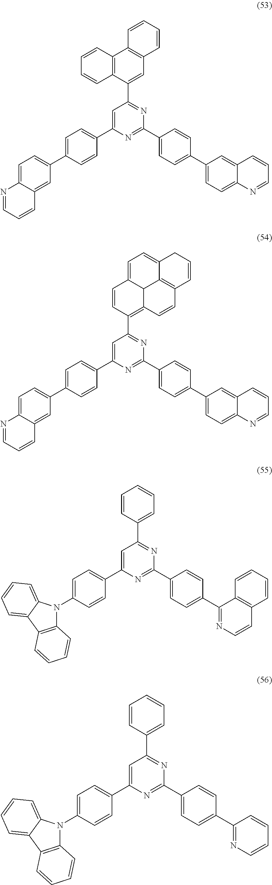


Applications Claiming Priority (5)
| Application Number | Priority Date | Filing Date | Title |
|---|---|---|---|
| KR10-2008-0082905 | 2008-08-25 | ||
| KR20080082905 | 2008-08-25 | ||
| KR10-2009-0050580 | 2009-06-08 | ||
| KR1020090050580A KR101174090B1 (en) | 2008-08-25 | 2009-06-08 | Material for organic photoelectric device and organic photoelectric device including the same |
| PCT/KR2009/004730 WO2010024572A2 (en) | 2008-08-25 | 2009-08-25 | Material for organic photoelectric device and organic photoelectric device including the same |
Related Parent Applications (1)
| Application Number | Title | Priority Date | Filing Date |
|---|---|---|---|
| PCT/KR2009/004730 Continuation WO2010024572A2 (en) | 2008-08-25 | 2009-08-25 | Material for organic photoelectric device and organic photoelectric device including the same |
Publications (2)
| Publication Number | Publication Date |
|---|---|
| US20110156014A1 US20110156014A1 (en) | 2011-06-30 |
| US8470454B2 true US8470454B2 (en) | 2013-06-25 |
Family
ID=42176272
Family Applications (1)
| Application Number | Title | Priority Date | Filing Date |
|---|---|---|---|
| US13/033,842 Active US8470454B2 (en) | 2008-08-25 | 2011-02-24 | Material for organic photoelectric device and organic photoelectric device including the same |
Country Status (7)
| Country | Link |
|---|---|
| US (1) | US8470454B2 (en) |
| EP (1) | EP2315753B1 (en) |
| JP (1) | JP5596687B2 (en) |
| KR (1) | KR101174090B1 (en) |
| CN (1) | CN102089288B (en) |
| TW (1) | TWI423961B (en) |
| WO (1) | WO2010024572A2 (en) |
Cited By (4)
| Publication number | Priority date | Publication date | Assignee | Title |
|---|---|---|---|---|
| US20110248257A1 (en) * | 2008-12-24 | 2011-10-13 | Nam-Soo Kim | Compound for an organic photoelectric device, organic photoelectric device, and display device including the same |
| US10326079B2 (en) | 2015-04-27 | 2019-06-18 | Hodogaya Chemical Co., Ltd. | Organic electroluminescent device |
| WO2020080341A1 (en) | 2018-10-17 | 2020-04-23 | 保土谷化学工業株式会社 | Compound having pyrimidine ring structure and organic electroluminescent element |
| US20200227654A1 (en) * | 2019-12-26 | 2020-07-16 | Xiamen Tianma Micro-Electronics Co., Ltd. | Organic compound, display panel and display apparatus |
Families Citing this family (27)
| Publication number | Priority date | Publication date | Assignee | Title |
|---|---|---|---|---|
| US8124762B2 (en) * | 2008-09-05 | 2012-02-28 | Korea Institute Of Science & Technology | Diphenyl amine derivatives having luminescence property |
| KR101387738B1 (en) | 2009-12-29 | 2014-04-22 | 제일모직주식회사 | Compound for organic photoelectric device and organic photoelectric device including the same |
| US9853220B2 (en) | 2011-09-12 | 2017-12-26 | Nitto Denko Corporation | Efficient organic light-emitting diodes and fabrication of the same |
| WO2013077362A1 (en) | 2011-11-22 | 2013-05-30 | 出光興産株式会社 | Aromatic heterocyclic derivative, material for organic electroluminescent element, and organic electroluminescent element |
| CN103380508B (en) | 2011-11-22 | 2017-09-08 | 出光兴产株式会社 | Aromatic heterocyclic derivative, material for organic electroluminescent element, and organic electroluminescent element |
| KR101944917B1 (en) | 2012-02-08 | 2019-02-08 | 삼성디스플레이 주식회사 | Heterocyclic compound and organic light-emitting diode including the same |
| CN103304487A (en) * | 2012-03-15 | 2013-09-18 | 海洋王照明科技股份有限公司 | Organic semiconductor material containing pyrimidine, preparation method thereof and organic light-emitting device |
| KR102025834B1 (en) | 2012-06-29 | 2019-09-27 | 삼성디스플레이 주식회사 | Novel organic emitting compound, and organic light emitting diode comprising the same |
| KR102116494B1 (en) | 2013-04-25 | 2020-05-29 | 삼성디스플레이 주식회사 | Organic light emitting diode |
| JP6301919B2 (en) * | 2013-05-20 | 2018-03-28 | 保土谷化学工業株式会社 | Novel pyrimidine derivatives and organic electroluminescence devices |
| KR102117611B1 (en) | 2013-06-12 | 2020-06-02 | 삼성디스플레이 주식회사 | Organic light emitting device |
| KR101499356B1 (en) | 2013-06-28 | 2015-03-05 | 주식회사 엘지화학 | Hetero-cyclic compound and organic light emitting device comprising the same |
| CN105473569B (en) | 2013-11-13 | 2021-01-01 | 出光兴产株式会社 | Compounds, materials for organic electroluminescence elements, organic electroluminescence elements, and electronic equipment |
| KR102235598B1 (en) * | 2014-03-11 | 2021-04-05 | 삼성디스플레이 주식회사 | Condensed cyclic compound and organic light-emitting diode comprising the same |
| KR102251735B1 (en) | 2014-04-14 | 2021-05-13 | 삼성디스플레이 주식회사 | Material for organic light emitting device, organic light emitting device, and display device including the same |
| US20170186967A1 (en) * | 2014-06-11 | 2017-06-29 | Hodogaya Chemical Co., Ltd. | Pyrimidine derivative and an organic electroluminescent device |
| KR102304716B1 (en) | 2014-06-13 | 2021-09-27 | 삼성디스플레이 주식회사 | Amine-based compounds and organic light-emitting device including the same |
| WO2016084962A1 (en) | 2014-11-28 | 2016-06-02 | 出光興産株式会社 | Compound, organic electroluminescence element material, organic electroluminescence element and electronic device |
| US10566543B2 (en) * | 2015-01-20 | 2020-02-18 | Hodogaya Chemical Co., Ltd. | Pyrimidine derivative and organic electroluminescent devices |
| US10797244B2 (en) | 2015-04-28 | 2020-10-06 | Idemitsu Kosan Co., Ltd. | Compound, material for organic electroluminescent element, organic electroluminescent element, and electronic device |
| KR20160131561A (en) | 2015-05-08 | 2016-11-16 | 주식회사 지켐 | Compound for organic photoelectric device, Organic photoelectric device including the same, and Display device including the organic photoelectric device |
| US10651392B2 (en) | 2015-09-30 | 2020-05-12 | Samsung Electronics Co., Ltd. | Organic light-emitting device |
| CN108352454B (en) * | 2015-10-29 | 2020-02-28 | 保土谷化学工业株式会社 | Organic electroluminescent device |
| EP3404735B1 (en) * | 2016-01-14 | 2023-05-10 | Hodogaya Chemical Co., Ltd. | Organic electroluminescent device |
| US20200335703A1 (en) * | 2017-11-16 | 2020-10-22 | Hodogaya Chemical Co., Ltd. | Organic electroluminescence device |
| CN111909132A (en) * | 2019-05-07 | 2020-11-10 | 北京鼎材科技有限公司 | Organic material and organic electroluminescent device using same |
| KR102381634B1 (en) * | 2019-07-05 | 2022-04-01 | 주식회사 엘지화학 | Compound and organic light emitting device comprising the same |
Citations (8)
| Publication number | Priority date | Publication date | Assignee | Title |
|---|---|---|---|---|
| EP0926216A1 (en) * | 1997-12-01 | 1999-06-30 | Chisso Corporation | Organic electroluminescent device using a triarylamine derivative |
| JP2004031004A (en) | 2002-06-24 | 2004-01-29 | Konica Minolta Holdings Inc | Organic electroluminescent element and display device |
| US20040086745A1 (en) | 2002-03-22 | 2004-05-06 | Idemitsu Kosan Co., Ltd. | Material for organic electroluminescence devices and organic electroluminescence device using the material |
| EP1424381A2 (en) | 2002-11-26 | 2004-06-02 | Konica Minolta Holdings, Inc. | Organic electroluminescent element, and display and illuminator |
| US20040110031A1 (en) | 2002-11-26 | 2004-06-10 | Mitsuhiro Fukuda | Organic electroluminescent element and display |
| US20040124766A1 (en) * | 2002-10-24 | 2004-07-01 | Satoshi Nakagawa | Organic electroluminescent device |
| WO2005105950A1 (en) | 2004-04-29 | 2005-11-10 | Ciba Specialty Chemicals Holding Inc. | Electroluminescent device |
| EP1724323A1 (en) | 2004-03-08 | 2006-11-22 | Idemitsu Kosan Co., Ltd. | Material for organic electroluminescence device and organic electroluminescence device utilizing the same |
Family Cites Families (3)
| Publication number | Priority date | Publication date | Assignee | Title |
|---|---|---|---|---|
| JP5082230B2 (en) * | 2004-12-10 | 2012-11-28 | パイオニア株式会社 | Organic compounds, charge transport materials, and organic electroluminescent devices |
| EP2246370B1 (en) * | 2008-02-22 | 2017-04-12 | Samsung Electronics Co., Ltd. | Polymer compound and organic electroluminescent device using the same |
| JP2010013421A (en) * | 2008-07-07 | 2010-01-21 | Chemiprokasei Kaisha Ltd | New bis(dicarbazolylphenyl) derivative, host material using the same and organic electroluminescencent device |
-
2009
- 2009-06-08 KR KR1020090050580A patent/KR101174090B1/en active Active
- 2009-08-25 EP EP09810177.7A patent/EP2315753B1/en active Active
- 2009-08-25 JP JP2011524896A patent/JP5596687B2/en active Active
- 2009-08-25 WO PCT/KR2009/004730 patent/WO2010024572A2/en not_active Ceased
- 2009-08-25 CN CN200980126983.0A patent/CN102089288B/en active Active
- 2009-08-25 TW TW098128520A patent/TWI423961B/en active
-
2011
- 2011-02-24 US US13/033,842 patent/US8470454B2/en active Active
Patent Citations (13)
| Publication number | Priority date | Publication date | Assignee | Title |
|---|---|---|---|---|
| EP0926216A1 (en) * | 1997-12-01 | 1999-06-30 | Chisso Corporation | Organic electroluminescent device using a triarylamine derivative |
| US20040086745A1 (en) | 2002-03-22 | 2004-05-06 | Idemitsu Kosan Co., Ltd. | Material for organic electroluminescence devices and organic electroluminescence device using the material |
| JP2004031004A (en) | 2002-06-24 | 2004-01-29 | Konica Minolta Holdings Inc | Organic electroluminescent element and display device |
| US20040124766A1 (en) * | 2002-10-24 | 2004-07-01 | Satoshi Nakagawa | Organic electroluminescent device |
| EP1424381A2 (en) | 2002-11-26 | 2004-06-02 | Konica Minolta Holdings, Inc. | Organic electroluminescent element, and display and illuminator |
| US20040110031A1 (en) | 2002-11-26 | 2004-06-10 | Mitsuhiro Fukuda | Organic electroluminescent element and display |
| US7629060B2 (en) | 2002-11-26 | 2009-12-08 | Konica Minolta Holdings, Inc. | Organic electroluminescent element, and display and illuminator |
| US20070190355A1 (en) * | 2004-03-08 | 2007-08-16 | Idemitsu Kosan Co., Ltd | Material for organic electroluminescence device and organic electroluminescence device utilizing the same |
| EP1724323A1 (en) | 2004-03-08 | 2006-11-22 | Idemitsu Kosan Co., Ltd. | Material for organic electroluminescence device and organic electroluminescence device utilizing the same |
| CN1934213A (en) | 2004-03-08 | 2007-03-21 | 出光兴产株式会社 | Material for organic electroluminescent device and organic electroluminescent device using same |
| WO2005105950A1 (en) | 2004-04-29 | 2005-11-10 | Ciba Specialty Chemicals Holding Inc. | Electroluminescent device |
| US20080199726A1 (en) | 2004-04-29 | 2008-08-21 | Ciba Specialty Chemicals Holding Inc. | Electroluminescent Device |
| CN1950479A (en) | 2004-04-29 | 2007-04-18 | 西巴特殊化学品控股有限公司 | Electroluminescent device |
Non-Patent Citations (6)
| Title |
|---|
| Baldo, et al.; Very high-efficiency green organic light-emitting devices based on electrophosphorescence; Jul. 5, 1999; pp. 4-6; vol. 75; No. 1; American Institute of Physics; United States. |
| Chinese Search Report in CN 2009801269830.0, dated Nov. 29, 2012 (Kim, et al.). |
| English language machine translation of JP 2004/031004 A, 2004. * |
| European Search Report in EP 09810177.7-1235/2315753, dated Aug. 10, 2012 (Kim, et al.). |
| O'Brien, et al.; Improved energy transfer in electrophosphorescent devices; Applied Physics Letters; Jan. 18, 1999; pp. 442-444; vol. 74; No. 3; American Institute of Physics; United States. |
| Tang, et al.; Organic electroluminescent diodes; Applied Physics Letters; Sep. 21, 1987; pp. 913-915; vol. 51; Issue 12; American Institute of Physics; United States. |
Cited By (7)
| Publication number | Priority date | Publication date | Assignee | Title |
|---|---|---|---|---|
| US20110248257A1 (en) * | 2008-12-24 | 2011-10-13 | Nam-Soo Kim | Compound for an organic photoelectric device, organic photoelectric device, and display device including the same |
| US9199966B2 (en) * | 2008-12-24 | 2015-12-01 | Cheil Industries, Inc. | Compound for an organic photoelectric device, organic photoelectric device, and display device including the same |
| US10326079B2 (en) | 2015-04-27 | 2019-06-18 | Hodogaya Chemical Co., Ltd. | Organic electroluminescent device |
| WO2020080341A1 (en) | 2018-10-17 | 2020-04-23 | 保土谷化学工業株式会社 | Compound having pyrimidine ring structure and organic electroluminescent element |
| KR20210079267A (en) | 2018-10-17 | 2021-06-29 | 호도가야 가가쿠 고교 가부시키가이샤 | A compound having a pyrimidine ring structure and an organic electroluminescent device |
| US20200227654A1 (en) * | 2019-12-26 | 2020-07-16 | Xiamen Tianma Micro-Electronics Co., Ltd. | Organic compound, display panel and display apparatus |
| US11751475B2 (en) * | 2019-12-26 | 2023-09-05 | Xiamen Tianma Micro-Electronics Co., Ltd. | Organic compound, display panel and display apparatus |
Also Published As
| Publication number | Publication date |
|---|---|
| EP2315753B1 (en) | 2015-10-07 |
| JP5596687B2 (en) | 2014-09-24 |
| EP2315753A4 (en) | 2012-09-12 |
| TW201016680A (en) | 2010-05-01 |
| US20110156014A1 (en) | 2011-06-30 |
| EP2315753A2 (en) | 2011-05-04 |
| KR20100024340A (en) | 2010-03-05 |
| KR101174090B1 (en) | 2012-08-14 |
| JP2012501091A (en) | 2012-01-12 |
| CN102089288B (en) | 2015-05-27 |
| TWI423961B (en) | 2014-01-21 |
| CN102089288A (en) | 2011-06-08 |
| WO2010024572A3 (en) | 2010-07-01 |
| WO2010024572A2 (en) | 2010-03-04 |
Similar Documents
| Publication | Publication Date | Title |
|---|---|---|
| US8470454B2 (en) | Material for organic photoelectric device and organic photoelectric device including the same | |
| US9199966B2 (en) | Compound for an organic photoelectric device, organic photoelectric device, and display device including the same | |
| US9136481B2 (en) | Compound for an organic photoelectric device, organic photoelectric device including the same, and display device including the organic photoelectric device | |
| US9012039B2 (en) | Compound for organic photoelectric device and organic photoelectric device including the same | |
| US9543530B2 (en) | Compound for organic optoelectronic device, organic light emitting diode including the same and display including the organic light emitting diode | |
| US12378207B2 (en) | Heterocyclic compound and organic electroluminescent device comprising same | |
| US8796917B2 (en) | Compound for an organic optoelectronic device, organic light emitting diode including the same, and display including the organic light emitting diode | |
| US8530063B2 (en) | Compound for organic photoelectric device and organic photoelectric device including the same | |
| US9559309B2 (en) | Compound for organic optoelectronic device, organic light emitting diode including the same, and display device including the organic light emitting diode | |
| US9419230B2 (en) | Compound for organic optoelectronic device, organic light emitting diode including the same, and display device including the organic light emitting diode | |
| US9450193B2 (en) | Compound for organic photoelectric device and organic photoelectric device including the same | |
| US8697257B2 (en) | Compound for organic photoelectric device, organic photoelectric device including the same, and display device including the organic photoelectric device | |
| US11482677B2 (en) | Compound and organic electronic device comprising same | |
| US9299935B2 (en) | Nitrogen-containing heterocyclic compounds and organic electronic device comprising the same | |
| US20120104941A1 (en) | Compound for an organic photoelectric device and organic photoelectric device including the same | |
| US20130200356A1 (en) | Compound for organic optoelectronic device, organic light emitting diode including the same and display including the organic light emitting diode | |
| US9444054B2 (en) | Compound for organic optoelectronic device and organic light emitting diode including the same | |
| US20120273771A1 (en) | Compound for organic photoelectric device and organic photoelectric device including the same | |
| US20170229659A1 (en) | Compounds and organic electronic device using the same | |
| US20150218163A1 (en) | Nitrogen-containing heterocyclic compounds and organic electronic device comprising the same | |
| US9825242B2 (en) | Compound for organic optoelectric device, organic light-emitting diode including same, display device including organic light-emitting diode | |
| US20250154085A1 (en) | Organic Compound And Organic Light-Emitting Device Comprising Same |
Legal Events
| Date | Code | Title | Description |
|---|---|---|---|
| AS | Assignment |
Owner name: CHEIL INDUSTRIES, INC., KOREA, REPUBLIC OF Free format text: ASSIGNMENT OF ASSIGNORS INTEREST;ASSIGNORS:KIM, NAM-SOO;KANG, MYEONG-SOON;JUNG, HO-KUK;AND OTHERS;SIGNING DATES FROM 20110214 TO 20110217;REEL/FRAME:025901/0854 |
|
| STCF | Information on status: patent grant |
Free format text: PATENTED CASE |
|
| FPAY | Fee payment |
Year of fee payment: 4 |
|
| MAFP | Maintenance fee payment |
Free format text: PAYMENT OF MAINTENANCE FEE, 8TH YEAR, LARGE ENTITY (ORIGINAL EVENT CODE: M1552); ENTITY STATUS OF PATENT OWNER: LARGE ENTITY Year of fee payment: 8 |
|
| MAFP | Maintenance fee payment |
Free format text: PAYMENT OF MAINTENANCE FEE, 12TH YEAR, LARGE ENTITY (ORIGINAL EVENT CODE: M1553); ENTITY STATUS OF PATENT OWNER: LARGE ENTITY Year of fee payment: 12 |