US8453318B2 - Method for making a planar coil - Google Patents

Method for making a planar coil Download PDF

Info

Publication number
US8453318B2
US8453318B2 US13/651,771 US201213651771A US8453318B2 US 8453318 B2 US8453318 B2 US 8453318B2 US 201213651771 A US201213651771 A US 201213651771A US 8453318 B2 US8453318 B2 US 8453318B2
Authority
US
United States
Prior art keywords
trench
layer
substrate
seed layer
conductive material
Prior art date
Legal status (The legal status is an assumption and is not a legal conclusion. Google has not performed a legal analysis and makes no representation as to the accuracy of the status listed.)
Expired - Fee Related
Application number
US13/651,771
Other versions
US20130043136A1 (en
Inventor
Hung Yi LIN
Ming Fa Chen
Current Assignee (The listed assignees may be inaccurate. Google has not performed a legal analysis and makes no representation or warranty as to the accuracy of the list.)
GREDMAN TAIWAN Ltd
GREDMANN TAIWAN Ltd
Original Assignee
Touch Micro System Technology Inc
Priority date (The priority date is an assumption and is not a legal conclusion. Google has not performed a legal analysis and makes no representation as to the accuracy of the date listed.)
Filing date
Publication date
Application filed by Touch Micro System Technology Inc filed Critical Touch Micro System Technology Inc
Priority to US13/651,771 priority Critical patent/US8453318B2/en
Publication of US20130043136A1 publication Critical patent/US20130043136A1/en
Application granted granted Critical
Publication of US8453318B2 publication Critical patent/US8453318B2/en
Assigned to GREDMAN TAIWAN LTD. reassignment GREDMAN TAIWAN LTD. ASSIGNMENT OF ASSIGNORS INTEREST (SEE DOCUMENT FOR DETAILS). Assignors: TOUCH MICRO-SYSTEM TECHNOLOGY CORP.
Assigned to GREDMANN TAIWAN LTD. reassignment GREDMANN TAIWAN LTD. ASSIGNMENT OF ASSIGNORS INTEREST (SEE DOCUMENT FOR DETAILS). Assignors: TOUCH MICRO-SYSTEM TECHNOLOGY CORP.
Expired - Fee Related legal-status Critical Current
Anticipated expiration legal-status Critical

Links

Images

Classifications

    • HELECTRICITY
    • H01ELECTRIC ELEMENTS
    • H01FMAGNETS; INDUCTANCES; TRANSFORMERS; SELECTION OF MATERIALS FOR THEIR MAGNETIC PROPERTIES
    • H01F41/00Apparatus or processes specially adapted for manufacturing or assembling magnets, inductances or transformers; Apparatus or processes specially adapted for manufacturing materials characterised by their magnetic properties
    • H01F41/02Apparatus or processes specially adapted for manufacturing or assembling magnets, inductances or transformers; Apparatus or processes specially adapted for manufacturing materials characterised by their magnetic properties for manufacturing cores, coils, or magnets
    • H01F41/04Apparatus or processes specially adapted for manufacturing or assembling magnets, inductances or transformers; Apparatus or processes specially adapted for manufacturing materials characterised by their magnetic properties for manufacturing cores, coils, or magnets for manufacturing coils
    • H01F41/041Printed circuit coils
    • H01F41/042Printed circuit coils by thin film techniques
    • HELECTRICITY
    • H01ELECTRIC ELEMENTS
    • H01FMAGNETS; INDUCTANCES; TRANSFORMERS; SELECTION OF MATERIALS FOR THEIR MAGNETIC PROPERTIES
    • H01F5/00Coils
    • H01F5/003Printed circuit coils
    • HELECTRICITY
    • H01ELECTRIC ELEMENTS
    • H01LSEMICONDUCTOR DEVICES NOT COVERED BY CLASS H10
    • H01L21/00Processes or apparatus adapted for the manufacture or treatment of semiconductor or solid state devices or of parts thereof
    • H01L21/70Manufacture or treatment of devices consisting of a plurality of solid state components formed in or on a common substrate or of parts thereof; Manufacture of integrated circuit devices or of parts thereof
    • H01L21/71Manufacture of specific parts of devices defined in group H01L21/70
    • H01L21/76Making of isolation regions between components
    • YGENERAL TAGGING OF NEW TECHNOLOGICAL DEVELOPMENTS; GENERAL TAGGING OF CROSS-SECTIONAL TECHNOLOGIES SPANNING OVER SEVERAL SECTIONS OF THE IPC; TECHNICAL SUBJECTS COVERED BY FORMER USPC CROSS-REFERENCE ART COLLECTIONS [XRACs] AND DIGESTS
    • Y10TECHNICAL SUBJECTS COVERED BY FORMER USPC
    • Y10TTECHNICAL SUBJECTS COVERED BY FORMER US CLASSIFICATION
    • Y10T29/00Metal working
    • Y10T29/49Method of mechanical manufacture
    • Y10T29/49002Electrical device making
    • Y10T29/4902Electromagnet, transformer or inductor
    • Y10T29/49069Data storage inductor or core
    • YGENERAL TAGGING OF NEW TECHNOLOGICAL DEVELOPMENTS; GENERAL TAGGING OF CROSS-SECTIONAL TECHNOLOGIES SPANNING OVER SEVERAL SECTIONS OF THE IPC; TECHNICAL SUBJECTS COVERED BY FORMER USPC CROSS-REFERENCE ART COLLECTIONS [XRACs] AND DIGESTS
    • Y10TECHNICAL SUBJECTS COVERED BY FORMER USPC
    • Y10TTECHNICAL SUBJECTS COVERED BY FORMER US CLASSIFICATION
    • Y10T29/00Metal working
    • Y10T29/49Method of mechanical manufacture
    • Y10T29/49002Electrical device making
    • Y10T29/4902Electromagnet, transformer or inductor
    • Y10T29/49071Electromagnet, transformer or inductor by winding or coiling
    • YGENERAL TAGGING OF NEW TECHNOLOGICAL DEVELOPMENTS; GENERAL TAGGING OF CROSS-SECTIONAL TECHNOLOGIES SPANNING OVER SEVERAL SECTIONS OF THE IPC; TECHNICAL SUBJECTS COVERED BY FORMER USPC CROSS-REFERENCE ART COLLECTIONS [XRACs] AND DIGESTS
    • Y10TECHNICAL SUBJECTS COVERED BY FORMER USPC
    • Y10TTECHNICAL SUBJECTS COVERED BY FORMER US CLASSIFICATION
    • Y10T29/00Metal working
    • Y10T29/49Method of mechanical manufacture
    • Y10T29/49002Electrical device making
    • Y10T29/4902Electromagnet, transformer or inductor
    • Y10T29/49073Electromagnet, transformer or inductor by assembling coil and core
    • YGENERAL TAGGING OF NEW TECHNOLOGICAL DEVELOPMENTS; GENERAL TAGGING OF CROSS-SECTIONAL TECHNOLOGIES SPANNING OVER SEVERAL SECTIONS OF THE IPC; TECHNICAL SUBJECTS COVERED BY FORMER USPC CROSS-REFERENCE ART COLLECTIONS [XRACs] AND DIGESTS
    • Y10TECHNICAL SUBJECTS COVERED BY FORMER USPC
    • Y10TTECHNICAL SUBJECTS COVERED BY FORMER US CLASSIFICATION
    • Y10T29/00Metal working
    • Y10T29/49Method of mechanical manufacture
    • Y10T29/49002Electrical device making
    • Y10T29/49117Conductor or circuit manufacturing
    • Y10T29/49124On flat or curved insulated base, e.g., printed circuit, etc.
    • Y10T29/4913Assembling to base an electrical component, e.g., capacitor, etc.
    • Y10T29/49146Assembling to base an electrical component, e.g., capacitor, etc. with encapsulating, e.g., potting, etc.

Abstract

A method of making a planar coil is disclosed in the present invention. First, a substrate having a trench is provided. Then, a barrier and a seed layer are formed on the substrate in sequence. An isolative layer is used for guiding a conductive material to flow into a lower portion of the trench such that accumulation of the conductive material at opening of the trench is prevented before the lower portion of the trench is completely filled up, thereby avoiding gap formation in the trench.

Description

CROSS REFERENCE TO RELATED APPLICATIONS
The present application is a Divisional application of U.S. patent application Ser. No. 12/899,836, filed on Oct. 7, 2010, now U.S. Pat. No. 8,310,328.
FIELD OF THE INVENTION
The present invention relates to a method for making a planar coil. More particularly, the present invention relates to a method for making a planar coil by micro-electro-mechanical system (MEMS) processes.
BACKGROUND OF THE INVENTION
The technology combining micromachining and integrated circuit processes becomes mature. Thus, for many micro-electro-mechanical system (MEMS) devices, microactuators are used to provide driving force and play a key part in operation. So far, electromagnetic microactuators are the main stream because the making processes are quite simple. In general, the electromagnetic microactuators are composed of a magnet and a planar coil. The planar coil can be obtained by integrated circuit processes.
The planar coil is applied to many MEMS devices. A planar coil can be used with a permanent magnet to drive micro pumps, micro valves, micro relays or other elements. Manufacture of planar coils is very important in such a field.
Please refer to FIGS. 1(A) to 1(E). A conventional method for making a planar coil is shown. A substrate 1 is provided, as shown in FIG. 1(A). Then a number of trenches 2 are formed by reactive-ion etching, as shown in FIG. 1(B). The trench 2 has a trapezoidal cross section. A barrier 3 is formed on the substrate 1. Later, a seed layer 4 is formed on the barrier 3, as shown in FIG. 1(C). Next, copper is electroplated onto the seed layer 4 until the trench 2 is filled with copper, as shown in FIG. 1(D). Finally, the seed layer 4 on the surface of the substrate 1 is removed. Accordingly, a planar coil is formed.
An obvious defect is that the cross section of the coil is trapezoidal. Usually, gaps are formed in the coil during a cryogenic process or Bosch process while making high aspect ratios of cross section for the planar coil, causing poor electrical properties of the coil. For a planar coil having a trapezoidal cross section, aspect ratio is limited.
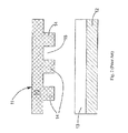
Please refer to FIG. 2 and FIG. 3. Another conventional method for making a planar coil is shown. A tooling 11 using a steel-made plate 10 is engraved with many peaks 14 and troughs 15. A hardening layer 13 is formed on a polymer substrate 12 by ultraviolet beams. Then, the hardening layer 13 is pressed by the tooling 11. Due to the peaks 14 and troughs 15, a number of high aspect ratio trenches will be formed on the hardening layer 13. Next, a seed layer 16 of copper is formed by vapor deposition process on the hardening layer 13. A coil layer 17 is electroplated onto the seed layer 16. Finally, after the redundant portion of the coil layer 17 is removed, a planar coil is formed.
The method utilizes the tooling 11 and the hardening layer 13 to provide high aspect ratio trenches for making the planar coil. No matter what additional agent is used to enhance the hardness of tooling 11, the tooling 11 will be worn out after long-term use. A designated shape of the planar coil can not be achieved. In addition, the coil layer 17 will stick to the hardening layer 13 if the hardening layer 13 is not firm enough.
From the description above, a method for making planar coils with good quality is desired. Especially, a method for making planar coils with high aspect ratio is desperately needed.
SUMMARY OF THE INVENTION
This paragraph extracts and compiles some features of the present invention; other features will be disclosed in the follow-up paragraphs. It is intended to cover various modifications and similar arrangements included within the spirit and scope of the appended claims.
In accordance with an aspect of the present invention, a method for making a planar coil, includes the steps of: a) providing a substrate; b) covering a predetermined area of the substrate with a patterned photoresist layer; c) etching the substrate to form a trench at a place outside of the predetermined area; d) removing the photoresist layer; e) applying a barrier on the substrate; f) growing a seed layer on the barrier; g) covering the predetermined area with an isolative layer which extends slightly into the trench; h) filling up the trench with a conductive material by electroplating; and i) removing a portion of the isolative layer and the seed layer located above the predetermined area. The isolative layer guides the conductive material to flow into a lower portion of the trench such that accumulation of the conductive material at opening of the trench is prevented before the lower portion of the trench is completely filled up, thereby avoiding gap formation in the trench.
Preferably, step c) is performed by deep reactive-ion etching (DRIE).
Preferably, step d) is conducted by use of acetone.
Preferably, step i) is conducted by use of buffered oxide etch (BOE) for removing the isolative layer, and hydrogen peroxide, ammonium hydroxide, or an acetic acid based etchant is used for removing the seed layer.
Preferably, the seed layer is formed by sputtering.
Preferably, the substrate is made of silicon.
Preferably, the barrier is electrically insulated.
Preferably, the barrier is made of silicon dioxide.
Preferably, the seed layer is made of copper, titanium, or a mixture thereof.
Preferably, the isolative layer is made of silicon dioxide.
Preferably, step g) is performed by plasma-enhanced chemical vapor deposition (PECVD).
Preferably, the conductive material is copper.
Preferably, the method further includes a step of j) forming a hole through center of the substrate to form a loop-shaped planar coil.
In accordance with another aspect of the present invention, a planar coil includes: a substrate having a trench formed therein; a barrier on the substrate; and a seed layer on the barrier in the trench. The trench is filled up with a conductive material and a slot is formed between the conductive material and a portion of the seed layer near the surface of the planar coil.
Preferably, the slot is filled with an isolative material.
Preferably, the isolative material comprises silicon dioxide.
Preferably, the substrate is made of silicon.
Preferably, the barrier is made of silicon dioxide.
Preferably, the seed layer is made of copper, titanium, or a mixture thereof.
Preferably, the conductive material is copper.
Preferably, the substrate has a hole through the center to form a loop-shaped planar coil.
BRIEF DESCRIPTION OF THE DRAWINGS
FIGS. 1(A) to 1(E) illustrate a prior art of making a planar coil.
FIGS. 2 and 3 illustrate another prior art of making a planar coil.
FIG. 4 is a planar coil according to an embodiment of the present invention.
FIG. 5 shows a patterned photoresist layer applied on a substrate.
FIG. 6 shows the substrate having a number of trenches formed therein.
FIG. 7 shows a barrier formed on the substrate.
FIG. 8 shows a seed layer formed on the barrier.
FIG. 9 shows an isolative layer partially applied on the substrate.
FIG. 10 shows the trenches filled up with a conductive material by electroplating.
FIG. 11 shows a completed planar coil according to the present invention.
FIG. 12 shows another planar coil according to the present invention.
DETAILED DESCRIPTION OF THE PREFERRED EMBODIMENT
Please refer to FIGS. 4 to 11. An embodiment is described. FIG. 4 is a top view of a planar coil 110. It has a coil body 105 formed on a substrate 100. In this embodiment, the substrate 100 is a silicon substrate. In order to make illustration of the present invention more comprehensive, a cross section is taken along line AA′ to depict the steps of the invention.
Please refer to FIG. 5. In the beginning of making the planar coil 110, a patterned photoresist layer 101 is applied on the substrate 100 covering a predetermined area. Later, a number of trenches 102 are formed by etching the substrate at a place outside of the predetermined area, as shown in FIG. 6. In the present invention, deep reactive-ion etching (DRIE) is used for etching. DRIE is a highly anisotropic etching process used to create deep, steep-sided holes and trenches in wafers, with aspect ratios of 20:1 or more. It was developed for micro electromechanical systems (MEMS) which require these features. There are two main technologies for high-rate DRIE: cryogenic process and Bosch process. Both Bosch and cryogenic processes can fabricate vertical walls, but often the walls are sloped at an angle. By using the DRIE, the walls of the trenches 102 can be substantially vertical. The planar coil 110 can have better electrical properties and smaller size.
Then, the patterned photoresist layer 101 is removed. Acetone can be use to wash off the patterned photoresist layer 101. Next, a barrier 103 is formed over the substrate 100, as shown in FIG. 7. The barrier 103 is formed by conducting thermal oxidation to the substrate 100. The barrier 103 is made of silicon dioxide. It provides good electrical insulation for the coil body 105. Although the barrier 103 is formed on the whole substrate 100 in this embodiment, it can be formed only on the predetermined area.
Later, please see FIG. 8. A seed layer 104 is formed on the barrier 103. In the present invention, the seed layer 104 is formed by sputtering. The seed layer 104 is made of copper. In practice, it can also be made of titanium or a mixture of copper and titanium. The seed layer 104 is used to facilitate ions in an electroplating process later on mentioned to be attached to the barrier 103.
FIG. 9 shows an isolative layer 106 formed on the seed layer 104 covering the predetermined area and extending slightly into the trenches 102. The isolative layer 106 is made of silicon dioxide. The isolative layer 106 is used as a lubricant for preventing ions from sticking thereon. Plasma-enhanced chemical vapor deposition (PECVD) is used for forming the isolative layer 106 on the seed layer 104 because PECVD can be performed under low temperature, thereby preventing the seed layer 104 from melting at high temperature.
Next, please refer to FIG. 10. The trenches 102 of the substrate 100 are filled up with a conductive material 1051 to form the coil body 105 by electroplating. In the present invention, the conductive material 1051 is copper so that the copper ions can adhere to the seed layer 104. In addition, when the copper ions reaches the isolative layer 106 (PEOX), they will easily slip into the trenches 102. In other words, the isolative layer 106 guides the conductive material 1051 to flow into a lower portion of the trench 102 such that accumulation of the conductive material 1051 at opening of the trench 102 is prevented before the lower portion of the trench 102 is completely filled up, thereby avoiding gap formation in the trench 102.
Please refer to FIG. 12. Finally, a portion of the isolative layer 106 and the seed layer 104 trenches located above the predetermined area are removed. The planar coil 110 is finished. In this step, buffered oxide etch (BOE) for removing the isolative layer, and hydrogen peroxide, ammonium hydroxide, or an acetic acid based etchant is used for removing the seed layer is used for removal.
The aforementioned process for making a planar coil can also be used for making a loop-shaped planar coil 210 by forming a hole 207 through center of a substrate 200 such that a coil body 205 is looped around the hole 207, as shown in FIG. 12.
Furthermore, the isolative layer 106 between the conductive material 1051 and the seed layer 104 can also be removed while the isolative layer 106 located above the predetermined area is removed. A slot (not shown) may be formed between the conductive material 1051 and a portion of the seed layer 104 near the surface of the planar coil 110.
By the present invention, additives are not needed in the conductive material for reducing deposition on the surface of the planar coil which may cause high resistance. Moreover, since the isolative layer 106 guides the conductive material 1051 to flow into a lower portion of the trench 102 such that accumulation of the conductive material 1051 at opening of the trench 102 is prevented before the lower portion of the trench 102 is completely filled up, the conductive material 1051 is unlikely to overflow from the trench 102, and therefore, a flattening process such as chemical mechanical polishing (CMP) process is not needed.
While the invention has been described in terms of what is presently considered to be the most practical and preferred embodiment, it is to be understood that the invention needs not be limited to the disclosed embodiment. On the contrary, it is intended to cover various modifications and similar arrangements included within the spirit and scope of the appended claims, which are to be accorded with the broadest interpretation so as to encompass all such modifications and similar structures.

Claims (13)

What is claimed is:
1. A method for making a planar coil, comprising the steps of:
a) providing a substrate;
b) covering a predetermined area of the substrate with a patterned photoresist layer;
c) etching the substrate to form a trench at a place outside of the predetermined area;
d) removing the photoresist layer;
e) applying a barrier on the substrate;
f) growing a seed layer on the barrier;
g) covering the predetermined area with an isolative layer which extends slightly into the trench;
h) filling up the trench with a conductive material by electroplating; and
i) removing a portion of the isolative layer and the seed layer located above the predetermined area;
wherein the isolative layer guides the conductive material to flow into a lower portion of the trench such that accumulation of the conductive material at opening of the trench is prevented before the lower portion of the trench is completely filled up, thereby avoiding gap formation in the trench.
2. The method according to claim 1, wherein step c) is performed by deep reactive-ion etching (DRIE).
3. The method according to claim 1, wherein step d) is conducted by use of acetone.
4. The method according to claim 1, wherein step i) is conducted by use of buffered oxide etch (BOE) for removing the isolative layer, and hydrogen peroxide, ammonium hydroxide, or an acetic acid based etchant is used for removing the seed layer.
5. The method according to claim 1, wherein the seed layer is formed by sputtering.
6. The method according to claim 1, wherein the substrate is made of silicon.
7. The method according to claim 1, wherein the barrier is electrically insulated.
8. The method according to claim 7, wherein the barrier is made of silicon dioxide.
9. The method according to claim 1, wherein the seed layer is made of copper, titanium, or a mixture thereof.
10. The method according to claim 1, wherein the isolative layer is made of silicon dioxide.
11. The method according to claim 1, wherein step g) is performed by plasma-enhanced chemical vapor deposition (PECVD).
12. The method according to claim 1, wherein the conductive material is copper.
13. The method according to claim 1, further comprising a step of j) forming a hole through center of the substrate to form a loop-shaped planar coil.
US13/651,771 2010-10-07 2012-10-15 Method for making a planar coil Expired - Fee Related US8453318B2 (en)

Priority Applications (1)

Application Number Priority Date Filing Date Title
US13/651,771 US8453318B2 (en) 2010-10-07 2012-10-15 Method for making a planar coil

Applications Claiming Priority (2)

Application Number Priority Date Filing Date Title
US12/899,836 US8310328B2 (en) 2010-10-07 2010-10-07 Planar coil and method of making the same
US13/651,771 US8453318B2 (en) 2010-10-07 2012-10-15 Method for making a planar coil

Related Parent Applications (1)

Application Number Title Priority Date Filing Date
US12/899,836 Division US8310328B2 (en) 2010-10-07 2010-10-07 Planar coil and method of making the same

Publications (2)

Publication Number Publication Date
US20130043136A1 US20130043136A1 (en) 2013-02-21
US8453318B2 true US8453318B2 (en) 2013-06-04

Family

ID=45924690

Family Applications (2)

Application Number Title Priority Date Filing Date
US12/899,836 Expired - Fee Related US8310328B2 (en) 2010-10-07 2010-10-07 Planar coil and method of making the same
US13/651,771 Expired - Fee Related US8453318B2 (en) 2010-10-07 2012-10-15 Method for making a planar coil

Family Applications Before (1)

Application Number Title Priority Date Filing Date
US12/899,836 Expired - Fee Related US8310328B2 (en) 2010-10-07 2010-10-07 Planar coil and method of making the same

Country Status (1)

Country Link
US (2) US8310328B2 (en)

Cited By (1)

* Cited by examiner, † Cited by third party
Publication number Priority date Publication date Assignee Title
CN105572610A (en) * 2015-12-23 2016-05-11 中国人民解放军国防科学技术大学 MEMS multilayer coil and preparation method thereof

Families Citing this family (3)

* Cited by examiner, † Cited by third party
Publication number Priority date Publication date Assignee Title
DE102012018013B4 (en) 2012-09-12 2014-09-18 X-Fab Semiconductor Foundries Ag Spiral, integrable coils with centered terminals in planar trench-isolated silicon semiconductor technology
CN110136911A (en) * 2018-02-02 2019-08-16 盈成科技有限公司 Loop construction and preparation method thereof
US11953567B2 (en) 2020-09-08 2024-04-09 Analog Devices International Unlimited Company Magnetic multi-turn sensor and method of manufacture

Citations (2)

* Cited by examiner, † Cited by third party
Publication number Priority date Publication date Assignee Title
US6720248B2 (en) * 2002-04-01 2004-04-13 Hynix Semiconductor Inc. Method of forming metal interconnection layer in semiconductor device
US7425506B1 (en) * 2003-01-15 2008-09-16 Novellus Systems Inc. Methods of providing an adhesion layer for adhesion of barrier and/or seed layers to dielectric films

Family Cites Families (14)

* Cited by examiner, † Cited by third party
Publication number Priority date Publication date Assignee Title
WO1999027579A1 (en) * 1997-11-26 1999-06-03 Applied Materials, Inc. Damage-free sculptured coating deposition
US6184137B1 (en) * 1998-11-25 2001-02-06 Applied Materials, Inc. Structure and method for improving low temperature copper reflow in semiconductor features
JP2002057126A (en) * 2000-08-10 2002-02-22 Fujitsu Ltd Semiconductor device and method of manufacturing the same
US7172497B2 (en) * 2001-01-05 2007-02-06 Asm Nutool, Inc. Fabrication of semiconductor interconnect structures
JP3540302B2 (en) * 2001-10-19 2004-07-07 Necエレクトロニクス株式会社 Semiconductor device and manufacturing method thereof
US7750413B2 (en) * 2003-06-16 2010-07-06 Nec Corporation Semiconductor device and method for manufacturing same
US7068139B2 (en) * 2003-09-30 2006-06-27 Agere Systems Inc. Inductor formed in an integrated circuit
JP4150689B2 (en) * 2004-03-29 2008-09-17 富士通株式会社 Multilayer wiring structure formed in a semiconductor integrated circuit device
KR100770541B1 (en) * 2005-12-29 2007-10-25 동부일렉트로닉스 주식회사 Semiconductor device and manufacturing method thereof
JP4559973B2 (en) * 2006-01-13 2010-10-13 富士通セミコンダクター株式会社 Manufacturing method of semiconductor device
US20080079530A1 (en) * 2006-10-02 2008-04-03 Weidman Timothy W Integrated magnetic features
JP2008166529A (en) * 2006-12-28 2008-07-17 Spansion Llc Semiconductor device manufacturing method
US7935640B2 (en) * 2007-08-10 2011-05-03 Tokyo Electron Limited Method for forming a damascene structure
US7943473B2 (en) * 2009-01-13 2011-05-17 Maxim Integrated Products, Inc. Minimum cost method for forming high density passive capacitors for replacement of discrete board capacitors using a minimum cost 3D wafer-to-wafer modular integration scheme

Patent Citations (2)

* Cited by examiner, † Cited by third party
Publication number Priority date Publication date Assignee Title
US6720248B2 (en) * 2002-04-01 2004-04-13 Hynix Semiconductor Inc. Method of forming metal interconnection layer in semiconductor device
US7425506B1 (en) * 2003-01-15 2008-09-16 Novellus Systems Inc. Methods of providing an adhesion layer for adhesion of barrier and/or seed layers to dielectric films

Cited By (2)

* Cited by examiner, † Cited by third party
Publication number Priority date Publication date Assignee Title
CN105572610A (en) * 2015-12-23 2016-05-11 中国人民解放军国防科学技术大学 MEMS multilayer coil and preparation method thereof
CN105572610B (en) * 2015-12-23 2018-03-20 中国人民解放军国防科学技术大学 MEMS lattice coils and preparation method thereof

Also Published As

Publication number Publication date
US20120086537A1 (en) 2012-04-12
US8310328B2 (en) 2012-11-13
US20130043136A1 (en) 2013-02-21

Similar Documents

Publication Publication Date Title
US8453318B2 (en) Method for making a planar coil
US6720201B2 (en) MEMS device and fabrication method thereof
US7622783B2 (en) MEMS thermal actuator and method of manufacture
US9173291B2 (en) Circuit board and method for manufacturing the same
CN107799483B (en) Semiconductor package structure and manufacturing method thereof
US10192672B2 (en) Coil component and method of manufacturing the same
JP2008514441A (en) Novel structure of microelectronics and microsystem, and manufacturing method thereof
US20140300249A1 (en) Mems device anchoring
WO2002103687A3 (en) Method of making a magnetic head
CN109326421B (en) MEMS (micro-electromechanical system) annular solenoid inductor and manufacturing method thereof
EP2053017A2 (en) Electrical connection through a substrate to a microelectromechanical devise
US20160064647A1 (en) Size-controllable opening and method of making same
US6809436B2 (en) Microactuator having a ferromagnetic substrate
US10332850B2 (en) Method for producing contact areas on a semiconductor substrate
US6560864B1 (en) Process for manufacturing a flat coil
TWI574911B (en) Method for mems device fabrication and device formed
EP3393966B1 (en) A method for manufacturing a hollow mems structure
US20140287202A1 (en) Transfer mold manufacturing method, transfer mold manufactured thereby, and component produced by the transfer mold
US20150028488A1 (en) Method for manufacturing a conducting contact on a conducting element
US7704868B2 (en) Fabrication of a micro-electromechanical system (MEMS) device from a complementary metal oxide semiconductor (CMOS)
CN110021553B (en) Through hole structure and method thereof
US6631546B1 (en) Self-aligned void filling for mushroomed plating
US20150151961A1 (en) Lateral etch stop for nems release etch for high density nems/cmos monolithic integration
CN110182752B (en) Method for forming fine structure by electroplating, fine structure and electronic device
CN116941008A (en) Micro-electromechanical system switch and manufacturing method thereof

Legal Events

Date Code Title Description
AS Assignment

Owner name: GREDMAN TAIWAN LTD., TAIWAN

Free format text: ASSIGNMENT OF ASSIGNORS INTEREST;ASSIGNOR:TOUCH MICRO-SYSTEM TECHNOLOGY CORP.;REEL/FRAME:032978/0275

Effective date: 20140414

AS Assignment

Owner name: GREDMANN TAIWAN LTD., TAIWAN

Free format text: ASSIGNMENT OF ASSIGNORS INTEREST;ASSIGNOR:TOUCH MICRO-SYSTEM TECHNOLOGY CORP.;REEL/FRAME:033009/0642

Effective date: 20140414

REMI Maintenance fee reminder mailed
LAPS Lapse for failure to pay maintenance fees
STCH Information on status: patent discontinuation

Free format text: PATENT EXPIRED DUE TO NONPAYMENT OF MAINTENANCE FEES UNDER 37 CFR 1.362

FP Lapsed due to failure to pay maintenance fee

Effective date: 20170604