US8436398B2 - Back diffusion suppression structures - Google Patents
Back diffusion suppression structures Download PDFInfo
- Publication number
- US8436398B2 US8436398B2 US12/756,088 US75608810A US8436398B2 US 8436398 B2 US8436398 B2 US 8436398B2 US 75608810 A US75608810 A US 75608810A US 8436398 B2 US8436398 B2 US 8436398B2
- Authority
- US
- United States
- Prior art keywords
- layer
- region
- transistor
- barrier layer
- iii nitride
- Prior art date
- Legal status (The legal status is an assumption and is not a legal conclusion. Google has not performed a legal analysis and makes no representation as to the accuracy of the status listed.)
- Active, expires
Links
Images


Classifications
-
- H—ELECTRICITY
- H10—SEMICONDUCTOR DEVICES; ELECTRIC SOLID-STATE DEVICES NOT OTHERWISE PROVIDED FOR
- H10D—INORGANIC ELECTRIC SEMICONDUCTOR DEVICES
- H10D30/00—Field-effect transistors [FET]
- H10D30/40—FETs having zero-dimensional [0D], one-dimensional [1D] or two-dimensional [2D] charge carrier gas channels
- H10D30/47—FETs having zero-dimensional [0D], one-dimensional [1D] or two-dimensional [2D] charge carrier gas channels having two-dimensional [2D] charge carrier gas channels, e.g. nanoribbon FETs or high electron mobility transistors [HEMT]
- H10D30/471—High electron mobility transistors [HEMT] or high hole mobility transistors [HHMT]
- H10D30/475—High electron mobility transistors [HEMT] or high hole mobility transistors [HHMT] having wider bandgap layer formed on top of lower bandgap active layer, e.g. undoped barrier HEMTs such as i-AlGaN/GaN HEMTs
-
- H—ELECTRICITY
- H10—SEMICONDUCTOR DEVICES; ELECTRIC SOLID-STATE DEVICES NOT OTHERWISE PROVIDED FOR
- H10D—INORGANIC ELECTRIC SEMICONDUCTOR DEVICES
- H10D30/00—Field-effect transistors [FET]
- H10D30/01—Manufacture or treatment
- H10D30/015—Manufacture or treatment of FETs having heterojunction interface channels or heterojunction gate electrodes, e.g. HEMT
-
- H—ELECTRICITY
- H10—SEMICONDUCTOR DEVICES; ELECTRIC SOLID-STATE DEVICES NOT OTHERWISE PROVIDED FOR
- H10D—INORGANIC ELECTRIC SEMICONDUCTOR DEVICES
- H10D30/00—Field-effect transistors [FET]
- H10D30/60—Insulated-gate field-effect transistors [IGFET]
- H10D30/67—Thin-film transistors [TFT]
- H10D30/6729—Thin-film transistors [TFT] characterised by the electrodes
- H10D30/6737—Thin-film transistors [TFT] characterised by the electrodes characterised by the electrode materials
- H10D30/6738—Schottky barrier electrodes
-
- H—ELECTRICITY
- H10—SEMICONDUCTOR DEVICES; ELECTRIC SOLID-STATE DEVICES NOT OTHERWISE PROVIDED FOR
- H10D—INORGANIC ELECTRIC SEMICONDUCTOR DEVICES
- H10D30/00—Field-effect transistors [FET]
- H10D30/60—Insulated-gate field-effect transistors [IGFET]
- H10D30/67—Thin-film transistors [TFT]
- H10D30/674—Thin-film transistors [TFT] characterised by the active materials
- H10D30/675—Group III-V materials, Group II-VI materials, Group IV-VI materials, selenium or tellurium
-
- H—ELECTRICITY
- H10—SEMICONDUCTOR DEVICES; ELECTRIC SOLID-STATE DEVICES NOT OTHERWISE PROVIDED FOR
- H10D—INORGANIC ELECTRIC SEMICONDUCTOR DEVICES
- H10D62/00—Semiconductor bodies, or regions thereof, of devices having potential barriers
- H10D62/10—Shapes, relative sizes or dispositions of the regions of the semiconductor bodies; Shapes of the semiconductor bodies
- H10D62/17—Semiconductor regions connected to electrodes not carrying current to be rectified, amplified or switched, e.g. channel regions
- H10D62/343—Gate regions of field-effect devices having PN junction gates
-
- H—ELECTRICITY
- H10—SEMICONDUCTOR DEVICES; ELECTRIC SOLID-STATE DEVICES NOT OTHERWISE PROVIDED FOR
- H10D—INORGANIC ELECTRIC SEMICONDUCTOR DEVICES
- H10D62/00—Semiconductor bodies, or regions thereof, of devices having potential barriers
- H10D62/80—Semiconductor bodies, or regions thereof, of devices having potential barriers characterised by the materials
- H10D62/85—Semiconductor bodies, or regions thereof, of devices having potential barriers characterised by the materials being Group III-V materials, e.g. GaAs
-
- H—ELECTRICITY
- H10—SEMICONDUCTOR DEVICES; ELECTRIC SOLID-STATE DEVICES NOT OTHERWISE PROVIDED FOR
- H10D—INORGANIC ELECTRIC SEMICONDUCTOR DEVICES
- H10D64/00—Electrodes of devices having potential barriers
- H10D64/60—Electrodes characterised by their materials
- H10D64/64—Electrodes comprising a Schottky barrier to a semiconductor
-
- H—ELECTRICITY
- H10—SEMICONDUCTOR DEVICES; ELECTRIC SOLID-STATE DEVICES NOT OTHERWISE PROVIDED FOR
- H10D—INORGANIC ELECTRIC SEMICONDUCTOR DEVICES
- H10D62/00—Semiconductor bodies, or regions thereof, of devices having potential barriers
- H10D62/80—Semiconductor bodies, or regions thereof, of devices having potential barriers characterised by the materials
- H10D62/85—Semiconductor bodies, or regions thereof, of devices having potential barriers characterised by the materials being Group III-V materials, e.g. GaAs
- H10D62/8503—Nitride Group III-V materials, e.g. AlN or GaN
Definitions
- the present invention relates to the field of enhancement mode gallium nitride (GaN) transistors. More particularly, the invention relates to an enhancement mode GaN transistor with a diffusion barrier.
- GaN gallium nitride
- Gallium nitride (GaN) semiconductor devices are increasingly desirable for power semiconductor devices because of their ability to carry large current and support high voltages. Development of these devices has generally been aimed at high power/high frequency applications. Devices fabricated for these types of applications are based on general device structures that exhibit high electron mobility and are referred to variously as heterojunction field effect transistors (HFET), high electron mobility transistors (HEMT), or modulation doped field effect transistors (MODFET). These types of devices can typically withstand high voltages, e.g., 100 Volts, while operating at high frequencies, e.g., 100 kHz-10 GHz.
- HFET heterojunction field effect transistors
- HEMT high electron mobility transistors
- MODFET modulation doped field effect transistors
- a GaN HEMT device includes a nitride semiconductor with at least two nitride layers. Different materials formed on the semiconductor or on a buffer layer causes the layers to have different band gaps. The different material in the adjacent nitride layers also causes polarization, which contributes to a conductive two dimensional electron gas (2DEG) region near the junction of the two layers, specifically in the layer with the narrower band gap.
- 2DEG conductive two dimensional electron gas
- the nitride layers that cause polarization typically include a barrier layer of AlGaN adjacent to a layer of GaN to include the 2DEG, which allows charge to flow through the device. This barrier layer may be doped or undoped. Because the 2DEG region exists under the gate at zero gate bias, most nitride devices are normally on, or depletion mode devices. If the 2DEG region is depleted, i.e. removed, below the gate at zero applied gate bias, the device can be an enhancement mode device. Enhancement mode devices are normally off and are desirable because of the added safety they provide and because they are easier to control with simple, low cost drive circuits. An enhancement mode device requires a positive bias applied at the gate in order to conduct current.
- FIG. 1 illustrates a conventional enhancement mode GaN transistor device 100 without a diffusion barrier.
- Device 100 includes substrate 101 that can be composed of silicon (Si), silicon carbide (SiC), sapphire, or other material, transition layers 102 typically composed of AlN and AlGaN that is about 0.1 to about 1.0 ⁇ m in thickness, buffer material 103 typically composed of GaN that is about 0.5 to about 10 ⁇ m in thickness, barrier material 104 typically composed of AlGaN where the Al to Ga ratio is about 0.1 to about 0.5 with thickness from about 0.005 to about 0.03 ⁇ m, p-type AlGaN 105 , heavily doped p-type GaN 106 , isolation region 107 , passivation region 108 , ohmic contact metals 109 and 110 for the source and drain, typically composed of Ti and Al with a capping metal such as Ni and Au, and gate metal 111 typically composed of a nickel (Ni) and gold (Au) metal contact over a p-type GaN gate.
- a second disadvantage of the conventional GaN transistor is the high gate leakage when the transistor is turned on by applying positive voltage to the gate contact.
- Mg atoms diffuse to the growth surface. When growth is terminated, a heavily doped layer exists at the surface. When positive bias is applied to the gate contact, a large current is generated due to the high doping at the top of this layer.
- FIG. 1 illustrates a cross-sectional view of a conventional enhancement mode GaN transistor device.
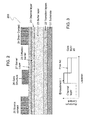
- FIG. 2 illustrates a cross-sectional view of an enhancement mode GaN transistor device formed according to a first embodiment of the present invention.
- FIG. 3 is a schematic representation comparing the aluminum content in conventional GaN transistors and the device of FIG. 2 .
- FIG. 4 illustrates a cross-sectional view of an enhancement mode GaN transistor device formed according to a second embodiment of the present invention.
- FIG. 5 is a schematic representation comparing the aluminum content in conventional GaN transistors and the device of FIG. 4 .
- FIG. 6 illustrates a cross-sectional view of an enhancement mode GaN transistor device formed according to a third embodiment of the present invention.
- FIG. 7 is a schematic representation comparing the aluminum content in conventional GaN transistors and the device of FIG. 6 .
- FIG. 8 illustrates a cross-sectional view of an enhancement mode GaN transistor device formed according to a fourth embodiment of the present invention.
- FIG. 9 is a schematic representation comparing the magnesium content in conventional GaN transistors and the device of FIG. 8 .
- FIG. 10 illustrates a cross-sectional view of an enhancement mode GaN transistor device formed according to a fifth embodiment of the present invention.
- FIG. 11 is a schematic representation comparing the magnesium content in conventional GaN transistors and the device of FIG. 10 .
- FIG. 12 illustrates a cross-sectional view of an enhancement mode GaN transistor device formed according to a sixth embodiment of the present invention.
- FIG. 13 is a schematic representation comparing the magnesium content in conventional GaN transistors and the device of FIG. 12 .
- FIG. 14 illustrates a cross-sectional view of an enhancement mode GaN transistor device formed according to a seventh embodiment of the present invention.
- FIGS. 15A-15D illustrate a method of forming an enhancement mode GaN transistor device according to an embodiment of the present invention.
- Embodiments of the invention described herein relate to an enhancement mode GaN transistor with a diffusion barrier that prevents Mg atoms from diffusing through the crystal into the active regions of the device.
- the embodiments are based on the addition of a diffusion barrier and/or a graded doping profile to reduce or eliminate the diffusion of dopant atoms (e.g., Mg).
- dopant atoms e.g., Mg.
- a thin AlN, or high Al content AlGaN layer is deposited above the primary channel layer to block the back diffusion of Mg into this region.
- a thin AlN or high Al AlGaN layer is deposited within or above the barrier layer.
- the Mg doping profile is controlled to reduce the quantity of Mg diffused into or through the barrier layer by adding an undoped region between the p-GaN layer and barrier layer.
- a doping modification near the gate contact is used either to facilitate ohmic or Schottky contact formation.
- FIG. 2 illustrates a cross-sectional view of the device 200 .
- Device 200 includes substrate 21 composed of Si, SiC, sapphire, or other material, transition layers 22 typically composed of AlN and AlGaN from about 0.1 to about 1.0 ⁇ m in thickness, buffer layer 23 typically composed of GaN from about 0.5 to about 10 ⁇ m in thickness, channel layer 20 typically composed of GaN or InGaN with a thickness from about 0.01 to about 0.3 ⁇ m, barrier layer 27 typically composed of AlGaN where the Al fraction is about 0.1 to about 0.5 with a thickness between about 0.005 and about 0.03 ⁇ m, gate structure 26 typically composed of p-type GaN with a refractory metal contact such as Ta, Ti, TiN, W, or WSi 2 .
- transition layers 22 typically composed of AlN and AlGaN from about 0.1 to about 1.0 ⁇ m in thickness
- buffer layer 23 typically composed of GaN from about 0.5 to about 10 ⁇ m in thickness
- channel layer 20 typically composed of Ga
- the p-type GaN and refractory metal contact are each between about 0.01 and about 1.0 ⁇ m in thickness.
- Ohmic contact metals 24 , 25 are composed of Ti and Al with a capping metal such as Ni and Au or Ti and TiN.
- Diffusion barrier 28 is typically composed of AlGaN, where the Al fraction is between about 0.2 and about 1 with a thickness between about 0.001 and about 0.003 ⁇ m. The Al fraction is the content of Al such that Al fraction plus Ga fraction equals 1.
- Buffer layer 23 , barrier layer 27 , and diffusion barrier 28 are made of a III Nitride material.
- a III Nitride material can be composed of In x Al y Ga 1-x-y N where x+y ⁇ 1.
- FIG. 2 has higher Al content close to the channel layer, and lower Al content near the gate layer.
- FIG. 3 A comparison of Al content between the channel layer and gate layer in a conventional GaN transistor and the structure of FIG. 2 is shown in FIG. 3 .
- the diffusion barrier layer 28 above the channel layer is high in Al, while the barrier layer 27 is of lower Al content.
- FIG. 3 shows 2 distinct layers of constant Al content, the combination of layer 28 and 27 into a graded Al content layer can also be employed, such that the Al content is graded from high near the channel layer to low near the gate structure.
- This grading can be done in many fashions, such as linear, multiple steps down, alternating between high and low Al content while gradually decreasing the average Al content, or alternating between high and low Al content while changing the thickness of the high and low Al layers from thicker high Al near the channel to thinner high Al near the gate.
- the high Al content material blocks diffusion of Mg and confines it to regions above the channel layer.
- the high Al content layer also leads to high electron mobility. In the structure shown in FIG. 2 , however, diffusion still proceeds into the top barrier layer.
- FIG. 4 illustrates a cross-sectional view of the device 300 .
- FIG. 4 is similar to FIG. 2 , but differs in that diffusion barrier 38 and barrier layer 37 are inverted from their positions in FIG. 2 , thus providing diffusion barrier 38 next to the gate structure 36 .
- the dimensions and compositions of the various layers are similar to that of the first embodiment.
- FIG. 5 A comparison of Al content between the channel layer and gate layer in a conventional GaN transistor and the structure of FIG. 4 is shown in FIG. 5 .
- the barrier layer 37 above the channel layer is low in Al, while the diffusion barrier layer 38 is of higher Al content.
- the high Al content material blocks diffusion of Mg and confines it to regions above the barrier layers.
- the lower Al content layer does not have the advantage of higher electron mobility possessed by the first embodiment.
- FIG. 6 illustrates a cross-sectional view of the device 400 .
- the third embodiment is essentially a combination of the first and second embodiments described above, and includes two diffusion barrier layers 48 , 49 , one of either side of the barrier layer 47 .
- the dimensions and compositions of the various layers are similar to that of the first and second embodiments.
- FIG. 6 has a triple layer of different Al contents with higher Al content close to the gate layer and higher Al content near the channel layer.
- a comparison of Al content between the buffer layer and gate layer in a conventional GaN transistor and the structure of FIG. 6 is shown in FIG. 7 .
- the diffusion layer 49 above the channel layer is high in Al, while the barrier layer 47 is of lower Al content, and the other diffusion layer 48 is again of high Al content.
- the high Al content material of layer 48 blocks diffusion of Mg, and confines it to regions above the barrier layers.
- the high Al content material of layer 49 leads to higher electron mobility.
- FIG. 8 illustrates a cross-sectional view of the device 500 .
- This embodiment is similar to the first and second embodiments described above, but has a p-type GaN gate with a Mg doping profile and does not have diffusion barrier layers.
- the gate layer 57 in this embodiment has lower Mg concentration near the barrier layer 54 and higher Mg concentration near the gate contact 58 .
- Typical values for Mg concentration in gate layer 57 are about 10 16 atoms per cm 3 near the barrier layer, increasing to about 5 ⁇ 10 19 atoms per cm 3 at the gate contact.
- the Mg doping level of the gate layer 57 is low near the barrier layer 54 , and higher near the gate contact 58 .
- the structure in FIG. 8 has higher Mg content close to the gate layer.
- the Mg concentration level can begin at zero or a low level, e.g., about 10 16 atoms per cm 3 , and then increase towards the gate contact.
- the shape of the Mg concentration through the p-type GaN gate layer 57 can vary in a number of ways, some of which are shown in FIG. 9 (e.g., a linear graded Mg concentration or a spiked Mg concentration near the gate contact).
- FIG. 8 has various advantages.
- the low Mg concentration near the barrier layer reduces the back diffusion into the barrier layer. Combined with a doping offset, very low unintentional doping of the barrier layers and the buffer layers can be achieved.
- the high Mg concentration near the gate contact helps create an ohmic contact between the gate contact and p-type GaN that leads to improved device turn on characteristics.
- FIG. 10 illustrates a cross-sectional view of the device 600 .
- This embodiment is similar to the fourth embodiment, except that the Mg doping profile of the p-type GaN gate layer 67 is different.
- the gate layer 67 in this embodiment has a lower Mg concentration near the barrier layer 64 and near the gate contact 68 , with an increased concentration in the middle.
- Typical values for Mg concentration are about 10 16 atoms per cm 3 near the barrier layer, increasing to about 5 ⁇ 10 19 atoms per cm 3 near the center of the p-GaN gate, and decreasing to about 10 16 atoms per cm 3 near the gate contact.
- the Mg doping level is low near the barrier layer and higher near the center of the gate. This is shown in FIG. 11 with comparison to a conventional GaN transistor.
- the shape of the Mg concentration through the p-type GaN layer can vary in a number of ways, some of which are shown in FIG. 11 (e.g., a peaked Mg concentration or a flat topped Mg profile).
- the structure of FIG. 10 has higher Mg content in the center of the gate layer.
- the low Mg concentration near the barrier layer reduces the back diffusion into the barrier layer. Combined with a doping offset, very low unintentional doping of barrier, channel, and buffer layers can be achieved.
- the low Mg concentration near the gate contact allows formation of a Schottky contact between the gate contact and p-type GaN that leads to improved device gate leakage.
- FIG. 12 illustrates a cross-sectional view of the device 700 .
- This embodiment is similar to the fifth embodiment, except that n-type doping is provided through addition of Si in gate layer 77 near the gate contact.
- Typical values for Mg concentration are similar to the fifth embodiment.
- Si concentration near the gate contact can rage from about 10 15 to about 10 19 atoms per cm 3 .
- the Mg doping level is low near the barrier layer and higher near the center of the gate. Si atoms are added near the gate contact. This is shown in FIG. 13 with comparison to a conventional GaN transistor.
- the low Mg concentration near the barrier layer reduces the back diffusion into the barrier layer. Combined with a doping offset, very low unintentional doping of barrier, channel, and buffer layers can be achieved.
- the low Mg concentration near the gate contact results in a low hole density.
- the hole density is further reduced by the addition of Si atoms. Part A of FIG. 13 illustrates the addition of Si atoms to reduce the density of holes. The density of Si atoms is less than or equal to the density of Mg atoms.
- Part B of FIG. 13 illustrates the addition of Si atoms far beyond the density of Mg atoms near the gate contact. This results in a p-n junction within the gate structure and can lead to further reduction in gate leakage.
- FIG. 14 illustrates a cross-sectional view of the device 800 .
- This embodiment is similar to the fifth and sixth embodiments, except that region 89 , composed of a portion of the spacer layer, remains above the barrier layer in the region outside the gate region.
- Typical values of layer 89 thickness are about 0% to about 80% of the spacer layer thickness.
- the steps in fabrication consist of: (a) deposition of AlN and AlGaN transition layers 82 on substrate 81 , GaN buffer layer 83 , channel layer 80 , barrier layer 84 , p-GaN layer 87 , and gate contact material 88 ; (b) etching of the gate contact and most of the p-GaN layer 87 leaving a small amount of material 89 ; (c) passivation of the surface through deposition of an insulating material such as SiN 90 ; and (d) etching open contact area and depositing ohmic contact material to form source 86 and drain 85 .
- step (b) During the etch of p-GaN, the etching is stopped before reaching the barrier layer. This is done to avoid causing damage to this sensitive material that can result in high resistivity in the channel layer, and trapping of charge at the SiN interface.
- layer 89 is composed of p-GaN. This leads to negative charge in layer 89 that repels electrons from the channel layer and increases resistance to current flow when the device is on.
- the use of an undoped spacer layer allows the etching of step (b) to terminate above the barrier layer, thus avoiding damage, without leaving highly doped material that is detrimental to resistance of the channel layer.
- the spacer layer may be grown at a very high temperature (around 1000° C. to around 1100° C.), grown at around 900° C. with high ammonia, and/or grown very slowly.
Landscapes
- Junction Field-Effect Transistors (AREA)
- Drying Of Semiconductors (AREA)
Abstract
Description
Claims (19)
Priority Applications (1)
| Application Number | Priority Date | Filing Date | Title |
|---|---|---|---|
| US12/756,088 US8436398B2 (en) | 2009-04-08 | 2010-04-07 | Back diffusion suppression structures |
Applications Claiming Priority (2)
| Application Number | Priority Date | Filing Date | Title |
|---|---|---|---|
| US16781709P | 2009-04-08 | 2009-04-08 | |
| US12/756,088 US8436398B2 (en) | 2009-04-08 | 2010-04-07 | Back diffusion suppression structures |
Publications (2)
| Publication Number | Publication Date |
|---|---|
| US20100258841A1 US20100258841A1 (en) | 2010-10-14 |
| US8436398B2 true US8436398B2 (en) | 2013-05-07 |
Family
ID=42933673
Family Applications (1)
| Application Number | Title | Priority Date | Filing Date |
|---|---|---|---|
| US12/756,088 Active 2030-11-02 US8436398B2 (en) | 2009-04-08 | 2010-04-07 | Back diffusion suppression structures |
Country Status (7)
| Country | Link |
|---|---|
| US (1) | US8436398B2 (en) |
| JP (1) | JP5663000B2 (en) |
| KR (1) | KR101694883B1 (en) |
| CN (1) | CN102365745B (en) |
| DE (1) | DE112010001556B4 (en) |
| TW (1) | TWI514567B (en) |
| WO (1) | WO2010118092A1 (en) |
Cited By (12)
| Publication number | Priority date | Publication date | Assignee | Title |
|---|---|---|---|---|
| US20140103459A1 (en) * | 2011-07-15 | 2014-04-17 | Panasonic Corporation | Semiconductor device and method for fabricating the same |
| US20150287806A1 (en) * | 2013-08-26 | 2015-10-08 | Taiwan Semiconductor Manufacturing Company, Ltd. | Method of manufacturing a semiconductor device |
| US9425276B2 (en) | 2013-01-21 | 2016-08-23 | Taiwan Semiconductor Manufacturing Co., Ltd. | High electron mobility transistors |
| US9960265B1 (en) * | 2017-02-02 | 2018-05-01 | Semiconductor Components Industries, Llc | III-V semiconductor device and method therefor |
| US20180138306A1 (en) * | 2016-11-17 | 2018-05-17 | Semiconductor Components Industries, Llc | High-electron-mobility transistor (hemt) semiconductor devices with reduced dynamic resistance |
| US10038085B2 (en) | 2016-01-08 | 2018-07-31 | Infineon Technologies Austria Ag | High electron mobility transistor with carrier injection mitigation gate structure |
| US20190027360A1 (en) * | 2013-01-16 | 2019-01-24 | Taiwan Semiconductor Manufacturing Company, Ltd. | Semiconductor structure having sets of iii-v compound layers and method of forming |
| US20190267480A1 (en) * | 2018-02-26 | 2019-08-29 | Duet Microelectronics Inc. | Anti-barrier-conduction (abc) spacers for high electron-mobility transistors (hemts) |
| US10686052B2 (en) | 2017-08-11 | 2020-06-16 | Imec Vzw | Gate for an enhancement-mode transistor |
| US11588046B2 (en) | 2021-03-29 | 2023-02-21 | Samsung Electronics Co., Ltd. | High electron mobility transistor |
| US11749740B2 (en) * | 2019-12-06 | 2023-09-05 | United Microelectronics Corp. | High electron mobility transistor and method for fabricating the same |
| US20240030336A1 (en) * | 2020-12-08 | 2024-01-25 | Rohm Co., Ltd. | Nitride semiconductor device |
Families Citing this family (70)
| Publication number | Priority date | Publication date | Assignee | Title |
|---|---|---|---|---|
| JP5562579B2 (en) * | 2009-05-12 | 2014-07-30 | 日本碍子株式会社 | Method for producing epitaxial substrate for semiconductor device |
| US9299821B2 (en) | 2010-06-23 | 2016-03-29 | Cornell University | Gated III-V semiconductor structure and method |
| KR101720589B1 (en) * | 2010-10-11 | 2017-03-30 | 삼성전자주식회사 | E-mode High Electron Mobility Transistor and method of manufacturing the same |
| US8895993B2 (en) * | 2011-01-31 | 2014-11-25 | Taiwan Semiconductor Manufacturing Company, Ltd. | Low gate-leakage structure and method for gallium nitride enhancement mode transistor |
| JP5775321B2 (en) | 2011-02-17 | 2015-09-09 | トランスフォーム・ジャパン株式会社 | Semiconductor device, manufacturing method thereof, and power supply device |
| US20130062614A1 (en) * | 2011-09-09 | 2013-03-14 | Texas Instruments Incorporated | Group iii-v enhancement mode transistor with thyristor gate |
| JP5890991B2 (en) * | 2011-09-28 | 2016-03-22 | トランスフォーム・ジャパン株式会社 | Compound semiconductor device and manufacturing method thereof |
| JP5784440B2 (en) * | 2011-09-28 | 2015-09-24 | トランスフォーム・ジャパン株式会社 | Semiconductor device manufacturing method and semiconductor device |
| JP2013074179A (en) * | 2011-09-28 | 2013-04-22 | Fujitsu Ltd | Compound semiconductor device and manufacturing method of the same |
| KR101843192B1 (en) | 2011-09-30 | 2018-03-29 | 삼성전기주식회사 | Nitride semiconductor device and manufacturing method thereof |
| KR101882997B1 (en) * | 2011-09-30 | 2018-07-30 | 삼성전기주식회사 | Nitride semiconductor device and manufacturing method thereof |
| US20130087803A1 (en) * | 2011-10-06 | 2013-04-11 | Epowersoft, Inc. | Monolithically integrated hemt and schottky diode |
| US8946771B2 (en) * | 2011-11-09 | 2015-02-03 | Taiwan Semiconductor Manufacturing Co., Ltd. | Gallium nitride semiconductor devices and method making thereof |
| KR20130058406A (en) * | 2011-11-25 | 2013-06-04 | 삼성전자주식회사 | Semiconductor light emitting device |
| KR101934851B1 (en) * | 2011-12-07 | 2019-01-04 | 삼성전자주식회사 | High electron mobility transistor |
| KR101869045B1 (en) * | 2012-01-11 | 2018-06-19 | 삼성전자 주식회사 | High electron mobility transistor and method of manufacturing the same |
| KR20130097116A (en) * | 2012-02-23 | 2013-09-02 | 이피션트 파워 컨버젼 코퍼레이션 | Enhancement mode gan hemt device with a gate spacer and method for fabricating the same |
| JP2013207107A (en) * | 2012-03-28 | 2013-10-07 | Fujitsu Ltd | Compound semiconductor device and method for manufacturing the same |
| CN102637723A (en) * | 2012-03-28 | 2012-08-15 | 华为技术有限公司 | GaN (gallium nitride) substrate, semiconductor device and manufacturing method of GaN substrate |
| JP2013207102A (en) * | 2012-03-28 | 2013-10-07 | Fujitsu Ltd | Compound semiconductor device and method for manufacturing the same |
| JP2013235873A (en) * | 2012-05-02 | 2013-11-21 | Renesas Electronics Corp | Semiconductor device and method of manufacturing the same |
| JP6106951B2 (en) * | 2012-05-23 | 2017-04-05 | 富士通株式会社 | Semiconductor device and manufacturing method of semiconductor device |
| US9087905B2 (en) | 2012-10-03 | 2015-07-21 | International Business Machines Corporation | Transistor formation using cold welding |
| KR101922121B1 (en) * | 2012-10-09 | 2018-11-26 | 삼성전자주식회사 | High electron mobility transistor and method of manufacturing the same |
| JP6119215B2 (en) * | 2012-12-03 | 2017-04-26 | 日亜化学工業株式会社 | Field effect transistor |
| JP6167889B2 (en) * | 2012-12-21 | 2017-07-26 | 日亜化学工業株式会社 | Field effect transistor and manufacturing method thereof |
| KR102029816B1 (en) * | 2013-02-04 | 2019-10-08 | 엘지이노텍 주식회사 | hetero junction field effect transistor |
| EP2768027B1 (en) | 2013-02-15 | 2019-10-30 | AZUR SPACE Solar Power GmbH | Layer structure for a group-III-nitride normally-off transistor |
| US8895992B2 (en) * | 2013-02-22 | 2014-11-25 | Taiwan Semiconductor Manufacturing Company, Ltd. | High electron mobility transistor and method of forming the same |
| KR102036349B1 (en) * | 2013-03-08 | 2019-10-24 | 삼성전자 주식회사 | High electron mobility transistors |
| JP6174874B2 (en) * | 2013-03-15 | 2017-08-02 | ルネサスエレクトロニクス株式会社 | Semiconductor device |
| JP6330148B2 (en) | 2013-05-24 | 2018-05-30 | パナソニックIpマネジメント株式会社 | Semiconductor device |
| DE112014003175B4 (en) * | 2013-07-08 | 2020-12-03 | Efficient Power Conversion Corporation | Process for producing self-aligning insulation in gallium nitride components and integrated circuits |
| TWI566328B (en) | 2013-07-29 | 2017-01-11 | 高效電源轉換公司 | Gallium nitride transistor having a polysilicon layer for generating additional components |
| JP5707463B2 (en) * | 2013-09-30 | 2015-04-30 | 株式会社豊田中央研究所 | Semiconductor device and manufacturing method thereof |
| EP2881982B1 (en) | 2013-12-05 | 2019-09-04 | IMEC vzw | Method for fabricating cmos compatible contact layers in semiconductor devices |
| US9425301B2 (en) * | 2014-04-30 | 2016-08-23 | Taiwan Semiconductor Manufacturing Co., Ltd. | Sidewall passivation for HEMT devices |
| WO2017051530A1 (en) * | 2015-09-25 | 2017-03-30 | パナソニックIpマネジメント株式会社 | Semiconductor device |
| CN105789296B (en) * | 2015-12-29 | 2019-01-25 | 中国电子科技集团公司第五十五研究所 | A kind of aluminum gallium nitride compound/gallium nitride high electron mobility transistor |
| WO2018004660A1 (en) * | 2016-07-01 | 2018-01-04 | Intel Corporation | Gate stack design for gan e-mode transistor performance |
| US10903333B2 (en) * | 2016-09-30 | 2021-01-26 | Hrl Laboratories, Llc | Doped gate dielectric materials |
| JP6812322B2 (en) * | 2016-11-30 | 2021-01-13 | クアーズテック株式会社 | Nitride semiconductor substrate |
| US10014402B1 (en) * | 2016-12-14 | 2018-07-03 | Taiwan Semiconductor Manufacturing Co., Ltd. | High electron mobility transistor (HEMT) device structure |
| TWI612662B (en) * | 2017-01-09 | 2018-01-21 | 國立臺灣師範大學 | Semiconductor device and method of manufacturing same |
| JP7348842B2 (en) * | 2017-06-15 | 2023-09-21 | エフィシエント パワー コンヴァーション コーポレーション | Enhancement Mode GaN Transistor Using Selective and Non-Selective Etch Layers to Improve GaN Spacer Thickness Uniformity |
| CN107394019B (en) * | 2017-07-31 | 2019-07-12 | 安徽三安光电有限公司 | A kind of semiconductor light-emitting element and preparation method thereof |
| CN107611174B (en) * | 2017-09-06 | 2020-12-18 | 英诺赛科(珠海)科技有限公司 | Gallium nitride-based semiconductor device and manufacturing method thereof |
| CN107946358B (en) * | 2017-11-21 | 2025-01-24 | 华南理工大学 | An AlGaN/GaN heterojunction HEMT device compatible with Si-CMOS process and a manufacturing method thereof |
| CZ2018295A3 (en) * | 2018-06-15 | 2019-09-04 | Fyzikální Ústav Av Čr, V. V. I. | Epitaxial multilayer structure for GaN-based high electron mobility transistors and a transistor containing this structure |
| US11121230B2 (en) | 2018-09-21 | 2021-09-14 | Taiwan Semiconductor Manufacturing Co., Ltd. | Structures and methods for controlling dopant diffusion and activation |
| US10756207B2 (en) * | 2018-10-12 | 2020-08-25 | Transphorm Technology, Inc. | Lateral III-nitride devices including a vertical gate module |
| JP7175727B2 (en) * | 2018-11-30 | 2022-11-21 | ローム株式会社 | Nitride semiconductor device |
| JP7201571B2 (en) * | 2018-12-12 | 2023-01-10 | クアーズテック株式会社 | Nitride semiconductor substrate and nitride semiconductor device |
| CN109742144B (en) * | 2019-01-28 | 2020-09-22 | 华南理工大学 | Groove gate enhanced MISHEMT device and manufacturing method thereof |
| US11908927B2 (en) | 2019-02-28 | 2024-02-20 | Rohm Co., Ltd. | Nitride semiconductor device |
| CN113728419A (en) * | 2019-04-25 | 2021-11-30 | 罗姆股份有限公司 | Nitride semiconductor device |
| TWI701836B (en) * | 2019-07-26 | 2020-08-11 | 新唐科技股份有限公司 | Enhancement mode hemt device and method of manufacturing the same |
| DE102020004758A1 (en) * | 2019-08-30 | 2021-03-04 | Semiconductor Components Industries, Llc | SILICON CARBIDE FIELD EFFECT TRANSISTORS |
| CN118039685A (en) * | 2019-10-09 | 2024-05-14 | 联华电子股份有限公司 | High electron mobility transistor and method for manufacturing the same |
| TWI766210B (en) | 2019-11-18 | 2022-06-01 | 環球晶圓股份有限公司 | Epitaxial structure |
| US20230045660A1 (en) * | 2020-01-28 | 2023-02-09 | Rohm Co., Ltd. | Nitride semiconductor device |
| CN114068697B (en) * | 2020-07-31 | 2025-07-29 | 世界先进积体电路股份有限公司 | High electron mobility transistor |
| US20220130988A1 (en) * | 2020-10-27 | 2022-04-28 | Texas Instruments Incorporated | Electronic device with enhancement mode gallium nitride transistor, and method of making same |
| US11942326B2 (en) * | 2020-12-16 | 2024-03-26 | Semiconductor Components Industries, Llc | Process of forming an electronic device including a doped gate electrode |
| CN112635556B (en) * | 2020-12-24 | 2025-01-14 | 华南理工大学 | An enhanced HEMT device and a method for preparing the same |
| CN114975614A (en) * | 2021-02-24 | 2022-08-30 | 联华电子股份有限公司 | High electron mobility transistor and manufacturing method thereof |
| CN117043959A (en) * | 2021-03-05 | 2023-11-10 | 华为技术有限公司 | Gallium nitride power transistor |
| EP4298673A1 (en) * | 2021-03-17 | 2024-01-03 | Huawei Technologies Co., Ltd. | A field effect transistor device |
| EP4298672A1 (en) * | 2021-03-17 | 2024-01-03 | Huawei Technologies Co., Ltd. | A field effect transistor device |
| CN113299553B (en) * | 2021-03-29 | 2022-09-02 | 中国电子科技集团公司第五十五研究所 | Growth method of nitride high electron mobility transistor epitaxial material |
Citations (5)
| Publication number | Priority date | Publication date | Assignee | Title |
|---|---|---|---|---|
| US6849882B2 (en) | 2001-05-11 | 2005-02-01 | Cree Inc. | Group-III nitride based high electron mobility transistor (HEMT) with barrier/spacer layer |
| US20050110054A1 (en) | 2003-11-24 | 2005-05-26 | Triquint Semiconductor, Inc. | Monolithic integrated enhancement mode and depletion mode field effect transistors and method of making the same |
| US20050173728A1 (en) * | 2004-02-05 | 2005-08-11 | Saxler Adam W. | Nitride heterojunction transistors having charge-transfer induced energy barriers and methods of fabricating the same |
| US20060273347A1 (en) | 2005-06-06 | 2006-12-07 | Masahiro Hikita | Field-effect transistor and method for fabricating the same |
| US20090050938A1 (en) | 2007-08-23 | 2009-02-26 | Nkg Insulators, Ltd. | Mis gate structure type hemt device and method of fabricating mis gate structure type hemt device |
Family Cites Families (12)
| Publication number | Priority date | Publication date | Assignee | Title |
|---|---|---|---|---|
| JP3711906B2 (en) * | 2001-08-29 | 2005-11-02 | 株式会社デンソー | Silicon carbide semiconductor device and manufacturing method thereof |
| JP2003151996A (en) * | 2001-09-03 | 2003-05-23 | Nichia Chem Ind Ltd | Electronic device using two-dimensional electron gas |
| JP2004055788A (en) * | 2002-07-19 | 2004-02-19 | Sony Corp | Semiconductor device |
| JP2006032911A (en) | 2004-06-15 | 2006-02-02 | Ngk Insulators Ltd | Semiconductor laminated structure, semiconductor element and HEMT element |
| US7456443B2 (en) * | 2004-11-23 | 2008-11-25 | Cree, Inc. | Transistors having buried n-type and p-type regions beneath the source region |
| JP2007005764A (en) * | 2005-05-27 | 2007-01-11 | Toyota Motor Corp | Semiconductor device and manufacturing method thereof |
| JP4705482B2 (en) | 2006-01-27 | 2011-06-22 | パナソニック株式会社 | Transistor |
| JP5163129B2 (en) | 2006-02-10 | 2013-03-13 | 日本電気株式会社 | Semiconductor device |
| JP4755961B2 (en) | 2006-09-29 | 2011-08-24 | パナソニック株式会社 | Nitride semiconductor device and manufacturing method thereof |
| JP5092139B2 (en) * | 2006-11-30 | 2012-12-05 | 国立大学法人 名古屋工業大学 | GaN-based high electron mobility field effect transistor |
| JP2008153330A (en) * | 2006-12-15 | 2008-07-03 | Oki Electric Ind Co Ltd | Nitride semiconductor high electron mobility transistor |
| JP2009200395A (en) * | 2008-02-25 | 2009-09-03 | Sanken Electric Co Ltd | HFET and manufacturing method thereof |
-
2010
- 2010-04-07 WO PCT/US2010/030180 patent/WO2010118092A1/en not_active Ceased
- 2010-04-07 JP JP2012504802A patent/JP5663000B2/en active Active
- 2010-04-07 DE DE112010001556.2T patent/DE112010001556B4/en active Active
- 2010-04-07 TW TW099110726A patent/TWI514567B/en active
- 2010-04-07 US US12/756,088 patent/US8436398B2/en active Active
- 2010-04-07 KR KR1020117023110A patent/KR101694883B1/en active Active
- 2010-04-07 CN CN201080015469.2A patent/CN102365745B/en active Active
Patent Citations (5)
| Publication number | Priority date | Publication date | Assignee | Title |
|---|---|---|---|---|
| US6849882B2 (en) | 2001-05-11 | 2005-02-01 | Cree Inc. | Group-III nitride based high electron mobility transistor (HEMT) with barrier/spacer layer |
| US20050110054A1 (en) | 2003-11-24 | 2005-05-26 | Triquint Semiconductor, Inc. | Monolithic integrated enhancement mode and depletion mode field effect transistors and method of making the same |
| US20050173728A1 (en) * | 2004-02-05 | 2005-08-11 | Saxler Adam W. | Nitride heterojunction transistors having charge-transfer induced energy barriers and methods of fabricating the same |
| US20060273347A1 (en) | 2005-06-06 | 2006-12-07 | Masahiro Hikita | Field-effect transistor and method for fabricating the same |
| US20090050938A1 (en) | 2007-08-23 | 2009-02-26 | Nkg Insulators, Ltd. | Mis gate structure type hemt device and method of fabricating mis gate structure type hemt device |
Non-Patent Citations (3)
| Title |
|---|
| T. Fujii et at. High On/Off Ratio in Enhancement-Mode AlxGa1-xN/GaN Junction Heterostructure Field-Effect Transistors with P-Type GaN Gate Contact, Japanese Journal of Applied Physics, vol. 45, No. 39, pp. L1048-L1050 (2006). |
| X. Hu, et al., Enhancement Mode AlGaN/GaN HFET With Selectively Grown pn Junction Gate, Electronics Letter, vol. 36, No. 8, pp. 753-754 (Apr. 13, 2000). |
| Y. Uemoto et al., "Gate Injection Transistor (GIT)-A Normally-Off A1GaN/GaN Power Transistor using Conductivity Modulation", IEEE Transactions on Electron Devices, vol. 54, No. 12, pp. 3393-3399 (Dec. 2007). |
Cited By (21)
| Publication number | Priority date | Publication date | Assignee | Title |
|---|---|---|---|---|
| US9842905B2 (en) * | 2011-07-15 | 2017-12-12 | Panasonic Intellectual Property Management Co., Ltd. | Semiconductor device and method for fabricating the same |
| US20140103459A1 (en) * | 2011-07-15 | 2014-04-17 | Panasonic Corporation | Semiconductor device and method for fabricating the same |
| US20190027360A1 (en) * | 2013-01-16 | 2019-01-24 | Taiwan Semiconductor Manufacturing Company, Ltd. | Semiconductor structure having sets of iii-v compound layers and method of forming |
| US11417520B2 (en) | 2013-01-16 | 2022-08-16 | Taiwan Semiconductor Manufacturing Company, Ltd. | Semiconductor structure having sets of III-V compound layers and method of forming |
| US10804101B2 (en) * | 2013-01-16 | 2020-10-13 | Taiwan Semiconductor Manufacturing Company, Ltd. | Semiconductor structure having sets of III-V compound layers and method of forming |
| US11594413B2 (en) | 2013-01-16 | 2023-02-28 | Taiwan Semiconductor Manufacturing Company, Ltd. | Semiconductor structure having sets of III-V compound layers and method of forming |
| US10991819B2 (en) | 2013-01-21 | 2021-04-27 | Taiwan Semiconductor Manufacturing Co., Ltd. | High electron mobility transistors |
| US9425276B2 (en) | 2013-01-21 | 2016-08-23 | Taiwan Semiconductor Manufacturing Co., Ltd. | High electron mobility transistors |
| US10109729B2 (en) | 2013-01-21 | 2018-10-23 | Taiwan Semiconductor Manufacturing Co., Ltd. | High electron mobility transistors |
| US9478632B2 (en) * | 2013-08-26 | 2016-10-25 | Taiwan Semiconductor Manufacturing Company, Ltd. | Method of manufacturing a semiconductor device |
| US20150287806A1 (en) * | 2013-08-26 | 2015-10-08 | Taiwan Semiconductor Manufacturing Company, Ltd. | Method of manufacturing a semiconductor device |
| US10038085B2 (en) | 2016-01-08 | 2018-07-31 | Infineon Technologies Austria Ag | High electron mobility transistor with carrier injection mitigation gate structure |
| US11538931B2 (en) | 2016-11-17 | 2022-12-27 | Semiconductor Components Industries, Llc | High-electron-mobility transistor (HEMT) semiconductor devices with reduced dynamic resistance |
| US10741682B2 (en) * | 2016-11-17 | 2020-08-11 | Semiconductor Components Industries, Llc | High-electron-mobility transistor (HEMT) semiconductor devices with reduced dynamic resistance |
| US20180138306A1 (en) * | 2016-11-17 | 2018-05-17 | Semiconductor Components Industries, Llc | High-electron-mobility transistor (hemt) semiconductor devices with reduced dynamic resistance |
| US9960265B1 (en) * | 2017-02-02 | 2018-05-01 | Semiconductor Components Industries, Llc | III-V semiconductor device and method therefor |
| US10686052B2 (en) | 2017-08-11 | 2020-06-16 | Imec Vzw | Gate for an enhancement-mode transistor |
| US20190267480A1 (en) * | 2018-02-26 | 2019-08-29 | Duet Microelectronics Inc. | Anti-barrier-conduction (abc) spacers for high electron-mobility transistors (hemts) |
| US11749740B2 (en) * | 2019-12-06 | 2023-09-05 | United Microelectronics Corp. | High electron mobility transistor and method for fabricating the same |
| US20240030336A1 (en) * | 2020-12-08 | 2024-01-25 | Rohm Co., Ltd. | Nitride semiconductor device |
| US11588046B2 (en) | 2021-03-29 | 2023-02-21 | Samsung Electronics Co., Ltd. | High electron mobility transistor |
Also Published As
| Publication number | Publication date |
|---|---|
| CN102365745B (en) | 2015-04-08 |
| KR20120016046A (en) | 2012-02-22 |
| JP2012523700A (en) | 2012-10-04 |
| JP5663000B2 (en) | 2015-02-04 |
| DE112010001556B4 (en) | 2022-01-27 |
| TW201044575A (en) | 2010-12-16 |
| DE112010001556T5 (en) | 2012-08-16 |
| US20100258841A1 (en) | 2010-10-14 |
| HK1165616A1 (en) | 2012-10-05 |
| KR101694883B1 (en) | 2017-01-10 |
| CN102365745A (en) | 2012-02-29 |
| TWI514567B (en) | 2015-12-21 |
| WO2010118092A1 (en) | 2010-10-14 |
Similar Documents
| Publication | Publication Date | Title |
|---|---|---|
| US8436398B2 (en) | Back diffusion suppression structures | |
| TWI851894B (en) | Semiconductor device and method for manufacturing the same | |
| JP5670427B2 (en) | Dopant diffusion modulation in GaN buffer layers | |
| US8350294B2 (en) | Compensated gate MISFET and method for fabricating the same | |
| US10868134B2 (en) | Method of making transistor having metal diffusion barrier | |
| US8907349B2 (en) | Semiconductor device and method of manufacturing the same | |
| US9006790B2 (en) | Nitride semiconductor device | |
| US10847644B2 (en) | Gallium nitride transistor with improved termination structure | |
| CN111883589A (en) | Sidewall passivation for HEMT devices | |
| US10263069B2 (en) | III-nitride based semiconductor device with low vulnerability to dispersion and backgating effects | |
| WO2023082202A1 (en) | Semiconductor device and method for manufacturing thereof | |
| CN119008660A (en) | Semiconductor device and preparation method thereof | |
| US20240234533A1 (en) | Transistor with a primary gate wrapping a floating secondary gate | |
| US20240413205A1 (en) | GaN TRANSISTOR HAVING MULTI-THICKNESS FRONT BARRIER | |
| HK1165616B (en) | Back diffusion suppression structures | |
| HK1165614B (en) | Dopant diffusion modulation in gan buffer layers | |
| HK1142996B (en) | Cascode circuit employing a depletion-mode, gan-based fet | |
| HK1142996A1 (en) | Cascode circuit employing a depletion-mode, gan-based fet |
Legal Events
| Date | Code | Title | Description |
|---|---|---|---|
| AS | Assignment |
Owner name: EFFICIENT POWER CONVERSION CORPORATION, CALIFORNIA Free format text: ASSIGNMENT OF ASSIGNORS INTEREST;ASSIGNORS:LIDOW, ALEXANDER;BEACH, ROBERT;ZHAO, GUANG Y.;AND OTHERS;REEL/FRAME:024201/0586 Effective date: 20100406 |
|
| STCF | Information on status: patent grant |
Free format text: PATENTED CASE |
|
| FPAY | Fee payment |
Year of fee payment: 4 |
|
| MAFP | Maintenance fee payment |
Free format text: PAYMENT OF MAINTENANCE FEE, 8TH YR, SMALL ENTITY (ORIGINAL EVENT CODE: M2552); ENTITY STATUS OF PATENT OWNER: SMALL ENTITY Year of fee payment: 8 |
|
| MAFP | Maintenance fee payment |
Free format text: PAYMENT OF MAINTENANCE FEE, 12TH YR, SMALL ENTITY (ORIGINAL EVENT CODE: M2553); ENTITY STATUS OF PATENT OWNER: SMALL ENTITY Year of fee payment: 12 |