JP4755961B2 - Nitride semiconductor device and manufacturing method thereof - Google Patents
Nitride semiconductor device and manufacturing method thereof Download PDFInfo
- Publication number
- JP4755961B2 JP4755961B2 JP2006267476A JP2006267476A JP4755961B2 JP 4755961 B2 JP4755961 B2 JP 4755961B2 JP 2006267476 A JP2006267476 A JP 2006267476A JP 2006267476 A JP2006267476 A JP 2006267476A JP 4755961 B2 JP4755961 B2 JP 4755961B2
- Authority
- JP
- Japan
- Prior art keywords
- nitride semiconductor
- semiconductor layer
- layer
- gate electrode
- type
- Prior art date
- Legal status (The legal status is an assumption and is not a legal conclusion. Google has not performed a legal analysis and makes no representation as to the accuracy of the status listed.)
- Active
Links
- 239000004065 semiconductor Substances 0.000 title claims description 230
- 150000004767 nitrides Chemical class 0.000 title claims description 221
- 238000004519 manufacturing process Methods 0.000 title claims description 16
- 239000000758 substrate Substances 0.000 claims description 37
- 230000015572 biosynthetic process Effects 0.000 claims description 32
- 229910052751 metal Inorganic materials 0.000 claims description 9
- 239000002184 metal Substances 0.000 claims description 9
- 229910052710 silicon Inorganic materials 0.000 claims description 4
- 239000010703 silicon Substances 0.000 claims description 4
- HBMJWWWQQXIZIP-UHFFFAOYSA-N silicon carbide Chemical compound [Si+]#[C-] HBMJWWWQQXIZIP-UHFFFAOYSA-N 0.000 claims description 3
- 229910010271 silicon carbide Inorganic materials 0.000 claims description 2
- 239000010410 layer Substances 0.000 description 271
- JMASRVWKEDWRBT-UHFFFAOYSA-N Gallium nitride Chemical compound [Ga]#N JMASRVWKEDWRBT-UHFFFAOYSA-N 0.000 description 47
- 229910002601 GaN Inorganic materials 0.000 description 46
- 230000004888 barrier function Effects 0.000 description 41
- 230000005533 two-dimensional electron gas Effects 0.000 description 15
- 238000000034 method Methods 0.000 description 10
- KDLHZDBZIXYQEI-UHFFFAOYSA-N Palladium Chemical compound [Pd] KDLHZDBZIXYQEI-UHFFFAOYSA-N 0.000 description 9
- 238000005530 etching Methods 0.000 description 7
- 230000004048 modification Effects 0.000 description 7
- 238000012986 modification Methods 0.000 description 7
- 239000007789 gas Substances 0.000 description 6
- 239000011229 interlayer Substances 0.000 description 6
- 239000010936 titanium Substances 0.000 description 6
- 239000011777 magnesium Substances 0.000 description 5
- 230000010287 polarization Effects 0.000 description 5
- 229910052594 sapphire Inorganic materials 0.000 description 5
- 239000010980 sapphire Substances 0.000 description 5
- PMHQVHHXPFUNSP-UHFFFAOYSA-M copper(1+);methylsulfanylmethane;bromide Chemical compound Br[Cu].CSC PMHQVHHXPFUNSP-UHFFFAOYSA-M 0.000 description 4
- 238000002161 passivation Methods 0.000 description 4
- XUIMIQQOPSSXEZ-UHFFFAOYSA-N Silicon Chemical compound [Si] XUIMIQQOPSSXEZ-UHFFFAOYSA-N 0.000 description 3
- 229910052782 aluminium Inorganic materials 0.000 description 3
- 239000013078 crystal Substances 0.000 description 3
- 238000001312 dry etching Methods 0.000 description 3
- 230000005684 electric field Effects 0.000 description 3
- 239000000463 material Substances 0.000 description 3
- PIGFYZPCRLYGLF-UHFFFAOYSA-N Aluminum nitride Chemical compound [Al]#N PIGFYZPCRLYGLF-UHFFFAOYSA-N 0.000 description 2
- KZBUYRJDOAKODT-UHFFFAOYSA-N Chlorine Chemical compound ClCl KZBUYRJDOAKODT-UHFFFAOYSA-N 0.000 description 2
- 229910052581 Si3N4 Inorganic materials 0.000 description 2
- XAGFODPZIPBFFR-UHFFFAOYSA-N aluminium Chemical compound [Al] XAGFODPZIPBFFR-UHFFFAOYSA-N 0.000 description 2
- 230000015556 catabolic process Effects 0.000 description 2
- 230000008859 change Effects 0.000 description 2
- 239000000460 chlorine Substances 0.000 description 2
- 230000005669 field effect Effects 0.000 description 2
- 238000009616 inductively coupled plasma Methods 0.000 description 2
- 239000000203 mixture Substances 0.000 description 2
- 229910052763 palladium Inorganic materials 0.000 description 2
- 230000003071 parasitic effect Effects 0.000 description 2
- 229920001721 polyimide Polymers 0.000 description 2
- HQVNEWCFYHHQES-UHFFFAOYSA-N silicon nitride Chemical compound N12[Si]34N5[Si]62N3[Si]51N64 HQVNEWCFYHHQES-UHFFFAOYSA-N 0.000 description 2
- 229910052719 titanium Inorganic materials 0.000 description 2
- JBRZTFJDHDCESZ-UHFFFAOYSA-N AsGa Chemical compound [As]#[Ga] JBRZTFJDHDCESZ-UHFFFAOYSA-N 0.000 description 1
- IJGRMHOSHXDMSA-UHFFFAOYSA-N Atomic nitrogen Chemical compound N#N IJGRMHOSHXDMSA-UHFFFAOYSA-N 0.000 description 1
- ZAMOUSCENKQFHK-UHFFFAOYSA-N Chlorine atom Chemical compound [Cl] ZAMOUSCENKQFHK-UHFFFAOYSA-N 0.000 description 1
- FYYHWMGAXLPEAU-UHFFFAOYSA-N Magnesium Chemical compound [Mg] FYYHWMGAXLPEAU-UHFFFAOYSA-N 0.000 description 1
- 229910018503 SF6 Inorganic materials 0.000 description 1
- RTAQQCXQSZGOHL-UHFFFAOYSA-N Titanium Chemical compound [Ti] RTAQQCXQSZGOHL-UHFFFAOYSA-N 0.000 description 1
- 229910045601 alloy Inorganic materials 0.000 description 1
- 239000000956 alloy Substances 0.000 description 1
- RNQKDQAVIXDKAG-UHFFFAOYSA-N aluminum gallium Chemical compound [Al].[Ga] RNQKDQAVIXDKAG-UHFFFAOYSA-N 0.000 description 1
- 238000000137 annealing Methods 0.000 description 1
- 229910052785 arsenic Inorganic materials 0.000 description 1
- RQNWIZPPADIBDY-UHFFFAOYSA-N arsenic atom Chemical compound [As] RQNWIZPPADIBDY-UHFFFAOYSA-N 0.000 description 1
- NWAIGJYBQQYSPW-UHFFFAOYSA-N azanylidyneindigane Chemical compound [In]#N NWAIGJYBQQYSPW-UHFFFAOYSA-N 0.000 description 1
- 230000008901 benefit Effects 0.000 description 1
- 239000000969 carrier Substances 0.000 description 1
- 238000005229 chemical vapour deposition Methods 0.000 description 1
- 229910052801 chlorine Inorganic materials 0.000 description 1
- 150000001875 compounds Chemical class 0.000 description 1
- 230000007423 decrease Effects 0.000 description 1
- 230000000779 depleting effect Effects 0.000 description 1
- 238000010893 electron trap Methods 0.000 description 1
- 238000010438 heat treatment Methods 0.000 description 1
- 239000012535 impurity Substances 0.000 description 1
- 238000001459 lithography Methods 0.000 description 1
- 229910052749 magnesium Inorganic materials 0.000 description 1
- 230000007246 mechanism Effects 0.000 description 1
- 230000000149 penetrating effect Effects 0.000 description 1
- 239000009719 polyimide resin Substances 0.000 description 1
- 230000008569 process Effects 0.000 description 1
- 230000000630 rising effect Effects 0.000 description 1
- 230000002269 spontaneous effect Effects 0.000 description 1
- SFZCNBIFKDRMGX-UHFFFAOYSA-N sulfur hexafluoride Chemical compound FS(F)(F)(F)(F)F SFZCNBIFKDRMGX-UHFFFAOYSA-N 0.000 description 1
- 229960000909 sulfur hexafluoride Drugs 0.000 description 1
Images


Classifications
-
- H—ELECTRICITY
- H01—ELECTRIC ELEMENTS
- H01L—SEMICONDUCTOR DEVICES NOT COVERED BY CLASS H10
- H01L29/00—Semiconductor devices adapted for rectifying, amplifying, oscillating or switching, or capacitors or resistors with at least one potential-jump barrier or surface barrier, e.g. PN junction depletion layer or carrier concentration layer; Details of semiconductor bodies or of electrodes thereof ; Multistep manufacturing processes therefor
- H01L29/66—Types of semiconductor device ; Multistep manufacturing processes therefor
- H01L29/68—Types of semiconductor device ; Multistep manufacturing processes therefor controllable by only the electric current supplied, or only the electric potential applied, to an electrode which does not carry the current to be rectified, amplified or switched
- H01L29/76—Unipolar devices, e.g. field effect transistors
- H01L29/772—Field effect transistors
- H01L29/778—Field effect transistors with two-dimensional charge carrier gas channel, e.g. HEMT ; with two-dimensional charge-carrier layer formed at a heterojunction interface
- H01L29/7786—Field effect transistors with two-dimensional charge carrier gas channel, e.g. HEMT ; with two-dimensional charge-carrier layer formed at a heterojunction interface with direct single heterostructure, i.e. with wide bandgap layer formed on top of active layer, e.g. direct single heterostructure MIS-like HEMT
-
- H—ELECTRICITY
- H01—ELECTRIC ELEMENTS
- H01L—SEMICONDUCTOR DEVICES NOT COVERED BY CLASS H10
- H01L29/00—Semiconductor devices adapted for rectifying, amplifying, oscillating or switching, or capacitors or resistors with at least one potential-jump barrier or surface barrier, e.g. PN junction depletion layer or carrier concentration layer; Details of semiconductor bodies or of electrodes thereof ; Multistep manufacturing processes therefor
- H01L29/02—Semiconductor bodies ; Multistep manufacturing processes therefor
- H01L29/06—Semiconductor bodies ; Multistep manufacturing processes therefor characterised by their shape; characterised by the shapes, relative sizes, or dispositions of the semiconductor regions ; characterised by the concentration or distribution of impurities within semiconductor regions
- H01L29/10—Semiconductor bodies ; Multistep manufacturing processes therefor characterised by their shape; characterised by the shapes, relative sizes, or dispositions of the semiconductor regions ; characterised by the concentration or distribution of impurities within semiconductor regions with semiconductor regions connected to an electrode not carrying current to be rectified, amplified or switched and such electrode being part of a semiconductor device which comprises three or more electrodes
- H01L29/1066—Gate region of field-effect devices with PN junction gate
-
- H—ELECTRICITY
- H01—ELECTRIC ELEMENTS
- H01L—SEMICONDUCTOR DEVICES NOT COVERED BY CLASS H10
- H01L29/00—Semiconductor devices adapted for rectifying, amplifying, oscillating or switching, or capacitors or resistors with at least one potential-jump barrier or surface barrier, e.g. PN junction depletion layer or carrier concentration layer; Details of semiconductor bodies or of electrodes thereof ; Multistep manufacturing processes therefor
- H01L29/40—Electrodes ; Multistep manufacturing processes therefor
- H01L29/43—Electrodes ; Multistep manufacturing processes therefor characterised by the materials of which they are formed
- H01L29/432—Heterojunction gate for field effect devices
-
- H—ELECTRICITY
- H01—ELECTRIC ELEMENTS
- H01L—SEMICONDUCTOR DEVICES NOT COVERED BY CLASS H10
- H01L29/00—Semiconductor devices adapted for rectifying, amplifying, oscillating or switching, or capacitors or resistors with at least one potential-jump barrier or surface barrier, e.g. PN junction depletion layer or carrier concentration layer; Details of semiconductor bodies or of electrodes thereof ; Multistep manufacturing processes therefor
- H01L29/66—Types of semiconductor device ; Multistep manufacturing processes therefor
- H01L29/66007—Multistep manufacturing processes
- H01L29/66075—Multistep manufacturing processes of devices having semiconductor bodies comprising group 14 or group 13/15 materials
- H01L29/66227—Multistep manufacturing processes of devices having semiconductor bodies comprising group 14 or group 13/15 materials the devices being controllable only by the electric current supplied or the electric potential applied, to an electrode which does not carry the current to be rectified, amplified or switched, e.g. three-terminal devices
- H01L29/66409—Unipolar field-effect transistors
- H01L29/66446—Unipolar field-effect transistors with an active layer made of a group 13/15 material, e.g. group 13/15 velocity modulation transistor [VMT], group 13/15 negative resistance FET [NERFET]
- H01L29/66462—Unipolar field-effect transistors with an active layer made of a group 13/15 material, e.g. group 13/15 velocity modulation transistor [VMT], group 13/15 negative resistance FET [NERFET] with a heterojunction interface channel or gate, e.g. HFET, HIGFET, SISFET, HJFET, HEMT
-
- H—ELECTRICITY
- H01—ELECTRIC ELEMENTS
- H01L—SEMICONDUCTOR DEVICES NOT COVERED BY CLASS H10
- H01L29/00—Semiconductor devices adapted for rectifying, amplifying, oscillating or switching, or capacitors or resistors with at least one potential-jump barrier or surface barrier, e.g. PN junction depletion layer or carrier concentration layer; Details of semiconductor bodies or of electrodes thereof ; Multistep manufacturing processes therefor
- H01L29/02—Semiconductor bodies ; Multistep manufacturing processes therefor
- H01L29/12—Semiconductor bodies ; Multistep manufacturing processes therefor characterised by the materials of which they are formed
- H01L29/20—Semiconductor bodies ; Multistep manufacturing processes therefor characterised by the materials of which they are formed including, apart from doping materials or other impurities, only AIIIBV compounds
- H01L29/2003—Nitride compounds
-
- H—ELECTRICITY
- H01—ELECTRIC ELEMENTS
- H01L—SEMICONDUCTOR DEVICES NOT COVERED BY CLASS H10
- H01L29/00—Semiconductor devices adapted for rectifying, amplifying, oscillating or switching, or capacitors or resistors with at least one potential-jump barrier or surface barrier, e.g. PN junction depletion layer or carrier concentration layer; Details of semiconductor bodies or of electrodes thereof ; Multistep manufacturing processes therefor
- H01L29/40—Electrodes ; Multistep manufacturing processes therefor
- H01L29/41—Electrodes ; Multistep manufacturing processes therefor characterised by their shape, relative sizes or dispositions
- H01L29/417—Electrodes ; Multistep manufacturing processes therefor characterised by their shape, relative sizes or dispositions carrying the current to be rectified, amplified or switched
- H01L29/41725—Source or drain electrodes for field effect devices
- H01L29/4175—Source or drain electrodes for field effect devices for lateral devices where the connection to the source or drain region is done through at least one part of the semiconductor substrate thickness, e.g. with connecting sink or with via-hole
Description
本発明は、電源回路に用いられるパワートランジスタに適用可能な窒化物半導体装置及びその製造方法に関する。 The present invention relates to a nitride semiconductor device applicable to a power transistor used in a power supply circuit and a manufacturing method thereof.
近年、高周波大電力デバイスとして、窒化ガリウム(GaN)系の化合物半導体材料を用いた電界効果トランジスタ(FET:Field Effect Transistor)の研究が活発に行なわれている。 In recent years, field effect transistors (FETs) using gallium nitride (GaN) -based compound semiconductor materials have been actively studied as high-frequency, high-power devices.
GaN等の窒化物半導体材料は窒化アルミニウム(AlN)や窒化インジウム(InN)等々の種々の混晶を作製することができるため、従来のガリウム砒素(GaAs)等の砒素系半導体材料と同様にヘテロ接合を形成することができる。特に、窒化物半導体によるヘテロ接合は、その界面に自発分極又はピエゾ分極によって生じる高濃度のキャリアがドーピングをしない状態でも発生するという特徴がある。その結果、FETを作製した場合には、FETがデプレッション型(ノーマリオン型)になり易く、従ってエンハンスメント型(ノーマリオフ型)の特性を得ることは難しい。しかしながら、現在、パワーエレクトロニクス市場で使用されているデバイスのほとんどがノーマリオフ型であり、GaN系の窒化物半導体装置についてもノーマリオフ型が強く求められている。 Since nitride semiconductor materials such as GaN can produce various mixed crystals such as aluminum nitride (AlN) and indium nitride (InN), they are heterogeneous like conventional arsenic semiconductor materials such as gallium arsenide (GaAs). A bond can be formed. In particular, a heterojunction made of a nitride semiconductor is characterized in that the interface is generated even when a high concentration of carriers generated by spontaneous polarization or piezoelectric polarization is not doped. As a result, when an FET is manufactured, the FET is likely to be a depletion type (normally on type), and therefore, it is difficult to obtain an enhancement type (normally off type) characteristic. However, most devices currently used in the power electronics market are normally-off type, and normally-off type is strongly demanded for GaN-based nitride semiconductor devices.
ノーマリオフ型のトランジスタには、ゲート部を掘り込むことにより閾値電圧を正の値にシフトさせる構造(例えば、非特許文献1を参照。)や、サファイア基板における面方位の(10−12)面の上にFETを作製して、窒化物半導体が結晶成長する方向に分極電界を生じないようにすることによりノーマリオフ型を実現する方法等がある(例えば、非特許文献2を参照。)。また、ノーマリオフ型のFETを実現する有望な構造として、ゲート部にp型GaN層を形成した接合型電界効果トランジスタ(JFET:Junction Field Effect Transistor)が提案されている(例えば、特許文献1を参照。)。ここで、面方位におけるミラー指数に付した負符号「−」は該負符号に続く一の指数の反転を便宜的に表わしている。 In the normally-off transistor, a structure in which a threshold voltage is shifted to a positive value by digging a gate portion (see, for example, Non-Patent Document 1), a (10-12) plane orientation of a sapphire substrate, There is a method of realizing a normally-off type by fabricating an FET on the top and preventing a polarization electric field from being generated in the direction in which the nitride semiconductor is crystal-grown (see, for example, Non-Patent Document 2). As a promising structure for realizing a normally-off type FET, a junction field effect transistor (JFET) in which a p-type GaN layer is formed in a gate portion has been proposed (see, for example, Patent Document 1). .) Here, the minus sign “−” attached to the Miller index in the plane orientation represents the inversion of one index following the minus sign for convenience.
JFET構造において、アンドープのGaNからなるチャネル層とアンドープのAlGaNからなるバリア層との間の第1のヘテロ界面に発生するピエゾ分極は、AlGaNからなるバリア層とその上のp型GaN層との間の第2のヘテロ界面に発生する他のピエゾ分極によって打ち消される。これにより、p型GaN層が形成されたゲート部の直下の2次元電子ガス濃度を選択的に小さくすることができるため、JFETはノーマリオフ特性を実現できる。また、pn接合として、金属と半導体との接合であるショットキ接合よりもビルトインポテンシャルが大きいpn接合をゲート電極に用いることにより、ゲート立ち上がり電圧を大きくすることができるため、正のゲート電圧を印加してもゲートリーク電流を小さくすることができるという利点がある。
しかしながら、本願発明者らは、図11に示したような、前記従来のJFETを作製したところ、高いドレイン電圧を印加した場合にドレイン電流が減少する、いわゆる電流コラプスという現象が生じることを突き止めた。 However, the inventors of the present application manufactured the conventional JFET as shown in FIG. 11 and found out that a phenomenon called so-called current collapse occurs in which the drain current decreases when a high drain voltage is applied. .
図11に示すように、従来の窒化物半導体からなるJFETは、サファイアからなる基板101の上に順次形成された、AlNからなるバッファ層102、アンドープのGaNからなるチャネル層103、アンドープのAlGaNからなるバリア層104及び該バリア層104とゲート電極108との間にのみ選択的に設けられたp型のGaN層105を有している。
As shown in FIG. 11, a conventional JFET made of a nitride semiconductor is formed by sequentially forming a
バリア層104の上におけるゲート電極108の両側方の領域には、ゲート電極108とそれぞれ間隔をおいてソース電極106及びドレイン電極107が形成されている。ここで、ゲート電極108は、例えばパラジウム(Pd)からなり、GaN層105とはオーミック接触している。ソース電極106及びドレイン電極107は、基板側から積層されたチタン(Ti)とアルミニウム(Al)との積層膜からなる。
A
図12は図11に示す従来のJFETに対して、ゲート電極108とドレイン電極107とに同一周期のパルス電圧を印加した際のドレイン電流Idとドレイン電圧Vdsとの関係を表わしている。ここで、ゲート電極108及びドレイン電極107に印加されるパルス電圧のパルス幅は0.5μsとし、パルス間隔は1msとしている。
FIG. 12 shows the relationship between the drain current Id and the drain voltage Vds when a pulse voltage having the same period is applied to the
図12において、プロットAはパルス電圧を印加する前のバイアス条件として、ゲート電圧及びドレイン電圧が共に0Vの場合であり、プロットBはゲート電圧が0Vで且つドレイン電圧が60Vの場合を表わしている。図12に示すように、例えばゲート電圧Vgsが5VのプロットBで且つドレイン電圧Vdsが10Vの場合は、ゲート電圧Vgsが5VのプロットAで且つドレイン電圧Vdsが10Vの場合と比べて、ドレイン電流Idが90mA/mm程度減少している。これにより、バイアス電圧を印加するよりも前にドレイン電極107に高いドレイン電圧が印加されている場合には、オン抵抗が増大することが分かる。これが電流コラプスと呼ばれる現象であり、電流コラプスが生じるとオン抵抗が大幅に増大するため、高いドレイン電圧が印加されるパワートランジスタにとっては極めて重大な問題となる。
In FIG. 12, plot A shows a bias condition before applying a pulse voltage when the gate voltage and the drain voltage are both 0V, and plot B shows a case where the gate voltage is 0V and the drain voltage is 60V. . As shown in FIG. 12, for example, the plot B when the gate voltage Vgs is 5V and the drain voltage Vds is 10V, the drain current compared to the plot A when the gate voltage Vgs is 5V and the drain voltage Vds is 10V. Id is reduced by about 90 mA / mm. Accordingly, it can be seen that the on-resistance increases when a high drain voltage is applied to the
本発明は、前記従来の問題に鑑み、パワートランジスタに適用可能なノーマリオフ型の窒化物半導体装置に生じる電流コラプスを抑制できるようにすることを目的とする。 In view of the above-described conventional problems, an object of the present invention is to suppress current collapse that occurs in a normally-off type nitride semiconductor device applicable to a power transistor.
前記の目的を達成するため、本発明は、窒化物半導体装置を、バリア層とゲート電極との間にp型の窒化物半導体層を設けるだけでなく、バリア層上におけるゲート電極とソース電極及びゲート電極とドレイン電極と間の各領域にもp型の窒化物半導体層を設ける構成とする。 In order to achieve the above object, the present invention provides a nitride semiconductor device in which not only a p-type nitride semiconductor layer is provided between a barrier layer and a gate electrode, but also a gate electrode, a source electrode and a gate electrode on the barrier layer. A p-type nitride semiconductor layer is also provided in each region between the gate electrode and the drain electrode.
具体的に、本発明に係る窒化物半導体装置は、基板と、基板の上に形成された第1の窒化物半導体層と、第1の窒化物半導体層の上に形成され、第1の窒化物半導体層よりもバンドギャップエネルギーが大きい第2の窒化物半導体層と、第2の窒化物半導体層の上に形成され、少なくとも1層のp型の窒化物半導体を含む第3の窒化物半導体層と、第3の窒化物半導体層の上に形成されたゲート電極と、ゲート電極の両側方の領域にそれぞれ形成されたソース電極及びドレイン電極とを備え、第3の窒化物半導体層は、ゲート電極の下側部分の厚さがゲート電極の側方部分の厚さよりも大きいことを特徴とする。 Specifically, a nitride semiconductor device according to the present invention includes a substrate, a first nitride semiconductor layer formed on the substrate, and a first nitride semiconductor layer formed on the first nitride semiconductor layer. A second nitride semiconductor layer having a larger band gap energy than the oxide semiconductor layer, and a third nitride semiconductor formed on the second nitride semiconductor layer and including at least one p-type nitride semiconductor A layer, a gate electrode formed on the third nitride semiconductor layer, and a source electrode and a drain electrode respectively formed in regions on both sides of the gate electrode, and the third nitride semiconductor layer includes: The thickness of the lower part of the gate electrode is larger than the thickness of the side part of the gate electrode.
本発明の窒化物半導体装置によると、第1の窒化物半導体層よりもバンドギャップエネルギーが大きい第2の窒化物半導体層の上に形成されるp型の第3の窒化物半導体層は、ゲート電極の下側部分の厚さがゲート電極の側方部分の厚さよりも大きい。これにより、第1の窒化物半導体層における第2の窒化物半導体層との界面近傍に形成される2次元電子ガスの電子ガス濃度は、ゲート電極の直下の領域において側方の領域よりも小さくなるため、閾値電圧の値を正方向にシフトすることができる。その上、第1の窒化物半導体層におけるゲート電極の側方部分においては、2次元電子ガス濃度が第3の窒化物半導体層を設けない場合と比べて高くなる。すなわち、第2の窒化物半導体層の上に第3の窒化物半導体層を設けない場合には、第2の窒化物半導体層の表面に表面準位が形成され、形成された表面準位にトラップされた電子が2次元電子ガスを空乏化する等の影響を与える。これに対し、本発明のように、第2の窒化物半導体層の上に第3の窒化物半導体層を設けると、2次元電子ガスを空乏化する等の影響が小さくなるため、電流コラプスを抑制することができる。 According to the nitride semiconductor device of the present invention, the p-type third nitride semiconductor layer formed on the second nitride semiconductor layer having a band gap energy larger than that of the first nitride semiconductor layer is the gate. The thickness of the lower part of the electrode is larger than the thickness of the side part of the gate electrode. Thereby, the electron gas concentration of the two-dimensional electron gas formed in the vicinity of the interface between the first nitride semiconductor layer and the second nitride semiconductor layer is smaller in the region immediately below the gate electrode than in the side region. Therefore, the threshold voltage value can be shifted in the positive direction. In addition, the two-dimensional electron gas concentration is higher in the side portion of the gate electrode in the first nitride semiconductor layer than in the case where the third nitride semiconductor layer is not provided. That is, when the third nitride semiconductor layer is not provided on the second nitride semiconductor layer, a surface level is formed on the surface of the second nitride semiconductor layer, and the formed surface level is The trapped electrons have an influence such as depletion of the two-dimensional electron gas. On the other hand, when the third nitride semiconductor layer is provided on the second nitride semiconductor layer as in the present invention, the influence of depleting the two-dimensional electron gas is reduced, so that the current collapse is reduced. Can be suppressed.
本発明の窒化物半導体装置において、第3の窒化物半導体層は、基板側から順次形成された第1のp型層及び第2のp型層からなり、第1のp型層は、ゲート電極の下側部分の厚さが、ソース電極とゲート電極との間及びドレイン電極とゲート電極との間に位置する部分の厚さよりも大きくてもよい。 In the nitride semiconductor device of the present invention, the third nitride semiconductor layer includes a first p-type layer and a second p-type layer sequentially formed from the substrate side, and the first p-type layer is a gate. The thickness of the lower part of the electrode may be larger than the thickness of the part located between the source electrode and the gate electrode and between the drain electrode and the gate electrode.
また、本発明の窒化物半導体装置において、第3の窒化物半導体層は、基板側から順次形成された第1のp型層及び第2のp型層からなり、第2のp型層は、ソース電極及びドレイン電極と接触していてもよい。 In the nitride semiconductor device of the present invention, the third nitride semiconductor layer includes a first p-type layer and a second p-type layer sequentially formed from the substrate side, and the second p-type layer is The source electrode and the drain electrode may be in contact with each other.
本発明の窒化物半導体装置において、第3の窒化物半導体層が第1のp型層及び第2のp型層からなる場合に、第1の窒化物半導体層はGaNからなり、第2の窒化物半導体層は、AlxGa1−xN(0<x≦1)からなり、第3の窒化物半導体層における第1のp型層は、AlyGa1−yN(0≦y≦1)からなり、第3の窒化物半導体層における第2のp型層は、AlzGa1−zN(0≦z≦1,y≠z)からなることが好ましい。 In the nitride semiconductor device of the present invention, when the third nitride semiconductor layer is composed of the first p-type layer and the second p-type layer, the first nitride semiconductor layer is composed of GaN, The nitride semiconductor layer is made of Al x Ga 1-x N (0 <x ≦ 1), and the first p-type layer in the third nitride semiconductor layer is made of Al y Ga 1-y N (0 ≦ y ≦ 1), and the second p-type layer in the third nitride semiconductor layer is preferably made of Al z Ga 1-z N (0 ≦ z ≦ 1, y ≠ z).
本発明の窒化物半導体装置において、第3の窒化物半導体層が第1のp型層及び第2のp型層からなる場合に、第3の窒化物半導体層における第1のp型層の厚さは15nm以上であることが好ましい。 In the nitride semiconductor device of the present invention, when the third nitride semiconductor layer is composed of the first p-type layer and the second p-type layer, the first p-type layer of the third nitride semiconductor layer The thickness is preferably 15 nm or more.
また、本発明の窒化物半導体装置において、第3の窒化物半導体層は1層のp型半導体層からなることが好ましい。 In the nitride semiconductor device of the present invention, the third nitride semiconductor layer is preferably composed of one p-type semiconductor layer.
本発明の窒化物半導体装置において、第3の窒化物半導体層が1層のp型半導体層からなる場合に、第1の窒化物半導体層はGaNからなり、第2の窒化物半導体層は、AlxGa1−xN(0<x≦1)からなり、第3の窒化物半導体層は、AlyGa1−yN(0≦y≦1)からなることが好ましい。 In the nitride semiconductor device of the present invention, when the third nitride semiconductor layer is made of one p-type semiconductor layer, the first nitride semiconductor layer is made of GaN, and the second nitride semiconductor layer is Al x Ga 1-x N (0 <x ≦ 1) is preferable, and the third nitride semiconductor layer is preferably composed of Al y Ga 1-y N (0 ≦ y ≦ 1).
本発明の窒化物半導体装置において、ゲート電極により構成されるトランジスタ素子の第1の閾値電圧値は、ゲート電極の側方の部位に表面空乏層を介して仮想的に形成される仮想トランジスタ素子の第2の閾値電圧値よりも大きいことが好ましい。 In the nitride semiconductor device of the present invention, the first threshold voltage value of the transistor element constituted by the gate electrode is the virtual transistor element virtually formed through the surface depletion layer in the side part of the gate electrode. It is preferable that it is larger than the second threshold voltage value.
本発明の窒化物半導体装置において、第1の閾値電圧値は、第2の閾値電圧値と比べて2.5V以上大きいことが好ましい。 In the nitride semiconductor device of the present invention, the first threshold voltage value is preferably 2.5 V or more larger than the second threshold voltage value.
本発明の窒化物半導体装置において、ソース電極及びドレイン電極は、第1の窒化物半導体層と第2の窒化物半導体層の界面と接触するように形成されていることが好ましい。 In the nitride semiconductor device of the present invention, the source electrode and the drain electrode are preferably formed so as to be in contact with the interface between the first nitride semiconductor layer and the second nitride semiconductor layer.
本発明の窒化物半導体装置において、基板は導電性を有していることが好ましい。 In the nitride semiconductor device of the present invention, the substrate preferably has conductivity.
この場合に、基板はシリコン又は炭化シリコンであることが好ましい。 In this case, the substrate is preferably silicon or silicon carbide.
この場合に、ソース電極は、第1の窒化物半導体層、第2の窒化物半導体層及び第3の窒化物半導体層を貫通するバイアホールを介して基板と電気的に接続されていることが好ましい。 In this case, the source electrode is electrically connected to the substrate through a via hole penetrating the first nitride semiconductor layer, the second nitride semiconductor layer, and the third nitride semiconductor layer. preferable.
また、本発明の窒化物半導体装置は、ゲート電極の上側に形成され比誘電率が4以下である絶縁膜と、絶縁膜の上に設けられ、ドレイン電極と電気的に接続された上部電極とをさらに備えていることが好ましい。 The nitride semiconductor device of the present invention includes an insulating film formed on the upper side of the gate electrode and having a relative dielectric constant of 4 or less, an upper electrode provided on the insulating film and electrically connected to the drain electrode, Is preferably further provided.
本発明に係る第1の窒化物半導体装置の製造方法は、基板の上に、第1の窒化物半導体層、該第1の窒化物半導体よりもバンドギャップエネルギーが大きい第2の窒化物半導体層、p型の第3の窒化物半導体層及びp型の第4の窒化物半導体層を順次形成する工程(a)と、第4の窒化物半導体層におけるゲート電極形成領域を除く部分であって、その少なくとも上部を選択的に除去することにより、第4の窒化物半導体層からゲート電極形成領域を形成する工程(b)と、ゲート電極形成領域の両側方の領域であって、少なくとも第3の窒化物半導体層及び第2の窒化物半導体層並びに第1の窒化物半導体の上部を選択的に除去することにより、断面凹状のソースドレイン電極形成領域を形成する工程(c)と、ソースドレイン形成領域に金属膜を形成することにより、第2の窒化物半導体層及び第1の窒化物半導体層の界面とそれぞれ接するソース電極及びドレイン電極を形成する工程(d)と、ゲート電極形成領域の上にゲート電極を形成する工程(e)とを備えていることを特徴とする。 The first nitride semiconductor device manufacturing method according to the present invention includes a first nitride semiconductor layer on a substrate, and a second nitride semiconductor layer having a band gap energy larger than that of the first nitride semiconductor. A step (a) of sequentially forming a p-type third nitride semiconductor layer and a p-type fourth nitride semiconductor layer, and a portion excluding a gate electrode formation region in the fourth nitride semiconductor layer; A step (b) of forming a gate electrode formation region from the fourth nitride semiconductor layer by selectively removing at least an upper portion thereof, and a region on both sides of the gate electrode formation region, wherein at least a third (C) forming a source / drain electrode forming region having a concave cross section by selectively removing the upper portion of the nitride semiconductor layer, the second nitride semiconductor layer, and the first nitride semiconductor. In the formation area Forming a source electrode and a drain electrode in contact with the interfaces of the second nitride semiconductor layer and the first nitride semiconductor layer by forming a metal film, respectively, and a gate over the gate electrode formation region And a step (e) of forming an electrode.
第1の窒化物半導体装置の製造方法によると、第1の窒化物半導体層よりもバンドギャップエネルギーが大きい第2の窒化物半導体層の上に形成されるp型の第3の窒化物半導体層及び第4の窒化物半導体層により、第1の窒化物半導体層におけるゲート電極の下側部分においては、第1の窒化物半導体層における第2の窒化物半導体層との界面近傍に形成される2次元電子ガスの電子ガス濃度をゲート電極の直下の領域において側方の領域よりも小さくできるため、閾値電圧の値を正方向にシフトすることができる。その上、第1の窒化物半導体層におけるゲート電極の側方部分においては、2次元電子ガス濃度が第3の窒化物半導体層を設けない場合と比べて高くなるため、表面空乏層を介して仮想的に形成される仮想トランジスタ素子の負の閾値電圧の絶対値が大きくなる。これにより、表面準位がゲート電極の側方部分における2次元電子ガスに与える影響を小さくできるので、電流コラプスを抑制することができる。 According to the first nitride semiconductor device manufacturing method, the p-type third nitride semiconductor layer formed on the second nitride semiconductor layer having a band gap energy larger than that of the first nitride semiconductor layer. The fourth nitride semiconductor layer is formed in the vicinity of the interface between the first nitride semiconductor layer and the second nitride semiconductor layer in the lower portion of the gate electrode in the first nitride semiconductor layer. Since the electron gas concentration of the two-dimensional electron gas can be made smaller in the region immediately below the gate electrode than in the side region, the threshold voltage value can be shifted in the positive direction. In addition, since the two-dimensional electron gas concentration is higher in the side portion of the gate electrode in the first nitride semiconductor layer than in the case where the third nitride semiconductor layer is not provided, The absolute value of the negative threshold voltage of the virtually formed virtual transistor element increases. Thereby, since the influence which a surface state has on the two-dimensional electron gas in the side part of a gate electrode can be made small, a current collapse can be suppressed.
第1の窒化物半導体装置の製造方法は、工程(b)において、第3の窒化物半導体層の上部におけるゲート電極形成領域の側方部分をも選択的に除去してもよい。 In the manufacturing method of the first nitride semiconductor device, in the step (b), the side portion of the gate electrode formation region in the upper part of the third nitride semiconductor layer may be selectively removed.
また、第1の窒化物半導体装置の製造方法は、工程(b)において、第4の窒化物半導体層におけるゲート電極形成領域を除く部分の上部を選択的に除去し、工程(c)において、第4の窒化物半導体層の残部におけるソースドレイン電極形成領域をも選択的に除去してもよい。 Further, in the first nitride semiconductor device manufacturing method, in the step (b), the upper portion of the fourth nitride semiconductor layer excluding the gate electrode formation region is selectively removed, and in the step (c) The source / drain electrode formation region in the remaining part of the fourth nitride semiconductor layer may also be selectively removed.
本発明に係る第2の窒化物半導体装置の製造方法は、基板の上に、第1の窒化物半導体層、第1の窒化物半導体よりもバンドギャップエネルギーが大きい第2の窒化物半導体層及びp型の第3の窒化物半導体層を順次形成する工程(a)と、第3の窒化物半導体層におけるゲート電極形成領域を除く部分であって、その上部を選択的に除去することにより、第3の窒化物半導体層からゲート電極形成領域を形成する工程(b)と、ゲート電極形成領域の両側方の領域であって、第3の窒化物半導体層の残部、第2の窒化物半導体層及び第1の窒化物半導体の上部を選択的に除去することにより、凹状のソースドレイン電極形成領域を形成する工程(c)と、ソースドレイン形成領域に金属膜を形成することにより、第2の窒化物半導体層及び第1の窒化物半導体層の界面とそれぞれに接するソース電極及びドレイン電極を形成する工程(d)と、ゲート電極形成領域の上にゲート電極を形成する工程(e)とを備えていることを特徴とする。 A second nitride semiconductor device manufacturing method according to the present invention includes a first nitride semiconductor layer, a second nitride semiconductor layer having a bandgap energy larger than that of the first nitride semiconductor on a substrate, and a step (a) of sequentially forming a p-type third nitride semiconductor layer, and a portion of the third nitride semiconductor layer excluding the gate electrode formation region, the upper portion thereof being selectively removed, A step (b) of forming a gate electrode formation region from the third nitride semiconductor layer, a region on both sides of the gate electrode formation region, the remaining portion of the third nitride semiconductor layer, the second nitride semiconductor; by selectively removing the layer and the first upper portion of the nitride semiconductor, and forming source drain electrode forming region of the concave (c), by shape forming a metal film on the source drain formation region, the Two nitride semiconductor layers and A step (d) of forming a source electrode and a drain electrode in contact with the interface of one nitride semiconductor layer, and a step (e) of forming a gate electrode on the gate electrode formation region. And
第2の窒化物半導体装置の製造方法によると、第1の窒化物半導体層よりもバンドギャップエネルギーが大きい第2の窒化物半導体層の上に形成されるp型の第3の窒化物半導体層により、第1の窒化物半導体層におけるゲート電極の下側部分においては、第1の窒化物半導体層における第2の窒化物半導体層との界面近傍に形成される2次元電子ガスの電子ガス濃度をゲート電極の直下の領域においてその側方の領域よりも小さくすることができるため、閾値電圧の値を正方向にシフトすることができる。その上、第1の窒化物半導体層におけるゲート電極の側方部分においては、2次元電子ガス濃度が第3の窒化物半導体層を設けない場合と比べて高くなるため、電流コラプスを抑制することができる。 According to the method for manufacturing the second nitride semiconductor device, the p-type third nitride semiconductor layer formed on the second nitride semiconductor layer having a band gap energy larger than that of the first nitride semiconductor layer Thus, in the lower portion of the gate electrode in the first nitride semiconductor layer, the electron gas concentration of the two-dimensional electron gas formed in the vicinity of the interface between the first nitride semiconductor layer and the second nitride semiconductor layer Can be made smaller in the region immediately below the gate electrode than in the side region, the threshold voltage value can be shifted in the positive direction. In addition, since the two-dimensional electron gas concentration is higher in the side portion of the gate electrode in the first nitride semiconductor layer than in the case where the third nitride semiconductor layer is not provided, current collapse is suppressed. Can do.
本発明に係る窒化物半導体装置及びその製造方法によると、オン抵抗が小さく且つ電流コラプスが抑制されたノーマリオフ型の窒化物半導体装置を実現することができる。 According to the nitride semiconductor device and the manufacturing method thereof according to the present invention, it is possible to realize a normally-off type nitride semiconductor device with low on-resistance and suppressed current collapse.
(第1の実施形態)
本発明の第1の実施形態について図面を参照しながら説明する。
(First embodiment)
A first embodiment of the present invention will be described with reference to the drawings.
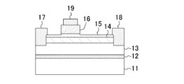
図1は本発明の第1の実施形態に係る窒化物半導体装置(JFET)の断面構成を示している。図1に示すように、第1の実施形態に係る窒化物半導体装置は、主面の面方位が(0001)面であるサファイアからなる基板11と、該基板11の主面上に形成された厚さが100nmの窒化アルミニウム(AlN)からなるバッファ層12と、該バッファ層12の上に設けられた厚さが2μmのアンドープの窒化ガリウム(GaN)からなるチャネル層13と、該チャネル層13の上に形成された厚さが25nmのアンドープの窒化アルミニウムガリウム(AlGaN)からなるバリア層14と、該バリア層14の上に形成された第1のp型層としての厚さが15nmのp型AlGaN層15と、該p型AlGaN層15上のゲート形成領域であり、第2のp型層としての厚さが100nmのp型GaN層16とを有している。ここで、アンドープとは、導電型を決定する不純物が意図的に導入されていないことを意味する。
FIG. 1 shows a cross-sectional configuration of a nitride semiconductor device (JFET) according to a first embodiment of the present invention. As shown in FIG. 1, the nitride semiconductor device according to the first embodiment is formed on a
p型AlGaN層15は、濃度が1×1019cm−3程度のマグネシウム(Mg)がドーピングされ、キャリア濃度は1×1018cm−3程度である。p型GaN層16は大部分がp型AlGaN層15と同程度のキャリア濃度を有し、その上面から厚さが約10nmの領域にはMgが1×1020cm−3程度の濃度にドーピングされている。
The p-
バリア層14とp型AlGaN層15とは、例えばAl0.15Ga0.85Nにより構成されている。
The
p型AlGaN層15及びバリア層14におけるp型GaN層16の両側方にはチャネル層13の上部を掘り込んだ開口部が設けられ、該開口部にはバリア層14とチャネル層13とのヘテロ界面に対して横方向から接触するように、Ti層とAl層とからなるソース電極17及びドレイン電極18が設けられている。このように、p型AlGaN層15、バリア層14及びチャネル層13の上部を掘り込み、バリア層14とチャネル層13とのヘテロ界面の近傍に形成される2次元電子ガス(2DEG)層と直接に接触するようにソース電極17及びドレイン電極18を形成することにより、該ソース電極17及びドレイン電極18をp型AlGaN層15の上に直接に形成した場合よりも大幅に接触抵抗を低減することができる。その上、p型AlGaN層15及びバリア層14の膜厚に依存せずに接触抵抗が小さいオーミック接合を得ることができる。
On both sides of the p-
p型AlGaN層15の上に選択的に形成されたp型GaN層16の上には、該p型GaN層16とオーミック接合するパラジウム(Pd)からなるゲート電極19が形成されている。ここで、p型GaN層16及びゲート電極19は、ソース電極17とドレイン電極18との中間位置からソース電極17側に偏った位置に設けられている。これは、ゲート電極19とドレイン電極18との間隔をゲート電極19とソース電極17との間隔よりも大きくすることによって、高いドレイン電圧が印加されたときに生じる電界を緩和して、トランジスタの破壊耐圧を向上するためである。
On the p-
図2は図1に示す窒化物半導体装置に対して、ゲート電極19とドレイン電極18とに同一周期のパルス電圧を印加した際のドレイン電流Idとドレイン電圧Vdsとの関係を表わしている。ここで、ゲート電極19及びドレイン電極18に印加されるパルス電圧のパルス幅は0.5μsとし、パルス間隔は1msとしている。
FIG. 2 shows the relationship between the drain current Id and the drain voltage Vds when a pulse voltage having the same period is applied to the
図2において、プロットAはパルス電圧を印加する前のバイアス条件として、ゲート電圧及びドレイン電圧が共に0Vの場合であり、プロットBはゲート電圧が0Vで且つドレイン電圧が60Vの場合を表わしている。図2のプロットBに示すように、ゲート電圧Vgsが1Vから5Vのいずれであっても、また、ドレイン電圧Vdsが10Vから60Vのいずれであっても、高いドレイン電圧が印加されないプロットAの場合の特性とほぼ一致していることから、オン抵抗も変わらず、従って電流コラプスが抑制されていることが分かる。 In FIG. 2, plot A shows a case where the gate voltage and the drain voltage are both 0 V as a bias condition before applying the pulse voltage, and plot B shows a case where the gate voltage is 0 V and the drain voltage is 60 V. . As shown in plot B of FIG. 2, in the case of plot A in which a high drain voltage is not applied regardless of whether the gate voltage Vgs is 1 V to 5 V or the drain voltage Vds is 10 V to 60 V. Since the on-resistance does not change, the current collapse is suppressed.
以下に、第1の実施形態に係る窒化物半導体装置が電流コラプスを抑制できる理由を説明する。 The reason why the nitride semiconductor device according to the first embodiment can suppress current collapse will be described below.
従来例に係る窒化物半導体装置においては、バリア層104におけるゲート電極108の側方部分に表面準位が形成され、この形成された表面準位にトラップされる電子によって生じる空乏層がチャネル(2DEG)に影響を及ぼすが、第1の実施形態に係る窒化物半導体装置においては、p型AlGaN層15におけるゲート電極19の側方部分に形成される表面準位がチャネルに与える影響が小さいためであると考えられる。
In the nitride semiconductor device according to the conventional example, a surface level is formed in a side portion of the
すなわち、従来例に係るトランジスタは、図12のプロットBに示したように、パルスが印加される直前の高いドレイン電圧が印加されている場合には、バリア層104におけるゲート電極108の側方部分に形成される表面準位にトラップされた電子によって空乏層がチャネルにまで広がっている。これにより、パルスの印加直後にゲート電極108の下側に位置するチャネルがオン状態となっても、表面準位にトラップされた電子の放出時間が遅いため、ゲートドレイン間に位置するチャネルがオン状態とはならない。その結果、高いドレイン電圧を印加せず電子トラップによる空乏層が広がってはいないプロットAに示す場合と比較してドレイン電流が減少してしまう。
That is, in the transistor according to the conventional example, as shown in plot B of FIG. 12, when a high drain voltage just before the pulse is applied is applied, the side portion of the
これに対し、本実施形態に係る窒化物半導体装置は、バリア層14の上にp型AlGaN層15を設けたことにより、パルスが印加される直前の高いドレイン電圧が印加されている場合に、p型AlGaN層15の表面準位にトラップされた電子よって生じる空乏層はチャネルにまでは到達しない。このため、チャネルにおけるゲート電極19の側方部分は常にオン状態となっている。これにより、パルスが印加された直後にゲート電極19の直下に位置するチャネルがオン状態となると、ソースドレイン間に位置するチャネルが全開状態となるため、高いドレイン電圧を印加していない場合、すなわち電子のトラップによる空乏層が広がっていない場合と比較しても同等のドレイン電流を得ることができる。
On the other hand, in the nitride semiconductor device according to the present embodiment, when the p-
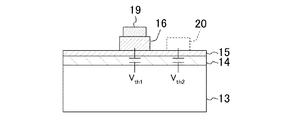
本実施形態に係る窒化物半導体装置において電流コラプスが抑制されるメカニズムを図3に基づいてより詳細に説明する。図3は図1に示す窒化物半導体装置の要部であって、ゲート電極19によるトランジスタの第1の閾値電圧Vth1と、ゲート電極19の側方に形成される仮想ゲート電極20による仮想トランジスタの第2の閾値電圧Vth2との模式的な断面構成を示している。
The mechanism by which current collapse is suppressed in the nitride semiconductor device according to the present embodiment will be described in more detail with reference to FIG. FIG. 3 shows the main part of the nitride semiconductor device shown in FIG. 1, in which the first threshold voltage V th1 of the transistor formed by the
前述したように、JFET構造は、チャネルにおけるゲート電極19の直下の領域の2次元電子ガス濃度を、その領域以外の2次元電子ガス濃度よりも選択的に小さくすることができる。このため、ゲート電極19の直下に位置するチャネルがオン状態となる第1の閾値電圧Vth1は、ゲート電極19の側方領域において表面空乏層を介して仮想的に形成される仮想トランジスタの第2の閾値電圧Vth2よりも大きくなる。このとき、仮想ゲート電極20は、p型AlGaN層15とはエネルギー障壁が0.7eV程度のショットキ接合を形成していると仮定する。第1の閾値電圧Vth1はアンドープのAlGaNからなるバリア層14における膜厚及びAlの組成比を調整することによって、負から正の値に制御することが可能である。
As described above, the JFET structure can selectively reduce the two-dimensional electron gas concentration in the region immediately below the
ゲート電極19に電圧を印加していないときには、仮想ゲート電極20の直下に位置するバリア層14とチャネル層13とのヘテロ界面には2次元電子ガスが生じているため、第2の閾値電圧Vth2は負の値となる。この第2の閾値電圧Vth2が負側にシフトする程、チャネル内の2次元電子ガスを空乏化するには、仮想ゲート電極20が接触しているp型AlGaN層15の表面に、より大きい負電荷が必要であることを意味している。
When no voltage is applied to the
このように、第1の実施形態に係る窒化物半導体装置のゲートドレイン間において、p型AlGaN層15をバリア層14の上に設けたことより、該p型AlGaN層15に形成される表面準位にトラップされる電子によって、チャネルがオフ状態となりにくいことを表わしている。
As described above, the p-
図4は第1の実施形態に係る窒化物半導体装置において、p型AlGaN層15及びバリア層14の膜厚を変化させた場合における第1の閾値電圧Vth1と第2の閾値電圧Vth2の差ΔVth(=Vth1−Vth2)とパルス電圧印加時のドレイン電流比との関係を示している。ここで、ドレイン電流比とは、パルス電圧印加時のドレイン電圧が10Vで且つゲート電圧が5Vの場合のドレイン電流において、パルス電圧を印加する直前のドレイン電圧が0Vの場合に対する60Vの場合の比を表わしている。従って、ドレイン電流比の値が1に近い程、電流コラプスが抑制されていることを示す。
FIG. 4 shows the first threshold voltage V th1 and the second threshold voltage V th2 when the thicknesses of the p-
図4に示すように、閾値電圧の差ΔVthとドレイン電流比の値との間には明確な相関関係があり、閾値電圧の差ΔVthが大きい程、電流コラプスが抑制される。特に、閾値電圧の差ΔVthが2.5V以上であれば、ドレイン電流比はほぼ1となり、完全に電流コラプスが抑制できることが分かる。 As shown in FIG. 4, there is a clear correlation between the threshold voltage difference ΔV th and the drain current ratio value, and the larger the threshold voltage difference ΔV th is, the more current collapse is suppressed. In particular, when the threshold voltage difference ΔV th is 2.5 V or more, the drain current ratio is almost 1, which indicates that current collapse can be completely suppressed.
ところで、閾値電圧の差ΔVthを大きくするには、p型AlGaN層15の厚膜化が有効である。
By the way, to increase the threshold voltage difference ΔV th , it is effective to increase the thickness of the p-
図5は第1の実施形態に係る窒化物半導体半導体装置におけるp型AlGaN層15の膜厚と閾値電圧の差ΔVthとの関係を示している。p型AlGaN層15の膜厚を大きくすると、第1の閾値電圧Vth1をほとんど変化させることなく、第2の閾値電圧Vth2を負側にシフトすることができる。このため、閾値電圧の差ΔVthを大きくすることが可能となるので、オン抵抗が増大せず、すなわち電流コラプスを抑制することができる。
FIG. 5 shows the relationship between the film thickness of the p-
アンドープAlGaNからなるバリア層14の膜厚を大きくする、又はAlの組成比を大きくすると、第2の閾値電圧Vth2を負側にシフトさせることができるが、これと同時に第1の閾値電圧Vth1も負側にシフトしてしまうため、閾値電圧の差ΔVthを大きくすることが不可能であり、さらにはノーマリオフ状態を維持することすら困難となる。
When the thickness of the
そこで、第1の実施形態においては、バリア層14の上に、より詳細にはバリア層14の上におけるゲート電極19の両側方の領域に、p型AlGaN層15を設けることによって、ノーマリオフ状態を維持できると同時に閾値電圧の差ΔVthを大きくすることができ、電流コラプスを抑制することができる。特に、図4及び図5から、閾値電圧の差ΔVthを2.5V以上とし、電流コラプスを完全に抑制するためには、p型AlGaN層15の膜厚を15nm以上とすることが有効であることが分かる。但し、p型AlGaN層15を厚くし過ぎると、該p型AlGaN層15を介してゲートドレイン間又はゲートソース間にリーク電流が流れてしまうため、p型AlGaN層15の膜厚は30nm程度以下であることが望ましい。
Therefore, in the first embodiment, by providing the p-
以下、前記のように構成された窒化物半導体装置の製造方法について図面を参照しながら説明する。 Hereinafter, a method for manufacturing the nitride semiconductor device configured as described above will be described with reference to the drawings.
図6(a)〜図6(e)は本実施形態に係る窒化物半導体装置の製造方法の工程順の断面構成を示している。 FIG. 6A to FIG. 6E show cross-sectional structures in the order of steps in the method for manufacturing a nitride semiconductor device according to this embodiment.
まず、図6(a)に示すように、例えば有機金属気相成長(MOCVD:Metal Organic Chemical Vapor Deposition)法により、主面の面方位が(0001)面であるサファイアからなる基板11の主面上に、厚さが100nmのAlNからなるバッファ層12、厚さが2μmのアンドープのGaNからなるチャネル層13、厚さが25nmのアンドープのAlGaNからなるバリア層14、厚さが15nmのp型AlGaN層15及び厚さが100nmのp型GaN層16をエピタキシャル成長により順次形成して、エピタキシャル成長層を形成する。
First, as shown in FIG. 6A, the main surface of the
次に、図6(b)に示すように、例えば、リソグラフィ法並びに塩素(Cl2)ガス及び六フッ化硫黄(SF6)ガスをエッチングガスとする誘導結合プラズマ(ICP:Inductive−Coupled Plasma)等を用いたドライエッチング法により、エピタキシャル成長層のp型GaN層16におけるゲート形成領域を除く部分に対して選択的にエッチングを行なう。このとき、GaN層とAlGaN層とのエッチングレートがほぼ同一である等速エッチングを用いてp型AlGaN層15を露出させることは可能ではあるが、より再現性を高めるには、GaN層のエッチングレートがAlGaN層よりも速くなる選択エッチングを用いることが有効である。
Next, as shown in FIG. 6B, for example, lithography and inductively coupled plasma (ICP) using an etching gas of chlorine (Cl 2 ) gas and sulfur hexafluoride (SF 6 ) gas are used. Etching is selectively performed on the portion of the p-
次に、図6(c)に示すように、例えば、リソグラフィ法及び塩素ガスを用いたICPエッチング等のドライエッチング法により、エピタキシャル層におけるソース電極及びドレイン電極の各形成領域となる凹部13aを、p型AlGaN層15、バリア層14及びチャネル層13の上部を選択的に除去することにより形成する。
Next, as shown in FIG. 6C, the
次に、図6(d)に示すように、例えばリフトオフ法により、形成した凹部13aに、それぞれTi層及びAl層からなる積層構造を有するソース電極17及びドレイン電極18を形成する。その後、温度が650℃の窒素(N2)雰囲気で熱処理(アニール)を行なう。
Next, as shown in FIG. 6D, a
次に、図6(e)に示すように、例えばリフトオフ法により、p型GaN層16の上にPdからなるゲート電極19を選択的に形成する。以上のようにして、第1の実施形態に係る窒化物半導体装置を得ることができる。
Next, as shown in FIG. 6E, a
(第1の実施形態の第1変形例)
第1の実施形態においては、図1に示すように、バリア層14の上に設けたp型AlGaN層15は、ゲート電極19の下側部分の厚さとその側方部分との厚さを実質的に同一としている。
(First modification of the first embodiment)
In the first embodiment, as shown in FIG. 1, the p-
しかしながら、図7に示す第1変形例のように、p型AlGaN層15におけるゲート電極19の下側部分の厚さを20nm程度とし、p型AlGaN層15におけるゲート電極19の側方部分の厚さを15nm程度として、ゲート電極19の側方部分の厚さをゲート電極19の下側部分の厚さよりも小さくしてもよい。
However, as in the first modification shown in FIG. 7, the thickness of the lower portion of the
これにより、第1変形例に係る窒化物半導体装置は、第1の実施形態と同様に電流コラプスを抑制できると共に、さらには、高いドレイン電圧が印加された場合に、電界強度が最大となるゲート電極19の側方に形成される段差部がバンドギャップエネルギーが大きいp型AlGaN層15のみで形成されるため、トランジスタの破壊耐圧を向上することができる。
Thereby, the nitride semiconductor device according to the first modification can suppress the current collapse as in the first embodiment, and further, the gate having the maximum electric field strength when a high drain voltage is applied. Since the step portion formed on the side of the
(第1の実施形態の第2変形例)
図8に示す第2変形例に係る窒化物半導体装置のように、p型GaN層16がゲート電極19の下側にのみ形成される構成ではなく、該p型GaN層16の一部がゲート電極19の側方にも形成される構成であってもよい。このとき、p型GaN層16におけるゲート電極19の側方の領域に形成された露出部分が厚いと、ゲートドレイン間又はゲートソース間に生じるリーク電流が増大する原因となるため、露出部分の厚さは20nm程度以下とすることが望ましい。これにより、前述した閾値電圧の差ΔVthを大きくすることができるため、電流コラプスを抑制することができる。
(Second modification of the first embodiment)
Unlike the nitride semiconductor device according to the second modification shown in FIG. 8, the p-
(第2の実施形態)
以下、本発明の第2の実施形態について図面を参照しながら説明する。
(Second Embodiment)
Hereinafter, a second embodiment of the present invention will be described with reference to the drawings.
図9は本発明の第2の実施形態に係る窒化物半導体装置の断面構成を示している。図9に示すように、導電性を有する基板の一例として、主面の面方位が(111)面であるn型シリコン(Si)からなる基板21の主面上に、第1の実施形態と同等のエピタキシャル層が形成されている。すなわち、基板21の上には、MOCVD法等により、AlNからなるバッファ層22、GaNからなるチャネル層23、アンドープのAlGaNからなるバリア層24、p型AlGaN層25及びp型GaN層26が順次形成されている。
FIG. 9 shows a cross-sectional configuration of a nitride semiconductor device according to the second embodiment of the present invention. As shown in FIG. 9, as an example of a conductive substrate, the main surface of a
p型GaN層26は、Pdからなるゲート電極29のほぼ下側部分にのみ選択的に形成されている。
The p-
TiとAlとからなるソース電極27及びドレイン電極28は、それぞれチャネル層23の上部に達する凹部に形成されている。
The
また、p型AlGaN層25の上には、窒化シリコン(SiN)からなるパッシベーション膜30がゲート電極29及びp型GaN層26を覆うように全面的に形成されている。
A
第2の実施形態の特徴として、ソース電極27のゲート電極29と反対側の領域(外側領域)には、パッシベーション膜30、p型AlGaN層25、バリア層24、チャネル層23及びバッファ層22を貫通するようにバイアホール21aが形成されている。ソース電極27は、該ソース電極27とバリアホール21aとに跨って形成されたアルミニウム(Al)からなるメタル配線31により基板21と電気的に接続されている。
As a feature of the second embodiment, a
基板21のバッファ層22と反対側の面(裏面)上にはAuGeSb合金からなる裏面電極32が形成されている。
A
パッシベーション膜30の上には、メタル配線31を含む全面にわたって、膜厚が約5μmで且つ比誘電率が3程度のポリイミド樹脂からなる層間膜33が形成されている。
On the
層間膜33にはドレイン電極28を露出するコンタクトホールが形成され、形成されたコンタクトホールを埋めることにより、一端がドレイン電極28と接触すると共に他端が層間膜33上をソース電極27の上方にまで延びる、Alからなる上部ドレイン電極34が形成されている。
A contact hole exposing the
このような構成により、ソース電圧は基板21の裏面に形成された裏面電極32を通して印加でき、一方、ドレイン電圧はゲート電極29の上方に形成された上部ドレイン電極34を通して印加することができるため、電極パッドをトランジスタ素子の活性領域の外側に形成する必要がなくなるので、チップサイズを縮小することができる。
With this configuration, the source voltage can be applied through the
また、ソース電極27は裏面電極32と接続され、ドレイン電極28は上部ドレイン電極34と接続されるため、新たなソース用及びドレイン用の電極用配線を設ける必要がなくなる。その結果、各電極用配線による配線抵抗が低減できるため、実装後のトランジスタのオン抵抗を低減することができる。
Further, since the
また、層間膜33には、比誘電率が低いポリイミド樹脂を用いているため、上部ドレイン電極34による寄生容量を低減することができるので、トランジスタのスイッチング速度をも向上することができる。なお、層間膜33の比誘電率は4以下であれば、寄生容量の低減に有効である。
Further, since the polyimide film having a low relative dielectric constant is used for the
なお、導電性を有する基板21はシリコン(Si)に限られず、炭化シリコン(SiC)を用いることができる。
Note that the
(第3の実施形態)
以下、本発明の第3の実施形態について図面を参照しながら説明する。
(Third embodiment)
Hereinafter, a third embodiment of the present invention will be described with reference to the drawings.
図10は本発明の第3の実施形態に係る窒化物半導体装置の断面構成を示している。図10に示すように、第3の実施形態に係る窒化物半導体装置は、主面の面方位が(0001)面であるサファイアからなる基板41と、該基板41の主面上に形成された厚さが100nmのAlNからなるバッファ層42と、該バッファ層42の上に設けられた厚さが2μmのアンドープのGaNからなるチャネル層43と、該チャネル層43の上に形成された厚さが25nmのアンドープのAlGaNからなるバリア層44と、該バリア層44の上に形成され、Pdからなるゲート電極48の下側部分の厚さが100nmで且つゲート電極48の側方部分の厚さが約15nmのp型GaN層45とを有している。
FIG. 10 shows a cross-sectional configuration of a nitride semiconductor device according to the third embodiment of the present invention. As shown in FIG. 10, the nitride semiconductor device according to the third embodiment is formed on a
p型GaN層45は、濃度が1×1019cm−3程度のMgがドーピングされ、キャリア濃度は1×1018cm−3程度であり、ゲート電極48の下側部分はその上面から厚さが約10nmの領域にはMgが1×1020cm−3程度の濃度にドーピングされている。
The p-
バリア層44は、例えばAl0.15Ga0.85Nにより構成されている。
The
p型GaN層45及びバリア層44におけるゲート電極48の両側方にはチャネル層43の上部を掘り込んだ開口部が設けられ、該開口部にはバリア層44とチャネル層43とのヘテロ界面に対して横方向から接触するように、Ti層とAl層とからなるソース電極46及びドレイン電極47が設けられている。
On both sides of the
また、ゲート電極48は、ソース電極46側に偏った位置に設けられている。
The
このように、第3の実施形態に係る窒化物半導体装置は、アンドープのAlGaNからなるバリア層44の上に、ゲート電極48の下側部分の厚さが100nmで且つゲート電極48の側方部分の厚さが15nm程度のp型GaN層45を設けている。
As described above, in the nitride semiconductor device according to the third embodiment, the thickness of the lower part of the
このように、第3の実施形態に係るp型GaN層45は、ゲート電極48の下側部分と側方部分との厚さを変えてはいるものの、一体に形成されている。このようにしても、前述した、本トランジスタ素子と仮想トランジスタ素子との閾値電圧の差ΔVthを大きくすることができるため、電流コラプスを抑制することができる。
As described above, the p-
ところで、AlGaN層はGaN層とは格子定数が異なるため、AlGaN層の膜厚が大きくなると結晶成長が困難となるが、第3の実施形態に係る窒化物半導体装置は、第1及び第2の実施形態のように、アンドープのAlGaNからなるバリア層とp型GaN層との間にp型AlGaN層を設けないため、結晶成長が容易である。 By the way, since the AlGaN layer has a lattice constant different from that of the GaN layer, the crystal growth becomes difficult when the thickness of the AlGaN layer is increased. However, the nitride semiconductor device according to the third embodiment has the first and second structures. Since the p-type AlGaN layer is not provided between the barrier layer made of undoped AlGaN and the p-type GaN layer as in the embodiment, crystal growth is easy.
なお、p型GaN層45におけるゲート電極48の側方部分の膜厚が大きくなるとゲートドレイン間又はゲートソース間のリーク電流が増大する原因となるため、p型GaN層45におけるゲート電極48の側方部分の膜厚は20nm程度以下とすることが望ましい。
Note that if the thickness of the side portion of the
なお、第3の実施形態に係る半導体装置の製造方法は、MOCVD法等により、基板41の上にバリア層42からp型GaN層45までを順次エピタキシャル成長した後、p型GaN層におけるゲート電極形成領域の側方部分に対してのみ選択的にドライエッチングを行なえばよい。
Note that in the method of manufacturing the semiconductor device according to the third embodiment, after sequentially growing the
本発明に係る窒化物半導体装置及びその製造方法は、オン抵抗が小さく且つ電流コラプスが抑制されたノーマリオフ型の窒化物半導体装置を実現することができ、電源回路等に用いられるパワートランジスタとして有用である。 INDUSTRIAL APPLICABILITY The nitride semiconductor device and the manufacturing method thereof according to the present invention can realize a normally-off type nitride semiconductor device with low on-resistance and suppressed current collapse, and is useful as a power transistor used in a power supply circuit or the like. is there.
11 基板
12 バッファ層
13 チャネル層
13a 凹部
14 バリア層
15 p型AlGaN層(第1のp型層)
16 p型GaN層(第2のp型層)
17 ソース電極
18 ドレイン電極
19 ゲート電極
20 仮想ゲート電極
21 基板
21a バイアホール
22 バッファ層
33 チャネル層
24 バリア層
25 p型AlGaN層(第1のp型層)
26 p型GaN層(第2のp型層)
27 ソース電極
28 ドレイン電極
29 ゲート電極
30 パッシベーション膜
31 メタル配線
32 裏面電極
33 層間膜
34 上部ドレイン電極
41 基板
42 バッファ層
43 チャネル層
44 バリア層
45 p型GaN層
46 ソース電極
47 ドレイン電極
48 ゲート電極
11
16 p-type GaN layer (second p-type layer)
17
26 p-type GaN layer (second p-type layer)
27
Claims (17)
前記基板の上に形成された第1の窒化物半導体層と、
前記第1の窒化物半導体層の上に形成され、前記第1の窒化物半導体層よりもバンドギャップエネルギーが大きい第2の窒化物半導体層と、
前記第2の窒化物半導体層の上に形成され、p型の窒化物半導体よりなる第3の窒化物半導体層と、
前記第3の窒化物半導体層の上に形成されたゲート電極と、
前記ゲート電極の両側方にそれぞれ形成され、且つ前記第3の窒化物半導体層と接するソース電極及びドレイン電極とを備え、
前記第3の窒化物半導体層の前記ゲート電極の直下の部分の厚さは、前記ソース電極及び前記ドレイン電極と接する部分の厚さよりも大きいことを特徴とする窒化物半導体装置。 A substrate,
A first nitride semiconductor layer formed on the substrate;
A second nitride semiconductor layer formed on the first nitride semiconductor layer and having a band gap energy larger than that of the first nitride semiconductor layer;
A third nitride semiconductor layer formed on the second nitride semiconductor layer and made of a p-type nitride semiconductor;
A gate electrode formed on the third nitride semiconductor layer;
Wherein each is formed on both sides of the gate electrode, and source and drain electrodes and in contact with the third nitride semiconductor layer,
The nitride semiconductor device , wherein a thickness of a portion of the third nitride semiconductor layer immediately below the gate electrode is larger than a thickness of a portion in contact with the source electrode and the drain electrode .
前記第1のp型層は、前記ゲート電極の下側部分の厚さが、前記ソース電極と前記ゲート電極との間及び前記ドレイン電極と前記ゲート電極との間に位置する部分の厚さよりも大きいことを特徴とする請求項1に記載の窒化物半導体装置。 The third nitride semiconductor layer includes a first p-type layer and a second p-type layer sequentially formed from the substrate side,
In the first p-type layer, the thickness of the lower part of the gate electrode is larger than the thickness of the part located between the source electrode and the gate electrode and between the drain electrode and the gate electrode. The nitride semiconductor device according to claim 1, wherein the nitride semiconductor device is large.
前記第2のp型層は、前記ソース電極及び前記ドレイン電極と接触していることを特徴とする請求項1に記載の窒化物半導体装置。 The third nitride semiconductor layer includes a first p-type layer and a second p-type layer sequentially formed from the substrate side,
The nitride semiconductor device according to claim 1, wherein the second p-type layer is in contact with the source electrode and the drain electrode.
前記第2の窒化物半導体層は、AlxGa1−xN(0<x≦1)からなり、
前記第3の窒化物半導体層における前記第1のp型層は、AlyGa1−yN(0≦y≦1)からなり、
前記第3の窒化物半導体層における前記第2のp型層は、AlzGa1−zN(0≦z≦1,y≠z)からなることを特徴とする請求項2又は3に記載の窒化物半導体装置。 The first nitride semiconductor layer is made of GaN;
The second nitride semiconductor layer is made of Al x Ga 1-x N (0 <x ≦ 1),
The first p-type layer in the third nitride semiconductor layer is made of Al y Ga 1-y N (0 ≦ y ≦ 1),
The second p-type layer in the third nitride semiconductor layer is made of Al z Ga 1-z N (0 ≦ z ≦ 1, y ≠ z). Nitride semiconductor device.
前記絶縁膜の上に設けられ、前記ドレイン電極と電気的に接続された上部電極とをさらに備えていることを特徴とする請求項1〜12のいずれか1項に記載の窒化物半導体装置。 An insulating film formed on the gate electrode and having a relative dielectric constant of 4 or less;
Wherein provided on the insulating film, a nitride semiconductor device according to any one of claims 1 to 12, characterized by further comprising a said drain electrode and electrically connected to the upper electrode.
前記第4の窒化物半導体層におけるゲート電極形成領域を除く部分であって、前記第4の窒化物半導体層の上部又は前記第3の窒化物半導体層の上部を選択的に除去することにより、前記第4の窒化物半導体層から前記ゲート電極形成領域を形成する工程(b)と、
前記ゲート電極形成領域の両側方の領域で且つ前記ゲート電極形成領域から離れた領域であって、少なくとも前記第3の窒化物半導体層及び第2の窒化物半導体層並びに前記第1の窒化物半導体の上部を選択的に除去することにより、断面凹状のソースドレイン電極形成領域を形成する工程(c)と、
前記ソースドレイン形成領域に金属膜を形成することにより、前記第2の窒化物半導体層及び第1の窒化物半導体層の界面、並びに前記第3の窒化物半導体層の側部とそれぞれ接するソース電極及びドレイン電極を形成する工程(d)と、
前記ゲート電極形成領域の上にゲート電極を形成する工程(e)とを備えていることを特徴とする窒化物半導体装置の製造方法。 On the substrate, a first nitride semiconductor layer, a second nitride semiconductor layer having a band gap energy larger than that of the first nitride semiconductor, a p-type third nitride semiconductor layer, and a p-type first nitride semiconductor layer. Step (a) of sequentially forming the nitride semiconductor layers 4;
By selectively removing the upper portion of the fourth nitride semiconductor layer or the upper portion of the third nitride semiconductor layer, which is a portion excluding the gate electrode formation region in the fourth nitride semiconductor layer, Forming the gate electrode formation region from the fourth nitride semiconductor layer (b);
A region on both sides of the gate electrode formation region and a distance from the gate electrode formation region, at least the third nitride semiconductor layer, the second nitride semiconductor layer, and the first nitride semiconductor (C) forming a source / drain electrode formation region having a concave cross section by selectively removing the upper portion of
By forming a metal film in the source / drain formation region, the source electrode is in contact with the interface between the second nitride semiconductor layer and the first nitride semiconductor layer and the side portion of the third nitride semiconductor layer. And (d) forming a drain electrode;
And a step (e) of forming a gate electrode on the gate electrode formation region.
前記工程(c)において、前記第4の窒化物半導体層の残部における前記ソースドレイン電極形成領域をも選択的に除去することを特徴とする請求項14に記載の窒化物半導体装置の製造方法。 In the step (b), an upper portion of the fourth nitride semiconductor layer excluding the gate electrode formation region is selectively removed,
The method of manufacturing a nitride semiconductor device according to claim 14 , wherein in the step (c), the source / drain electrode formation region in the remaining portion of the fourth nitride semiconductor layer is also selectively removed.
前記第3の窒化物半導体層におけるゲート電極形成領域を除く部分であって、その上部を選択的に除去することにより、前記第3の窒化物半導体層から前記ゲート電極形成領域を形成する工程(b)と、
前記ゲート電極形成領域の両側方の領域で且つ前記ゲート電極形成領域から離れた領域であって、前記第3の窒化物半導体層の残部、前記第2の窒化物半導体層及び前記第1の窒化物半導体の上部を選択的に除去することにより、凹状のソースドレイン電極形成領域を形成する工程(c)と、
前記ソースドレイン形成領域に金属膜を形成することにより、前記第2の窒化物半導体層及び第1の窒化物半導体層の界面、並びに前記第3の窒化物半導体層の側部とそれぞれに接するソース電極及びドレイン電極を形成する工程(d)と、
前記ゲート電極形成領域の上にゲート電極を形成する工程(e)とを備えていることを特徴とする窒化物半導体装置の製造方法。 A step of sequentially forming a first nitride semiconductor layer, a second nitride semiconductor layer having a band gap energy larger than that of the first nitride semiconductor, and a p-type third nitride semiconductor layer on the substrate. (A) and
Forming the gate electrode formation region from the third nitride semiconductor layer by selectively removing the upper portion of the third nitride semiconductor layer excluding the gate electrode formation region ( b) and
A region on both sides of the gate electrode formation region and away from the gate electrode formation region, the remaining portion of the third nitride semiconductor layer, the second nitride semiconductor layer, and the first nitride A step (c) of forming a concave source / drain electrode formation region by selectively removing an upper portion of the physical semiconductor;
By forming a metal film in the source / drain formation region, the source is in contact with the interface between the second nitride semiconductor layer and the first nitride semiconductor layer and the side portion of the third nitride semiconductor layer. A step (d) of forming an electrode and a drain electrode;
And a step (e) of forming a gate electrode on the gate electrode formation region.
Priority Applications (3)
| Application Number | Priority Date | Filing Date | Title |
|---|---|---|---|
| JP2006267476A JP4755961B2 (en) | 2006-09-29 | 2006-09-29 | Nitride semiconductor device and manufacturing method thereof |
| US11/890,480 US7898002B2 (en) | 2006-09-29 | 2007-08-07 | Nitride semiconductor device and method for fabricating the same |
| US13/010,238 US8164115B2 (en) | 2006-09-29 | 2011-01-20 | Nitride semiconductor device |
Applications Claiming Priority (1)
| Application Number | Priority Date | Filing Date | Title |
|---|---|---|---|
| JP2006267476A JP4755961B2 (en) | 2006-09-29 | 2006-09-29 | Nitride semiconductor device and manufacturing method thereof |
Related Child Applications (2)
| Application Number | Title | Priority Date | Filing Date |
|---|---|---|---|
| JP2011020627A Division JP4815020B2 (en) | 2011-02-02 | 2011-02-02 | Nitride semiconductor device |
| JP2011095622A Division JP2011142358A (en) | 2011-04-22 | 2011-04-22 | Nitride semiconductor device |
Publications (3)
| Publication Number | Publication Date |
|---|---|
| JP2008091392A JP2008091392A (en) | 2008-04-17 |
| JP2008091392A5 JP2008091392A5 (en) | 2011-03-17 |
| JP4755961B2 true JP4755961B2 (en) | 2011-08-24 |
Family
ID=39260265
Family Applications (1)
| Application Number | Title | Priority Date | Filing Date |
|---|---|---|---|
| JP2006267476A Active JP4755961B2 (en) | 2006-09-29 | 2006-09-29 | Nitride semiconductor device and manufacturing method thereof |
Country Status (2)
| Country | Link |
|---|---|
| US (2) | US7898002B2 (en) |
| JP (1) | JP4755961B2 (en) |
Cited By (1)
| Publication number | Priority date | Publication date | Assignee | Title |
|---|---|---|---|---|
| US9269577B2 (en) | 2012-10-26 | 2016-02-23 | Furukawa Electric Co., Ltd. | Method for manufacturing nitride semiconductor device |
Families Citing this family (75)
| Publication number | Priority date | Publication date | Assignee | Title |
|---|---|---|---|---|
| JP4889203B2 (en) * | 2004-04-21 | 2012-03-07 | 新日本無線株式会社 | Nitride semiconductor device and manufacturing method thereof |
| JP4705412B2 (en) * | 2005-06-06 | 2011-06-22 | パナソニック株式会社 | Field effect transistor and manufacturing method thereof |
| JP4755961B2 (en) * | 2006-09-29 | 2011-08-24 | パナソニック株式会社 | Nitride semiconductor device and manufacturing method thereof |
| JP4712683B2 (en) * | 2006-12-21 | 2011-06-29 | パナソニック株式会社 | Transistor and manufacturing method thereof |
| JP5032965B2 (en) * | 2007-12-10 | 2012-09-26 | パナソニック株式会社 | Nitride semiconductor transistor and manufacturing method thereof |
| US8497527B2 (en) * | 2008-03-12 | 2013-07-30 | Sensor Electronic Technology, Inc. | Device having active region with lower electron concentration |
| JP2009289827A (en) * | 2008-05-27 | 2009-12-10 | Toyota Central R&D Labs Inc | Semiconductor device having heterojunction and manufacturing method thereof |
| JP5433175B2 (en) * | 2008-07-02 | 2014-03-05 | シャープ株式会社 | Semiconductor device |
| JP2010103236A (en) * | 2008-10-22 | 2010-05-06 | Panasonic Corp | Nitride semiconductor device |
| CN102388441B (en) * | 2009-04-08 | 2014-05-07 | 宜普电源转换公司 | Enhancement mode GaN HEMT device and method for fabricating the same |
| US8436398B2 (en) * | 2009-04-08 | 2013-05-07 | Efficient Power Conversion Corporation | Back diffusion suppression structures |
| US8823012B2 (en) | 2009-04-08 | 2014-09-02 | Efficient Power Conversion Corporation | Enhancement mode GaN HEMT device with gate spacer and method for fabricating the same |
| JP2012523699A (en) * | 2009-04-08 | 2012-10-04 | エフィシエント パワー コンヴァーション コーポレーション | Enhancement mode gallium nitride transistor with improved gate characteristics |
| JP5587564B2 (en) * | 2009-06-19 | 2014-09-10 | ルネサスエレクトロニクス株式会社 | Field effect transistor and method of manufacturing field effect transistor |
| JP5595685B2 (en) * | 2009-07-28 | 2014-09-24 | パナソニック株式会社 | Semiconductor device |
| DE102009028918B4 (en) * | 2009-08-26 | 2014-11-06 | Fraunhofer-Gesellschaft zur Förderung der angewandten Forschung e.V. | Semiconductor device, method for determining the structure of a transistor and base station for a mobile radio network |
| JP5530682B2 (en) * | 2009-09-03 | 2014-06-25 | パナソニック株式会社 | Nitride semiconductor device |
| TW201112440A (en) * | 2009-09-29 | 2011-04-01 | Ubilux Optoelectronics Corp | Manufacturing method of vertical light emitting diode |
| JP5899519B2 (en) * | 2009-11-05 | 2016-04-06 | パナソニックIpマネジメント株式会社 | Solid-state imaging device |
| US20110147796A1 (en) | 2009-12-17 | 2011-06-23 | Infineon Technologies Austria Ag | Semiconductor device with metal carrier and manufacturing method |
| JP5655333B2 (en) * | 2010-03-19 | 2015-01-21 | 日本電気株式会社 | Semiconductor structure and manufacturing method thereof |
| JP5725749B2 (en) * | 2010-07-28 | 2015-05-27 | 住友電工デバイス・イノベーション株式会社 | Manufacturing method of semiconductor device |
| JP2012033689A (en) * | 2010-07-30 | 2012-02-16 | Sumitomo Electric Device Innovations Inc | Manufacturing method of semiconductor device |
| JP5605134B2 (en) * | 2010-09-30 | 2014-10-15 | 富士通セミコンダクター株式会社 | Semiconductor device and manufacturing method thereof |
| CN103493205A (en) * | 2011-05-20 | 2014-01-01 | 松下电器产业株式会社 | Schottky diode |
| US8604486B2 (en) * | 2011-06-10 | 2013-12-10 | International Rectifier Corporation | Enhancement mode group III-V high electron mobility transistor (HEMT) and method for fabrication |
| WO2013011617A1 (en) * | 2011-07-15 | 2013-01-24 | パナソニック株式会社 | Semiconductor device and method for manufacturing same |
| JP2013062494A (en) * | 2011-08-24 | 2013-04-04 | Sanken Electric Co Ltd | Nitride semiconductor device |
| JP2013074179A (en) * | 2011-09-28 | 2013-04-22 | Fujitsu Ltd | Compound semiconductor device and manufacturing method of the same |
| US9018677B2 (en) * | 2011-10-11 | 2015-04-28 | Taiwan Semiconductor Manufacturing Company, Ltd. | Semiconductor structure and method of forming the same |
| JP5680223B2 (en) * | 2011-12-27 | 2015-03-04 | シャープ株式会社 | Normally-off heterojunction field effect transistor |
| US8963162B2 (en) * | 2011-12-28 | 2015-02-24 | Taiwan Semiconductor Manufacturing Company, Ltd. | High electron mobility transistor |
| DE102013202972B4 (en) * | 2012-02-23 | 2020-07-30 | Efficient Power Conversion Corporation | Enrichment operation of a GaN-HEMT device with a GATE spacer and method for its production |
| US10269658B2 (en) | 2012-06-29 | 2019-04-23 | Taiwan Semiconductor Manufacturing Company, Ltd. | Integrated circuit devices with well regions and methods for forming the same |
| TWI481026B (en) * | 2012-08-07 | 2015-04-11 | Richtek Technology Corp | High electron mobility transistor and manufacturing method thereof |
| CN103579299B (en) * | 2012-08-09 | 2016-04-13 | 立锜科技股份有限公司 | High Electron Mobility Transistor and manufacture method thereof |
| US9917080B2 (en) * | 2012-08-24 | 2018-03-13 | Qorvo US. Inc. | Semiconductor device with electrical overstress (EOS) protection |
| JP2014060358A (en) * | 2012-09-19 | 2014-04-03 | Toshiba Corp | Semiconductor device |
| US9064709B2 (en) * | 2012-09-28 | 2015-06-23 | Intel Corporation | High breakdown voltage III-N depletion mode MOS capacitors |
| JP2014072377A (en) | 2012-09-28 | 2014-04-21 | Fujitsu Ltd | Compound semiconductor device and manufacturing method of the same |
| KR101922122B1 (en) * | 2012-09-28 | 2018-11-26 | 삼성전자주식회사 | Normally off high electron mobility transistor |
| US10134727B2 (en) | 2012-09-28 | 2018-11-20 | Intel Corporation | High breakdown voltage III-N depletion mode MOS capacitors |
| KR101922121B1 (en) | 2012-10-09 | 2018-11-26 | 삼성전자주식회사 | High electron mobility transistor and method of manufacturing the same |
| KR102055839B1 (en) | 2013-03-08 | 2019-12-13 | 삼성전자주식회사 | Nitride based semiconductor device |
| KR102036349B1 (en) | 2013-03-08 | 2019-10-24 | 삼성전자 주식회사 | High electron mobility transistors |
| US9443737B2 (en) * | 2013-04-03 | 2016-09-13 | Texas Instruments Incorporated | Method of forming metal contacts in the barrier layer of a group III-N HEMT |
| JPWO2015008430A1 (en) * | 2013-07-16 | 2017-03-02 | パナソニックIpマネジメント株式会社 | Semiconductor device |
| US9978844B2 (en) | 2013-08-01 | 2018-05-22 | Taiwan Semiconductor Manufacturing Co., Ltd. | HEMT-compatible lateral rectifier structure |
| KR101729653B1 (en) * | 2013-12-30 | 2017-04-25 | 한국전자통신연구원 | Nitride semiconductor device |
| JP2015173151A (en) * | 2014-03-11 | 2015-10-01 | 株式会社東芝 | semiconductor device |
| WO2015163916A1 (en) * | 2014-04-25 | 2015-10-29 | Hrl Laboratories, Llc | Fet transistor on a iii-v material structure with substrate transfer |
| JP2016063167A (en) * | 2014-09-19 | 2016-04-25 | 株式会社東芝 | Semiconductor device |
| US10396081B2 (en) * | 2014-11-04 | 2019-08-27 | Sony Corporation | Semiconductor device, antenna switch circuit, and wireless communication apparatus |
| US10062684B2 (en) | 2015-02-04 | 2018-08-28 | Qorvo Us, Inc. | Transition frequency multiplier semiconductor device |
| US10615158B2 (en) | 2015-02-04 | 2020-04-07 | Qorvo Us, Inc. | Transition frequency multiplier semiconductor device |
| US9871067B2 (en) * | 2015-11-17 | 2018-01-16 | Taiwan Semiconductor Manufacturing Co., Ltd. | Infrared image sensor component |
| US9837523B2 (en) * | 2015-12-23 | 2017-12-05 | Synopsys, Inc. | Tined gate to control threshold voltage in a device formed of materials having piezoelectric properties |
| JP6584987B2 (en) * | 2016-03-23 | 2019-10-02 | 株式会社東芝 | Semiconductor device |
| US9673311B1 (en) * | 2016-06-14 | 2017-06-06 | Semiconductor Components Industries, Llc | Electronic device including a multiple channel HEMT |
| US10395965B2 (en) * | 2016-08-23 | 2019-08-27 | QROMIS, Inc. | Electronic power devices integrated with an engineered substrate |
| TWI612662B (en) * | 2017-01-09 | 2018-01-21 | 國立臺灣師範大學 | Semiconductor device and method of manufacturing the same |
| EP3442026B1 (en) * | 2017-08-11 | 2023-03-08 | IMEC vzw | Gate for an enhancement-mode transistor |
| GB2565805B (en) | 2017-08-23 | 2020-05-13 | X Fab Semiconductor Foundries Gmbh | Noff III-nitride high electron mobility transistor |
| KR102064752B1 (en) * | 2018-08-22 | 2020-01-10 | 주식회사 시지트로닉스 | Structure and fabrication method of SAG-GaN Power FET using side wall structure |
| CN110071173B (en) * | 2019-04-30 | 2023-04-18 | 英诺赛科(珠海)科技有限公司 | Semiconductor device and method for manufacturing the same |
| US11784232B2 (en) * | 2019-06-04 | 2023-10-10 | Nippon Telegraph And Telephone Corporation | Field effect transistor and method for manufacturing the same |
| CN110600548A (en) * | 2019-09-20 | 2019-12-20 | 中国电子科技集团公司第十三研究所 | Enhancement mode heterojunction field effect transistor |
| CN113224154B (en) * | 2020-02-06 | 2023-08-08 | 联华电子股份有限公司 | High electron mobility transistor and manufacturing method thereof |
| US20220109056A1 (en) * | 2020-04-16 | 2022-04-07 | Innoscience (Zhuhai) Technology Co., Ltd. | Semiconductor device and fabrication method thereof |
| US11522077B2 (en) * | 2020-05-27 | 2022-12-06 | Taiwan Semiconductor Manufacturing Company, Ltd. | Integration of p-channel and n-channel E-FET III-V devices with optimization of device performance |
| US11677002B2 (en) * | 2020-09-16 | 2023-06-13 | Vanguard International Semiconductor Corporation | Semiconductor structure |
| US20220130988A1 (en) * | 2020-10-27 | 2022-04-28 | Texas Instruments Incorporated | Electronic device with enhancement mode gallium nitride transistor, and method of making same |
| TWI780513B (en) * | 2020-11-13 | 2022-10-11 | 國立中山大學 | P-GaN HIGH ELECTRON MOBILITY TRANSISTOR |
| US20220173234A1 (en) * | 2020-12-01 | 2022-06-02 | Texas Instruments Incorporated | Normally-on gallium nitride based transistor with p-type gate |
| WO2023189039A1 (en) * | 2022-03-30 | 2023-10-05 | ローム株式会社 | Nitride semiconductor device |
Citations (5)
| Publication number | Priority date | Publication date | Assignee | Title |
|---|---|---|---|---|
| US5866925A (en) * | 1997-01-09 | 1999-02-02 | Sandia Corporation | Gallium nitride junction field-effect transistor |
| JP2000349095A (en) * | 1999-06-04 | 2000-12-15 | Sony Corp | Semiconductor device and its manufacture, power amplifier, and wireless communication device |
| JP2005244072A (en) * | 2004-02-27 | 2005-09-08 | Toshiba Corp | Semiconductor device |
| JP2006032749A (en) * | 2004-07-20 | 2006-02-02 | Toyota Motor Corp | Semiconductor device and its manufacturing method |
| JP2007335508A (en) * | 2006-06-13 | 2007-12-27 | Nec Electronics Corp | Field effect transistor and its manufacturing method |
Family Cites Families (17)
| Publication number | Priority date | Publication date | Assignee | Title |
|---|---|---|---|---|
| JPH11261053A (en) | 1998-03-09 | 1999-09-24 | Furukawa Electric Co Ltd:The | High electron mobility transistor |
| US6593193B2 (en) * | 2001-02-27 | 2003-07-15 | Matsushita Electric Industrial Co., Ltd. | Semiconductor device and method for fabricating the same |
| JP2004273486A (en) | 2003-03-05 | 2004-09-30 | Mitsubishi Electric Corp | Semiconductor device and its manufacturing method |
| US7382001B2 (en) * | 2004-01-23 | 2008-06-03 | International Rectifier Corporation | Enhancement mode III-nitride FET |
| US7170111B2 (en) * | 2004-02-05 | 2007-01-30 | Cree, Inc. | Nitride heterojunction transistors having charge-transfer induced energy barriers and methods of fabricating the same |
| JP4489529B2 (en) * | 2004-07-28 | 2010-06-23 | 株式会社日立製作所 | Particle beam therapy system and control system for particle beam therapy system |
| US7476918B2 (en) * | 2004-11-22 | 2009-01-13 | Panasonic Corporation | Semiconductor integrated circuit device and vehicle-mounted radar system using the same |
| US7498617B2 (en) * | 2005-02-02 | 2009-03-03 | International Rectifier Corporation | III-nitride integrated schottky and power device |
| JP4705412B2 (en) * | 2005-06-06 | 2011-06-22 | パナソニック株式会社 | Field effect transistor and manufacturing method thereof |
| JP4712459B2 (en) * | 2005-07-08 | 2011-06-29 | パナソニック株式会社 | Transistor and method of operating the same |
| JP4705482B2 (en) * | 2006-01-27 | 2011-06-22 | パナソニック株式会社 | Transistor |
| JP2007220895A (en) * | 2006-02-16 | 2007-08-30 | Matsushita Electric Ind Co Ltd | Nitride semiconductor device and its manufacturing method |
| JP5147197B2 (en) * | 2006-06-06 | 2013-02-20 | パナソニック株式会社 | Transistor |
| US20080054300A1 (en) * | 2006-06-30 | 2008-03-06 | Philip Gene Nikkel | Body contact structure and method for the reduction of drain lag and gate lag in field effect transistors |
| JP4755961B2 (en) * | 2006-09-29 | 2011-08-24 | パナソニック株式会社 | Nitride semiconductor device and manufacturing method thereof |
| US7467918B2 (en) * | 2006-10-26 | 2008-12-23 | Deere & Company | Remote controlled latching system |
| JP5032965B2 (en) * | 2007-12-10 | 2012-09-26 | パナソニック株式会社 | Nitride semiconductor transistor and manufacturing method thereof |
-
2006
- 2006-09-29 JP JP2006267476A patent/JP4755961B2/en active Active
-
2007
- 2007-08-07 US US11/890,480 patent/US7898002B2/en active Active
-
2011
- 2011-01-20 US US13/010,238 patent/US8164115B2/en active Active
Patent Citations (5)
| Publication number | Priority date | Publication date | Assignee | Title |
|---|---|---|---|---|
| US5866925A (en) * | 1997-01-09 | 1999-02-02 | Sandia Corporation | Gallium nitride junction field-effect transistor |
| JP2000349095A (en) * | 1999-06-04 | 2000-12-15 | Sony Corp | Semiconductor device and its manufacture, power amplifier, and wireless communication device |
| JP2005244072A (en) * | 2004-02-27 | 2005-09-08 | Toshiba Corp | Semiconductor device |
| JP2006032749A (en) * | 2004-07-20 | 2006-02-02 | Toyota Motor Corp | Semiconductor device and its manufacturing method |
| JP2007335508A (en) * | 2006-06-13 | 2007-12-27 | Nec Electronics Corp | Field effect transistor and its manufacturing method |
Cited By (1)
| Publication number | Priority date | Publication date | Assignee | Title |
|---|---|---|---|---|
| US9269577B2 (en) | 2012-10-26 | 2016-02-23 | Furukawa Electric Co., Ltd. | Method for manufacturing nitride semiconductor device |
Also Published As
| Publication number | Publication date |
|---|---|
| US20080079023A1 (en) | 2008-04-03 |
| JP2008091392A (en) | 2008-04-17 |
| US20110114967A1 (en) | 2011-05-19 |
| US7898002B2 (en) | 2011-03-01 |
| US8164115B2 (en) | 2012-04-24 |
Similar Documents
| Publication | Publication Date | Title |
|---|---|---|
| JP4755961B2 (en) | Nitride semiconductor device and manufacturing method thereof | |
| JP4712459B2 (en) | Transistor and method of operating the same | |
| US8390029B2 (en) | Semiconductor device for reducing and/or preventing current collapse | |
| JP4705412B2 (en) | Field effect transistor and manufacturing method thereof | |
| JP5468768B2 (en) | Field effect transistor and manufacturing method thereof | |
| US8148752B2 (en) | Field effect transistor | |
| JP5487615B2 (en) | Field effect semiconductor device and manufacturing method thereof | |
| JP5147197B2 (en) | Transistor | |
| JP5032965B2 (en) | Nitride semiconductor transistor and manufacturing method thereof | |
| JP4940557B2 (en) | Field effect transistor and manufacturing method thereof | |
| JP5595685B2 (en) | Semiconductor device | |
| JP2007220895A (en) | Nitride semiconductor device and its manufacturing method | |
| JP2008098434A (en) | Nitride semiconductor transistor and its manufacturing method | |
| JP4815020B2 (en) | Nitride semiconductor device | |
| US9680001B2 (en) | Nitride semiconductor device | |
| US20150263155A1 (en) | Semiconductor device | |
| WO2013011617A1 (en) | Semiconductor device and method for manufacturing same | |
| JP2011142358A (en) | Nitride semiconductor device | |
| JP2011066464A (en) | Field effect transistor | |
| JP5721782B2 (en) | Semiconductor device | |
| JP2013239735A (en) | Field effect transistor | |
| JP2010245240A (en) | Heterojunction field-effect semiconductor device and method of manufacturing the same | |
| JP5898802B2 (en) | Field effect transistor | |
| JP2015056413A (en) | Nitride semiconductor device | |
| JP5739564B2 (en) | Field effect transistor |
Legal Events
| Date | Code | Title | Description |
|---|---|---|---|
| A521 | Written amendment |
Free format text: JAPANESE INTERMEDIATE CODE: A523 Effective date: 20090313 |
|
| A621 | Written request for application examination |
Free format text: JAPANESE INTERMEDIATE CODE: A621 Effective date: 20090313 |
|
| A521 | Written amendment |
Free format text: JAPANESE INTERMEDIATE CODE: A523 Effective date: 20110202 |
|
| A871 | Explanation of circumstances concerning accelerated examination |
Free format text: JAPANESE INTERMEDIATE CODE: A871 Effective date: 20110202 |
|
| A975 | Report on accelerated examination |
Free format text: JAPANESE INTERMEDIATE CODE: A971005 Effective date: 20110215 |
|
| A131 | Notification of reasons for refusal |
Free format text: JAPANESE INTERMEDIATE CODE: A131 Effective date: 20110222 |
|
| A521 | Written amendment |
Free format text: JAPANESE INTERMEDIATE CODE: A523 Effective date: 20110422 |
|
| TRDD | Decision of grant or rejection written | ||
| A01 | Written decision to grant a patent or to grant a registration (utility model) |
Free format text: JAPANESE INTERMEDIATE CODE: A01 Effective date: 20110517 |
|
| A01 | Written decision to grant a patent or to grant a registration (utility model) |
Free format text: JAPANESE INTERMEDIATE CODE: A01 |
|
| A61 | First payment of annual fees (during grant procedure) |
Free format text: JAPANESE INTERMEDIATE CODE: A61 Effective date: 20110530 |
|
| FPAY | Renewal fee payment (event date is renewal date of database) |
Free format text: PAYMENT UNTIL: 20140603 Year of fee payment: 3 |
|
| R150 | Certificate of patent or registration of utility model |
Ref document number: 4755961 Country of ref document: JP Free format text: JAPANESE INTERMEDIATE CODE: R150 Free format text: JAPANESE INTERMEDIATE CODE: R150 |