US8423926B2 - Acceptance determining method of blank for EUV mask and manufacturing method of EUV mask - Google Patents
Acceptance determining method of blank for EUV mask and manufacturing method of EUV mask Download PDFInfo
- Publication number
- US8423926B2 US8423926B2 US13/237,790 US201113237790A US8423926B2 US 8423926 B2 US8423926 B2 US 8423926B2 US 201113237790 A US201113237790 A US 201113237790A US 8423926 B2 US8423926 B2 US 8423926B2
- Authority
- US
- United States
- Prior art keywords
- blank
- defect
- integrated circuit
- circuit device
- mask
- Prior art date
- Legal status (The legal status is an assumption and is not a legal conclusion. Google has not performed a legal analysis and makes no representation as to the accuracy of the status listed.)
- Active
Links
Images


Classifications
-
- G—PHYSICS
- G03—PHOTOGRAPHY; CINEMATOGRAPHY; ANALOGOUS TECHNIQUES USING WAVES OTHER THAN OPTICAL WAVES; ELECTROGRAPHY; HOLOGRAPHY
- G03F—PHOTOMECHANICAL PRODUCTION OF TEXTURED OR PATTERNED SURFACES, e.g. FOR PRINTING, FOR PROCESSING OF SEMICONDUCTOR DEVICES; MATERIALS THEREFOR; ORIGINALS THEREFOR; APPARATUS SPECIALLY ADAPTED THEREFOR
- G03F1/00—Originals for photomechanical production of textured or patterned surfaces, e.g., masks, photo-masks, reticles; Mask blanks or pellicles therefor; Containers specially adapted therefor; Preparation thereof
- G03F1/22—Masks or mask blanks for imaging by radiation of 100nm or shorter wavelength, e.g. X-ray masks, extreme ultraviolet [EUV] masks; Preparation thereof
-
- B—PERFORMING OPERATIONS; TRANSPORTING
- B82—NANOTECHNOLOGY
- B82Y—SPECIFIC USES OR APPLICATIONS OF NANOSTRUCTURES; MEASUREMENT OR ANALYSIS OF NANOSTRUCTURES; MANUFACTURE OR TREATMENT OF NANOSTRUCTURES
- B82Y10/00—Nanotechnology for information processing, storage or transmission, e.g. quantum computing or single electron logic
-
- B—PERFORMING OPERATIONS; TRANSPORTING
- B82—NANOTECHNOLOGY
- B82Y—SPECIFIC USES OR APPLICATIONS OF NANOSTRUCTURES; MEASUREMENT OR ANALYSIS OF NANOSTRUCTURES; MANUFACTURE OR TREATMENT OF NANOSTRUCTURES
- B82Y40/00—Manufacture or treatment of nanostructures
-
- G—PHYSICS
- G03—PHOTOGRAPHY; CINEMATOGRAPHY; ANALOGOUS TECHNIQUES USING WAVES OTHER THAN OPTICAL WAVES; ELECTROGRAPHY; HOLOGRAPHY
- G03F—PHOTOMECHANICAL PRODUCTION OF TEXTURED OR PATTERNED SURFACES, e.g. FOR PRINTING, FOR PROCESSING OF SEMICONDUCTOR DEVICES; MATERIALS THEREFOR; ORIGINALS THEREFOR; APPARATUS SPECIALLY ADAPTED THEREFOR
- G03F1/00—Originals for photomechanical production of textured or patterned surfaces, e.g., masks, photo-masks, reticles; Mask blanks or pellicles therefor; Containers specially adapted therefor; Preparation thereof
- G03F1/66—Containers specially adapted for masks, mask blanks or pellicles; Preparation thereof
-
- G—PHYSICS
- G03—PHOTOGRAPHY; CINEMATOGRAPHY; ANALOGOUS TECHNIQUES USING WAVES OTHER THAN OPTICAL WAVES; ELECTROGRAPHY; HOLOGRAPHY
- G03F—PHOTOMECHANICAL PRODUCTION OF TEXTURED OR PATTERNED SURFACES, e.g. FOR PRINTING, FOR PROCESSING OF SEMICONDUCTOR DEVICES; MATERIALS THEREFOR; ORIGINALS THEREFOR; APPARATUS SPECIALLY ADAPTED THEREFOR
- G03F1/00—Originals for photomechanical production of textured or patterned surfaces, e.g., masks, photo-masks, reticles; Mask blanks or pellicles therefor; Containers specially adapted therefor; Preparation thereof
- G03F1/68—Preparation processes not covered by groups G03F1/20 - G03F1/50
- G03F1/70—Adapting basic layout or design of masks to lithographic process requirements, e.g., second iteration correction of mask patterns for imaging
-
- G—PHYSICS
- G03—PHOTOGRAPHY; CINEMATOGRAPHY; ANALOGOUS TECHNIQUES USING WAVES OTHER THAN OPTICAL WAVES; ELECTROGRAPHY; HOLOGRAPHY
- G03F—PHOTOMECHANICAL PRODUCTION OF TEXTURED OR PATTERNED SURFACES, e.g. FOR PRINTING, FOR PROCESSING OF SEMICONDUCTOR DEVICES; MATERIALS THEREFOR; ORIGINALS THEREFOR; APPARATUS SPECIALLY ADAPTED THEREFOR
- G03F1/00—Originals for photomechanical production of textured or patterned surfaces, e.g., masks, photo-masks, reticles; Mask blanks or pellicles therefor; Containers specially adapted therefor; Preparation thereof
- G03F1/68—Preparation processes not covered by groups G03F1/20 - G03F1/50
- G03F1/72—Repair or correction of mask defects
-
- G—PHYSICS
- G03—PHOTOGRAPHY; CINEMATOGRAPHY; ANALOGOUS TECHNIQUES USING WAVES OTHER THAN OPTICAL WAVES; ELECTROGRAPHY; HOLOGRAPHY
- G03F—PHOTOMECHANICAL PRODUCTION OF TEXTURED OR PATTERNED SURFACES, e.g. FOR PRINTING, FOR PROCESSING OF SEMICONDUCTOR DEVICES; MATERIALS THEREFOR; ORIGINALS THEREFOR; APPARATUS SPECIALLY ADAPTED THEREFOR
- G03F1/00—Originals for photomechanical production of textured or patterned surfaces, e.g., masks, photo-masks, reticles; Mask blanks or pellicles therefor; Containers specially adapted therefor; Preparation thereof
- G03F1/68—Preparation processes not covered by groups G03F1/20 - G03F1/50
- G03F1/82—Auxiliary processes, e.g. cleaning or inspecting
- G03F1/84—Inspecting
-
- H—ELECTRICITY
- H10—SEMICONDUCTOR DEVICES; ELECTRIC SOLID-STATE DEVICES NOT OTHERWISE PROVIDED FOR
- H10P—GENERIC PROCESSES OR APPARATUS FOR THE MANUFACTURE OR TREATMENT OF DEVICES COVERED BY CLASS H10
- H10P74/00—Testing or measuring during manufacture or treatment of wafers, substrates or devices
- H10P74/27—Structural arrangements therefor
-
- H—ELECTRICITY
- H10—SEMICONDUCTOR DEVICES; ELECTRIC SOLID-STATE DEVICES NOT OTHERWISE PROVIDED FOR
- H10P—GENERIC PROCESSES OR APPARATUS FOR THE MANUFACTURE OR TREATMENT OF DEVICES COVERED BY CLASS H10
- H10P76/00—Manufacture or treatment of masks on semiconductor bodies, e.g. by lithography or photolithography
- H10P76/20—Manufacture or treatment of masks on semiconductor bodies, e.g. by lithography or photolithography of masks comprising organic materials
- H10P76/204—Manufacture or treatment of masks on semiconductor bodies, e.g. by lithography or photolithography of masks comprising organic materials of organic photoresist masks
- H10P76/2041—Photolithographic processes
-
- H—ELECTRICITY
- H10—SEMICONDUCTOR DEVICES; ELECTRIC SOLID-STATE DEVICES NOT OTHERWISE PROVIDED FOR
- H10P—GENERIC PROCESSES OR APPARATUS FOR THE MANUFACTURE OR TREATMENT OF DEVICES COVERED BY CLASS H10
- H10P76/00—Manufacture or treatment of masks on semiconductor bodies, e.g. by lithography or photolithography
- H10P76/40—Manufacture or treatment of masks on semiconductor bodies, e.g. by lithography or photolithography of masks comprising inorganic materials
- H10P76/408—Manufacture or treatment of masks on semiconductor bodies, e.g. by lithography or photolithography of masks comprising inorganic materials characterised by their sizes, orientations, dispositions, behaviours or shapes
- H10P76/4085—Manufacture or treatment of masks on semiconductor bodies, e.g. by lithography or photolithography of masks comprising inorganic materials characterised by their sizes, orientations, dispositions, behaviours or shapes characterised by the processes involved to create the masks
Definitions
- Embodiments described herein relate generally to an acceptance determining method of a blank for EUV mask and a manufacturing method of an EUV mask.
- lithography techniques In order to manufacture an integrated circuit device in which a large number of semiconductor elements such as a transistor are provided, techniques for shrinking patterns are indispensable for improvement of integration. Recently, in order to further shrink patterns, various lithography techniques have been developed actively.
- One of such lithography techniques is an exposure technique using EUV light as exposure light.
- the wavelength of the EUV light used as exposure light is as extremely short as approximately 13.5 nm.
- the EUV lithography technique is considered as a lithography technique that resolves extremely fine patterns having the size of 50 nm or less.
- an exposure optical system of an EUV exposing apparatus is not a transmissive optical system but a reflective optical system.
- an EUV mask for EUV exposure is not a transmissive mask but a reflective mask.
- the EUV mask is manufactured by forming a mask pattern on a blank.
- the mask pattern is formed selectively an absorption film which absorbs EUV light.
- the blank has a reflection film for EUV light made of a multilayer film provided on a substrate.
- the blank for EUV mask itself is a structural body having a fine structure and moreover, the wavelength of the EUV light is extremely short, and thus, a defect caused by the blank might appear in an exposed image. Therefore, in order to improve yield of the EUV lithography, it is preferable that a blank is inspected before a mask pattern is formed so that only a blank without a defect is used. However, since it is difficult to completely eliminate a defect in the blank, if only blanks without a defect are to be used, the yield of the blank is lowered, and a manufacturing cost of the EUV mask is increased, which is a problem.
- FIG. 1 is a plan view showing a blank for EUV mask which is an object of an acceptance determining method according to an embodiment
- FIG. 2 is a cross-sectional view showing the blank for EUV mask which is an object of the acceptance determining method according to the embodiment
- FIG. 3 is a flowchart showing a method of determining acceptance of the blank for EUV mask according to the embodiment
- FIGS. 4A and 4B are diagrams showing an effect of a phase defect of the blank on acceptance of an integrated circuit device
- FIGS. 5A and 5B are diagrams showing an effect of a pattern disturbing defect of the blank on acceptance of the integrated circuit device
- FIGS. 6A and 6B are diagrams showing an effect of a pattern disturbing defect of the blank on acceptance of the integrated circuit device
- FIG. 7 is a plan view showing the integrated circuit device having a redundancy circuit
- FIG. 8 is a plan view showing the redundancy circuit of the integrated circuit device
- FIG. 9 is a flowchart showing a method of determining whether or not a remedy by the redundancy circuit is possible
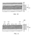
- FIG. 10 is a process cross-sectional view showing the manufacturing method of the EUV mask according to the embodiment.
- FIG. 11 is a cross-sectional view showing the EUV mask manufactured in the embodiment.
- an acceptance determining method of a blank for an EUV mask includes evaluating whether or not an integrated circuit device becomes defective, on the basis of information of a defect contained in a blank for an EUV mask and design information of a mask pattern to be formed on the blank.
- the integrated circuit device is to be manufactured by using the EUV mask.
- the EUV mask is manufactured by forming the mask pattern on the blank.
- the blank is determined to be non-defective in a case that the integrated circuit device is not to be defective.
- the embodiment is an embodiment of an acceptance determining method of a blank for EUV mask and a manufacturing method of an EUV mask.
- FIG. 1 is a plan view showing a blank for EUV mask which is an object of the acceptance determining method according to the embodiment
- FIG. 2 is a cross-sectional view showing the blank for EUV mask which is an object of the acceptance determining method according to the embodiment.
- a quartz substrate 101 is provided.
- the quartz substrate 101 has a substantially rectangular-solid plate shape.
- a multilayer film 102 is provided on the quartz substrate 101 .
- a molybdenum (Mo) layer 103 and a silicon (Si) layer 104 are alternately laminated in several tens of layers.
- the multilayer film 102 functions as a reflection film for EUV light.
- the number of laminations of the molybdenum layer 103 and the silicon layer 104 is expressed smaller than actuality for convenience of Illustration.
- the shape of the blank 100 is a rectangle, and a mask pattern formation region 106 is set at the center part
- the mask pattern formation region 106 is a region where an absorption film which absorbs EUV light is selectively provided on the multilayer film 102 , and a mask pattern 210 (See FIG. 11 ) is formed when the EUV mask is to be manufactured by using the blank 100 .
- a periphery part of the blank 100 that is, a frame-shaped region surrounding the mask pattern formation region 106 is a peripheral region 107 . At two regions sandwiching the mask pattern formation region 106 in the peripheral region 107 , position-referring marks 108 are formed. As will be described later, by forming the mask pattern 210 (See FIG.
- the EUV mask 200 (See FIG. 11 ) on the mask pattern formation region 106 of the blank 100 , the EUV mask 200 (See FIG. 11 ) is manufactured. Also, by performing EUV exposure by using this EUV mask 200 , an integrated circuit device 300 (See FIG. 7 ) such as a memory device is manufactured. In the embodiment, the integrated circuit device 300 is assumed to be a device having a redundancy circuit.
- defects 110 a , 110 b , and 110 c of the blank 100 are schematically illustrated.
- a particle 111 a is interposed between the quartz substrate 101 and the multilayer film 102 .
- the molybdenum layer 103 and the silicon layer 104 laminated in the lower part of the multilayer film 102 a portion located immediately above the particle 111 a and the periphery thereof are raised.
- the portions immediately above the particle 111 a and the periphery thereof in the lower part of the multilayer film 102 has the laminated film thicknesses of the molybdenum layer 103 and the silicon layer 104 varied with respect to the other portions in the multilayer film 102 .
- the degree of raising of the molybdenum layer 103 and the silicon layer 104 becomes smaller as it gets closer to an upper face 102 a of the multilayer film 102 , and the upper face 102 a is not substantially raised.
- a particle 111 b is present inside the multilayer film 102 .
- the molybdenum layer 103 and the silicon layer 104 are raised.
- the degree of raising also becomes smaller as it gets closer to the upper face 102 a of the multilayer film 102 , but the raising does not disappear completely even on the upper face 102 a but the portion immediately above the particle 111 b and the periphery thereof on the upper face 102 a are raised with respect to the other regions.
- a particle 111 c adheres to the upper face 102 a of the multilayer film 102 .
- no defect is present in the lamination structure of the molybdenum layer 103 and the silicon layer 104 .
- the particles 111 a , 111 b , and 111 c are particles that had been present in the atmosphere which mixed in during film formation of the multilayer film 102 , for example.
- the defect 110 a does not cause a defect in a mask pattern (hereinafter referred to as a “pattern defect”).
- the thicknesses of the molybdenum layer 103 and the silicon layer 104 are varied, in reflection light when the multilayer film 102 is irradiated with the EUV light, a phase difference involved with the local fluctuation of the reflectivity of the EUV light is generated between the portion corresponding to the defect 110 a and the periphery thereof.
- phase defect For example, assuming that the EUV light has the wavelength of 13.5 nm and an incident angle when the EUV light enters the mask is 5.8 degrees, with a shift of the lamination film thickness only by approximately 3.5 nm, a phase difference of ⁇ is generated As a result, strength of the portion corresponding to the defect 110 a in the reflection light is extremely lowered, which becomes a dark part. Such a defect is called a “phase defect”.
- the defect 110 b since the upper face 102 a of the multilayer film 102 is raised by reflecting the shape of the particle 111 b , it makes an obstacle when a mask pattern is formed. That is, it can cause a pattern defect.
- a defect in the blank that can cause a pattern defect when a mask pattern is formed as above will be referred to as a “pattern disturbing defect.”
- the defect 110 b since the lamination film thickness is varied, the defect 110 b is also a phase defect.
- the defect 110 c since the lamination film thickness is not varied, this is not a phase defect. However, since the particle 111 c adhering to the upper face 102 a of the multilayer film 102 becomes an obstacle when a mask pattern is formed, it can cause a pattern defect. Therefore, the defect 110 c is a pattern disturbing defect.
- defects might have occurred in the blank 100 .
- Such defects are detected by inspecting the blank 100 For example, by emitting light for inspection to the blank 100 , by measuring intensity of the reflection light, and by preparing a spatial profile, defects in the blank 100 can be detected.
- defects in the blank 100 can be detected.
- irregularity on the upper face 102 a of the multilayer film 102 can be detected, and a pattern disturbing defect can be detected.
- ultraviolet ray other than the EUV light (extreme ultraviolet ray) as the light for inspection a pattern disturbing defect and a part of phase defects can be detected.
- the defect information is primary data such as a spatial profile of the intensity of the reflection light or a spatial profile of contrast obtained by removing a background from the intensity of the reflection light and the like, for example, or secondary data such as a position, size and the like of each defect calculated from the primary data. Coordinates of the data can be outputted by using the position referring marks 108 as references.
- the method of determining acceptance of the blank for EUV mask according to the embodiment is a method of determining whether the blank 100 is “non-defective” or “defective”.
- FIG. 3 is a flowchart showing a method of determining acceptance of the blank for EUV mask according to the embodiment
- FIGS. 4A and 4B are diagrams showing an effect of a phase defect of the blank on acceptance of an integrated circuit device
- FIGS. 5A and 5B are diagrams showing an effect of a pattern disturbing defect of the blank on acceptance of the integrated circuit device
- FIGS. 6A and 6B are diagrams showing an effect of a pattern disturbing defect of the blank on acceptance of the integrated circuit device
- FIG. 7 is a plan view showing the integrated circuit device having a redundancy circuit
- FIG. 8 is a plan view showing the redundancy circuit of the integrated circuit device.
- FIG. 9 is a flowchart showing a method of determining whether or not a remedy by the redundancy circuit is possible.
- Step S 1 in FIG. 3 defect information on the blank 100 to be determined is obtained.
- Step S 2 the obtained defect information is referred to, and it is checked whether or not a defect is present in this blank 100 . If a defect is not present, the routine proceeds to Step S 9 , and it is determined that this blank 100 is “non-defective”. On the other hand, if there is a defect, the routine proceeds to Step S 3 , and more detailed evaluation is made on the defect.
- Step S 3 on the basis of the defect information of the defect contained in the blank 100 and design information of a mask pattern to be formed on this blank 100 , it is determined whether this defect is a “killer defect” or not.
- the design information of the mask pattern is information on the shape of an absorption film to be selectively formed on the blank 100 or information corresponding to a layout and a dimension or the like of wiring of the integrated circuit device 300 to be manufactured, for example.
- the killer defect is a defect which would make this integrated circuit device defective due to the presence of this defect when the EUV mask is fabricated by forming a mask pattern on this blank 100 and the integrated circuit device is manufactured by using this EUV mask.
- Whether or not the defect present in the blank 100 is a killer defect can be determined by simulating an effect of the defect in the blank 100 on the exposed image obtained by irradiating the EUV mask with the EUV light on the basis of the design information of the mask pattern, the lamination structure of the EUV mask, and the exposure conditions of the EUV exposure, for example.
- the lamination structure of the EUV mask refers to, as illustrated in FIG. 2 , the material, thickness, the number of laminations of each layer forming the multilayer film 102 and the like.
- the exposure conditions of the EUV exposure include parameters indicating characteristics of each material forming the EUV mask, the wavelength of the exposure light (EUV light), illumination conditions, numerical aperture (NA) of the projection optical system, the exposure amount, focus, flare amount, incident angle of the EUV light, and diffusion coefficient of the resist material and the like.
- the exposed image is a projected image formed on an exposure object such as a resist film, for example.
- FIGS. 4A , 4 B, 5 A, 5 B, 6 A, and 6 B illustrate the blank 100 containing a defect, the EUV mask 200 manufactured by forming a mask pattern on this blank 100 , and the integrated circuit device 300 manufactured by using this EUV mask 200 in the order from the left side in the figure, respectively. Also, FIGS. 4A , 5 A, and 6 A illustrate cases in which the integrated circuit device 300 is defective, and FIGS. 4B , 5 B, and 6 B illustrate cases in which the integrated circuit device 300 is non-defective, respectively.
- phase defect 121 in the blank 100 .
- the phase defect 121 is present.
- the mask pattern 210 is formed in the EUV mask 200 .
- the mask pattern 210 is a region where the EUV light is absorbed.
- EUV exposure is performed, and the integrated circuit device 300 is manufactured.
- wiring 301 is assumed to be formed in the region to which the mask pattern 210 in the integrated circuit device 300 was transferred.
- the phase defect 121 of the EUV mask 200 becomes a dark part in the exposed image and acts so that the wiring 301 is expanded.
- the integrated circuit device 300 is determined to be defective.
- the phase defect 121 of the blank 100 is a killer defect. If the distance L becomes zero, the wirings 301 are short-circuited with each other. In this case, too, the integrated circuit device 300 is determined as defective, and thus, the phase defect 121 is a killer defect.
- the integrated circuit device 300 is determined to be non-defective. In this case, the phase defect 121 of the blank 100 is not a killer defect.
- FIGS. 5A and 5B consider a case in which a pattern disturbing defect 122 is present in the blank 100 .
- a pattern defect 222 occurs in the EUV mask 200 manufactured by using this blank 100 .
- This pattern defect 222 is assumed to be a non-transparent defect which shuts out the EUV light.
- the integrated circuit device 300 if the distance L between the wirings 301 becomes less than the allowable value due to the pattern defect 222 of the EUV mask 200 , the integrated circuit device 300 is determined to be defective. In this case, the pattern disturbing defect 122 of the blank 100 is a killer defect. If the distance L becomes zero, the wirings 301 are short-circuited with each other and the integrated circuit device 300 is determined as defective, and thus, the pattern disturbing defect 122 is a killer defect.
- the integrated circuit device 300 is determined to be non-defective. In this case, the pattern disturbing defect 122 of the blank 100 is not a killer defect.
- FIGS. 6A and 6B consider a case in which a pattern disturbing defect 123 is present in the blank 100 .
- a pattern defect 223 occurs in the EUV mask 200 manufactured by using this blank 100 .
- This pattern defect 223 is assumed to be a transparent defect which transmits the EUV light.
- the integrated circuit device 300 if a width W of the wiring 301 becomes less than an allowable value due to the pattern defect 223 of the EUV mask 200 , the integrated circuit device 300 is determined to be defective. In this case, the pattern disturbing defect 123 of the blank 100 is a killer defect. If the width W becomes zero, the wiring 301 becomes open, and the integrated circuit device 300 is determined as defective, and thus, the pattern disturbing defect 123 is a killer defect.
- the pattern defect 223 is overlapped with a reflection region between the mask patterns 210 , that is, a region where the multilayer film 102 is exposed, and if the width W of the wiring 301 does not become less than the allowable value due to the pattern defect 223 , the integrated circuit device 300 is determined to be non-defective In this case, the pattern disturbing defect 123 of the blank 100 is not a killer defect.
- Step S 3 it is determined whether or not each defect having occurred in the blank 100 is a killer defect.
- Step S 4 if it is not that all the defects present in the blank 100 are killer defects but there is no killer defect in the blank 100 , that is, if the integrated circuit device 300 does not become defective due to the defect of the blank 100 , the routine proceeds to Step S 9 , and this blank 100 is determined to be “non-defective”. On the other hand, if the integrated circuit device 300 becomes defective due to the defect in the blank 100 , that is, if there is one or more killer defects in the blank 100 , the routine proceeds to Step S 5 , and probability to remedy this blank 100 is examined.
- Step S 5 with regard to the blank 100 determined at Step S 4 to make the integrated circuit device 300 defective, whether or not the remedy of this blank 100 is possible by shifting a formation position of the mask pattern with respect to the blank 100 is examined. Specifically, by shifting the formation position of the mask pattern on the basis of the design information of the mask pattern, it is determined whether or not the integrated circuit device 300 is non-defective.
- the blank 100 illustrated in FIGS. 4A , 5 A or 6 A is a blank containing a killer defect.
- the integrated circuit device 300 becomes defective.
- a relative positional relationship between the defect and the mask pattern 210 is changed.
- the defect is no longer a killer defect, and it is likely that the integrated circuit device 300 becomes non-defective.
- Step S 6 by shifting the formation position of the mask pattern with respect to the blank 100 , if the integrated circuit device 300 is non-defective, that is, if it is possible to remedy the blank 100 , the routine proceeds to Step S 9 , and this blank 100 is determined as “non-defective.” On the other hand, if the integrated circuit device 300 does not become non-defective by shifting the formation position of the mask pattern and the blank 100 cannot be remedied, the routine proceeds to Step S 7 , and probability of remedy of the blank 100 by another method is further examined.
- Step S 7 with regard to the blank 100 determined at Step S 6 that it cannot be remedied by shifting the formation position of the mask pattern, probability of remedy by the redundancy circuit of the integrated circuit device 300 is examined.
- the method of this examination will be described below in detail by citing a specific example of the integrated circuit device 300 .
- the integrated circuit device 300 is a semiconductor memory device, for example.
- a semiconductor substrate 310 is provided.
- a word line direction and a bit line direction are set.
- a pad region 311 is provided at one end portion in the bit line direction of the integrated circuit device 300 , and a peripheral circuit region 312 is provided adjacent to that.
- a plurality of sense amplifier regions 313 are provided, and further adjacent to each of the sense amplifier regions 313 , a memory cell region 314 is provided.
- the pad region 311 , the peripheral circuit region 312 , the sense amplifier region 313 , and the memory cell region 314 are arranged in this order along the bit line direction.
- row decoder regions 315 are provided on both sides in the word line direction of each memory cell region 314 . That is, the memory cell regions 314 and the row decoder regions 315 are arranged along the word line direction.
- the memory cell region 314 is a region in which a plurality of memory cells as basic units are integrated and the memory cells are compatible with each other.
- the memory cell region 314 is a region where remedy by the redundancy circuit is possible. Such a region in which remedy by the redundancy circuit is possible will be referred to as an “R/D region” below.
- a memory cell group 321 a to be originally used and a spare memory cell group 321 b as a redundancy circuit are provided in the memory cell region 314 . If a defect 320 occurs in the memory cell belonging to the memory cell group 321 a , use of an entire memory cell row 322 a to which this memory cell belongs is prohibited, and instead, a memory cell row 322 b provided in the memory cell group 321 b is used. As a result, the integrated circuit device 300 is remedied.
- the row decoder region 315 is also a region in which a plurality of compatible basic units are integrated, it is an R/D region in which remedy by the redundancy circuit is possible.
- a redundancy circuit is not provided on the pad region 311 , the peripheral circuit region 312 , and the sense amplifier region 313 , and thus, they are regions in which remedy by the redundancy circuit is not possible. That is, these regions are not the R/D regions.
- Step S 21 in FIG. 9 in the integrated circuit device 300 , it is determined whether or not a position where a defect in the blank 100 is transferred is within an R/D region. In an example illustrated in FIG. 7 , it is determined whether the position of the defect is within the memory cell region 314 or within the row decoder region 315 . If all the defects caused by the defect in the blank 100 are within the R/D region, that is, within the memory cell region 314 or within the row decoder region 315 , the routine proceeds to Step S 22 .
- the routine goes to Step S 24 , and it is determined that remedy of the integrated circuit device 300 by the redundancy circuit is not possible.
- Step S 22 it is determined whether or not the number of the defects transferred into the R/D region is not more than the number capable of being remedied by the redundancy circuit.
- the integrated circuit device 300 having the redundancy circuit has an upper limit on the number of defects that can be remedied by the redundancy circuit. For example, in the example illustrated in FIG. 8 , since the number of the memory cell rows belonging to the memory cell group 321 b , which is a redundancy circuit, is limited, the number of defects that can be remedied by applying the redundancy circuit is also limited.
- the upper limit of the number of defects that can be remedied depends not only on the size of the memory cell group 321 b but also on the arrangement of the defects.
- Step S 23 If the number of defects transferred into the R/D region is not more than the number that can be remedied by the redundancy circuit, the routine proceeds to Step S 23 , and it is determined that the integrated circuit device 300 can be remedied by the redundancy circuit. On the other hand, if the number of defects transferred into the R/D region is larger than the number that can be remedied by the redundancy circuit, the routine proceeds to Step S 24 , and it is determined that the integrated circuit device 300 cannot be remedied by the redundancy circuit.
- Step S 7 illustrated in FIG. 3 if the position where the defect of the blank 100 in the integrated circuit device 300 is transferred is within the R/D region and also, the number of defects is not more than the number that can be remedied, it is determined that the integrated circuit device 300 can be remedied. Whether or not an arbitrary position in the integrated circuit device 300 is within the R/D region can be read out of the design information of the mask pattern, Also, the number of defects that can be remedied by the redundancy circuit can be read out of the design information of the mask pattern.
- Step S 8 in FIG. 3 if the integrated circuit device 300 can be remedied by using the redundancy circuit, the routine proceeds to Step S 9 , and this blank 100 is determined to be “non-defective”. On the other hand, if the integrated circuit device 300 cannot be remedied even by using the redundancy circuit, the routine proceeds to Step S 10 , and this blank 100 is determined to be “defective”.
- this defect is a killer defect (Step S 4 ), it cannot be remedied by shifting the formation position of the mask pattern (Step S 6 ), and it cannot be remedied even by using the redundancy circuit of the integrated circuit device (Step S 8 ), this blank 100 is determined as “defective” (Step S 10 ), while in the other cases, the blank is determined as “non-defective” (Step S 9 ).
- this blank 100 is determined as “defective” (Step S 10 )
- the blank is determined as “non-defective” (Step S 9 ).
- FIG. 10 is a process cross-sectional view showing the manufacturing method of the EUV mask according to the embodiment.
- FIG. 11 is a cross-sectional view showing the EUV mask manufactured in the embodiment.
- the blank 100 determined to be “non-defective” by the acceptance determining method of the blank for EUV mask according to the embodiment is prepared.
- a material which absorbs the EUV light such as tantalum (Ta), for example, is accumulated so as to form an absorption film 151 .
- a resist film 152 exposed to electron beams is formed on the absorption film 151 .
- a resist pattern is formed.
- the absorption film 151 is selectively removed.
- the resist pattern is removed.
- the mask pattern 210 made of the material containing tantalum, for example, is formed on the multilayer film 102 of the blank 100 .
- the EUV mask 200 is manufactured.
- the mask pattern 210 made of the material which absorbs the EUV light is formed on the blank 100 in which the multilayer film 102 is provided on the quartz substrate 101 .
- the resist film (not shown) is formed on a waver (not shown) so as to be used as a material to be worked.
- the resist film may be in contact with the wafer, may be provided on an insulating film provided on the wafer or may be provided on a conductive film provided on the wafer.
- the material to be worked and the EUV mask 200 are set on an EUV exposing machine (not shown).
- an EUV light source of the EUV exposing machine is made to emit the EUV light so as to irradiate the mask pattern formation region 106 (See FIG. 1 ) on the upper face of the EUV mask 200 with the light.
- the EUV light having reached the mask pattern 210 is absorbed by the mask pattern 210 , while the EUV light having passed through the side of the mask pattern 210 and reached the multilayer film 102 is reflected by the multilayer film 102 .
- the EUV light emitted to the EUV mask 200 is selectively reflected, reaches the resist film on the wafer, and forms an exposed image.
- the resist film is locally exposed.
- the material to be worked is taken out of the EUV exposing machine and developed so as to form the resist pattern.
- treatment is applied by using this resist pattern as a mask.
- impurities are selectively implanted by using this resist pattern as a mask so as to form an impurity diffusion layer in the wafer.
- etching is performed by using this resist pattern as a mask and the insulating film or the conductive film provided on the wafer is selectively removed so as to form a contact hole, wiring or the like.
- the integrated circuit device 300 is manufactured. At this time, at least a part of defects contained in the blank 100 becomes a defect of the EUV mask 200 , but the integrated circuit device 300 does not become defective due to the defect in the blank 100 .
- Step S 2 in FIG. 3 with regard to the blank for which presence of a defect is confirmed, it is determined in a process illustrated at Steps S 3 and S 4 whether or not this defect is a killer defect, and if it is not a killer defect, this blank is determined to be “non-defective” as illustrated at Step S 9 . Also, even if the defect in the blank is a killer defect, it is determined in a process illustrated at Steps S 5 and S 6 whether or not remedy is possible by shifting the formation position of the mask pattern, and if the remedy is possible, this blank is determined to be “non-defective”.
- Steps S 7 and S 8 it is determined whether or not the integrated circuit device can be remedied by using the redundancy circuit, and if the remedy is possible, this blank is determined to be “non-defective”. If the EUV mask is manufactured by using the blank determined to be “non-defective” and the integrated circuit device is manufactured by using this EUV mask, the integrated circuit device does not become defective due to the defect in the blank.
- a blank containing a defect is determined as “non-defective” as long as the situation can be avoided in which the integrated circuit device to be manufactured becomes defective, and thus, the yield of the blank can be improved.
- a manufacturing cost of the blank can be reduced, and thus, the manufacturing cost of the EUV mask can be reduced and moreover, the manufacturing cost of the integrated circuit device can be reduced.
- the example is shown in which the evaluation on whether or not the integrated circuit device becomes defective due to a defect in the blank is made by simulating the effect of the defect in the blank on the exposed image, but the invention is not limited by that.
- this evaluation may be made on the basis of experimental data.
- the EUV mask is actually manufactured by using a blank containing a defect, an exposed image is formed by irradiating this EUV mask with the EUV light, the effect of the defect on this exposed image is evaluated, and such experiment results are accumulated in advance. Then, it may be so configured that the effect of the defect contained in the blank to be determined on the exposed image is estimated on the basis of the accumulated experiment results and whether or not the integrated circuit device becomes defective is determined.
- the yield of the blank can be also improved, as compared with the determination of all the blanks containing a defect to be “defective”, by determining at least presence of a killer defect as illustrated at Steps S 3 and S 4 , by determining that the blank is “non-defective” if there is no killer defect, and by determining the blank to be “defective” if there is a killer defect.
- the acceptance determining method of a blank for EUV mask and the manufacturing method of the EUV mask in which the manufacturing cost can be reduced can be realized.
Landscapes
- Physics & Mathematics (AREA)
- Engineering & Computer Science (AREA)
- General Physics & Mathematics (AREA)
- Chemical & Material Sciences (AREA)
- Nanotechnology (AREA)
- Crystallography & Structural Chemistry (AREA)
- Condensed Matter Physics & Semiconductors (AREA)
- Manufacturing & Machinery (AREA)
- Mathematical Physics (AREA)
- Theoretical Computer Science (AREA)
- Preparing Plates And Mask In Photomechanical Process (AREA)
- Exposure Of Semiconductors, Excluding Electron Or Ion Beam Exposure (AREA)
Abstract
Description
Claims (16)
Applications Claiming Priority (2)
| Application Number | Priority Date | Filing Date | Title |
|---|---|---|---|
| JP2011-000100 | 2011-01-04 | ||
| JP2011000100A JP5537443B2 (en) | 2011-01-04 | 2011-01-04 | EUV mask blank quality determination method and EUV mask manufacturing method |
Publications (2)
| Publication Number | Publication Date |
|---|---|
| US20120174045A1 US20120174045A1 (en) | 2012-07-05 |
| US8423926B2 true US8423926B2 (en) | 2013-04-16 |
Family
ID=46381954
Family Applications (1)
| Application Number | Title | Priority Date | Filing Date |
|---|---|---|---|
| US13/237,790 Active US8423926B2 (en) | 2011-01-04 | 2011-09-20 | Acceptance determining method of blank for EUV mask and manufacturing method of EUV mask |
Country Status (4)
| Country | Link |
|---|---|
| US (1) | US8423926B2 (en) |
| JP (1) | JP5537443B2 (en) |
| KR (1) | KR101281398B1 (en) |
| TW (1) | TWI450027B (en) |
Cited By (1)
| Publication number | Priority date | Publication date | Assignee | Title |
|---|---|---|---|---|
| US20150198896A1 (en) * | 2014-01-16 | 2015-07-16 | Nuflare Technology, Inc. | Exposure mask fabrication method, exposure mask fabrication system, and semiconductor device fabrication method |
Families Citing this family (10)
| Publication number | Priority date | Publication date | Assignee | Title |
|---|---|---|---|---|
| KR101791726B1 (en) * | 2011-03-15 | 2017-10-30 | 케이엘에이-텐코 코포레이션 | Method and apparatus for inspecting a reflective lithographic mask blank and improving mask quality |
| US8726202B2 (en) | 2012-04-13 | 2014-05-13 | International Business Machines Corporation | Mitigation of mask defects by pattern shifting |
| JP6021444B2 (en) * | 2012-05-31 | 2016-11-09 | 株式会社東芝 | Charged beam drawing apparatus and drawing data creation apparatus |
| FR2994605B1 (en) * | 2012-08-20 | 2014-08-22 | Commissariat Energie Atomique | METHOD FOR MANUFACTURING EUV MASKS MINIMIZING THE IMPACT OF SUBSTRATE DEFECTS |
| US8884223B2 (en) * | 2012-11-30 | 2014-11-11 | Kla-Tencor Corporation | Methods and apparatus for measurement of relative critical dimensions |
| JP6013930B2 (en) * | 2013-01-22 | 2016-10-25 | ルネサスエレクトロニクス株式会社 | Manufacturing method of semiconductor device |
| TW201430336A (en) * | 2013-01-23 | 2014-08-01 | Huang Tian Xing | Defect detection method, device and system |
| CN103646894B (en) * | 2013-11-29 | 2016-08-17 | 上海华力微电子有限公司 | Defects scanning method based on critical defect correction |
| US20190056651A1 (en) * | 2017-08-21 | 2019-02-21 | Globalfoundries Inc. | Euv patterning using photomask substrate topography |
| DE102023204171B4 (en) * | 2023-05-05 | 2026-02-19 | Carl Zeiss Smt Gmbh | Optical system for a metrology system and metrology system with such an optical system |
Citations (6)
| Publication number | Priority date | Publication date | Assignee | Title |
|---|---|---|---|---|
| JPH11354404A (en) | 1998-06-05 | 1999-12-24 | Hitachi Ltd | Inspection method and inspection apparatus for blanks and reflective mask |
| JP2001033941A (en) | 1999-07-16 | 2001-02-09 | Toshiba Corp | Pattern forming method and exposure apparatus |
| US7005649B1 (en) | 2004-09-13 | 2006-02-28 | Intel Corporation | Mask blanks inspection method and mask blank inspection tool |
| JP2009010373A (en) | 2007-06-20 | 2009-01-15 | Advanced Mask Technology Center Gmbh & Co Kg | EUV mask and method for correcting EUV mask |
| JP2010034600A (en) | 2009-11-16 | 2010-02-12 | Nec Electronics Corp | Method of euv exposure |
| US20110161893A1 (en) * | 2009-12-31 | 2011-06-30 | Taiwan Semiconductor Manufacturing Company, Ltd. | Lithographic plane check for mask processing |
Family Cites Families (10)
| Publication number | Priority date | Publication date | Assignee | Title |
|---|---|---|---|---|
| JP2002100548A (en) * | 2000-09-21 | 2002-04-05 | Hitachi Ltd | Semiconductor device yield prediction system, yield prediction method, and semiconductor device design method |
| TWI229894B (en) * | 2002-09-05 | 2005-03-21 | Toshiba Corp | Mask defect inspecting method, semiconductor device manufacturing method, mask defect inspecting apparatus, generating method of defect influence map, and computer program product |
| JP2004356330A (en) * | 2003-05-28 | 2004-12-16 | Sony Corp | Mask manufacturing method, mask blank management method, mask blank management program, mask blank management apparatus, and semiconductor device manufacturing method |
| JP4660358B2 (en) * | 2005-11-18 | 2011-03-30 | 大日本印刷株式会社 | Board selection device |
| JP2008129477A (en) * | 2006-11-24 | 2008-06-05 | Toshiba Microelectronics Corp | Photomask making apparatus and photomask inspection apparatus |
| JP5039495B2 (en) * | 2007-10-04 | 2012-10-03 | ルネサスエレクトロニクス株式会社 | Mask blank inspection method, reflective exposure mask manufacturing method, reflective exposure method, and semiconductor integrated circuit manufacturing method |
| JP2010060904A (en) * | 2008-09-04 | 2010-03-18 | Toshiba Corp | Photomask inspection method, semiconductor device inspection method, and pattern inspection apparatus |
| JP5874407B2 (en) * | 2012-01-23 | 2016-03-02 | 大日本印刷株式会社 | Method of manufacturing a reflective mask for EUV exposure that reduces the influence of phase defects |
| JP2013229365A (en) * | 2012-04-24 | 2013-11-07 | Toppan Printing Co Ltd | Reflection mask blank, manufacturing method therefor, reflection mask and manufacturing method therefor |
| JP2013251441A (en) * | 2012-06-01 | 2013-12-12 | Toshiba Corp | Method for supplying mask blank simulation information |
-
2011
- 2011-01-04 JP JP2011000100A patent/JP5537443B2/en active Active
- 2011-08-25 TW TW100130567A patent/TWI450027B/en active
- 2011-09-07 KR KR1020110090602A patent/KR101281398B1/en active Active
- 2011-09-20 US US13/237,790 patent/US8423926B2/en active Active
Patent Citations (7)
| Publication number | Priority date | Publication date | Assignee | Title |
|---|---|---|---|---|
| JPH11354404A (en) | 1998-06-05 | 1999-12-24 | Hitachi Ltd | Inspection method and inspection apparatus for blanks and reflective mask |
| JP2001033941A (en) | 1999-07-16 | 2001-02-09 | Toshiba Corp | Pattern forming method and exposure apparatus |
| US6765673B1 (en) * | 1999-07-16 | 2004-07-20 | Kabushiki Kaisha Toshiba | Pattern forming method and light exposure apparatus |
| US7005649B1 (en) | 2004-09-13 | 2006-02-28 | Intel Corporation | Mask blanks inspection method and mask blank inspection tool |
| JP2009010373A (en) | 2007-06-20 | 2009-01-15 | Advanced Mask Technology Center Gmbh & Co Kg | EUV mask and method for correcting EUV mask |
| JP2010034600A (en) | 2009-11-16 | 2010-02-12 | Nec Electronics Corp | Method of euv exposure |
| US20110161893A1 (en) * | 2009-12-31 | 2011-06-30 | Taiwan Semiconductor Manufacturing Company, Ltd. | Lithographic plane check for mask processing |
Non-Patent Citations (1)
| Title |
|---|
| Notification of Comments, issued by Korean Patent Office, mailed Dec. 7, 2012, in Korean Patent App. No. 10-2011-90602 (8 pages including English translation). |
Cited By (2)
| Publication number | Priority date | Publication date | Assignee | Title |
|---|---|---|---|---|
| US20150198896A1 (en) * | 2014-01-16 | 2015-07-16 | Nuflare Technology, Inc. | Exposure mask fabrication method, exposure mask fabrication system, and semiconductor device fabrication method |
| US9406573B2 (en) * | 2014-01-16 | 2016-08-02 | Nuflare Technology, Inc. | Exposure mask fabrication method, exposure mask fabrication system, and semiconductor device fabrication method |
Also Published As
| Publication number | Publication date |
|---|---|
| TW201229656A (en) | 2012-07-16 |
| JP5537443B2 (en) | 2014-07-02 |
| KR101281398B1 (en) | 2013-07-02 |
| KR20120081921A (en) | 2012-07-20 |
| JP2012142468A (en) | 2012-07-26 |
| TWI450027B (en) | 2014-08-21 |
| US20120174045A1 (en) | 2012-07-05 |
Similar Documents
| Publication | Publication Date | Title |
|---|---|---|
| US8423926B2 (en) | Acceptance determining method of blank for EUV mask and manufacturing method of EUV mask | |
| TW594869B (en) | Manufacturing method of photomask and photomask | |
| JP5155017B2 (en) | Manufacturing method of semiconductor integrated circuit device | |
| US8592102B2 (en) | Cost-effective method for extreme ultraviolet (EUV) mask production | |
| JP2010206177A (en) | Exposure mask, method for manufacturing same, and method for manufacturing semiconductor device | |
| JP2014143239A (en) | Method of manufacturing semiconductor device | |
| US9329472B2 (en) | Method for manufacturing EUV masks minimizing the impact of substrate defects | |
| JP2013222811A (en) | Euv mask blanks, mask manufacturing method, and alignment method | |
| JP5356114B2 (en) | Exposure mask and method of manufacturing semiconductor device | |
| US7735055B2 (en) | Method of creating photo mask data, method of photo mask manufacturing, and method of manufacturing semiconductor device | |
| US9739723B1 (en) | Methods of defect inspection for photomasks | |
| KR101569896B1 (en) | Reflective type photomask and manufacturing method thereof | |
| JP2012089580A (en) | Method of manufacturing mask for euvl and method of manufacturing semiconductor | |
| US9116433B2 (en) | Double-mask photolithography method minimizing the impact of substrate defects | |
| JP2013026424A (en) | Manufacturing method of semiconductor device | |
| JP2012064770A (en) | Method of manufacturing mask for euvl and method of manufacturing semiconductor device | |
| US9274411B2 (en) | Reflection type blank masks, methods of fabricating the same, and methods of fabricating reflection type photo masks using the same | |
| JP5111205B2 (en) | REFLECTIVE MASK, ITS INSPECTION METHOD, AND SEMICONDUCTOR DEVICE MANUFACTURING METHOD | |
| US8748065B2 (en) | Reflection type blank masks, methods of fabricating the same, and methods of fabricating reflection type photo masks using the same | |
| JP2013093588A (en) | Manufacturing method of reflective mask and manufacturing method of semiconductor integrated circuit device | |
| US12055861B2 (en) | Inspection method, inspection system, and semiconductor fabrication using the same | |
| JP2008047598A (en) | Manufacturing method of semiconductor device | |
| JP2004226444A (en) | Method for manufacturing mask and method for manufacturing semiconductor integrated circuit device |
Legal Events
| Date | Code | Title | Description |
|---|---|---|---|
| AS | Assignment |
Owner name: KABUSHIKI KAISHA TOSHIBA, JAPAN Free format text: ASSIGNMENT OF ASSIGNORS INTEREST;ASSIGNORS:KOSHIBA, TAKESHI;MUKAI, HIDEFUMI;MIYOSHI, SEIRO;AND OTHERS;REEL/FRAME:027301/0875 Effective date: 20110930 |
|
| STCF | Information on status: patent grant |
Free format text: PATENTED CASE |
|
| FPAY | Fee payment |
Year of fee payment: 4 |
|
| AS | Assignment |
Owner name: TOSHIBA MEMORY CORPORATION, JAPAN Free format text: ASSIGNMENT OF ASSIGNORS INTEREST;ASSIGNOR:KABUSHIKI KAISHA TOSHIBA;REEL/FRAME:043709/0035 Effective date: 20170706 |
|
| MAFP | Maintenance fee payment |
Free format text: PAYMENT OF MAINTENANCE FEE, 8TH YEAR, LARGE ENTITY (ORIGINAL EVENT CODE: M1552); ENTITY STATUS OF PATENT OWNER: LARGE ENTITY Year of fee payment: 8 |
|
| AS | Assignment |
Owner name: K.K. PANGEA, JAPAN Free format text: MERGER;ASSIGNOR:TOSHIBA MEMORY CORPORATION;REEL/FRAME:055659/0471 Effective date: 20180801 Owner name: TOSHIBA MEMORY CORPORATION, JAPAN Free format text: CHANGE OF NAME AND ADDRESS;ASSIGNOR:K.K. PANGEA;REEL/FRAME:055669/0401 Effective date: 20180801 Owner name: KIOXIA CORPORATION, JAPAN Free format text: CHANGE OF NAME AND ADDRESS;ASSIGNOR:TOSHIBA MEMORY CORPORATION;REEL/FRAME:055669/0001 Effective date: 20191001 |
|
| MAFP | Maintenance fee payment |
Free format text: PAYMENT OF MAINTENANCE FEE, 12TH YEAR, LARGE ENTITY (ORIGINAL EVENT CODE: M1553); ENTITY STATUS OF PATENT OWNER: LARGE ENTITY Year of fee payment: 12 |