US8410856B2 - Method and apparatus for canceling balun amplifier noise - Google Patents
Method and apparatus for canceling balun amplifier noise Download PDFInfo
- Publication number
- US8410856B2 US8410856B2 US12/971,307 US97130710A US8410856B2 US 8410856 B2 US8410856 B2 US 8410856B2 US 97130710 A US97130710 A US 97130710A US 8410856 B2 US8410856 B2 US 8410856B2
- Authority
- US
- United States
- Prior art keywords
- outputs
- amplifier
- branches
- scaled
- summed
- Prior art date
- Legal status (The legal status is an assumption and is not a legal conclusion. Google has not performed a legal analysis and makes no representation as to the accuracy of the status listed.)
- Active, expires
Links
- 238000000034 method Methods 0.000 title claims description 22
- 239000003990 capacitor Substances 0.000 claims description 7
- 238000004590 computer program Methods 0.000 claims description 4
- 238000013459 approach Methods 0.000 description 51
- 238000010586 diagram Methods 0.000 description 22
- 230000006870 function Effects 0.000 description 9
- 230000008569 process Effects 0.000 description 7
- 238000012546 transfer Methods 0.000 description 7
- 238000013461 design Methods 0.000 description 5
- 238000004891 communication Methods 0.000 description 4
- 230000006872 improvement Effects 0.000 description 4
- 238000012545 processing Methods 0.000 description 4
- 230000008901 benefit Effects 0.000 description 3
- 238000001193 catalytic steam reforming Methods 0.000 description 3
- 230000010363 phase shift Effects 0.000 description 3
- 238000003491 array Methods 0.000 description 2
- 230000015556 catabolic process Effects 0.000 description 2
- 230000008859 change Effects 0.000 description 2
- 238000006731 degradation reaction Methods 0.000 description 2
- 239000000463 material Substances 0.000 description 2
- 238000012986 modification Methods 0.000 description 2
- 230000004048 modification Effects 0.000 description 2
- 230000003321 amplification Effects 0.000 description 1
- 238000006243 chemical reaction Methods 0.000 description 1
- 230000001149 cognitive effect Effects 0.000 description 1
- 238000006880 cross-coupling reaction Methods 0.000 description 1
- 230000003247 decreasing effect Effects 0.000 description 1
- 230000000694 effects Effects 0.000 description 1
- 230000003993 interaction Effects 0.000 description 1
- 230000007246 mechanism Effects 0.000 description 1
- 238000003199 nucleic acid amplification method Methods 0.000 description 1
- 230000003287 optical effect Effects 0.000 description 1
- 230000011664 signaling Effects 0.000 description 1
- 238000001228 spectrum Methods 0.000 description 1
- 230000003068 static effect Effects 0.000 description 1
- 239000000758 substrate Substances 0.000 description 1
Images


Classifications
-
- H—ELECTRICITY
- H03—ELECTRONIC CIRCUITRY
- H03F—AMPLIFIERS
- H03F3/00—Amplifiers with only discharge tubes or only semiconductor devices as amplifying elements
- H03F3/189—High-frequency amplifiers, e.g. radio frequency amplifiers
- H03F3/19—High-frequency amplifiers, e.g. radio frequency amplifiers with semiconductor devices only
- H03F3/193—High-frequency amplifiers, e.g. radio frequency amplifiers with semiconductor devices only with field-effect devices
-
- H—ELECTRICITY
- H03—ELECTRONIC CIRCUITRY
- H03F—AMPLIFIERS
- H03F1/00—Details of amplifiers with only discharge tubes, only semiconductor devices or only unspecified devices as amplifying elements
- H03F1/32—Modifications of amplifiers to reduce non-linear distortion
- H03F1/3205—Modifications of amplifiers to reduce non-linear distortion in field-effect transistor amplifiers
-
- H—ELECTRICITY
- H03—ELECTRONIC CIRCUITRY
- H03F—AMPLIFIERS
- H03F3/00—Amplifiers with only discharge tubes or only semiconductor devices as amplifying elements
- H03F3/45—Differential amplifiers
- H03F3/45071—Differential amplifiers with semiconductor devices only
- H03F3/45076—Differential amplifiers with semiconductor devices only characterised by the way of implementation of the active amplifying circuit in the differential amplifier
- H03F3/45179—Differential amplifiers with semiconductor devices only characterised by the way of implementation of the active amplifying circuit in the differential amplifier using MOSFET transistors as the active amplifying circuit
-
- H—ELECTRICITY
- H03—ELECTRONIC CIRCUITRY
- H03F—AMPLIFIERS
- H03F2200/00—Indexing scheme relating to amplifiers
- H03F2200/09—A balun, i.e. balanced to or from unbalanced converter, being present at the output of an amplifier
-
- H—ELECTRICITY
- H03—ELECTRONIC CIRCUITRY
- H03F—AMPLIFIERS
- H03F2200/00—Indexing scheme relating to amplifiers
- H03F2200/294—Indexing scheme relating to amplifiers the amplifier being a low noise amplifier [LNA]
-
- H—ELECTRICITY
- H03—ELECTRONIC CIRCUITRY
- H03F—AMPLIFIERS
- H03F2200/00—Indexing scheme relating to amplifiers
- H03F2200/451—Indexing scheme relating to amplifiers the amplifier being a radio frequency amplifier
-
- H—ELECTRICITY
- H03—ELECTRONIC CIRCUITRY
- H03F—AMPLIFIERS
- H03F2200/00—Indexing scheme relating to amplifiers
- H03F2200/456—A scaled replica of a transistor being present in an amplifier
-
- H—ELECTRICITY
- H03—ELECTRONIC CIRCUITRY
- H03F—AMPLIFIERS
- H03F2200/00—Indexing scheme relating to amplifiers
- H03F2200/462—Indexing scheme relating to amplifiers the current being sensed
-
- H—ELECTRICITY
- H03—ELECTRONIC CIRCUITRY
- H03F—AMPLIFIERS
- H03F2200/00—Indexing scheme relating to amplifiers
- H03F2200/471—Indexing scheme relating to amplifiers the voltage being sensed
-
- H—ELECTRICITY
- H03—ELECTRONIC CIRCUITRY
- H03F—AMPLIFIERS
- H03F2200/00—Indexing scheme relating to amplifiers
- H03F2200/492—A coil being added in the source circuit of a transistor amplifier stage as degenerating element
-
- H—ELECTRICITY
- H03—ELECTRONIC CIRCUITRY
- H03F—AMPLIFIERS
- H03F2203/00—Indexing scheme relating to amplifiers with only discharge tubes or only semiconductor devices as amplifying elements covered by H03F3/00
- H03F2203/45—Indexing scheme relating to differential amplifiers
- H03F2203/45318—Indexing scheme relating to differential amplifiers the AAC comprising a cross coupling circuit, e.g. two extra transistors cross coupled
Definitions
- LNA low-noise amplifier
- the desired frequency span can be processed by one LNA circuit or by several LNA circuits each for processing a smaller band.
- a single-ended LNA is efficient because antennas and RF filters usually produce single ended signals, and conserves area, power, and costs.
- differential signaling in the receive chain reduces second-order distortion and rejects power supply and substrate noise.
- a balun may be used to convert the single-ended RF signal into a differential signal.
- a single-input differential-output low-noise on-chip amplifier i.e., a balun LNA
- a balun is a type of electrical transformer that converts electrical differential signals balanced about ground to unbalanced (single-ended) signals and vice versa.
- a low-noise amplifier (LNA) is an electronic amplifier used to amplify very weak signals (for example, captured by an antenna).
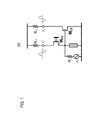
- FIG. 1 is a block diagram depicting an example of a single-stage balun LNA composed by common-gate (CG) common-source (CS) amplifiers.
- CG common-gate
- CS common-source
- FIG. 2 is a simplified schematic of the CG-CS balun amplifier to show the noise transfer functions of FIG. 1 .
- a common-gate amplifier is typically used as a current amplifier, while a common-source amplifier is typically used as a voltage or transconductance amplifier.
- the common-gate (CG) amplifier as shown in FIG. 2 is applied for its wideband impedance match.
- the problems of a noise figure (NF) greater than 3.5 dB and an insufficient voltage gain are alleviated by the parallel common-source (CS) amplifier.
- CS parallel common-source
- Noise figure is a measure of degradation of the signal-to-noise ratio (SNR), caused by components in a radio frequency (RF) signal chain.
- the noise figure is defined as the ratio of the output noise power of a device to the portion thereof attributable to thermal noise in the input termination at standard noise temperature T 0 (usually 290 K).
- the noise/distortion from M CG (M 1 ) is canceled by taking the output differentially.
- the M CS (M 2 ) noise dominates the NF.
- the parallel CS amplifier doubles the voltage gain and cancels the noise and distortions generated from the CG amplifier.
- the CG-CS input stage also naturally performs single-to-differential conversion, which may be provided a low-cost implementation without an extra off-chip balun.
- g m,CG and g m,CS respectively represent the transconductance of the CG and CS amplifiers.
- Transconductance (g m ), also known as mutual conductance, is the ratio of the current change at the output port to the voltage change at the input port.
- R L1 and R L2 respectively represent the resistor loads of the CG and CS branches. Rs is the source resistance and equal to 50 ohm.
- T i,CG and T i,CS respectively denote the current transfer gains in the differential outputs due to the CG and CS transistor noise currents, i.e., i n,M1 and i n,M2 are respectively shown as follows:
- T i,Rs represents the transfer gain in the differential output due to the Rs noise current, i.e., i n,Rs .
- CG transistor channel noise i n,CG results in the noise currents i nd1 and i nd2 at the drain ports of the CG and CS amplifiers, respectively, and T i,CG is the difference of these two components normalized to i n,CG .
- T i,CG denotes the current transfer gain in the differential output due to the CG transistor noise current, i.e., i n,M1 , and can be expressed by:
- T i,CS denotes the current transfer gain in the differential output due to the CS transistor noise current, i.e., i n,M2 , and is equal to one.
- a conventional approach suggested an inductorless LNA and derives conditions for simultaneous output balancing, noise canceling and distortion canceling, by admittance scaling the CS-stage with respect to the CG-stage for noise canceling.
- This approach obtains a noise figure in the order of 3 dB or lower.
- Another conventional approach suggested a feedforward thermal noise-canceling technique for a LNA, which allows for simultaneous noise and impedance matching, while canceling the noise and distortion contributions of the matching device.
- This approach provides wide-band impedance-matching amplifiers with a NF range of 1.9-2.4 dB, without suffering from instability issues.
- a third conventional approach suggested a differential common-gate LNA consisting of cross-coupled capacitors and PMOS transistors in a differential CG configuration.
- the differential common-gate LNA reduces the power consumption to 3.6 mW, yet providing only an average 3 dB NF in the frequency range of 0.3-0.92 GHz.
- a fourth conventional approach suggested a LNA with single-ended input and output employing noise and IM 2 distortion cancellation for a digital terrestrial and cable TV tuner.
- the single-ended LNA adopts thermal noise canceling based on current amplification, to acquire low NF (e.g., 3.0-3.3 dB) and high third-order intercept point (IIP3) performance (e.g., 3 dBm) without degradation of gain and wideband input matching.
- NF3 e.g., 3.0-3.3 dB
- IIP3 third-order intercept point
- TOI is used to measure weakly nonlinear systems and devices (e.g., receivers, linear amplifiers and mixers, etc.). It is assumed that the device nonlinearity can be modeled using a low-order polynomial.
- the third-order intercept point relates nonlinear products caused by the third-order nonlinear term to the linearly amplified signal.
- NF noise figure
- a noise cancelling method is provided to improve the NF, the method which comprises summing and scaling an output from a current-sensing (e.g., common-gate) branch of an amplifier and an output from a voltage sensing (e.g., common-source) branch of the amplifier into one or more summed and scaled outputs.
- the method may also comprise feeding the one or more summed and scaled outputs back to at least one of the outputs of the branches of the amplifier.
- an apparatus which comprises a current sensing amplifier and a voltage sensing amplifier.
- the apparatus may also comprises a control module which sums and scales an output from the current sensing amplifier and an output from the voltage sensing amplifier, wherein the control module feeds one or more summed and scaled outputs back to at least one of the outputs of the current and voltage sensing amplifiers.
- an apparatus which comprises at least one processor; and at least one memory including computer program code for one or more programs.
- the at least one memory and the computer program code may be configured, with the at least one processor, to cause the apparatus to perform at least the following: sum and scale an output from a current-sensing branch of an amplifier and an output from a voltage sensing branch of the amplifier into one or more summed and scaled outputs; and feed the one or more summed and scaled outputs back to at least one of the outputs of the branches of the amplifier.
- FIG. 1 is a block diagram depicting an example of a single-stage balun LNA composed by common-gate (CG) common-source (CS) amplifiers;
- CG common-gate
- CS common-source
- FIG. 2 shows a simulated schematic of the CG-CS balun amplifier of FIG. 1 ;
- FIG. 3 is a block diagram of an exemplary embodiment of a single-stage CG-CS balun amplifier applied with a summing/scaling approach;
- FIG. 4 is a flowchart of an exemplary embodiment of a process for reducing the noise figure of a CG-CS balun LNA without sacrificing the other performance (such as gain, IIP3, and wideband impedance matching);
- FIG. 5 shows an equivalent diagram of feedback gains implemented by the CG-CS balun amplifier of FIG. 3 ;
- FIGS. 6A-6B show a first simulated circuit topology based on the summing and scaling approach, a NF diagram and an IIP3 diagram of the first simulated circuit topology;
- FIGS. 7A-7B show a second simulated circuit topology based on the summing and scaling approach, a NF diagram and an IIP3 diagram of the second simulated circuit topology
- FIGS. 8A-8B show a third simulated circuit topology based on the summing and scaling approach, a NF diagram and an IIP3 diagram of the third simulated circuit topology
- FIG. 9 is a performance comparison table of the simulated circuit topologies and previously discussed wideband LNAs.
- FIG. 10 is a diagram of a chip set that can be used to implement various exemplary embodiments.
- FIG. 11 is a block diagram of a conventional single-ended to differential buffer and a control module applying the summing and scaling approach.
- FIG. 12 is a block diagram of another conventional single-ended to differential LNA and a control module applying the summing and scaling approach.
- FIG. 3 is a block diagram of an exemplary embodiment of a single-stage CG-CS balun amplifier 301 including a control module 303 for applying a summing/scaling approach, in accordance with an exemplary embodiment.
- T i,CS A.
- the noise components at the CS output are reduced and the signal is unchanged.
- the noise components become 0 and k for the CG transistor noise and the CS transistor noise, respectively.
- the noise current gains resulting from the CG and the CS transistor noises, respectively become the same.
- a low k i.e., a higher g m,CG ) leads to a lower NF.
- S 11 is set to be as low as ⁇ 10 dB. This leads to a limit of g m,CG in a range of 11-38 mS. As discussed, a higher g m,CG can result in a better NF. However, to maintain a reasonable S 11 , the g m,CG can be designed as 37 mS, and the corresponding NF range is 1.76 dB as aforementioned.
- FIG. 4 is a flowchart of an exemplary embodiment of a process 400 for reducing the noise figure of a CG-CS balun LNA without sacrificing the other performance (such as gain, IIP3, and wideband impedance matching), in accordance with an exemplary embodiment.
- This process 400 can be performed by a control module 303 of a low noise amplifier in FIG. 3 .
- the control module 303 sums and scales an output from a common-gate branch of the amplifier and an output from a common-source branch of the amplifier into one or more summed and scaled outputs.
- the summing and scaling may include summing the outputs from the branches and then scaling a summed result with a factor, or scaling each of the outputs from the branches with a factor and then summing scaled results.
- the outputs from the branches are summed using one or more inductors, one or more resistors, one or more capacitors, or a combination thereof.
- the outputs from the branches are scaled using two or more common-source amplifiers.
- the control module 303 feeds the one or more summed and scaled outputs back to at least one of the outputs of the branches of the amplifier.
- the feeding back may include feeding back a positive one of the one or more summed and scaled outputs to a positive one of the outputs of the branches of the amplifier, feeding back a negative one of the one or more summed and scaled outputs to a negative one of the outputs of the branches of the amplifier, or a combination thereof.
- a negative one of the outputs of the branches of the amplifier has an inverting phase from an input of the amplifier, and a negatively scaled one of the one or more summed and scaled outputs is fed back to the negative output.
- a positive one of the outputs of the branches of the amplifier has no phase shift from an input of the amplifier, and a positively scaled one of the one or more summed and scaled outputs is fed back to the positive output.
- the first and second embodiments are combined, to feed a negatively scaled one of the one or more summed and scaled outputs back to the negative output, and to feed a positively scaled one of the one or more summed and scaled outputs back to the positive output.
- FIG. 5 illustrates equivalent diagram of feedback gains implemented by the CG-CS balun amplifier of FIG. 3 , in accordance with various exemplary embodiments.
- the CG-CS balun amplifier of FIG. 3 includes a CG (current sensing) amplifier 503 receiving an input signal 501 , a CS (voltage sensing) amplifier 505 receiving the input signal 501 , and a control module.
- CG current sensing
- CS voltage sensing
- control module sums an output 507 from the current sensing amplifier 503 and an output 509 from the voltage sensing amplifier 506 with a summer 511 .
- the control module then scales the summed result with either a factor ⁇ A f using a scaler 513 , a factor +A f using a scaler 515 , or a combination thereof.
- the control module feeds one or more summed and scaled outputs back to at least one of the positive and negative outputs 507 , 509 of the current and sensing voltage amplifiers 503 , 505 .
- the noise figure is reduced significantly.
- the feedback path composed of the summer 511 and the scaler 513 has an inverting phase, i.e., a 180 degree of phase shift from the input 501 .
- the summed component is fed back to the CS branch (negative) output 509 .
- the summed component is fed back to the CG branch (positive) output 507 .
- the feedback path comprises only one scaler/amplifier with a gain ⁇ A f
- the feedback path comprises only one scaler/amplifier with a gain +A f
- a f (1 ⁇ k) and the gain +A f is fed back to the positive output 507 .
- the above-proposed embodiments utilize the summing and scaling approach to reduce the NF of CG-CS balun amplifiers without sacrificing the other performance such as gain, IIP3, and wideband impedance matching.
- g m,CG g m,CS .
- g m,CG is different from g m,CS .
- the proposed summing and scaling approach is still valid, but the design considerations on determining the parameters are slightly different as discussed in conjunction with FIG. 12 .
- the summing and scaling approach can be applied to many types of circuit implementations.
- the following circuit topologies are simulated as examples in FIGS. 6-8 .
- FIG. 6A A first simulated circuit topology 600 based on the summing and scaling approach is shown in FIG. 6A .
- an inductor 601 providing a high-impedance termination where this common-mode termination provides the summed component
- one CS amplifier 603 is used as the scaler.
- one or more resistors, inductors, transistors are applied to implement this summer, and one or more amplifiers other than the CS amplifier are applied to implement this scaler.
- the summed component is coupled to the input of the amplifier and then fed back to the output of the CS branch.
- the CS amplifier 603 is scaled as ⁇ (1 ⁇ k) of the input of the CG-CS amplifier.
- FIG. 6B shows a diagram 620 including simulated NFs of the first circuit topology versus frequency.
- a significant improvement is achieved due to the added feedback circuit based on the summing and scaling approach.
- the simulated NFs 621 based on the summing and scaling approach and the NFs 623 based on the conventional approach depicted in FIG. 1 are shown for comparisons.
- the results show a NF range of 1.5-2.25 dB over 0.1-2 GHz based on the summing and scaling approach, and a NF range of 3.2-3.5 dB over 0.1-2 GHz based on the conventional approach.
- the simulated NFs are 1.25-1.7 dB smaller than those based on the conventional approach.
- the trend of simulated NFs generally aligns with those of the conventional approach over the entire band. Such confirms the effect of broadband noise cancellation as well as the proposed design methodology.
- FIG. 7A The second simulated circuit topology based on the summing and scaling approach is shown in FIG. 7A .
- a pair of capacitors 701 is used as the summer, and one CS amplifier 703 is used as the scaler, where the common-mode termination provides the summed components.
- one or more resistors, inductors, transistors are applied to implement this summer, and one or more amplifiers other than the CS amplifier are applied to implement this scaler.
- the summed components are coupled to the input of the LNA and then feedback to the output of the CS branch.
- FIG. 7B illustrates a diagram 720 including simulated NFs of the second circuit topology versus frequency.
- the simulated NFs 721 based on the summing and scaling approach shows a NF range of 1.75 dB and below 2 dB from 150 MHz to 2 GHz, while the conventional approach has a NF range of 3.2-3.5 dB over 0.1-2 GHz.
- the simulated NFs are 1.15-1.7 dB smaller than those of the conventional approach.
- FIG. 8A The third simulated circuit topology based on the summing and scaling approach is illustrated in FIG. 8A . Different from the first and second topologies, this circuit topology scales the components of two outputs and then sums the scaled components. A pair of CS amplifiers 801 is used to scale feedback factors and then sum the scaled results together at the output of the CS branch.
- FIG. 8B illustrated a diagram 820 including simulated NFs of the third circuit topology versus frequency.
- the simulated NFs 821 based on the summing and scaling approach shows a NF of 1.75 dB and a NF range of below 2 dB from 100 MHz to 1.5 GHz, while the conventional approach has a NF range of 3.2-3.5 dB over 0.1-2 GHz.
- the simulated NFs are 1.15-1.7 dB smaller than those of the conventional approach.
- the third circuit topology sends the output signal directly to the feedback amplifier and introduces additional distortions.
- FIG. 9 is a performance comparison table of the simulated circuit topologies and previously discussed conventional wideband LNAs.
- the simulated performance of LNAs based on the summing and scaling approach is summarized in the Table of FIG. 9 .
- Other previously discussed conventional wideband LNAs are included in the Table for comparisons.
- the proposed summing and scaling approach and circuit topologies benefit from high bandwidth, low average NF over the entire band, and small die area with moderate power consumption.
- the proposed summing and scaling approach and circuit topologies can achieve specific requirements in ultra-low voltage/power (ULVP) microsystems, biomedical applications, wireless sensor networks (WSN), high-speed circuits, etc.
- ULVP ultra-low voltage/power
- the proposed summing and scaling approach and circuit topologies can achieve ultra-low power consumption ( ⁇ 400 ⁇ W, NF ⁇ 4 dB), ultra-low voltage operation ( ⁇ 0.5V), ultra wideband operation (>9 GHz), Balun LNA/fully differential LNA reconfigurability.
- any low noise amplifiers including, but not limited to single-stage CG-CS balun-LNAs.
- Any balun amplifiers composed of a current-sensing amplifier and voltage-sensing amplifier and any balun amplifiers with a post-stage of amplifiers are applicable.
- the processes described herein for reducing the noise figure of a CG-CS balun LNA without sacrificing the other performance may be advantageously implemented via software, hardware, firmware or a combination of software and/or firmware and/or hardware. With this approach, the noise figure of a CG-CS balun LNA is reduced without sacrificing the other performance (such as gain, IIP3, and wideband impedance matching).
- the processes described herein may also be implemented with an Application Specific Integrated Circuit (ASIC), Field Programmable Gate Arrays (FPGAs), etc.
- ASIC Application Specific Integrated Circuit
- FPGAs Field Programmable Gate Arrays
- FIG. 10 is a diagram of a chip set that can be used to implement various exemplary embodiments.
- Chip set 1000 is programmed for reducing the noise figure of a LNA without sacrificing the other performance (such as gain, IIP3, and wideband impedance matching) as described herein and includes, for instance, the processor and memory components incorporated in one or more physical packages (e.g., chips).
- a physical package includes an arrangement of one or more materials, components, and/or wires on a structural assembly (e.g., a baseboard) to provide one or more characteristics such as physical strength, conservation of size, and/or limitation of electrical interaction. It is contemplated that in certain embodiments the chip set 1000 can be implemented in a single chip.
- chip set or chip 1000 can be implemented as a single “system on a chip.” It is further contemplated that in certain embodiments a separate ASIC would not be used, for example, and that all relevant functions as disclosed herein would be performed by a processor or processors. Chip set or chip 1000 , or a portion thereof, performs one or more steps for controlling a direct current gain of a resonant converter to increase power efficiency within a circuit.
- the chip set or chip 1000 includes a communication mechanism such as a bus 1001 for passing information among the components of the chip set 1000 .
- a processor 1003 has connectivity to the bus 1001 to execute instructions and process information stored in, for example, a memory 1005 .
- the processor 1003 may include one or more processing cores with each core configured to perform independently.
- a multi-core processor enables multiprocessing within a single physical package. Examples of a multi-core processor include two, four, eight, or greater numbers of processing cores.
- the processor 1003 may include one or more microprocessors configured in tandem via the bus 1001 to enable independent execution of instructions, pipelining, and multithreading.
- the processor 1003 may also be accompanied with one or more specialized components to perform certain processing functions and tasks such as one or more digital signal processors (DSP) 1007 , or one or more application-specific integrated circuits (ASIC) 1009 .
- DSP digital signal processor
- ASIC application-specific integrated circuits
- a DSP 1007 typically is configured to process real-world signals (e.g., sound) in real time independently of the processor 1003 .
- an ASIC 1009 can be configured to performed specialized functions not easily performed by a more general purpose processor.
- Other specialized components to aid in performing the inventive functions described herein may include one or more field programmable gate arrays (FPGA) (not shown), one or more controllers (not shown), or one or more other special-purpose computer chips.
- FPGA field programmable gate arrays
- the processor 1003 and accompanying components have connectivity to the memory 1005 via the bus 1001 .
- the memory 1005 includes both dynamic memory (e.g., RAM, magnetic disk, writable optical disk, etc.) and static memory (e.g., ROM, CD-ROM, etc.) for storing executable instructions that when executed perform the inventive steps described herein for controlling a direct current gain of a resonant converter to increase power efficiency within a circuit.
- the memory 1005 also stores the data associated with or generated by the execution of the inventive steps.
- FIG. 11 is a block diagram 1100 of a conventional single-ended to differential buffer 1101 and a control module 1103 applying the summing and scaling approach, according to one embodiment.
- the conventional single-ended to differential buffer 1101 uses a pair of common-gate (CG) common-source (CS) amplifiers M 1 , M 2 as an input stage.
- the amplifier utilizes the CG-CS amplifiers as the input stage and generates differential output.
- Two diode-connected MOS transistors M 3 , M 4 are used as the loads to convert the output current into a voltage.
- This topology provides a relatively high linearity yet poor NF.
- the control module 1103 With the addition of the control module 1103 , the NF can be reduced significantly, based on the above-discussed summing and scaling approach and circuit topologies.
- FIG. 12 is a block diagram 1200 of another conventional single-ended to differential LNA 1201 and a control module 1203 applying the summing and scaling approach, according to one embodiment.
- the conventional single-ended to differential LNA 1201 uses the common-gate (CG) common-source (CS) amplifiers as an input stage. It also employs CG-CS amplifiers as the input stage and generates a differential output. Two additional techniques are applied to improve circuit performance such as NF, linearity, and differential balance.
- This current buffer also provides bulk cross-coupling that provides higher gain and lower NF, and enhances g m without introducing extra DC current.
- UUV ultra low voltage
- g m,CS is larger than g m,CG .
- the proposed summing and scaling approach is still valid to effectively reduce NF with careful design parameters.
Landscapes
- Engineering & Computer Science (AREA)
- Power Engineering (AREA)
- Physics & Mathematics (AREA)
- Nonlinear Science (AREA)
- Amplifiers (AREA)
Priority Applications (3)
| Application Number | Priority Date | Filing Date | Title |
|---|---|---|---|
| US12/971,307 US8410856B2 (en) | 2010-12-17 | 2010-12-17 | Method and apparatus for canceling balun amplifier noise |
| TW100106505A TWI399032B (zh) | 2010-12-17 | 2011-02-25 | 消除平衡轉換放大器之雜訊的方法及其裝置 |
| CN201110094569.5A CN102545790B (zh) | 2010-12-17 | 2011-04-07 | 消除平衡-非平衡转换放大器噪声的方法及其装置 |
Applications Claiming Priority (1)
| Application Number | Priority Date | Filing Date | Title |
|---|---|---|---|
| US12/971,307 US8410856B2 (en) | 2010-12-17 | 2010-12-17 | Method and apparatus for canceling balun amplifier noise |
Publications (2)
| Publication Number | Publication Date |
|---|---|
| US20120154056A1 US20120154056A1 (en) | 2012-06-21 |
| US8410856B2 true US8410856B2 (en) | 2013-04-02 |
Family
ID=46233607
Family Applications (1)
| Application Number | Title | Priority Date | Filing Date |
|---|---|---|---|
| US12/971,307 Active 2031-09-29 US8410856B2 (en) | 2010-12-17 | 2010-12-17 | Method and apparatus for canceling balun amplifier noise |
Country Status (3)
| Country | Link |
|---|---|
| US (1) | US8410856B2 (de) |
| CN (1) | CN102545790B (de) |
| TW (1) | TWI399032B (de) |
Cited By (4)
| Publication number | Priority date | Publication date | Assignee | Title |
|---|---|---|---|---|
| US20130257534A1 (en) * | 2012-04-03 | 2013-10-03 | Samsung Electronics Co., Ltd. | Input receiver circuit having single-to-differential amplifier, and semiconductor device including the same |
| WO2015167648A3 (en) * | 2014-02-10 | 2015-12-23 | The Trustees Of Columbia University In The City Of New York | Circuits for reducing out-of-band-modulated transmitter self-interference |
| US20160173145A1 (en) * | 2014-12-16 | 2016-06-16 | Nvidia Corporation | Low noise amplifier providing variable gains and noise cancellation for carrier aggregation |
| US12095424B1 (en) * | 2022-01-06 | 2024-09-17 | National Technology & Engineering Solutions Of Sandia, Llc | Miniature ultra-low-power LNA employing current reuse and bias sharing |
Families Citing this family (5)
| Publication number | Priority date | Publication date | Assignee | Title |
|---|---|---|---|---|
| US9438188B2 (en) * | 2014-09-15 | 2016-09-06 | Qualcomm Incorporated | Common-gate amplifier for high-speed DC-coupling communications |
| EP3139498A1 (de) * | 2015-09-01 | 2017-03-08 | Nokia Technologies Oy | Verfahren und vorrichtung zur verstärkung von signalen |
| CN106803746B (zh) * | 2016-12-14 | 2020-09-04 | 上海集成电路研发中心有限公司 | 一种低噪声放大器 |
| CN109802638B (zh) * | 2018-12-19 | 2023-09-15 | 北京航空航天大学青岛研究院 | 基于全局噪声抵消的低噪声放大器及其方法 |
| CN110957981B (zh) * | 2019-11-28 | 2024-03-15 | 上海磐启微电子有限公司 | 一种增益与阻抗匹配分离的无电感低噪声放大器 |
Citations (14)
| Publication number | Priority date | Publication date | Assignee | Title |
|---|---|---|---|---|
| US4216435A (en) * | 1979-01-25 | 1980-08-05 | Rca Corporation | Voltage-to-current converter apparatus |
| US5404050A (en) | 1992-12-11 | 1995-04-04 | U.S. Philips Corporation | Single-to-differential converter |
| US6271721B1 (en) * | 1999-06-23 | 2001-08-07 | Christopher Trask | Common-base transistor amplifiers with linearity augmentation |
| US6366171B1 (en) | 2000-04-06 | 2002-04-02 | Texas Instruments Incorporated | Single-to-differential low noise amplifier |
| US6542037B2 (en) * | 2001-08-09 | 2003-04-01 | Tyco Electronics Corp. | Low distortion broadband amplifier using GaAs pHEMT devices |
| US6608527B2 (en) | 1999-10-21 | 2003-08-19 | Broadcom Corporation | Adaptive radio transceiver with low noise amplification |
| US6809594B2 (en) | 2002-09-24 | 2004-10-26 | Marvell International, Ltd. | Ultra broadband low noise amplifier with matched reactive input impedance |
| US7378911B2 (en) | 2006-03-16 | 2008-05-27 | Newport Media, Inc. | Wideband ultra low noise amplifier |
| US7671686B2 (en) | 2007-10-24 | 2010-03-02 | Industrial Technology Research Institute | Low noise amplifier |
| US7671685B2 (en) | 2006-12-06 | 2010-03-02 | Broadcom Corporation | Method and system for a low power fully differential noise cancelling low noise amplifier |
| US7737789B2 (en) | 2008-10-19 | 2010-06-15 | University Of Florida Research Foundation, Inc. | Broadband active balun |
| US7777575B2 (en) | 2008-07-17 | 2010-08-17 | Infineon Technologies Ag | Circuit with single-ended input and differential output |
| US7948322B2 (en) * | 2009-09-16 | 2011-05-24 | Industrial Technology Research Institute | Balun amplifier |
| US8138835B2 (en) * | 2010-02-11 | 2012-03-20 | Qualcomm, Incorporated | Wide band LNA with noise canceling |
Family Cites Families (4)
| Publication number | Priority date | Publication date | Assignee | Title |
|---|---|---|---|---|
| US7642816B2 (en) * | 2007-10-10 | 2010-01-05 | Industrial Technology Research Institute | Transconductor |
| US7839219B2 (en) * | 2007-10-24 | 2010-11-23 | Industrial Technology Research Institute | Low-noise amplifier circuit including band-stop filter |
| CN101494441B (zh) * | 2008-01-24 | 2013-04-03 | 三星电子株式会社 | 宽带低噪声放大器 |
| CN101895265A (zh) * | 2010-08-24 | 2010-11-24 | 复旦大学 | 一种全差分cmos多模低噪声放大器 |
-
2010
- 2010-12-17 US US12/971,307 patent/US8410856B2/en active Active
-
2011
- 2011-02-25 TW TW100106505A patent/TWI399032B/zh active
- 2011-04-07 CN CN201110094569.5A patent/CN102545790B/zh active Active
Patent Citations (14)
| Publication number | Priority date | Publication date | Assignee | Title |
|---|---|---|---|---|
| US4216435A (en) * | 1979-01-25 | 1980-08-05 | Rca Corporation | Voltage-to-current converter apparatus |
| US5404050A (en) | 1992-12-11 | 1995-04-04 | U.S. Philips Corporation | Single-to-differential converter |
| US6271721B1 (en) * | 1999-06-23 | 2001-08-07 | Christopher Trask | Common-base transistor amplifiers with linearity augmentation |
| US6608527B2 (en) | 1999-10-21 | 2003-08-19 | Broadcom Corporation | Adaptive radio transceiver with low noise amplification |
| US6366171B1 (en) | 2000-04-06 | 2002-04-02 | Texas Instruments Incorporated | Single-to-differential low noise amplifier |
| US6542037B2 (en) * | 2001-08-09 | 2003-04-01 | Tyco Electronics Corp. | Low distortion broadband amplifier using GaAs pHEMT devices |
| US6809594B2 (en) | 2002-09-24 | 2004-10-26 | Marvell International, Ltd. | Ultra broadband low noise amplifier with matched reactive input impedance |
| US7378911B2 (en) | 2006-03-16 | 2008-05-27 | Newport Media, Inc. | Wideband ultra low noise amplifier |
| US7671685B2 (en) | 2006-12-06 | 2010-03-02 | Broadcom Corporation | Method and system for a low power fully differential noise cancelling low noise amplifier |
| US7671686B2 (en) | 2007-10-24 | 2010-03-02 | Industrial Technology Research Institute | Low noise amplifier |
| US7777575B2 (en) | 2008-07-17 | 2010-08-17 | Infineon Technologies Ag | Circuit with single-ended input and differential output |
| US7737789B2 (en) | 2008-10-19 | 2010-06-15 | University Of Florida Research Foundation, Inc. | Broadband active balun |
| US7948322B2 (en) * | 2009-09-16 | 2011-05-24 | Industrial Technology Research Institute | Balun amplifier |
| US8138835B2 (en) * | 2010-02-11 | 2012-03-20 | Qualcomm, Incorporated | Wide band LNA with noise canceling |
Non-Patent Citations (6)
| Title |
|---|
| Blaakmeer et al., "Wideband Balun-LNA With Simultaneous Output Balancing, Noise-Canceling and Distortion-Canceling", IEEE Journal of Solid-State Circuits, vol. 43, No. 6, Jun. 2008, pp. 1341-1350. |
| Bruccoleri et al., "Wide-Band CMOS Low-Noise Amplifier Exploiting Thermal Noise Canceling", IEEE Journal of Solid-State Circuits, vol. 39, No. 2, Feb. 2004, pp. 275-282. |
| Bult et al., "A Class of Analog CMOS Circuits Based on the Square-Law Characteristic of an MOS Transistor in Saturation", IEEE Journal of Solid-State Circuits, vol. SC-22, No. 3, Jun. 1987, pp. 357-365. |
| Im et al., "A Wideband CMOS Low Noise Amplifier Employing Noise and IM2 Distortion Cancellation for a Digital TV Tuner", IEEE Journal of Solid-State Circuits, vol. 44, No. 3, Mar. 2009, pp. 686-698. |
| Liao et al., "A Broadband Noise-Canceling CMOS LNA for 3.1-10.6-GHz UWB Receivers", IEEE Journal of Solid-State Circuits, vol. 42, No. 2, Feb. 2007, pp. 329-339. |
| Woo et al., "A 3.6mW Differential Common-Gate CMOS LNA with Positive-Negative Feedback", 2009 IEEE International Solid-State Circuits Conference, Feb. 2009, pp. 218-220. |
Cited By (6)
| Publication number | Priority date | Publication date | Assignee | Title |
|---|---|---|---|---|
| US20130257534A1 (en) * | 2012-04-03 | 2013-10-03 | Samsung Electronics Co., Ltd. | Input receiver circuit having single-to-differential amplifier, and semiconductor device including the same |
| US9030262B2 (en) * | 2012-04-03 | 2015-05-12 | Samsung Electronics Co., Ltd. | Input receiver circuit having single-to-differential amplifier, and semiconductor device including the same |
| WO2015167648A3 (en) * | 2014-02-10 | 2015-12-23 | The Trustees Of Columbia University In The City Of New York | Circuits for reducing out-of-band-modulated transmitter self-interference |
| US10454517B2 (en) | 2014-02-10 | 2019-10-22 | The Trustees Of Columbia University In The City Of New York | Circuits for reducing out-of-band-modulated transmitter self-interference |
| US20160173145A1 (en) * | 2014-12-16 | 2016-06-16 | Nvidia Corporation | Low noise amplifier providing variable gains and noise cancellation for carrier aggregation |
| US12095424B1 (en) * | 2022-01-06 | 2024-09-17 | National Technology & Engineering Solutions Of Sandia, Llc | Miniature ultra-low-power LNA employing current reuse and bias sharing |
Also Published As
| Publication number | Publication date |
|---|---|
| US20120154056A1 (en) | 2012-06-21 |
| TW201228217A (en) | 2012-07-01 |
| CN102545790A (zh) | 2012-07-04 |
| CN102545790B (zh) | 2014-09-24 |
| TWI399032B (zh) | 2013-06-11 |
Similar Documents
| Publication | Publication Date | Title |
|---|---|---|
| US8410856B2 (en) | Method and apparatus for canceling balun amplifier noise | |
| US9054648B1 (en) | Wideband active balun LNA topology with narrow-band filtering and noise cancelling | |
| US8872586B2 (en) | Folded-cascode amplifier | |
| CN104579184B (zh) | 一种高线性度宽带巴伦低噪声放大器 | |
| WO2017166109A1 (zh) | 一种低噪声放大器 | |
| CN103534940A (zh) | 正反馈共栅极低噪声放大器 | |
| US20010052815A1 (en) | Noise reduction scheme for operational amplifiers | |
| CN104883135A (zh) | 一种电阻反馈式噪声消除宽带低噪声跨导放大器 | |
| US10326410B2 (en) | Amplifier adapted for noise suppression | |
| CN105281682A (zh) | 低功耗双向降噪低噪声放大器 | |
| Chen et al. | A highly linear wideband CMOS LNTA employing noise/distortion cancellation and gain compensation | |
| Chiang et al. | A 90 nm CMOS V-band low-noise active balun with broadband phase-correction technique | |
| CN105897184B (zh) | 一种低噪声放大器 | |
| US7619475B2 (en) | Cancellation of common mode oscillation in RF circuits | |
| CN103516313B (zh) | 应用于射频接收器的低噪声放大器 | |
| Rafati et al. | A g m-boosting 3–5 GHz noise-cancelling LNA | |
| JP2012169950A (ja) | 低雑音増幅器 | |
| CN105720928A (zh) | 一种两级差动低噪声放大器 | |
| CN117650758A (zh) | 低噪声放大器及射频芯片 | |
| Ji et al. | 1.8 dB NF 3.6 mW CMOS active balun low noise amplifier for GPS | |
| Manstretta | A broadband low-noise single-ended input differential output amplifier with IM2 cancelling | |
| US20070046374A1 (en) | Linearity-improved differential amplification circuit | |
| CN205453643U (zh) | 一种低噪声放大器 | |
| Patil et al. | Differential input differential output low power high gain LNA for 2.4 GHz applications using TSMC 180nm CMOS RF process | |
| Wang et al. | An inductorless and capacitorless LNA with noise and distortion cancelation |
Legal Events
| Date | Code | Title | Description |
|---|---|---|---|
| AS | Assignment |
Owner name: INDUSTRIAL TECHNOLOGY RESEARCH INSTITUTE, TAIWAN Free format text: ASSIGNMENT OF ASSIGNORS INTEREST;ASSIGNORS:KUO, MING-CHING;SHIH, YI-SHING;TARNG, SHIH-HAO;REEL/FRAME:025517/0411 Effective date: 20101217 |
|
| STCF | Information on status: patent grant |
Free format text: PATENTED CASE |
|
| FPAY | Fee payment |
Year of fee payment: 4 |
|
| MAFP | Maintenance fee payment |
Free format text: PAYMENT OF MAINTENANCE FEE, 8TH YEAR, LARGE ENTITY (ORIGINAL EVENT CODE: M1552); ENTITY STATUS OF PATENT OWNER: LARGE ENTITY Year of fee payment: 8 |
|
| MAFP | Maintenance fee payment |
Free format text: PAYMENT OF MAINTENANCE FEE, 12TH YEAR, LARGE ENTITY (ORIGINAL EVENT CODE: M1553); ENTITY STATUS OF PATENT OWNER: LARGE ENTITY Year of fee payment: 12 |