US8347262B2 - Method of deriving an integrated circuit schematic diagram - Google Patents
Method of deriving an integrated circuit schematic diagram Download PDFInfo
- Publication number
- US8347262B2 US8347262B2 US12/989,739 US98973908A US8347262B2 US 8347262 B2 US8347262 B2 US 8347262B2 US 98973908 A US98973908 A US 98973908A US 8347262 B2 US8347262 B2 US 8347262B2
- Authority
- US
- United States
- Prior art keywords
- schematic diagram
- working
- identifying
- existing
- circuit elements
- Prior art date
- Legal status (The legal status is an assumption and is not a legal conclusion. Google has not performed a legal analysis and makes no representation as to the accuracy of the status listed.)
- Active, expires
Links
Images


Classifications
-
- G—PHYSICS
- G06—COMPUTING OR CALCULATING; COUNTING
- G06F—ELECTRIC DIGITAL DATA PROCESSING
- G06F30/00—Computer-aided design [CAD]
- G06F30/30—Circuit design
Definitions
- the invention is generally related to the use of structural data mining and more particularly to its use in techniques for generating one or more schematic diagrams in the reverse engineering of an integrated circuit.
- the reverse engineering (RE) of an integrated circuit generally involves considering the physical structure of the circuit after fabrication and developing a schematic diagram thereof. Therefore, the reverse engineering of an integrated circuit may consist of a multi-step process wherein a schematic diagram of the IC is generated from the finished product.
- RE of ICs has been implemented via manual techniques including the collection of images of circuit elements, the identification of circuit elements and the tracing of signals therebetween.
- most schematics contain standard high-level components (like invertors, triggers, amplifiers, etc.), which in turn form more complicated but still standard and widely used modules, analysts must first deal with elementary components of the schematic to combine them into certain recognizable standard high-level components and modules.
- Modern ICs however present many challenges for traditional reverse engineering techniques. These include, for example, but are not limited to, the ever-decreasing line dimensions of circuit features and the continually shrinking physical dimensions of circuit elements; the use of so-called auto-route techniques where circuit elements are located with regard to spatial considerations and not necessarily through logical placement with respect to their circuit operation; and other such considerations that will be apparent to the person skilled in the art.
- partially automated systems for image capture and the identification of circuit elements have been developed where these systems generally implement digital means for the storage and manipulation of information.
- An object of the invention is to provide a method of deriving a schematic diagram, in particular, in the reverse engineering an integrated circuit.
- a method of deriving a schematic diagram representative of an integrated circuit (IC) comprising a plurality of circuit elements, the method comprising the steps of: receiving as input a working schematic diagram identifying at least some of the circuit elements, and at least one existing schematic diagram from one or more libraries thereof; automatically identifying at least a portion of the working schematic diagram that matches at least a portion of the at least one existing schematic diagram; and replacing the identified portion from the working schematic diagram with the matching portion from the at least one existing schematic diagram, thereby forming a revised schematic diagram.
- a computer-readable medium comprising statements and instructions for execution by a computing device to derive a schematic diagram representative of an integrated circuit (IC) comprising a plurality of circuit elements by implementing the steps of: receiving as input a working schematic diagram identifying at least some of the circuit elements, and at least one existing schematic diagram from one or more libraries thereof; identifying at least a portion of the working schematic diagram that matches at least a portion of the at least one existing schematic diagram; and replacing the identified portion from the working schematic diagram with the matching portion from the at least one existing schematic diagram, thereby forming a revised schematic diagram.
- IC integrated circuit
- FIG. 1A is a block diagram of a system for identifying circuit elements of an IC, in accordance with one embodiment of the invention.
- FIG. 1B is a schematic diagram of a see of gates, in accordance with one embodiment of the invention.
- FIG. 2 is a block diagram of a method of deriving a schematic diagram, in accordance with one embodiment of the invention.
- FIG. 3 is a flow chart of a method of deriving a schematic diagram, in accordance with one embodiment of the invention.
- FIG. 4A is a diagram of portion of a working schematic diagram, in accordance with one embodiment of the invention.
- FIG. 4B is a diagram of an existing schematic diagram as may be found in a library of schematic diagrams, in accordance with one embodiment of the invention.
- FIG. 5A is a flow chart of a method for deriving a schematic diagram, in accordance with one embodiment of the invention.
- FIG. 5B is a flow chart of a method for deriving a schematic diagram, in accordance with one embodiment of the invention.
- FIG. 6 is an exemplary graph, in accordance with one embodiment of the invention.
- FIG. 7A is an exemplary schematic diagram, in accordance with one embodiment of the invention.
- FIG. 7B is a graph representation of the schematic diagram of FIG. 7A , in accordance with one embodiment of the invention.
- FIG. 8 is a flow chart of a method for comparing at least a portion of a working schematic diagram with an existing schematic diagram, in accordance with one embodiment of the invention.
- FIG. 9A is a diagrammatical representation of circuit elements of a working schematic diagram, in accordance with one embodiment of the invention.
- FIG. 9B is a diagrammatical representation of an existing schematic diagram as may be found in a library of schematic diagrams, in accordance with one embodiment of the invention.
- FIG. 9C is a revised or expanded schematic diagram, in accordance with one embodiment of the invention.
- FIG. 10 is a flow chart of a process for expanding a matched portion of a schematic diagram, in accordance with one embodiment of the invention.
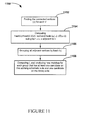
- FIG. 11 is a flow chart of a process for comparing schematic diagrams, in accordance with one embodiment of the invention.
- the invention provides a new method of deriving a schematic diagram, particularly as it relates to generating such diagrams in the reverse engineering of an integrated circuit (IC).
- the methods described herein enable the provision of a quality diagram, in some embodiments, comparable to what a person of ordinary skill in the art would appreciate consists of a good “textbook style” schematic diagram.
- the method will have as input, circuit information, including a plurality of circuit elements, provided for example, from a read back process performed on an IC.
- a first step in a reverse engineering process is schematically illustrated.
- a read back process 103 or other such process readily known in the art, is performed to extract the circuits and circuit elements present in the IC 102 .
- the read back process 103 may comprise an automated process, for example, as described in applicant's U.S. Pat. Nos. 6,907,583, 6,738,957 and 6,289,116, and co-pending United States Patent application No. 2006/0045325, all of which are herein incorporated by reference.
- the circuit elements extracted during the read back process 103 are generally provided as a so-called sea of gates 104 , an exemplary depiction of which is provided in FIG. 1B .
- the sea of gates 104 will contain basic circuit elements that might include, for example, single transistors, resistors, interconnects and single and/or isolated logic gates, to name a few.
- the circuit elements of the sea of gates 104 will generally be labelled with respect to the connections and/or signals thereto, the physical dimensions of the element and the pin co-ordinates, for example. It is noted that the electrical connections of the gates may generally be known, and implied through the same signal labelling at the pins, even though the connections between gates are not drawn in the exemplary sea of gates 104 of FIG. 1B .
- FIG. 2 a high level block diagram of a method of deriving a schematic diagram is presented.
- the working schematic diagram 202 is, at first, a sea of gates, such as the sea of gates 104 of FIG. 1B . While the working schematic diagram 202 is referred to as a schematic diagram for discussion purposes, it will be apparent to the skilled artisan that it does not present the circuit elements and their connectivity in a form that is traditionally found in a schematic diagram.
- a library 204 contains at least one collection of existing schematic diagrams, where each collection will include at least one good quality existing schematic diagram 206 therein, that is, at least one schematic diagram 206 whose quality is sufficient to satisfy the quality standards required for the application at hand.
- the library 204 will generally contain existing schematic diagrams from previous projects or libraries, including but not limited to, libraries of standard cells.
- the library 204 may contain schematic diagrams from different sources of good quality schematic diagrams.
- the IC such as IC 102 of FIG. 1A
- the IC may be a DRAM from a particular manufacturer. Schematics of a similar part from the same manufacturer might be in existence and contained within a library. This library could then be selected by the analyst to be included in the library 204 .
- Further existing schematic libraries may be selected for inclusion in library 204 such that the library 204 contain schematics considered likely to be relevant to the a schematic diagram associated with the IC to be reverse engineered. Accordingly, use of these existing schematics can reduce the effort required to derive the schematic diagram of circuits of the IC in question.
- the good quality schematic generated may be considered to be complete in terms of items including, but not limited to, connections, signals and layout information, and whose quality approaches the quality of a manually drawn schematic diagram, for example.
- the library 204 is searched for the existing schematic diagram 206 that presents the same components and connections of at least a portion of the working schematic diagram 202 . If a match is found, the existing schematic diagram 206 , or a portion thereof, is used to replace the matched portion of the working schematic diagram such that a revised, and possibly improved, working schematic diagram is produced.
- the searching and replacing steps of the method may comprise an iterative process that is continued until as large as possible a match is established between the existing schematic diagrams of the library 204 and the working schematic diagram 202 .
- the working schematic diagram 202 is drawn in a manner similar to that of the schematic diagrams of the library 204 .
- it is determined, either automatically via one or more quality threshold measures or via operator previewing and approval, that the working schematic diagram 202 is a good quality schematic and it becomes the good quality schematic 208 .
- FIG. 3 presents a flow chart of method 300 of deriving a good quality schematic diagram according to an embodiment of the invention.
- a working schematic diagram is displayed, where the working schematic diagram contains a plurality of circuit elements and will generally result from a read back process, such a the process 103 of FIG. 1A .
- at least one existing schematic diagram from a library is compared to a portion of the working schematic diagram. If a match is not found at step 304 the method returns to step 304 , via step 305 , to compare another existing schematic diagram.
- step 305 determines that there is a match between the portion and one of the existing schematic diagrams
- the portion is removed from the working schematic diagram at step 306 .
- the matching existing schematic diagram portion is then inserted into the working schematic diagram at step 308 , producing a revised working schematic diagram.
- step 310 it is queried as to whether the revised working schematic diagram is a good, or at least improved, schematic diagram. If the revised working schematic diagram is not of sufficient quality, the method returns to step 304 and the library of schematics is further considered to find a matching existing good schematic diagram. Finally, if the revised schematic diagram is considered to be of sufficient quality at step 310 , it is output at step 312 .
- a central feature of the method 300 is the matching of a portion of the working schematic diagram with a schematic diagram from the library of schematic diagrams at step 304 . Further embodiments of the invention will consider the methods implemented in step 304 in more detail.
- a basic premise of various embodiments is that portions of a working schematic diagram can be compared with and replaced by at least one existing schematic diagram in an automated manner, allowing for development of a good quality schematic diagram.
- FIG. 4A presents a working schematic diagram that is poorly organized and is not in a traditional format, as will be apparent to the skilled artisan.
- FIG. 4B presents a schematic diagram that is located within a selected library. While they appear quite different, the respective schematic diagrams of FIGS. 4A and 4A are in fact the same.
- the method of comparing, as presented in method 500 implements a starting point. Namely, so-called pivotal elements are identified, where an analyst considers the pivotal elements are likely part of a higher-level structure within the working schematic diagram and might be found in an existing schematic diagram. Therefore method 500 begins with receiving a selection of pivotal elements at step 502 .
- the elements E 3 404 and E 5 406 have been identified as pivotal elements.
- the selected pivotal elements are, in this case, unconnected which can lead to difficulties in subsequent calculations.
- a connected sub-graph is used.
- a connected pivotal graph 408 containing the pivotal elements E 3 404 and ES 406 is automatically produced at step 504 .
- the pivotal graph 408 contains connected elements E 3 , E 4 , E 5 , where element E 3 404 provides for connection of the selected pivotal elements.
- the algorithm for deriving such a connected sub-graph is, in the current embodiment, based on a breadth first search (BFS) algorithm.
- BFS breadth first search
- a selection of at least one target library of existing schematic diagrams is received.
- an analyst selects the target libraries.
- the selected target library will generally contain at least one existing schematic diagram, such as that presented in FIG. 4B .
- the target library may be pre-programmed. The automated selection of target libraries would consider various aspects of the IC being analyzed, including, but not limited to, the manufacturer, functionality and functional blocks thereof, for example.
- a pivotal graph is not implemented.
- a selection for at least a portion of the working schematic diagram is received.
- step 508 of FIG. 5A or step 524 of FIG. 5B at least a portion of the working schematic diagram is compared to at least one existing schematic diagram, or portion thereof, to determine if the at least one portion can be located within the existing schematic diagram. Additionally, at step 510 , any match that is located is expanded to incorporate a larger portion of the schematic diagram. In one embodiment, both of these processes implement techniques associated with sub-graph isomorphism.
- the first step in using sub-graph isomorphism is the conversion of the schematics to graphs that can be compared.
- the graph 602 comprises vertices such as vertex 604 and edges such as edge 606 .
- a schematic diagram might be considered as a graph G.
- a portion of the schematic is considered, which may in fact consist of individual gates. Such a portion may be considered a sub-graph of the graph G. Therefore, if G can be described by (V, E, Lv, Le), then S, which is a subset of V, defines a sub-graph thereof. Accordingly, the graph (S, ES, Lv, Le) can be called a sub-graph of G induced by S, where ES is a subset of edges that have both vertices within S.
- FIGS. 7A and 7B An example of the generation of a sub-graph from a schematic diagram is presented in FIGS. 7A and 7B .
- the schematic diagram of FIG. 7A contains an inverter 702 , a NOR gate 704 and a NAND gate 706 .
- the corresponding sub-graph is presented in FIG. 7B .
- a graph for a particular schematic diagram is developed assuming there is one vertex for each gate and if there is a connection between two gates, there are edges, going in both directions, between the connected gates. Therefore the graph of FIG. 7B contains a vertex for each gate of FIG. 7A and two (2) edges, one in each direction, for every connection between gates.
- the connection 703 produces the edges (OUT,A) and (A, OUT)
- the connection 705 produces the edges (A,A), (OUT,A) and (A,A), (A, OUT).
- the vertex labels Lv are the identifier of a group of equivalency of gates that can be substituted for each other for drawing purposes (e.g. the gates have similar functionality, size, and pin location, and can thus be depicted equivalently or similarly on a schematic diagram).
- a NOT gate can be deemed to be equivalent with a buffer and a diode, thereby providing the group id NOT;
- a NOR gate can be deemed equivalent with a NAND gate, thereby resulting in group id 2I.
- NOR gate 704 and NAND gate 706 can be considered replaceable for schematics drawing purposes—i.e. each schematics that looks good with NAND gate 706 will look good with NOR gate 704 .
- Le(v,u) may be defined as the list of the pairs (pinU, pinV), where pinU is the name of the pin associated with gate u, and pinV is the name of the pin associated with gate V.
- the list is sorted in lexicographical order.
- all instances of the pivotal graph 408 within the library of graphs are located using subgraph isomorphisms. More formally, the problem finds, for a given pivotal graph, all subsets of vertices of the graph(s) within the library where the induced subgraph is isomorphic with the pivotal graph. This is generally referred to as a NP complete program.
- Such programs are generally known by the skilled artisan and a substantial body of work surrounds the algorithms that address such programs from a practical view point. A good overview of such programs is provided in the paper by P. Foggia, C. Sansonne and M. Vento, “A performance comparison of five algorithms for graph isomorphism”, Workshop on Graph-based Representations in Pattern Recognition, May 23-25, 2001, the entire contents of which are incorporated herein by reference.
- FIG. 8 presents a method 800 , in accordance with one embodiment of the invention, for determining an invariant hash label for a given graph. It has been found that method 800 provides good practical performance for the graphs that result form schematic diagrams as would be found in a reverse engineering environment.
- a label ⁇ i representing the direct neighbourhood of a given vertex is calculated for each vertex.
- the label ⁇ i just calculated for a given vertex is integrated into the current label ⁇ i for this vertex. This calculation continues such that the vertices of the graph are becoming more distinguishable.
- a hash function for each ⁇ i (v) is calculated.
- a graphLabel is calculated for a given graph. For practical purposes, it is considered that graphs whose graphLabel computed at step 810 are equivalent are isomorphic. Theoretically this assumption may result in some false positives, but no false negatives. It has been found that this assumption has not led to any significant practical problems.
- the function sort used at steps 808 and 810 is a lexicographic sort of it's argument vector, which will be apparent to the skilled artisan.
- the method 800 implements a 64 bit hash function instead of using strings for graphLabels.
- a perfect hash function e.g. as described in Thomas H. Cormen, Charles E. Leiserson, Ronald L. Rivest, and Clifford Stein, Introduction to Algorithms, Second Edition, MIT Press and McGraw-Hill, 2001, Section 11.5: Perfect hashing, pp. 245-249
- an ordinary hash function e.g. CRC32
- CRC32 e.g. CRC32
- method 800 in the locating of matching sub-graphs and the expansion of the subsequent matches will now be considered with reference to FIGS. 9A to 9C , and in accordance with one embodiment of the invention.
- FIG. 9A presents two gates that are part of a working schematic diagram.
- the gates 902 , 904 and 906 all have known identities and connections.
- gate 902 is labelled as E 1 and has signals A 1 , A 2 and A 3 associated therewith;
- gate 904 is labelled as E 2 and has signals A 3 and A 4 associated therewith, and
- gate 906 is labelled as E 3 and has signals A 4 and A 5 associated therewith.
- the connectivity information i.e. signals, may be presented in a variety of formats.
- E 1 , E 2 and E 3 have string labels associated with their desired connections. This approach is outlined in applicant's United States Patent Application, published as 20070256037, the entire contents of which are incorporated herein by reference.
- FIG. 9B presents an existing schematic diagram 908 that is located within a library of existing schematics, and which comprises a diagram portion 910 comprising elements T 1 and T 2 similar to gates E 1 902 and E 2 904 of the pivotal graph.
- the gates 902 and 904 that form the pivotal graph, as well as the portion 910 of existing schematics 908 of the library, are therefore converted to sub-graphs and graphs, respectively, according to the techniques discussed above. It will generally be the case that there will be more than one existing schematic diagram in the library.
- the match may be expanded by determining if additional circuit elements of the working schematic diagram (e.g. element E 3 906 of FIG. 9A ) can be appended to the pivotal graph, and if the enlarged portion of the working schematic diagram can be located in at least one of the existing schematic diagrams.
- additional circuit elements of the working schematic diagram e.g. element E 3 906 of FIG. 9A
- element E 3 906 can be appended to the pivotal graph to form an enlarged portion, as a similar enlarged portion (e.g. schematic 910 ) is available in the library.
- This process thus leads to a revised or expanded schematic diagram 912 , as see in FIG. 9C .
- a flow chart depicting a process 1020 for expanding matching sub-graphs is depicted.
- all matching sub-graphs are put in a queue in step 1022 for use in generating a schematic diagram (e.g. as produced at step 504 of FIG. 5A ). While the queue is inactive and available, the most prospective match in the queue is selected at step 1024 and expanded at step 1026 , as described above.
- the recently expanded match is then returned to the cue at step 1028 .
- larger matches may thus be made available for selection from the queue as needed at step 1030 .
- a process 1150 is presented for implementing a match expanding step, such as step 1026 of FIG. 10 .
- the selected match is expanded by first identifying the connected vertices thereof in step 1152 , and implementing a series of computations as identified by steps 1154 , 1156 and 1158 , and described above, for producing new matches to be added to the queue for use in generating the schematic diagram.
Landscapes
- Engineering & Computer Science (AREA)
- Computer Hardware Design (AREA)
- Physics & Mathematics (AREA)
- Theoretical Computer Science (AREA)
- Evolutionary Computation (AREA)
- Geometry (AREA)
- General Engineering & Computer Science (AREA)
- General Physics & Mathematics (AREA)
- Design And Manufacture Of Integrated Circuits (AREA)
Abstract
Description
G=(V,E,Lv,Le)
where V is a finite set of vertices; E is a set of the edges and subset of V2; Lv are labels associated with the vertices, such that Lv: V-> strings; and Le is the set of labels assigned to edges, such that Le: E-> strings.
V={1,2,3,4};
E={(4,3),(3,4),(3,1),(1,2)};
Lv(1)=B,Lv(2)=A,Lv(3)=C,Lv(4)=D; and
Le(3,4)=W,Le(4,3)=Z,Le(3,1)=Y,Le(1,2)=X.
Lv1(v)=Lv2(I(v)),Le1(u,v)=Le2((I(u),I(v)).
Claims (13)
Applications Claiming Priority (1)
| Application Number | Priority Date | Filing Date | Title |
|---|---|---|---|
| PCT/CA2008/000734 WO2009127035A1 (en) | 2008-04-18 | 2008-04-18 | Method of deriving an integrated circuit schematic diagram |
Publications (2)
| Publication Number | Publication Date |
|---|---|
| US20110041110A1 US20110041110A1 (en) | 2011-02-17 |
| US8347262B2 true US8347262B2 (en) | 2013-01-01 |
Family
ID=41198719
Family Applications (1)
| Application Number | Title | Priority Date | Filing Date |
|---|---|---|---|
| US12/989,739 Active 2028-08-24 US8347262B2 (en) | 2008-04-18 | 2008-04-18 | Method of deriving an integrated circuit schematic diagram |
Country Status (4)
| Country | Link |
|---|---|
| US (1) | US8347262B2 (en) |
| CN (1) | CN101663665B (en) |
| CA (1) | CA2719835C (en) |
| WO (1) | WO2009127035A1 (en) |
Cited By (2)
| Publication number | Priority date | Publication date | Assignee | Title |
|---|---|---|---|---|
| US10354037B1 (en) * | 2016-06-30 | 2019-07-16 | Cadence Design Systems, Inc. | Methods, systems, and computer program product for implementing an electronic design by manipulating a hierarchical structure of the electronic design |
| US11080443B2 (en) * | 2017-12-20 | 2021-08-03 | International Business Machines Corporation | Memory element graph-based placement in integrated circuit design |
Families Citing this family (5)
| Publication number | Priority date | Publication date | Assignee | Title |
|---|---|---|---|---|
| US8108823B2 (en) * | 2008-06-18 | 2012-01-31 | International Business Machines Corporation | User selected grid for logically representing an electronic circuit |
| CN102486807A (en) * | 2010-12-03 | 2012-06-06 | 北京晶智意达科技有限公司 | Sub circuit signature method on basis of subgraph isomorphism |
| US8464191B2 (en) * | 2011-07-21 | 2013-06-11 | R3 Logic, Inc. | System and method for identifying circuit components of an integrated circuit |
| CN103324768A (en) * | 2012-03-21 | 2013-09-25 | 苏州芯禾电子科技有限公司 | Quickly marking method of schematic circuit diagram |
| US8984459B2 (en) * | 2012-05-04 | 2015-03-17 | Taiwan Semiconductor Manufacturing Company, Ltd. | Methods and apparatus for layout verification |
Citations (8)
| Publication number | Priority date | Publication date | Assignee | Title |
|---|---|---|---|---|
| US5287511A (en) * | 1988-07-11 | 1994-02-15 | Star Semiconductor Corporation | Architectures and methods for dividing processing tasks into tasks for a programmable real time signal processor and tasks for a decision making microprocessor interfacing therewith |
| US5448493A (en) * | 1989-12-20 | 1995-09-05 | Xilinx, Inc. | Structure and method for manually controlling automatic configuration in an integrated circuit logic block array |
| US5555270A (en) * | 1995-03-13 | 1996-09-10 | Motorola Inc. | Method and apparatus for constructing unique input/output sequence (UIO) sets utilizing transition distinctness measurements |
| US5598344A (en) * | 1990-04-06 | 1997-01-28 | Lsi Logic Corporation | Method and system for creating, validating, and scaling structural description of electronic device |
| US6438734B1 (en) * | 1997-10-06 | 2002-08-20 | Agilent Technologies, Inc. | Fast search method for enabling a computer to find elementary loops in a graph |
| US6536018B1 (en) | 2000-06-05 | 2003-03-18 | The University Of Chicago | Reverse engineering of integrated circuits |
| US7073141B2 (en) | 2003-11-25 | 2006-07-04 | Intel Corporation | Device, system and method for VLSI design analysis |
| US20080250213A1 (en) * | 2007-04-06 | 2008-10-09 | Holt John M | Computer Architecture And Method Of Operation for Multi-Computer Distributed Processing Having Redundant Array Of Independent Systems With Replicated Memory And Code Striping |
Family Cites Families (1)
| Publication number | Priority date | Publication date | Assignee | Title |
|---|---|---|---|---|
| CN1523660A (en) * | 2003-02-17 | 2004-08-25 | 上海芯华微电子有限公司 | Bidirectional Technology System for Integrated Circuit Design |
-
2008
- 2008-04-18 US US12/989,739 patent/US8347262B2/en active Active
- 2008-04-18 WO PCT/CA2008/000734 patent/WO2009127035A1/en not_active Ceased
- 2008-04-18 CN CN200880000047.0A patent/CN101663665B/en active Active
- 2008-04-18 CA CA2719835A patent/CA2719835C/en active Active
Patent Citations (10)
| Publication number | Priority date | Publication date | Assignee | Title |
|---|---|---|---|---|
| US5287511A (en) * | 1988-07-11 | 1994-02-15 | Star Semiconductor Corporation | Architectures and methods for dividing processing tasks into tasks for a programmable real time signal processor and tasks for a decision making microprocessor interfacing therewith |
| US5524244A (en) * | 1988-07-11 | 1996-06-04 | Logic Devices, Inc. | System for dividing processing tasks into signal processor and decision-making microprocessor interfacing therewith |
| US5448493A (en) * | 1989-12-20 | 1995-09-05 | Xilinx, Inc. | Structure and method for manually controlling automatic configuration in an integrated circuit logic block array |
| US5598344A (en) * | 1990-04-06 | 1997-01-28 | Lsi Logic Corporation | Method and system for creating, validating, and scaling structural description of electronic device |
| US6216252B1 (en) * | 1990-04-06 | 2001-04-10 | Lsi Logic Corporation | Method and system for creating, validating, and scaling structural description of electronic device |
| US5555270A (en) * | 1995-03-13 | 1996-09-10 | Motorola Inc. | Method and apparatus for constructing unique input/output sequence (UIO) sets utilizing transition distinctness measurements |
| US6438734B1 (en) * | 1997-10-06 | 2002-08-20 | Agilent Technologies, Inc. | Fast search method for enabling a computer to find elementary loops in a graph |
| US6536018B1 (en) | 2000-06-05 | 2003-03-18 | The University Of Chicago | Reverse engineering of integrated circuits |
| US7073141B2 (en) | 2003-11-25 | 2006-07-04 | Intel Corporation | Device, system and method for VLSI design analysis |
| US20080250213A1 (en) * | 2007-04-06 | 2008-10-09 | Holt John M | Computer Architecture And Method Of Operation for Multi-Computer Distributed Processing Having Redundant Array Of Independent Systems With Replicated Memory And Code Striping |
Cited By (2)
| Publication number | Priority date | Publication date | Assignee | Title |
|---|---|---|---|---|
| US10354037B1 (en) * | 2016-06-30 | 2019-07-16 | Cadence Design Systems, Inc. | Methods, systems, and computer program product for implementing an electronic design by manipulating a hierarchical structure of the electronic design |
| US11080443B2 (en) * | 2017-12-20 | 2021-08-03 | International Business Machines Corporation | Memory element graph-based placement in integrated circuit design |
Also Published As
| Publication number | Publication date |
|---|---|
| CN101663665B (en) | 2014-07-09 |
| US20110041110A1 (en) | 2011-02-17 |
| CA2719835C (en) | 2014-07-15 |
| CN101663665A (en) | 2010-03-03 |
| WO2009127035A1 (en) | 2009-10-22 |
| CA2719835A1 (en) | 2009-10-22 |
Similar Documents
| Publication | Publication Date | Title |
|---|---|---|
| US8347262B2 (en) | Method of deriving an integrated circuit schematic diagram | |
| US8701058B2 (en) | Integrated circuit analysis systems and methods | |
| US7480878B2 (en) | Method and system for layout versus schematic validation of integrated circuit designs | |
| US8069426B2 (en) | Method and mechanism for identifying and tracking shape connectivity | |
| US7908579B2 (en) | Method and mechanism for extraction and recognition of polygons in an IC design | |
| CN105095607A (en) | Optimization method for netlist logic redundancies in ASIC design and optimization system for netlist logic redundancy in ASIC design | |
| CN112836735A (en) | An Optimized Random Forest Approach to Handling Imbalanced Datasets | |
| CN118228645A (en) | Integrated circuit analysis method, system and device based on subgraph matching | |
| Ferreira et al. | Automatically generating websites from hand-drawn mockups | |
| CN104933442A (en) | Method for propagating image label based on minimal cost path | |
| US7421671B2 (en) | Graph pruning scheme for sensitivity analysis with partitions | |
| US20120290282A1 (en) | Reachability analysis by logical circuit simulation for providing output sets containing symbolic values | |
| CN106202007B (en) | A Method for Evaluating the Similarity of MATLAB Program Files | |
| Rosiello et al. | A hash-based approach for functional regularity extraction during logic synthesis | |
| CN110955892A (en) | A hardware Trojan detection method based on machine learning and circuit behavior-level features | |
| CN113051858A (en) | Method for detecting suspicious circuit of FPGA (field programmable Gate array) software based on subgraph isomorphism | |
| US9697315B2 (en) | System and method for displaying a device using an automated tool | |
| US6754878B1 (en) | Recognizing structure information from a netlist | |
| US8607175B1 (en) | Identifying logic blocks in a synthesized logic design that have specified inputs | |
| AU2017225022A1 (en) | Method, system and apparatus for processing image data | |
| JP2005038357A (en) | Logical equivalence verification device, logical equivalence verification method, control program, and readable recording medium | |
| US9087175B2 (en) | Information processing apparatus and design verification method | |
| Lee et al. | SOFA-H: Post-Synthesis Area Optimization via Functionally Encoded, Net-Driven Subgraph Mining and SAT-Based Hypercell Remapping | |
| WO2025147772A1 (en) | Computer-implemented methods for compressing a digital connectivity representation of an integrated circuit | |
| CN121884385A (en) | CAD drawing equipment type identification method and system based on embedded model |
Legal Events
| Date | Code | Title | Description |
|---|---|---|---|
| AS | Assignment |
Owner name: SEMICONDUCTOR INSIGHTS INC., CANADA Free format text: ASSIGNMENT OF ASSIGNORS INTEREST;ASSIGNORS:ZAVADSKY, VYACHESLAV;KEYES, EDWARD;EDMONDS, SHANE;AND OTHERS;SIGNING DATES FROM 20110103 TO 20110118;REEL/FRAME:027196/0199 |
|
| FEPP | Fee payment procedure |
Free format text: PAYOR NUMBER ASSIGNED (ORIGINAL EVENT CODE: ASPN); ENTITY STATUS OF PATENT OWNER: LARGE ENTITY |
|
| STCF | Information on status: patent grant |
Free format text: PATENTED CASE |
|
| AS | Assignment |
Owner name: TECHINSIGHTS INC., CANADA Free format text: CHANGE OF NAME;ASSIGNOR:SEMICONDUCTOR INSIGHTS INC.;REEL/FRAME:033941/0692 Effective date: 20140821 |
|
| FPAY | Fee payment |
Year of fee payment: 4 |
|
| AS | Assignment |
Owner name: STELLUS CAPITAL INVESTMENT CORPORATION, AS ADMINISTRATIVE AGENT, TEXAS Free format text: NOTICE OF GRANT OF SECURITY INTEREST IN PATENTS;ASSIGNOR:TECHINSIGHTS INC.;REEL/FRAME:043571/0385 Effective date: 20170816 Owner name: STELLUS CAPITAL INVESTMENT CORPORATION, AS ADMINIS Free format text: NOTICE OF GRANT OF SECURITY INTEREST IN PATENTS;ASSIGNOR:TECHINSIGHTS INC.;REEL/FRAME:043571/0385 Effective date: 20170816 |
|
| MAFP | Maintenance fee payment |
Free format text: PAYMENT OF MAINTENANCE FEE, 8TH YEAR, LARGE ENTITY (ORIGINAL EVENT CODE: M1552); ENTITY STATUS OF PATENT OWNER: LARGE ENTITY Year of fee payment: 8 |
|
| AS | Assignment |
Owner name: CAPITAL ONE, NATIONAL ASSOCIATION, DELAWARE Free format text: SECURITY INTEREST;ASSIGNORS:TECHINSIGHTS INC.;VLSI RESEARCH INC.;REEL/FRAME:058096/0721 Effective date: 20211109 |
|
| AS | Assignment |
Owner name: TECHINSIGHTS INC., CANADA Free format text: RELEASE BY SECURED PARTY;ASSIGNOR:STELLUS CAPITAL INVESTMENT CORPORATION, AS ADMINISTRATIVE AGENT;REEL/FRAME:058096/0558 Effective date: 20211109 |