US8338280B2 - Method for fabricating nano devices - Google Patents
Method for fabricating nano devices Download PDFInfo
- Publication number
- US8338280B2 US8338280B2 US12/832,082 US83208210A US8338280B2 US 8338280 B2 US8338280 B2 US 8338280B2 US 83208210 A US83208210 A US 83208210A US 8338280 B2 US8338280 B2 US 8338280B2
- Authority
- US
- United States
- Prior art keywords
- nano
- substrate
- crystalline layer
- wires
- layer
- Prior art date
- Legal status (The legal status is an assumption and is not a legal conclusion. Google has not performed a legal analysis and makes no representation as to the accuracy of the status listed.)
- Active, expires
Links
- 238000000034 method Methods 0.000 title claims abstract description 82
- 239000002070 nanowire Substances 0.000 claims abstract description 117
- 230000007547 defect Effects 0.000 claims abstract description 76
- 239000002159 nanocrystal Substances 0.000 claims abstract description 62
- 239000000758 substrate Substances 0.000 claims abstract description 52
- 239000007943 implant Substances 0.000 claims description 20
- 230000001590 oxidative effect Effects 0.000 claims description 18
- 238000000137 annealing Methods 0.000 claims description 16
- 150000002500 ions Chemical class 0.000 claims description 11
- 239000006117 anti-reflective coating Substances 0.000 claims description 8
- 239000004065 semiconductor Substances 0.000 claims description 7
- 238000005280 amorphization Methods 0.000 claims description 5
- 238000005530 etching Methods 0.000 claims description 5
- 238000004090 dissolution Methods 0.000 claims description 3
- 229910021417 amorphous silicon Inorganic materials 0.000 claims 8
- 238000000151 deposition Methods 0.000 claims 2
- 230000003647 oxidation Effects 0.000 claims 2
- 238000007254 oxidation reaction Methods 0.000 claims 2
- 238000004519 manufacturing process Methods 0.000 abstract description 6
- 239000010410 layer Substances 0.000 description 53
- 230000008569 process Effects 0.000 description 48
- 239000000463 material Substances 0.000 description 11
- VYPSYNLAJGMNEJ-UHFFFAOYSA-N Silicium dioxide Chemical compound O=[Si]=O VYPSYNLAJGMNEJ-UHFFFAOYSA-N 0.000 description 9
- XUIMIQQOPSSXEZ-UHFFFAOYSA-N Silicon Chemical compound [Si] XUIMIQQOPSSXEZ-UHFFFAOYSA-N 0.000 description 9
- 229910052710 silicon Inorganic materials 0.000 description 9
- 239000010703 silicon Substances 0.000 description 9
- 239000002178 crystalline material Substances 0.000 description 8
- 238000001020 plasma etching Methods 0.000 description 8
- 239000002019 doping agent Substances 0.000 description 7
- 238000005229 chemical vapour deposition Methods 0.000 description 5
- 239000011159 matrix material Substances 0.000 description 5
- 230000015572 biosynthetic process Effects 0.000 description 4
- 229910052681 coesite Inorganic materials 0.000 description 4
- 229910052906 cristobalite Inorganic materials 0.000 description 4
- 239000002096 quantum dot Substances 0.000 description 4
- 239000000377 silicon dioxide Substances 0.000 description 4
- 229910052682 stishovite Inorganic materials 0.000 description 4
- 229910052905 tridymite Inorganic materials 0.000 description 4
- 238000009826 distribution Methods 0.000 description 3
- 230000000694 effects Effects 0.000 description 3
- 238000000059 patterning Methods 0.000 description 3
- 238000004151 rapid thermal annealing Methods 0.000 description 3
- 230000005641 tunneling Effects 0.000 description 3
- 229910000577 Silicon-germanium Inorganic materials 0.000 description 2
- LEVVHYCKPQWKOP-UHFFFAOYSA-N [Si].[Ge] Chemical compound [Si].[Ge] LEVVHYCKPQWKOP-UHFFFAOYSA-N 0.000 description 2
- 239000013078 crystal Substances 0.000 description 2
- 238000005516 engineering process Methods 0.000 description 2
- 230000006870 function Effects 0.000 description 2
- 238000002513 implantation Methods 0.000 description 2
- 239000012212 insulator Substances 0.000 description 2
- 238000001459 lithography Methods 0.000 description 2
- 230000007246 mechanism Effects 0.000 description 2
- 239000002086 nanomaterial Substances 0.000 description 2
- 229920002120 photoresistant polymer Polymers 0.000 description 2
- 229910021420 polycrystalline silicon Inorganic materials 0.000 description 2
- -1 silicon ions Chemical class 0.000 description 2
- ZOXJGFHDIHLPTG-UHFFFAOYSA-N Boron Chemical compound [B] ZOXJGFHDIHLPTG-UHFFFAOYSA-N 0.000 description 1
- OAICVXFJPJFONN-UHFFFAOYSA-N Phosphorus Chemical compound [P] OAICVXFJPJFONN-UHFFFAOYSA-N 0.000 description 1
- 229910052581 Si3N4 Inorganic materials 0.000 description 1
- 229910052785 arsenic Inorganic materials 0.000 description 1
- RQNWIZPPADIBDY-UHFFFAOYSA-N arsenic atom Chemical compound [As] RQNWIZPPADIBDY-UHFFFAOYSA-N 0.000 description 1
- 229910052796 boron Inorganic materials 0.000 description 1
- 230000008859 change Effects 0.000 description 1
- 230000000295 complement effect Effects 0.000 description 1
- 229910021419 crystalline silicon Inorganic materials 0.000 description 1
- 238000001941 electron spectroscopy Methods 0.000 description 1
- 238000002474 experimental method Methods 0.000 description 1
- 229910052732 germanium Inorganic materials 0.000 description 1
- GNPVGFCGXDBREM-UHFFFAOYSA-N germanium atom Chemical compound [Ge] GNPVGFCGXDBREM-UHFFFAOYSA-N 0.000 description 1
- 230000010354 integration Effects 0.000 description 1
- 238000005468 ion implantation Methods 0.000 description 1
- 238000005224 laser annealing Methods 0.000 description 1
- 229910052751 metal Inorganic materials 0.000 description 1
- 239000002184 metal Substances 0.000 description 1
- 229910044991 metal oxide Inorganic materials 0.000 description 1
- 150000004706 metal oxides Chemical class 0.000 description 1
- 238000004377 microelectronic Methods 0.000 description 1
- 229910052698 phosphorus Inorganic materials 0.000 description 1
- 239000011574 phosphorus Substances 0.000 description 1
- 229920005591 polysilicon Polymers 0.000 description 1
- HQVNEWCFYHHQES-UHFFFAOYSA-N silicon nitride Chemical compound N12[Si]34N5[Si]62N3[Si]51N64 HQVNEWCFYHHQES-UHFFFAOYSA-N 0.000 description 1
- 229910052814 silicon oxide Inorganic materials 0.000 description 1
- 230000001629 suppression Effects 0.000 description 1
- 239000002344 surface layer Substances 0.000 description 1
- 230000032258 transport Effects 0.000 description 1
Images


Classifications
-
- H—ELECTRICITY
- H01—ELECTRIC ELEMENTS
- H01L—SEMICONDUCTOR DEVICES NOT COVERED BY CLASS H10
- H01L29/00—Semiconductor devices adapted for rectifying, amplifying, oscillating or switching, or capacitors or resistors with at least one potential-jump barrier or surface barrier, e.g. PN junction depletion layer or carrier concentration layer; Details of semiconductor bodies or of electrodes thereof ; Multistep manufacturing processes therefor
- H01L29/66—Types of semiconductor device ; Multistep manufacturing processes therefor
- H01L29/66007—Multistep manufacturing processes
- H01L29/66075—Multistep manufacturing processes of devices having semiconductor bodies comprising group 14 or group 13/15 materials
- H01L29/66227—Multistep manufacturing processes of devices having semiconductor bodies comprising group 14 or group 13/15 materials the devices being controllable only by the electric current supplied or the electric potential applied, to an electrode which does not carry the current to be rectified, amplified or switched, e.g. three-terminal devices
- H01L29/66409—Unipolar field-effect transistors
- H01L29/66439—Unipolar field-effect transistors with a one- or zero-dimensional channel, e.g. quantum wire FET, in-plane gate transistor [IPG], single electron transistor [SET], striped channel transistor, Coulomb blockade transistor
-
- B—PERFORMING OPERATIONS; TRANSPORTING
- B82—NANOTECHNOLOGY
- B82Y—SPECIFIC USES OR APPLICATIONS OF NANOSTRUCTURES; MEASUREMENT OR ANALYSIS OF NANOSTRUCTURES; MANUFACTURE OR TREATMENT OF NANOSTRUCTURES
- B82Y10/00—Nanotechnology for information processing, storage or transmission, e.g. quantum computing or single electron logic
-
- H—ELECTRICITY
- H01—ELECTRIC ELEMENTS
- H01L—SEMICONDUCTOR DEVICES NOT COVERED BY CLASS H10
- H01L29/00—Semiconductor devices adapted for rectifying, amplifying, oscillating or switching, or capacitors or resistors with at least one potential-jump barrier or surface barrier, e.g. PN junction depletion layer or carrier concentration layer; Details of semiconductor bodies or of electrodes thereof ; Multistep manufacturing processes therefor
- H01L29/02—Semiconductor bodies ; Multistep manufacturing processes therefor
- H01L29/06—Semiconductor bodies ; Multistep manufacturing processes therefor characterised by their shape; characterised by the shapes, relative sizes, or dispositions of the semiconductor regions ; characterised by the concentration or distribution of impurities within semiconductor regions
- H01L29/0657—Semiconductor bodies ; Multistep manufacturing processes therefor characterised by their shape; characterised by the shapes, relative sizes, or dispositions of the semiconductor regions ; characterised by the concentration or distribution of impurities within semiconductor regions characterised by the shape of the body
- H01L29/0665—Semiconductor bodies ; Multistep manufacturing processes therefor characterised by their shape; characterised by the shapes, relative sizes, or dispositions of the semiconductor regions ; characterised by the concentration or distribution of impurities within semiconductor regions characterised by the shape of the body the shape of the body defining a nanostructure
-
- H—ELECTRICITY
- H01—ELECTRIC ELEMENTS
- H01L—SEMICONDUCTOR DEVICES NOT COVERED BY CLASS H10
- H01L29/00—Semiconductor devices adapted for rectifying, amplifying, oscillating or switching, or capacitors or resistors with at least one potential-jump barrier or surface barrier, e.g. PN junction depletion layer or carrier concentration layer; Details of semiconductor bodies or of electrodes thereof ; Multistep manufacturing processes therefor
- H01L29/66—Types of semiconductor device ; Multistep manufacturing processes therefor
- H01L29/68—Types of semiconductor device ; Multistep manufacturing processes therefor controllable by only the electric current supplied, or only the electric potential applied, to an electrode which does not carry the current to be rectified, amplified or switched
- H01L29/76—Unipolar devices, e.g. field effect transistors
- H01L29/7613—Single electron transistors; Coulomb blockade devices
Definitions
- CMOS complementary metal-oxide semiconductor
- the single electron tunneling transistor is one of the potential novel devices which have recently received much attention due to their small size, unique device functionality and low power consumption.
- the SET typically transports charges across the source to the drain via nano-size single quantum dot (QD).
- QD nano-size single quantum dot
- the operation mechanism is based on the Coulomb blockade effect on a nano-scale conduction island which causes strong suppression of the tunneling charge until the island is discharged by exactly one charge.
- Embodiments relate to a method for fabricating nano-wires in nano-devices, and more particularly to nano-device fabrication using end-of-range (EOR) defects.
- EOR end-of-range
- the method comprises providing a substrate with a surface crystalline layer over the substrate, creating end-of-range (EOR) defects in the surface crystalline layer, forming one or more fins with EOR defects embedded within and oxidizing the one or more fins to form one or more fully oxidized nano-wires with nano-crystals within the core of the nano-wire.
- EOR end-of-range
- the method comprises providing a substrate with a surface crystalline layer over the substrate, creating end-of-range (EOR) defects in the surface crystalline layer, forming one or more fins with EOR defects embedded within, oxidizing the one or more fins, removing the oxide from the one or more fins to form one or more nano-wires and oxidizing the one or more nano-wires to form one or more fully oxidized nano-wires with nano-crystals within the core of the nano-wire.
- EOR end-of-range
- FIGS. 2 b - c show side and cross-sectional views of various embodiments of nano-wires
- FIGS. 2 d - f show alternative embodiments of nano-wire arrangements
- FIGS. 3 a - d show plan and side views of embodiments of devices incorporating nano-wires
- FIGS. 4 a - i show cross-sectional and plan views of a process for forming a device with a nano-wire
- FIGS. 5 a - b show cross-sectional and plan views of an alternative process for forming a device with a nano-wire
- FIGS. 6 a - c show cross-sectional and plan views of an alternative process for forming a device with nano-wires
- FIGS. 7 a - c show cross-sectional and plan views of an alternative process for forming a device with nano-wires.
- FIG. 8 shows cross-sectional and plan views of yet another process for forming a device with nano-wires.
- Embodiments relate to nano-wires and methods of fabricating nano-wires.
- the nano-wires can be employed in nano-devices or structures.
- the nano-wires are incorporated in a SET device.
- Such SET devices can be used to form ICs, such as voltage or charge state logics.
- the devices can be incorporated into consumer electronic products, such as single-electron spectroscopy, electrometers and memory, such as random access memory (RAM) devices.
- RAM random access memory
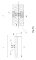
- FIG. 1 shows an embodiment of a nano-structure 100 .
- the nano-structure is formed on a substrate 101 .
- the substrate comprises a crystalline-on-insulator (COI) substrate.
- the substrate for example, comprises a top or surface silicon layer 107 and a bulk silicon 103 with a buried oxide (BOX) 105 therebetween to form a silicon-on-insulator (SOI) substrate.
- SOI silicon-on-insulator
- SOI silicon-on-insulator
- SOI silicon-on-insulator
- SOI silicon-on-insulator
- the surface layer can be patterned to form first and second contact regions 120 and 130 .
- the contact regions for example, comprise doped regions formed on the surface silicon layer.
- the doped regions can comprise first polarity type dopants.
- the first polarity type dopants for example, are p-type dopants. Alternatively, n-type dopants are used to form the doped regions. Providing other types of contact regions may also be useful.
- the contact regions for example, may serve as source and drain pads of a SET.
- the nano-wire comprises an oxide support structure 113 containing nano-crystals or nano-clusters 115 .
- the support structure of the nano-wire may have a cross-sectional size of, for example, about 20-30 nm in diameters. Forming support structures having other sizes may also be useful.
- the nano-crystals are uniformly distributed within the support structure.
- the nano-crystals may also have a uniform size of about 5-10 nm in diameter. In some instances, the term nano-crystals and nano-clusters may be used interchangeably.
- the nano-crystals may comprise a semiconductor material.
- the nano-crystals comprise, for example, silicon. Providing nano-crystals of other types of semiconductor materials may also be useful.
- the nano-crystals are derived from end-of-range (EOR) defects created from a pre-amorphization implant (PAI) process.
- the PAI process implants ions into a crystalline substrate or layer.
- the PAI implants silicon ions (Si + ).
- Other types of ions, such as Ge + may also be useful.
- the PAI renders the crystalline material amorphous.
- EOR defects are located at the interface of the amorphous and crystalline materials. By selecting the appropriate implant energy, the EOR defect depth can be precisely controlled in the crystalline substrate or layer.
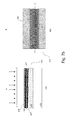
- FIG. 2 a shows experimental results correlating PAI energy of Si + ions and depth of EOR.
- the experiment was conducted by implanting Si + ions in an SOI substrate in which the surface crystalline layer is about 5000 ⁇ thick.
- the PAI dose is about 1 ⁇ 10 16 cm ⁇ 2 .
- depth of EOR defects increases with PAI energy. For example, the higher the PAI energy, the deeper the EOR defects are from the surface of the crystalline layer.
- the EOR defects can be precisely located in a crystalline material. This enables nano-crystals to be formed with uniform size and distribution within the nano-wire.
- the ability to uniformly distribute the nano-crystals with uniform size in the nano-wire ensures the proper function of the device as the spatial distance between nano-crystals should not be too far apart. In the event adjacent nano-crystals are too far apart, the device will fail to function as a charge cannot transmit through the insulating SiO 2 .
- the charge transfer mechanism is by quantum mechanical tunneling. For example, when two quantum dots (nano-crystals) are in close proximity, the charge can tunnel (or penetrate) through the oxide separating the two nano-crystals by the application of a voltage.
- the flow and direction of flow can be controlled by, for example, applying the appropriate bias voltage between the contact regions.
- nano-crystals are derived from EOR defects.
- EOR defects enables the nano-crystals to be precisely located at desired locations of a device.
- the nano-crystals are formed from multiple oxidizing annealing processes.
- the nano-crystals are formed using a single oxidizing annealing process.
- implant dosages and annealing conditions to form the nano-crystals in an oxide support structure are lower than those required to form conventional silicon nano-wires.
- FIGS. 2 b - c show side and cross-sectional views of various embodiments of nano-wires.
- a nano-wire 110 is shown.
- Nano-crystals 113 are distributed in a single row within the nano-wire.
- the row of nano-crystals may include a plurality of nano-crystals or nano-crystal clusters. Providing a row of single crystals or a combination of single nano-crystals and nano-crystal clusters may also be useful.
- nano-crystals 113 are distributed in multiple rows 112 1-n , wherein n is a whole number.
- the nano-crystals are, for example, distributed in 3 rows.
- the nano-crystals may also be distributed in other number of rows. The number of rows may depend on, for example, the size of the support structure and nano-crystals.
- the row of nano-crystals may include a plurality of nano-crystals or nano-crystal clusters. Providing a row of single crystals or a combination of single nano-crystals and nano-crystal clusters may also be useful.
- first and second nano-wires 110 1 and 110 2 can be arranged in a column in the y direction between first and second contact regions 120 and 130 , as shown in FIG. 2 d .
- the first and second nano-wires form, for example, a twin nano-wire arrangement. Providing more than two nano-wires in the column direction may also be useful.
- a plurality of nano-wires 110 1-m where m ⁇ 2, are arranged in a row in the x direction between first and second contact regions 120 and 130 , as shown in FIG. 2 e .
- multiple nano-wires may be provided in both column and row directions.
- the multiple nano-wires may be arranged as a 2 ⁇ 3 matrix of nano-wires. Arranging the multiple nano-wires in other size matrices may also be useful.
- the multiple nano-wires are arranged in a 2 ⁇ m matrix.
- a soft mask layer 480 is formed on the substrate surface.
- the soft mask comprises photoresist.
- the soft mask may be formed by spin on techniques.
- the soft mask is patterned to create an opening for selectively processing the substrate. Patterning the soft mask can be achieved by selectively exposing it to an exposure source with a photomask containing the desired pattern.
- the soft mask is developed after exposure, transferring the pattern of the photomask to the soft mask.
- an anti-reflective coating (ARC) layer may be provided below the soft mask.
- the ARC for example, may be an organic or inorganic ARC. Other types of ARC materials may also be useful.
- Various techniques, such as CVD or spin on, may be employed to form the ARC.
- the portion of the ARC exposed by the patterned soft mask may be removed by, for example, an anisotropic etch such as reactive ion etch (RIE).
- RIE reactive ion etch
- the substrate is processed to create end-of-range (EOR) defects 422 in the surface crystalline layer.
- EOR defects are created by a pre-amorphization implant (PAI).
- PAI pre-amorphization implant
- the PAI transforms an upper or surface portion 426 of the surface crystalline layer to an amorphous ( ⁇ ) layer.
- ⁇ amorphous
- the PAI transforms the surface crystalline Si layer to an ⁇ -Si layer.
- a lower portion 427 of the surface crystalline layer below the EOR defects remains crystalline in structure.
- the PAI may implant various types of ions into the substrate.
- the PAI may implant Si + or Ge + ions into the surface crystalline layer. Implanting other types of ions or a combination of different types of ions may also be useful.
- the parameters of the PAI may be tailored to produce EOR defects at the desired depth in the surface crystalline layer. In one embodiment, the location of the EOR defects corresponds to the location of the nano-crystals of the nano-wire to be formed.
- the dose of the implant should be sufficient to form nano-crystals with the desired distribution in the nano-wire.
- the implant dose corresponds to the EOR defect density.
- the dose should be sufficiently high to form high EOR defect density as a high EOR defect density may be desirable.
- some EOR defects may dissolve due to various thermal processes of the fabrication process. By having a high EOR defect density, this may ensure the formation of nano-crystals having the desired distribution in spite of loss of EOR defects during processing.
- the PAI dose is from 1 ⁇ 10 15 cm ⁇ 2 to 1 ⁇ 10 17 cm ⁇ 2 .
- the PAI energy determines the depth of EOR defects.
- the PAI dose and energy are selected to avoid fully amorphizing the crystalline layer.
- the PAI dose and energy are selected to avoid fully amorphizing the surface crystalline layer of the COI substrate.
- the soft mask 480 may be removed.
- the substrate is subjected to an anneal to recrystallize the ⁇ -Si layer to form a crystalline layer 428 .
- the anneal for example, comprises a rapid thermal annealing (RTA).
- RTA rapid thermal annealing
- Other annealing process for example, spike annealing, laser annealing or flash annealing may also be used.
- the anneal should have a sufficiently low thermal budget to reduce or avoid excessive dissolution of EOR defects.
- the anneal also stabilizes the defects which reduces their susceptibility to dissolution by further thermal processes.
- the anneal comprises a low temperature RTA. Performing an anneal while maintaining a sufficiently low thermal budget using other parameters may also be useful.
- the fin or post 450 is oxidized.
- the fin is oxidized after removal of the hard mask layer.
- Oxidizing the fin in one embodiment, forms a crystalline nano-wire core 452 .
- oxidizing the fin forms a silicon nano-wire core.
- the nano-wire core for example, comprises crystalline material 454 surrounding EOR defects 422 .
- Oxidizing the fin is achieved by subjecting the substrate to an anneal in an oxidizing ambient. In one embodiment, a furnace anneal is employed. Other types of anneals may also be useful. In one embodiment, the anneal is performed at a temperature of about 1100° C. for about 5 hours in an oxidizing ambient. Forming the nano-wire core may also form a thin oxide layer in other parts of the crystalline layer exposed by the removal of the mask, for example, the pad regions.
- the oxide is removed selective to the crystalline material.
- the oxide surrounding the nano-wire core and on the surface of the crystalline material of the substrate is removed.
- the oxide is removed by, for example, an etch.
- the etch in one embodiment, comprises a wet etch. Other types of etch which can selectively remove the oxide surrounding the nano-wire core and on the surface of the crystalline substrate may also be useful.
- the substrate in one embodiment, is annealed to transform the EOR defects into nano-crystals or clusters, as shown in FIG. 4 h .
- the anneal oxidizes the silicon nano-wire core to form a support structure and crystallizes the EOR defects to form nano-crystals in the support structure.
- the anneal comprises an anneal in an oxidizing ambient. Other types of anneal or annealing process parameters may also be useful.
- the anneal may also form a thin oxide film on the surface and sides of the pad regions. The thin oxide film may be removed by, for example, a fast dip in diluted HF solution. Other techniques for removing the thin oxide film may also be useful.
- the process continues, for example, to form a SET.
- the pad regions for example, serve as source/drain regions of a transistor coupled by the nano-wire.
- the contact pads are coupled by the nano-wire.
- a gate layer is deposited on the substrate.
- the gate layer for example, comprises polysilicon. Other types of gate material, such as a metal gate, may also be useful.
- the gate layer for example, can be formed by chemical vapor deposition (CVD). Other techniques may also be useful.
- the gate layer for example is about 1300 ⁇ .
- the gate layer is patterned to form a gate 440 .
- the gate as shown, comprises a T-shaped gate. Providing a gate with other shapes may also be useful. Patterning of the gate may be achieved using, for example, an anisotropic etch such as a RIE selective to oxide.
- the gate is separated from the source/drain regions and covers the nano-wire.
- the pad regions are doped with dopants of a first polarity type to form source/drain regions of the SET.
- the first polarity type may comprise a p-type for a PMOS SET or an n-type for a NMOS SET.
- p-type dopants may comprise boron (B) while n-type dopants may comprise phosphorus (P) and/or arsenic (As).
- the contact pads may be doped after the gate has been patterned. Doping the contact pads at other stage of processing may also be useful. Selectively doping the contact pads may be achieved using, for example, an implant mask. The doping of the pads and gate is compatible to current CMOS processes.
- a single PAI process is performed to form a single row of nano-crystals or clusters in a nano-wire, as illustrated in FIG. 2 b .
- a nano-wire may be formed with a plurality of rows of nano-crystals or clusters, as illustrated in FIG. 2 c .
- a plurality of PAI processes are performed. For example, for n number of rows of nano-crystals or clusters, n number of PAI processes is performed.
- the different PAI processes are performed with different PAI energy to place the EOR defects in various depths with respect to, for example, the top surface of the crystalline layer.
- each row should be separated by about a few angstroms to a few nanometers. Separating the rows of nano-crystals by other distances is also useful.
- an anneal is performed to recrystallize amorphous material and to stabilize the EOR defects.
- the substrate may be patterned to form a fin 450 using a mask 482 prior to performing a PAI using a soft or implant mask 480 to form EOR defects 422 .
- the process continues in a similar manner as described in FIGS. 4 d - i , except for the patterning to form the post.
- an anisotropic etch such as an RIE is performed to remove exposed portions of the surface crystalline layer, leaving a plurality of posts 450 1-m . As shown, two posts 450 1-2 remain after the RIE.
- the process continues in a similar manner as described in FIGS. 4 f - h to produce first and second nano-wires 455 1-2 coupled to first and second contact regions 420 and 430 , as shown in FIG. 6 c .
- the nano-wires are arranged in a row format.
- the process then continues in a similar manner as described in FIG. 4 i to form a SET having a row of two nano-wires.
- m number of nano-wires may be arranged in a row by forming m number of posts or fins between the first and second contact regions.
- a second PAI is performed to create a second band of EOR defects 422 2 at a second depth in the surface crystalline layer which is shallower than the first depth.
- the PAI implant forms an amorphous layer 426 above the band of EOR defects.
- An anneal is performed to recrystallize the amorphous material and to stabilize the second band of EOR defects.
- the process continues in a similar manner as described in FIG. 4 d - 4 h to produce two nano-wires 455 1-2 coupled to first and second contact regions 420 and 430 , as shown in FIG. 7 c .
- the nano-wires are arranged in a column format.
- the process then continues in a similar manner as described in FIG. 4 i to form a SET having twin nano-wires arranged in column in the y direction.
- the column may include other number of nano-wires.
- the column of nano-wires can be formed by, for example, the use of a tall fin structure.
- the height to the width ratio of the fin structure may be greater than or equal to about 2:1. In one embodiment, the height to width ratio of the fin structure may be greater than or equal to 2:1 for a twin nano-wire column arrangement.
- FIGS. 6 a - c and FIGS. 7 a - c may be combined to form a matrix of nano-wires, for example, as described in FIG. 3 d . While FIG. 3 d shows 2 horizontal and 2 vertically stacked nano-wires, it should be understood that multiple horizontal nano-wires could be combined with the 2 vertically stacked nano-wires. Furthermore, the processes of FIGS. 6 a - c and 7 a - c may be modified in a similar manner as described in FIGS. 5 a - b . In addition, each nano-wire may be formed with a single row or multiple rows of nano-crystals or clusters.
- a single row of nano-crystals may be derived by a single PAI process while multiple rows of nano-crystals may be derived by multiple PAI processes.
- an anneal is performed to recrystallize the amorphous material and to stabilize the EOR defects.
- FIG. 8 shows yet another embodiment of a process 400 for forming a nano-wire.
- a substrate 401 is at the stage of processing similar to that described in FIG. 4 e .
- a surface crystalline layer has been patterned to form a post 450 .
- a mask used to pattern the surface crystalline layer to form the post has been removed.
- the post includes EOR defects 422 .
- the EOR defects are formed by a PAI process followed by an anneal to stabilize the defects and to recrystallize amorphous material.
- the post may be formed before or after the PAI process.
- the post comprises a dimension which is about or substantially equal to the size of the nano-wire.
- the height and width of the post is about 20-30 nm.
- the surface crystalline layer may be formed with a height equal to about the size of the nano-wire.
- the surface crystalline layer may be thinned to a height equal to about the size of the nano-wire.
- the process of FIG. 8 may be changed to form multiple nano-wires arranged in a row format, similar to that described in FIGS. 6 a - c .
- the process of FIG. 8 may be selected to form a single row or multiple rows of nano-crystals or clusters in a nano-wire.
- a single row of nano-crystals may be derived by a single PAI process while multiple rows of nano-crystals may be derived by multiple PAI processes.
- an anneal is performed to recrystallize the amorphous material and to stabilize the EOR defects.
Abstract
Description
Claims (21)
Priority Applications (2)
| Application Number | Priority Date | Filing Date | Title |
|---|---|---|---|
| US12/832,082 US8338280B2 (en) | 2010-07-08 | 2010-07-08 | Method for fabricating nano devices |
| SG2011049350A SG177826A1 (en) | 2010-07-08 | 2011-07-06 | Method for fabricating nano-devices |
Applications Claiming Priority (1)
| Application Number | Priority Date | Filing Date | Title |
|---|---|---|---|
| US12/832,082 US8338280B2 (en) | 2010-07-08 | 2010-07-08 | Method for fabricating nano devices |
Publications (2)
| Publication Number | Publication Date |
|---|---|
| US20120009749A1 US20120009749A1 (en) | 2012-01-12 |
| US8338280B2 true US8338280B2 (en) | 2012-12-25 |
Family
ID=45438900
Family Applications (1)
| Application Number | Title | Priority Date | Filing Date |
|---|---|---|---|
| US12/832,082 Active 2031-01-14 US8338280B2 (en) | 2010-07-08 | 2010-07-08 | Method for fabricating nano devices |
Country Status (2)
| Country | Link |
|---|---|
| US (1) | US8338280B2 (en) |
| SG (1) | SG177826A1 (en) |
Cited By (11)
| Publication number | Priority date | Publication date | Assignee | Title |
|---|---|---|---|---|
| US20110133167A1 (en) * | 2009-12-04 | 2011-06-09 | International Business Machines Corporation | Planar and nanowire field effect transistors |
| US20110168982A1 (en) * | 2010-01-08 | 2011-07-14 | International Business Machines Corporation | Nanowire pin tunnel field effect devices |
| US8520430B2 (en) | 2010-04-13 | 2013-08-27 | International Business Machines Corporation | Nanowire circuits in matched devices |
| US8536563B2 (en) | 2010-09-17 | 2013-09-17 | International Business Machines Corporation | Nanowire field effect transistors |
| US8586966B2 (en) | 2010-08-16 | 2013-11-19 | International Business Machines Corporation | Contacts for nanowire field effect transistors |
| US20140021443A1 (en) * | 2012-07-18 | 2014-01-23 | Samsung Electronics Co., Ltd. | Nano resonator and manufacturing method thereof |
| US8680589B2 (en) | 2009-12-04 | 2014-03-25 | International Business Machines Corporation | Omega shaped nanowire field effect transistors |
| US8723162B2 (en) | 2010-05-12 | 2014-05-13 | International Business Machines Corporation | Nanowire tunnel field effect transistors |
| US8772755B2 (en) | 2010-05-10 | 2014-07-08 | International Business Machines Corporation | Directionally etched nanowire field effect transistors |
| US9263520B2 (en) | 2013-10-10 | 2016-02-16 | Globalfoundries Inc. | Facilitating fabricating gate-all-around nanowire field-effect transistors |
| US9576856B2 (en) | 2014-10-27 | 2017-02-21 | Globalfoundries Inc. | Fabrication of nanowire field effect transistor structures |
Families Citing this family (9)
| Publication number | Priority date | Publication date | Assignee | Title |
|---|---|---|---|---|
| KR101618188B1 (en) * | 2009-12-07 | 2016-05-09 | 삼성전자 주식회사 | Method of fabricating semiconductor device and semiconductor device fabricated by the same |
| KR101985347B1 (en) * | 2012-02-28 | 2019-06-03 | 고쿠리츠켄큐카이하츠호진 카가쿠기쥬츠신코키코 | Nanodevice and manufacturing method for same |
| CN103915483B (en) | 2012-12-28 | 2019-06-14 | 瑞萨电子株式会社 | Field effect transistor and production method with the channel core for being modified to reduce leakage current |
| US9368619B2 (en) * | 2013-02-08 | 2016-06-14 | Taiwan Semiconductor Manufacturing Company, Ltd. | Method for inducing strain in vertical semiconductor columns |
| KR102220806B1 (en) | 2013-06-20 | 2021-02-26 | 인텔 코포레이션 | Non-planar semiconductor device having doped sub-fin region and method to fabricate same |
| DE102013220396B4 (en) * | 2013-10-10 | 2021-05-06 | Bayerische Motoren Werke Aktiengesellschaft | Parking lock for motor vehicles |
| US9564493B2 (en) | 2015-03-13 | 2017-02-07 | Taiwan Semiconductor Manufacturing Company, Ltd. | Devices having a semiconductor material that is semimetal in bulk and methods of forming the same |
| US9601379B1 (en) * | 2015-12-23 | 2017-03-21 | Globalfoundries Inc. | Methods of forming metal source/drain contact structures for semiconductor devices with gate all around channel structures |
| US9997590B2 (en) * | 2016-10-24 | 2018-06-12 | International Büsiness Machines Corporation | FinFET resistor and method to fabricate same |
Citations (8)
| Publication number | Priority date | Publication date | Assignee | Title |
|---|---|---|---|---|
| US6180476B1 (en) * | 1998-11-06 | 2001-01-30 | Advanced Micro Devices, Inc. | Dual amorphization implant process for ultra-shallow drain and source extensions |
| US6897118B1 (en) * | 2004-02-11 | 2005-05-24 | Chartered Semiconductor Manufacturing Ltd. | Method of multiple pulse laser annealing to activate ultra-shallow junctions |
| US20060008942A1 (en) * | 2004-07-07 | 2006-01-12 | Nanosys, Inc. | Systems and methods for harvesting and integrating nanowires |
| US20060019471A1 (en) * | 2004-07-21 | 2006-01-26 | Samsung Electronics Co., Ltd. | Method for forming silicide nanowire |
| US20090280626A1 (en) * | 2005-11-30 | 2009-11-12 | International Business Machines Corporation | Finfet structure with multiply stressed gate electrode |
| US20110031555A1 (en) * | 2006-10-05 | 2011-02-10 | Hung-Lin Shih | Metal oxide semiconductor transistor |
| US20110193183A1 (en) * | 2006-08-11 | 2011-08-11 | Agency For Science, Technology And Research | Nanowire sensor, nanowire sensor array and method of fabricating the same |
| US20110236833A1 (en) * | 2008-04-11 | 2011-09-29 | Sandisk 3D Llc | Double Patterning Method |
-
2010
- 2010-07-08 US US12/832,082 patent/US8338280B2/en active Active
-
2011
- 2011-07-06 SG SG2011049350A patent/SG177826A1/en unknown
Patent Citations (8)
| Publication number | Priority date | Publication date | Assignee | Title |
|---|---|---|---|---|
| US6180476B1 (en) * | 1998-11-06 | 2001-01-30 | Advanced Micro Devices, Inc. | Dual amorphization implant process for ultra-shallow drain and source extensions |
| US6897118B1 (en) * | 2004-02-11 | 2005-05-24 | Chartered Semiconductor Manufacturing Ltd. | Method of multiple pulse laser annealing to activate ultra-shallow junctions |
| US20060008942A1 (en) * | 2004-07-07 | 2006-01-12 | Nanosys, Inc. | Systems and methods for harvesting and integrating nanowires |
| US20060019471A1 (en) * | 2004-07-21 | 2006-01-26 | Samsung Electronics Co., Ltd. | Method for forming silicide nanowire |
| US20090280626A1 (en) * | 2005-11-30 | 2009-11-12 | International Business Machines Corporation | Finfet structure with multiply stressed gate electrode |
| US20110193183A1 (en) * | 2006-08-11 | 2011-08-11 | Agency For Science, Technology And Research | Nanowire sensor, nanowire sensor array and method of fabricating the same |
| US20110031555A1 (en) * | 2006-10-05 | 2011-02-10 | Hung-Lin Shih | Metal oxide semiconductor transistor |
| US20110236833A1 (en) * | 2008-04-11 | 2011-09-29 | Sandisk 3D Llc | Double Patterning Method |
Non-Patent Citations (8)
| Title |
|---|
| B. Pivac et al., GISAXS study of Si nanocrystals formation in SiO2 thin films, Thin Solid Films 515, 2006, pp. 756-758. |
| Dae Hwan Kim et al., Fabrication of single-electron tunneling transistors with an electrically formed Coulomb island in a silicon-on-insulator nanowire, J.Vac. Sci. Technol. B 20(4), Jul./Aug. 2002, American Vacuum Society, pp. 1410-1418. |
| Dae Hwan Kim et al., Room Temperature Coulomb Oscillation of a Single Electron Switch with an Electrically Formed Quantum Dot and Its Modeling, Jpn. J. Appl. Phys. vol. 39 (2000), Part 1, No. 4B, Apr. 2000,The Japan Society of Applied Physics, pp. 2329-2333. |
| Karl F. Goser et al., Aspects of Systems and Circuits for Nanoelectronics, Proceedings of the IEEE, vol. 85, No. 4, Apr. 1997, pp. 558-573. |
| Kim et al, Applied Physics Letters, vol. 79, No. 23, Dec. 3, 2001, pp. 3812-3814. * |
| Konstantin K. Likharev, Single-Electron Devices and Their Applications, Proceedings of the IEEE, vol. 87, No. 4, Apr. 1999, pp. 606-632. |
| L.G. Jacobsohn et al., A New Pathway for Si Nanocrystal Formation: Oxi-Reduction Induced by Impurity Implantation, Mat. Res. Soc. Symp. Proc. vol. 777, 2003, Materials Research Society, pp. T7.3.1-T7.3.2 and U8/4/4-U/8/4/7. |
| T. Hama et al., Low temperature formation of luminescent Si nanocrystals in SiO2 with rapid thermal anneals, Rep Res Cent Ion Beam Technol, Hosei Univ. Suppl, vol. No. 24, 2006, pp. 7-12. |
Cited By (17)
| Publication number | Priority date | Publication date | Assignee | Title |
|---|---|---|---|---|
| US8455334B2 (en) * | 2009-12-04 | 2013-06-04 | International Business Machines Corporation | Planar and nanowire field effect transistors |
| US20110133167A1 (en) * | 2009-12-04 | 2011-06-09 | International Business Machines Corporation | Planar and nanowire field effect transistors |
| US9184301B2 (en) | 2009-12-04 | 2015-11-10 | Globalfoundries Inc. | Planar and nanowire field effect transistors |
| US8680589B2 (en) | 2009-12-04 | 2014-03-25 | International Business Machines Corporation | Omega shaped nanowire field effect transistors |
| US9105482B2 (en) | 2010-01-08 | 2015-08-11 | International Business Machines Corporation | Nanowire PIN tunnel field effect devices |
| US20110168982A1 (en) * | 2010-01-08 | 2011-07-14 | International Business Machines Corporation | Nanowire pin tunnel field effect devices |
| US8722492B2 (en) | 2010-01-08 | 2014-05-13 | International Business Machines Corporation | Nanowire pin tunnel field effect devices |
| US8520430B2 (en) | 2010-04-13 | 2013-08-27 | International Business Machines Corporation | Nanowire circuits in matched devices |
| US8772755B2 (en) | 2010-05-10 | 2014-07-08 | International Business Machines Corporation | Directionally etched nanowire field effect transistors |
| US8723162B2 (en) | 2010-05-12 | 2014-05-13 | International Business Machines Corporation | Nanowire tunnel field effect transistors |
| US8586966B2 (en) | 2010-08-16 | 2013-11-19 | International Business Machines Corporation | Contacts for nanowire field effect transistors |
| US8835231B2 (en) | 2010-08-16 | 2014-09-16 | International Business Machines Corporation | Methods of forming contacts for nanowire field effect transistors |
| US8536563B2 (en) | 2010-09-17 | 2013-09-17 | International Business Machines Corporation | Nanowire field effect transistors |
| US8901538B2 (en) * | 2012-07-18 | 2014-12-02 | Samsung Electronics Co., Ltd. | Nano resonator and manufacturing method thereof |
| US20140021443A1 (en) * | 2012-07-18 | 2014-01-23 | Samsung Electronics Co., Ltd. | Nano resonator and manufacturing method thereof |
| US9263520B2 (en) | 2013-10-10 | 2016-02-16 | Globalfoundries Inc. | Facilitating fabricating gate-all-around nanowire field-effect transistors |
| US9576856B2 (en) | 2014-10-27 | 2017-02-21 | Globalfoundries Inc. | Fabrication of nanowire field effect transistor structures |
Also Published As
| Publication number | Publication date |
|---|---|
| SG177826A1 (en) | 2012-02-28 |
| US20120009749A1 (en) | 2012-01-12 |
Similar Documents
| Publication | Publication Date | Title |
|---|---|---|
| US8338280B2 (en) | Method for fabricating nano devices | |
| TWI441282B (en) | Method for forming a strained transistor by stress memorization based on a stressed implantation mask | |
| US20190312104A1 (en) | Bulk Nanosheet with Dielectric Isolation | |
| KR100702553B1 (en) | Fin fet devices from bulk semiconductor and method for forming | |
| US8399314B2 (en) | p-FET with a strained nanowire channel and embedded SiGe source and drain stressors | |
| TWI591823B (en) | Semiconductor device including fin structures and manufacturing method thereof | |
| JP4742035B2 (en) | Semiconductor device having a band design superlattice | |
| TWI493630B (en) | Method and structure for forming finfets with various doping on the same chip | |
| CN102820230A (en) | Fin-last replacement metal gate FinFET | |
| TWI469344B (en) | A transistor having a strained channel region including a performance enhancing material composition | |
| US7102201B2 (en) | Strained semiconductor device structures | |
| JP2009535809A (en) | SOI transistor having buried strained layer and reduced floating body effect and method of manufacturing the same | |
| US8927432B2 (en) | Continuously scalable width and height semiconductor fins | |
| US9460971B2 (en) | Method to co-integrate oppositely strained semiconductor devices on a same substrate | |
| US11189532B2 (en) | Dual width finned semiconductor structure | |
| CN106328521A (en) | Nanowire semiconductor device structure and method of manufacturing | |
| JP2006059843A (en) | Semiconductor device and its manufacturing method | |
| TWI420591B (en) | Semiconductor substrate, semiconductor device and method of manufacturing the same | |
| CN103730370B (en) | Lifting MOSFET performance and the method and structure of NBTI | |
| WO2020219372A1 (en) | Method for fabricating embedded nanostructures with arbitrary shape | |
| US7829405B2 (en) | Lateral bipolar transistor with compensated well regions | |
| CN108573873B (en) | Method for manufacturing semiconductor device | |
| TWI639195B (en) | Stress memorization techniques for transistor devices | |
| JP2006231507A (en) | Nanowire, and method for manufacturing the same | |
| CN101814456B (en) | IC circuit device and a fabricating method thereof |
Legal Events
| Date | Code | Title | Description |
|---|---|---|---|
| AS | Assignment |
Owner name: GLOBALFOUNDRIES SINGAPORE PTE. LTD., SINGAPORE Free format text: ASSIGNMENT OF ASSIGNORS INTEREST;ASSIGNORS:YEONG, SAI HOOI;ONG, KUANG KIAN;NG, CHEE MANG;REEL/FRAME:024648/0051 Effective date: 20100623 Owner name: NANYANG TECHNOLOGICAL UNIVERSITY, SINGAPORE Free format text: ASSIGNMENT OF ASSIGNORS INTEREST;ASSIGNORS:TAN, DEXTER;PEY, KIN LEONG;CHIN, YOKE KING;SIGNING DATES FROM 20100630 TO 20100707;REEL/FRAME:024648/0036 |
|
| FEPP | Fee payment procedure |
Free format text: PAYOR NUMBER ASSIGNED (ORIGINAL EVENT CODE: ASPN); ENTITY STATUS OF PATENT OWNER: LARGE ENTITY |
|
| STCF | Information on status: patent grant |
Free format text: PATENTED CASE |
|
| FPAY | Fee payment |
Year of fee payment: 4 |
|
| AS | Assignment |
Owner name: WILMINGTON TRUST, NATIONAL ASSOCIATION, DELAWARE Free format text: SECURITY AGREEMENT;ASSIGNOR:GLOBALFOUNDRIES SINGAPORE PTE. LTD.;REEL/FRAME:047660/0203 Effective date: 20181127 |
|
| MAFP | Maintenance fee payment |
Free format text: PAYMENT OF MAINTENANCE FEE, 8TH YEAR, LARGE ENTITY (ORIGINAL EVENT CODE: M1552); ENTITY STATUS OF PATENT OWNER: LARGE ENTITY Year of fee payment: 8 |
|
| AS | Assignment |
Owner name: GLOBALFOUNDRIES SINGAPORE PTE. LTD., SINGAPORE Free format text: RELEASE BY SECURED PARTY;ASSIGNOR:WILMINGTON TRUST, NATIONAL ASSOCIATION;REEL/FRAME:054481/0673 Effective date: 20201117 |