US8335034B2 - Optical device with a pair of diffractive optical elements - Google Patents
Optical device with a pair of diffractive optical elements Download PDFInfo
- Publication number
- US8335034B2 US8335034B2 US12/452,711 US45271107A US8335034B2 US 8335034 B2 US8335034 B2 US 8335034B2 US 45271107 A US45271107 A US 45271107A US 8335034 B2 US8335034 B2 US 8335034B2
- Authority
- US
- United States
- Prior art keywords
- exp
- offs
- zero
- lens
- phas
- Prior art date
- Legal status (The legal status is an assumption and is not a legal conclusion. Google has not performed a legal analysis and makes no representation as to the accuracy of the status listed.)
- Active, expires
Links
- 230000003287 optical effect Effects 0.000 title claims abstract description 78
- 230000005540 biological transmission Effects 0.000 claims description 41
- 239000006096 absorbing agent Substances 0.000 claims description 5
- 238000012546 transfer Methods 0.000 claims description 5
- 238000000926 separation method Methods 0.000 claims 2
- 230000010363 phase shift Effects 0.000 abstract description 7
- 238000000034 method Methods 0.000 description 14
- 230000000694 effects Effects 0.000 description 11
- 239000011521 glass Substances 0.000 description 10
- 238000003384 imaging method Methods 0.000 description 9
- 230000008859 change Effects 0.000 description 8
- 230000015572 biosynthetic process Effects 0.000 description 6
- 238000013461 design Methods 0.000 description 6
- 238000013459 approach Methods 0.000 description 5
- 230000008901 benefit Effects 0.000 description 4
- 238000004519 manufacturing process Methods 0.000 description 4
- 101100335307 Xenopus laevis foxe4 gene Proteins 0.000 description 3
- 238000003491 array Methods 0.000 description 3
- 230000007423 decrease Effects 0.000 description 3
- 235000012489 doughnuts Nutrition 0.000 description 3
- 238000005305 interferometry Methods 0.000 description 3
- 239000004973 liquid crystal related substance Substances 0.000 description 3
- 239000000463 material Substances 0.000 description 3
- 238000012576 optical tweezer Methods 0.000 description 3
- 239000000243 solution Substances 0.000 description 3
- 101100447653 Caenorhabditis elegans phg-1 gene Proteins 0.000 description 2
- 101000588033 Homo sapiens Protein spire homolog 1 Proteins 0.000 description 2
- 102100031617 Protein spire homolog 1 Human genes 0.000 description 2
- 102100031616 Protein spire homolog 2 Human genes 0.000 description 2
- 101710188832 Protein spire homolog 2 Proteins 0.000 description 2
- 238000004364 calculation method Methods 0.000 description 2
- 238000006073 displacement reaction Methods 0.000 description 2
- 230000005684 electric field Effects 0.000 description 2
- 239000000835 fiber Substances 0.000 description 2
- 238000005286 illumination Methods 0.000 description 2
- 238000003780 insertion Methods 0.000 description 2
- 230000037431 insertion Effects 0.000 description 2
- 239000007788 liquid Substances 0.000 description 2
- 238000005259 measurement Methods 0.000 description 2
- 238000000386 microscopy Methods 0.000 description 2
- 238000005457 optimization Methods 0.000 description 2
- 239000002245 particle Substances 0.000 description 2
- 238000007493 shaping process Methods 0.000 description 2
- 230000003068 static effect Effects 0.000 description 2
- 230000007704 transition Effects 0.000 description 2
- VVQNEPGJFQJSBK-UHFFFAOYSA-N Methyl methacrylate Chemical compound COC(=O)C(C)=C VVQNEPGJFQJSBK-UHFFFAOYSA-N 0.000 description 1
- 229920005372 Plexiglas® Polymers 0.000 description 1
- 239000011248 coating agent Substances 0.000 description 1
- 238000000576 coating method Methods 0.000 description 1
- 230000000295 complement effect Effects 0.000 description 1
- 230000008878 coupling Effects 0.000 description 1
- 238000010168 coupling process Methods 0.000 description 1
- 238000005859 coupling reaction Methods 0.000 description 1
- 230000001934 delay Effects 0.000 description 1
- 238000007516 diamond turning Methods 0.000 description 1
- 238000010790 dilution Methods 0.000 description 1
- 239000012895 dilution Substances 0.000 description 1
- 238000009826 distribution Methods 0.000 description 1
- 238000000609 electron-beam lithography Methods 0.000 description 1
- 238000002474 experimental method Methods 0.000 description 1
- 238000001914 filtration Methods 0.000 description 1
- 238000001093 holography Methods 0.000 description 1
- 238000007689 inspection Methods 0.000 description 1
- 238000003698 laser cutting Methods 0.000 description 1
- 238000000651 laser trapping Methods 0.000 description 1
- 238000010584 magnetic trap Methods 0.000 description 1
- 230000000873 masking effect Effects 0.000 description 1
- 238000010297 mechanical methods and process Methods 0.000 description 1
- 238000005459 micromachining Methods 0.000 description 1
- 238000002135 phase contrast microscopy Methods 0.000 description 1
- 238000000206 photolithography Methods 0.000 description 1
- 229920003023 plastic Polymers 0.000 description 1
- 239000004033 plastic Substances 0.000 description 1
- 230000010287 polarization Effects 0.000 description 1
- 230000008569 process Effects 0.000 description 1
- 238000012545 processing Methods 0.000 description 1
- 239000010453 quartz Substances 0.000 description 1
- 230000009467 reduction Effects 0.000 description 1
- 238000011160 research Methods 0.000 description 1
- VYPSYNLAJGMNEJ-UHFFFAOYSA-N silicon dioxide Inorganic materials O=[Si]=O VYPSYNLAJGMNEJ-UHFFFAOYSA-N 0.000 description 1
- 230000009466 transformation Effects 0.000 description 1
- 238000000844 transformation Methods 0.000 description 1
- 230000001131 transforming effect Effects 0.000 description 1
- 238000013519 translation Methods 0.000 description 1
- 239000012780 transparent material Substances 0.000 description 1
Images
Classifications
-
- G—PHYSICS
- G02—OPTICS
- G02B—OPTICAL ELEMENTS, SYSTEMS OR APPARATUS
- G02B5/00—Optical elements other than lenses
- G02B5/18—Diffraction gratings
- G02B5/1828—Diffraction gratings having means for producing variable diffraction
-
- G—PHYSICS
- G02—OPTICS
- G02B—OPTICAL ELEMENTS, SYSTEMS OR APPARATUS
- G02B15/00—Optical objectives with means for varying the magnification
-
- G—PHYSICS
- G02—OPTICS
- G02B—OPTICAL ELEMENTS, SYSTEMS OR APPARATUS
- G02B26/00—Optical devices or arrangements for the control of light using movable or deformable optical elements
- G02B26/06—Optical devices or arrangements for the control of light using movable or deformable optical elements for controlling the phase of light
-
- G—PHYSICS
- G02—OPTICS
- G02B—OPTICAL ELEMENTS, SYSTEMS OR APPARATUS
- G02B27/00—Optical systems or apparatus not provided for by any of the groups G02B1/00 - G02B26/00, G02B30/00
- G02B27/42—Diffraction optics, i.e. systems including a diffractive element being designed for providing a diffractive effect
- G02B27/4272—Diffraction optics, i.e. systems including a diffractive element being designed for providing a diffractive effect having plural diffractive elements positioned sequentially along the optical path
- G02B27/4277—Diffraction optics, i.e. systems including a diffractive element being designed for providing a diffractive effect having plural diffractive elements positioned sequentially along the optical path being separated by an air space
-
- G—PHYSICS
- G02—OPTICS
- G02B—OPTICAL ELEMENTS, SYSTEMS OR APPARATUS
- G02B5/00—Optical elements other than lenses
- G02B5/001—Axicons, waxicons, reflaxicons
Definitions
- the present invention relates to an optical device comprising a pair of diffractive optical elements, the optical device acting as a specific optical element having a continuously changeable optical property.
- DOE-lens is very thin and lightweight, consisting of thin glass plates, or even only of a structured coating on top of a normal glass lens. Furthermore, if properly designed the dispersive properties of DOEs can compensate such of normal refractive glass optics, thus allowing to construct dispersion-free optical systems without chromatic errors.
- the optical device further should provide for an improved accuracy of the optical element in the whole range of variation of the respective optical property.
- the present invention is based on the general idea to successively arrange a pair of specifically designed diffractive optical elements (DOEs).
- the DOEs usually are circular plates having a diameter of about 50 mm or less, and may be as small as 1 mm. Placing the two DOEs in succession and in parallel to each other in a certain distance, preferably 10 ⁇ m or less, the combination optically corresponds to a single DOE, and it can perform similar tasks, acting for example as a lens with a certain focal length. If one of the DOEs is rotated with respect to the other around a common central axis, a specific property of the optical device, like the focal length of a diffractive lens, changes continuously in a predesigned and advantageous way.
- the present invention particularly describes the design of a pair of DOEs acting as a diffractive lens, a so-called Fresnel lens, with a focal length that is continuously variable in a broad range by a mutual rotation of the two DOEs.
- a lens can be used in the same way as a refractive glass lens, for example for imaging (cameras, telescopes, microscopes), or for beam projection purposes (as, e.g., in beamers, overhead projectors, laser scanners), but with the additional advantage that its focal length is variable.
- imaging applications this allows to construct systems that act like a human eye, i.e. they can focus by variation of the lens refractive power, instead of using bulky zoom-optics that works by axial shifting the lens positions.
- the device of the present invention further provides a compact design in the lateral direction.
- the pair of DOEs may designed to act as a diffractive axicon, i.e. a spherical analog of a prism, that generates a ring of light by refraction, with a refraction power that is variable by a mutual rotation of the DOE pair.
- Axicons are important optical elements in many scientific applications for beam shaping purposes, for example for specialized microscope illumination systems (STED), in atom trapping, optical tweezers, in fiber coupling optics, and others.
- a DOE pair according to the present invention can act as a pure phase shifter, where the phase shift is very precisely adjustable by the mutual rotation angle of the two DOEs.
- Such a device can be also used as a very accurate frequency shifter of a light beam if a continuous rotation of one of the DOEs with respect to the other is introduced.
- Such very precise phase and frequency shifters have numerous applications, for example in optical interferometers that are used for quantitative measurements of object transformations on a wavelength scale.
- Another embodiment of the present invention is the design of a DOE pair that acts as a so-called spiral phase plate with an adjustable helical index, transforming an incident light beam into a so-called doughnut mode beam with a variable helical charge.
- spiral phase plates are important elements in scientific applications, since they create light beams that carry angular momentum that can be transferred at microscopic particles, as for example in atom trapping or in optical tweezers. More recently, such spiral phase plates have also become the essential components of a new method in optical phase contrast microscopy.
- the DOEs are preferably designed such that their combination yields so-called blazed phase grating structures, for example sawtooth-like gratings, that have an overall diffraction efficiency of almost 100%.
- the two DOEs of the optical device of the present invention are, at a certain rotation angle, mirror images of each other, i.e. one needs only two copies of the same master element that are arranged behind each other in a face-to-face configuration, the “face” being the side of the DOE on which the phase profile is imprinted.
- the optical phase transfer function of one of the DOEs is geometrically mirrored with regard to the other one. That is, two identical elements can be used with the respective sides on which the phase profiles are imprinted facing each other which reduces production costs.
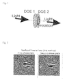
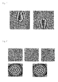
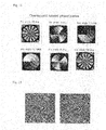
- FIG. 2 the phase pattern of two DOEs that act after combination as a Fresnel lens with a refractive power that depends on their mutual rotation angle.
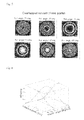
- FIG. 6 a plot of the diffraction efficiency and the refractive power of a Fresnel lens with avoided sectioning, as a function of the mutual rotation angle between the two DOEs.
- FIG. 7 the phase pattern of two DOEs that produce a combined DOE acting as a varifocal Fresnel lens with an offset of its refractive power.
- FIG. 8 the phase pattern of two DOEs that act after combination as an axicon with a refractive power that depends on the mutual rotation angle.
- FIG. 14 the resulting phase pattern of a superposition of the two DOEs of FIG. 13 at different mutual rotation angles.
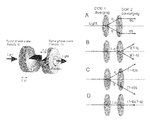
- FIG. 1 shows the principle setup of an optical device according to the present invention.
- Two DOEs are placed at a small mutual distance behind each other. They can be mutually rotated around a central axis that is perpendicular to their surfaces.
- the DOE combination manipulates the wavefront of an incident light wave in a predesigned way, that depends on the mutual rotation angle.
- the combination of two DOEs can yield a transmission function for various specific purposes, that can furthermore be continuously changed if the two DOEs are mutually rotated.
- the underlying principle is to some extent related to the Moiré effect, which is discussed, e.g., in S. Bara, Z. Jaroszewicz, A. Kolodziejczyk, and V. Moreno, “Determination of basic grids for subtractive moire patterns,” Appl. Opt. 30, 1258-1262 (1991), J. M. Burch and D. C. Williams, “Varifocal moiré zone plates for straightness measurement,” Appl. Opt. 16, 2445-2450 (1977), or Z. Jaroszewicz, A. Kolodziejczyk, A.
- the corresponding phase transmission function of the combined DOE system corresponds to that of the kinoform of an ideal lens that has—due to its asymmetric, sawtooth-like phase grating structure (due to the modulo 2 ⁇ operation) an unlimited diffraction efficiency, i.e. such a DOE element can be used for the designed light wavelength exactly like a “normal” glass lens without generating any undesired light contributions.
- the two DOEs have still the property that they have a mirror symmetry, i.e. they are identical phase structures if one of them is flipped upside down and placed “face-to-face” on top of the other one.
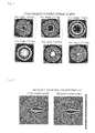
- phase values of the combined DOE system are again plotted in FIG. 5 for some positive and negative rotation angles ⁇ , namely ⁇ 75, ⁇ 30, ⁇ 15 degrees in the upper row and +15, +30, +70 degrees in the lower row.
- the graph in FIG. 6 thus shows, that a mutual rotation of the two DOEs by an angle between ⁇ 90 degrees and +90 degrees is possible, with only a low loss of 15% in the efficiency of the combined Fresnel lens.
- the corresponding Fresnel lens is periodically scanning in an adjustable range of focal lengths.
- This may have applications in imaging systems (inspection cameras) and beam scanning systems (bar-code readers etc.).
- a periodically rotating DOE lens which is combined with an imaging system that uses a shutter that is phase locked to the DOE rotation (i.e. the shutter opens always at a certain angular position of the DOE) sharply focuses at objects in a certain distance that depends on the relative phase between the shutter openings and the DOE rotation.
- the shutter acts electronically (e.g. a gateable image intensifier) focusing can be controlled purely by electronical means, by just varying the phase between DOE rotation and shutter openings.
- a max for a certain DOE depends on both, its pixel resolution and its maximal desired radius.
- the combined DOE then changes its focal length as a function of the mutual rotation angle as before, particularly with equal efficiency and equal change of refractive power as a function of the mutual rotation angle, however it has now an offset focal length corresponding to f offs .
- the two elements are still mirror images of each other (at a certain relative rotation) and thus it is sufficient to produce two identical elements with transmission function T lens1 , that are arranged face-to-face.
- An example of two DOEs that form after combination a varifocal Fresnel lens with an offset refractive power is shown in FIG. 7 .
- FIG. 8(E) An example is plotted in FIG. 8(E) , again for a mutual rotation angle of 25 degrees. Similar to the last section, there appears a second axicon structure that is superposed to the first one and that has a different refractive power. However, the relative efficiency of the second axicon structure is again below 15% as long as the mutual rotation angle is limited to the intervall between ⁇ 90 and +90 degrees.
- an “axicon lens” i.e. an axicon with a variable refractive power that is superposed by a “normal” focussing or diverging Fresnel lens of a fixed focal power f ⁇ 1 offs .
- Two successive, specially designed DOEs can act as a precise, continuously adjustable phase shifter when they are mutually rotated.
- phase shifting capability is required for example in optical interferometry, interference microscopy, holography, as well as in many scientific applications (like continuous phase shifting of standing light waves in atom trapping etc.).
- the DOE system can also act as a continuous frequency shifter of a transmitted light beam, if one of the DOEs is continuously rotated with respect to the other.
- Such a frequency shifter is required in interferometric (“heterodyning interferometry”) and scientific applications.
- helical index sometimes also denoted as “helical charge”
- the combined transmission function corresponds to a static, plane phase shift of m ⁇ that is imprinted on an incoming wave that passes the combined DOE element.
- the sign of the frequency (or phase) shift can be chosen by the rotational direction.
- Eq. (17) and Eq. (18) also show that the helical index m acts as an intrinsic “gear-transmission” factor, i.e. the phase- or frequency shift of a transmitted beam corresponds to the factor m that is multiplied by the rotation angle or by the rotation frequency of the rotating DOE, respectively.
- the main undesired contribution of wrongly manipulated light at each of the two DOEs will be the so-called zero diffraction order, i.e. a fraction of light that is just transmitted through the DOE without being influenced. Even if this zero order contribution is small, it can have a considerable effect at the total transmitted wave, since it coherently interferes with the remaining light, which will usually result in a spatial intensity modulation of the transmitted light wave that changes when the DOEs are mutually rotated.
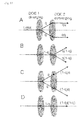
- FIG. 11 is not to scale, since the actual distance between the two DOEs is as close as possible, such that there is no actual beam expansion.
- the Figure shows a set of two DOEs, where the first one has a superposed diverging lens term (in addition to its tailored phase profile), whereas the second one has a superposed converging lens term of the same absolute refractive power.
- Part (A) of the figure shows the ideal case, where the light wave is diffracted to the desired first diffraction order by both of the DOEs.
- the outcoming wave has the same divergence as the incoming wave, and it has additionally the desired imprinted phasefront modulation.
- the total diffraction efficiency is q 2 .
- f div is the focal length of the superposed converging and diverging Fresnel lenses, and is preferably chosen as small as practically possible (limited by Eq. (11)) in order to achieve a fast “dilution” of the undesired beam components by divergence behind the DOE pair.
- a phase/frequency shifter produced by the DOE pair in the lower row has a significantly increased relative efficiency between the desired phase-shifted wave component, and residual non-diffracted components.
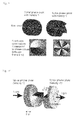
- Spiral phase elements have important applications in beam shaping for generating so-called doughnut beams, which are used for optical trapping (laser tweezers and atom traps), for transferring angular momentum to microscopic particles (optical pumps), and more recently for spiral phase contrast imaging in microscopy and interferometry.
- a set of two successive DOEs, that can act as a spiral phase element with a helical charge that can be continuously adjusted (and even inverted) in a selected range by adjusting the mutual rotation angle of the two DOEs is designed.
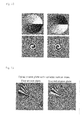
- FIG. 13 An example for a set of DOEs with the transmission functions according to Eq. (24) is shown in FIG. 13 .
- the resolution requirements are most stringent in the region around the center of the DOEs.
- the resulting combined transmission function after an overlapping of the two DOEs are shown in FIG. 14 for a number of mutual rotation angles, namely ⁇ 25, ⁇ 5, ⁇ 1.5, +1.5, +5, and +25 degrees.
- the corresponding transmission functions correspond to spiral phase elements with helical indices of approximately ⁇ 13, ⁇ 3, ⁇ 1, +1, +3, and +13, respectively.
- FIG. 15 An example for two DOEs that are calculated according to these transmission functions is shown in FIG. 15 .
- the transmission function of the combined DOE corresponds exactly to that of the previous pair of DOEs (see FIG. 13 ), but there is an increase in signal-to-noise ratio if the diffraction efficiency of the individual DOEs is smaller than 1, that is given by Eq. (21).
- Spiral phase elements for generating doughnut beams, or for spatial filtering purposes are usually produced as holograms, or as DOEs.
- the corresponding helical charge is not variable.
- Spiral phase elements with variable helical charge can be programmed at standard liquid crystal displays with a high resolution, or at customized liquid crystal displays. Both methods are very cost expensive. Also, the generation of a variable spiral phase element by controlled deformation of a special plexiglass disc with mechanical methods has been reported. However, this method requires very sophisticated mechanics and production methods.
- phase shifting is not continuous, i.e. the used optical elements have a “stopping position” from where they have to be reset to their respective “starting positions”, before the phase shifting can go on. This also prevents to use these methods as adjustable frequency shifters as can be done by a continuous mutual rotation of the DOEs according to the present invention.
- a known method to achieve a continuous phase shift is the use of the so-called Pancharatnam phase by a mutual rotation of a combination of two quarterwave and one halfwave plate in a beam path.
- the Pancharatnam method is only realizable for light in a certain polarization state.
- a particular advantage of the present invention is its high phase shifting accuracy, and the possibility to realize a “gear transmission”, i.e. to generate pairs of DOEs that produce a +/ ⁇ n f frequency shift (where n is an integer number which depends on the design of the DOEs and can reach 1000) when spatially rotated with f Hz.
Landscapes
- Physics & Mathematics (AREA)
- General Physics & Mathematics (AREA)
- Optics & Photonics (AREA)
- Diffracting Gratings Or Hologram Optical Elements (AREA)
- Mechanical Light Control Or Optical Switches (AREA)
Abstract
Description
T combi(x,y)=T 1(x,y)T 2(x,y), Eq. (1)
i.e. the phase landscape of the combined DOE is
Φcombi(x,y)=Φ1(x,y)+Φ2(x,y). Eq. (2)
T lens1(x,y)=exp[iar(x,y)2θ(x,y)] and T lens2(x,y)=exp[−iar(x,y)2θ(x,y)]. Eq. (3)
There x and y are the cartesian coordinates of a point (x,y) with the origin x=0, y=0 corresponding to the center of the plate, and r(x,y)=(x2+y2)1/2 and θ(x,y)=angle(x+iy) are the corresponding polar coordinates of the same point. As will be shown below, the constant a is proportional to the optical power of the combined DOE system. In order to create two DOEs from these transmission functions, only the phase of them has to be calculated at each point, and the result has to be taken modulo (2π) such that the result consists of an array of phase values in a range between 0 and 2π. The corresponding phase patterns of the two DOEs are plotted in 0.
T combi=exp(iar 2θ)exp(−iar 2(θ−φ)=exp(iaφr 2). Eq. (4)
f −1 =aφλ/π
(in diopters, corresponding to the inverse of the focal length f), where λ is the light wavelength. Therefore, the change of the optical power depends linearly on the mutual rotation angle between the two DOEs, i.e. df−1/dφ=aλ/π.
T lens1=exp[iround{ar 2}θ] and T lens2=exp[−iround{ar 2}θ] Eq.(6)
where the round{ . . . }-operation means rounding of the argument to the next higher integer number.
where p is the minimal size of one DOE pixel that is typically limited by the refraction process. The first and second conditions hold for the radial and tangential phase resolution, respectively. For DOEs generating Fresnel lenses it turns out that the first condition is always more restrictive than the second one, thus in the following it can be considered alone.
2armaxθmax<p−1, Eq. (8)
where rmax is the maximal radius of the DOE, and θmax is the maximal polar angle. Since θ is limited to a range between −π and π, θmax corresponds to π, and the condition becomes:
a<(2pr max)−1, i.e. a max(2pr max)−1. Eq. (9)
−f min −1 <f −1 <+f min −1, Eq. (10)
where
f min=4pr max/λ. Eq. (11)
is the smallest achievable focal length of the combined DOE system that is achieved at a mutual rotational angle of ±90 degrees, and that yields a diffraction efficiency of >85%.
T lens1=exp[iround{ar 2}θ]exp(iπr 2/2λf offs) and
T lens2=exp[iround{ar 2}θ]exp(iπr 2/2λf offs). Eq (12)
T axi1(x,y)=exp[iar(x,y)θ(x,y)] and T axi2(x,y)=exp[−iar(x,y)θ(x,y)]. Eq. (13)
T axi1=exp[iround{ar}θ] and T axi2=exp[−iround{ar}θ], Eq. (14)
T axi1=exp[i round{ar}θ]exp(inr 2/2λf offs) and
T axi2=exp[i round{ar}θ]exp(inr 2/2λf offs, Eq.(15)
and an example for a corresponding DOE is plotted in Error! Reference source not found.(C).
T phas1=exp(imθ) and T phas2=exp(−imθ), Eq. (16)
where the so-called helical index (sometimes also denoted as “helical charge”) m is an integer number. An example for such spiral phase plates is plotted in
T combi=exp(−imθ)exp(im(θ−φ))=exp(−imφ) Eq. (17)
Thus, the combined transmission function corresponds to a static, plane phase shift of mφ that is imprinted on an incoming wave that passes the combined DOE element.
ωout=ωin −mω rot Eq. (18)
S normal =I mod /I noise =q 2/(1−q 2) Eq. (19)
S optimal =q 2/(1−q)2. Eq. (20)
Thus the increase in signal-to-noise ratio between the optimized and the normal (Eq. (19)) DOE pair is:
S optimal /S normal=(1−q 2)/(1−q)2. Eq. (21)
T phas1=exp(imθ)exp(iπr 2 /λf div) and T phas2=exp(−imθ)exp(−iπr 2 /λf div). Eq. (22)
T spir1=exp(iaθ 2) and T spir2=exp(−iaθ 2), Eq. (23)
where a is a constant that determines the change in the helical index of the combined DOE as a function of the rotation angle. Thus the transmission function of the combined DOE at a mutual rotation angle of φ becomes:
T combi=exp(iaθ 2)exp(−ia[θ−φ] 2)=exp(2iaφθ)exp(−iaφ 2). Eq. (24)
T spir1=exp(iaθ 2)exp(iπr 2 /λf div) and T spir2=exp(−iaθ 2)exp(−iπr 2 /λf div), Eq. (25)
Claims (13)
T combi=T 1(r,θ)*T 2(r,θ−φ)=exp[iΦ 1(r,θ)]*exp[iΦ 2(r,θ−φ)]==exp[i{Φ1(r,θ)+Φ 2(r,θ−φ)}] where φ is the relative angle of rotation,
Φ1(r,θ)=mod2π{[F(r)θ+m phasθ+a spirθ2]+[G offs(r)/2]+a divr2} and
Φ2(r,θ)=mod2π{−[F(r)θ+m phasθ+a spirθ2]+[G offs(r)/2]−a divr2},
Φ1(r,θ)=mod2π{[a lens r 2θ+a axic rθ+m phasθ+a spirθ2]+(a offs/2)r 2+a div r 2} and
φ2(r,θ)=mod2π{[a lens r 2θ+a axic rθ+m phasθ+a spirθ2]+(a offs/2)r 2−a div r 2},
T combi=T 1(r,θ)*T 2(r,θ−φ)=exp[iΦ 1(r,θ)]*exp[iΦ 2(r,θ−φ)]==exp[i{Φ 1(r,θ)+Φ2(r,θ−φ)}] where φ is the relative angle of rotation,
φ1(r,θ)=mod2π{[round{F(r)}θ+m phasθ]+[G offs(r)/2]+a div r 2} and
φ2(r,θ)=mod2π{−[round{F(r)}θ+m phasθ]+[G offs(r)/2]−a div r 2},
φ1(r,θ)=mod2π{[round{a lens r 2 +a axic r}θ+m phasθ]+(a offs/2)r 2 +a div r 2} and
φ2(r,θ)=mod2π{−[round{a lens r 2 +a axic r}θ+m phasθ]+(a offs/2)r 2 −a div r 2},
Applications Claiming Priority (1)
| Application Number | Priority Date | Filing Date | Title |
|---|---|---|---|
| PCT/EP2007/006490 WO2009012789A1 (en) | 2007-07-20 | 2007-07-20 | Optical device with a pair of diffractive optical elements |
Publications (2)
| Publication Number | Publication Date |
|---|---|
| US20100134869A1 US20100134869A1 (en) | 2010-06-03 |
| US8335034B2 true US8335034B2 (en) | 2012-12-18 |
Family
ID=38578615
Family Applications (1)
| Application Number | Title | Priority Date | Filing Date |
|---|---|---|---|
| US12/452,711 Active 2028-01-19 US8335034B2 (en) | 2007-07-20 | 2007-07-20 | Optical device with a pair of diffractive optical elements |
Country Status (4)
| Country | Link |
|---|---|
| US (1) | US8335034B2 (en) |
| EP (1) | EP2174168B8 (en) |
| JP (1) | JP5622571B2 (en) |
| WO (1) | WO2009012789A1 (en) |
Cited By (4)
| Publication number | Priority date | Publication date | Assignee | Title |
|---|---|---|---|---|
| US9690882B2 (en) | 2011-09-29 | 2017-06-27 | Carl Zeiss Ag | Lens having an extended range of focus and method of making the same |
| US10261294B2 (en) | 2016-10-04 | 2019-04-16 | Samsung Electronics Co., Ltd. | Rotational varifocal planar lens |
| DE102018126381A1 (en) | 2018-02-15 | 2019-08-22 | Schott Ag | Method and device for inserting a dividing line into a transparent brittle material, as well as according to the method producible, provided with a dividing line element |
| US10393929B1 (en) | 2017-11-30 | 2019-08-27 | Facebook Technologies, Llc | Systems and methods for a projector system with multiple diffractive optical elements |
Families Citing this family (57)
| Publication number | Priority date | Publication date | Assignee | Title |
|---|---|---|---|---|
| DE202008017962U1 (en) * | 2008-09-23 | 2011-02-10 | Sick Ag | Illumination unit for generating a self-similar pattern |
| JP2010151948A (en) * | 2008-12-24 | 2010-07-08 | Hamamatsu Photonics Kk | Device and method for controlling light |
| JP2013509234A (en) | 2009-10-30 | 2013-03-14 | アッコレンズ インターナショナル ビー.ヴイ. | Variable focus intraocular lens |
| WO2011102719A1 (en) * | 2010-02-17 | 2011-08-25 | Akkolens International B.V. | Adjustable chiral ophthalmic lens |
| CN101881858B (en) * | 2010-06-11 | 2012-07-11 | 哈尔滨工程大学 | Satellite-type helical multi-core fiber optical micro-tweezers capable of achieving rotation of small particles and preparation method thereof |
| DE102011013613A1 (en) * | 2010-10-01 | 2012-04-05 | Carl Zeiss Microimaging Gmbh | Microscope and microscopy method |
| CN102122079A (en) * | 2011-03-23 | 2011-07-13 | 浙江大学 | Method and device for generating inhibition facula in stimulated emission depletion microscope |
| CN102226855B (en) * | 2011-05-26 | 2012-11-14 | 浙江大学 | Three-dimensional super-resolution focusing method and device based on transparent medium pellet |
| CN102213840B (en) * | 2011-05-26 | 2012-11-14 | 浙江大学 | Method and device for producing dark spot on basis of transparent medium small ball |
| GB201110954D0 (en) * | 2011-06-28 | 2011-08-10 | The Technology Partnership Plc | Optical device |
| WO2013033591A1 (en) * | 2011-08-31 | 2013-03-07 | President And Fellows Of Harvard College | Amplitude, phase and polarization plate for photonics |
| US9864114B2 (en) * | 2011-09-28 | 2018-01-09 | Hitachi, Ltd. | Zone plate having annular or spiral shape and Y-shaped branching edge dislocation |
| DE102011055777B4 (en) * | 2011-11-28 | 2015-02-26 | Carl Zeiss Ag | Optical device, optical element and method of making the same |
| DE102012103008B3 (en) * | 2012-04-05 | 2013-10-10 | Fraunhofer-Gesellschaft zur Förderung der angewandten Forschung e.V. | Method and device for distance measurement with a diffractive structure |
| US9671566B2 (en) * | 2012-06-11 | 2017-06-06 | Magic Leap, Inc. | Planar waveguide apparatus with diffraction element(s) and system employing same |
| PL400340A1 (en) | 2012-08-12 | 2014-02-17 | Instytut Optyki Stosowanej | System for measuring the lateral displacement of objects and determination of the geodetic reference line |
| EP2705812A1 (en) * | 2012-09-05 | 2014-03-12 | Universität zu Lübeck | Device for laser cutting within transparent materials |
| EP2982949B1 (en) * | 2012-10-05 | 2020-04-15 | National University Corporation Kagawa University | Spectroscopic measurement device |
| KR20140062346A (en) * | 2012-11-14 | 2014-05-23 | 한국전자통신연구원 | Apparatus for generating proton beam and treatment method using the same |
| JP6516134B2 (en) * | 2013-06-29 | 2019-05-22 | 堀 健治 | Filter, lens, imaging optical system and imaging system having phase conversion function |
| US10228242B2 (en) | 2013-07-12 | 2019-03-12 | Magic Leap, Inc. | Method and system for determining user input based on gesture |
| WO2015006784A2 (en) | 2013-07-12 | 2015-01-15 | Magic Leap, Inc. | Planar waveguide apparatus with diffraction element(s) and system employing same |
| WO2015057720A1 (en) * | 2013-10-14 | 2015-04-23 | Huawei Technologies Co., Ltd. | System and method for optical fiber |
| JP6057954B2 (en) * | 2014-01-10 | 2017-01-11 | 新和工業株式会社 | Lens, sensor device and lighting device |
| WO2015118540A1 (en) | 2014-02-06 | 2015-08-13 | Bar Ilan University | System and method for imaging with pinhole arrays |
| US9500586B2 (en) * | 2014-07-24 | 2016-11-22 | Nxgen Partners Ip, Llc | System and method using OAM spectroscopy leveraging fractional orbital angular momentum as signature to detect materials |
| EP3026479A1 (en) | 2014-11-28 | 2016-06-01 | Sick Ag | Camera system |
| DE202014105767U1 (en) | 2014-11-28 | 2016-03-01 | Sick Ag | camera system |
| DE102015105613B4 (en) * | 2015-04-13 | 2023-08-31 | Carl Zeiss Industrielle Messtechnik Gmbh | Reflected light illumination for a variable working distance |
| US9645417B2 (en) * | 2015-04-14 | 2017-05-09 | Honeywell International Inc. | Preparation cell systems and methods of a preparing a state of laser light |
| US9618664B2 (en) * | 2015-04-15 | 2017-04-11 | Finisar Corporation | Partially etched phase-transforming optical element |
| DE102016125255A1 (en) * | 2016-12-21 | 2018-06-21 | Carl Zeiss Jena Gmbh | Wavefront manipulator and optical device |
| WO2018136806A1 (en) * | 2017-01-20 | 2018-07-26 | President And Fellows Of Harvard College | Optical devices including rotary variable optical elements |
| CN106918903A (en) * | 2017-03-29 | 2017-07-04 | 西安交通大学 | A kind of optics rotates Doppler frequency converter |
| DE112018002670T5 (en) | 2017-05-24 | 2020-03-05 | The Trustees Of Columbia University In The City Of New York | Broadband achromatic flat optical components due to dispersion-technical dielectric meta-surfaces |
| WO2019046827A1 (en) | 2017-08-31 | 2019-03-07 | Metalenz, Inc. | Transmissive metasurface lens integration |
| CN109469881A (en) * | 2017-09-08 | 2019-03-15 | 法雷奥照明公司 | Photo-patterning device, car light and motor vehicles including the photo-patterning device |
| DE102018201998B4 (en) | 2018-02-08 | 2021-03-04 | Minebea Mitsumi Inc. | Optical device and zoom lens with at least two lenses that can be rotated relative to one another |
| JP7191311B2 (en) * | 2018-03-05 | 2022-12-19 | 国立大学法人徳島大学 | A spectrometer using a spectroscopic element with a light-collecting function |
| CN109814184A (en) * | 2019-03-20 | 2019-05-28 | 中国工程物理研究院激光聚变研究中心 | The production method of complex optics lens, laser aid and Diode laser vortex beams |
| US11978752B2 (en) | 2019-07-26 | 2024-05-07 | Metalenz, Inc. | Aperture-metasurface and hybrid refractive-metasurface imaging systems |
| KR102539943B1 (en) * | 2019-09-10 | 2023-06-08 | 한국기초과학지원연구원 | Reflective spiral phase plate and laguerre gaussian beam generating appartus comprising the same |
| RU2728214C1 (en) * | 2019-11-01 | 2020-07-28 | федеральное государственное автономное образовательное учреждение высшего образования "Национальный исследовательский университет ИТМО" (Университет ИТМО) | Method of manufacturing multisector spiral phase plate with variable phase delay (svr) |
| CN111308724A (en) * | 2019-11-26 | 2020-06-19 | 中国科学院光电技术研究所 | Long-focus light-generating nanometer light pipe generation method based on radial polarized light |
| WO2021156148A1 (en) | 2020-02-07 | 2021-08-12 | Medizinische Universität Innsbruck | Modified moiré lens |
| JP7468861B2 (en) | 2020-03-31 | 2024-04-16 | 三菱重工業株式会社 | Phase difference measurement device, beam output device, and phase difference measurement method |
| US11762220B2 (en) * | 2020-04-30 | 2023-09-19 | Coopervision International Limited | Multifocal ophthalmic lenses and related methods |
| US11934043B2 (en) | 2020-04-30 | 2024-03-19 | Coopervision International Limited | Myopia control lens and related methods |
| US11754858B2 (en) * | 2020-04-30 | 2023-09-12 | Coopervision International Limited | Multifocal ophthalmic lens and related methods |
| CN112034627B (en) * | 2020-08-11 | 2023-06-23 | 北京润和微光科技有限公司 | DOE-based focusing circular ring light spot generation method and system |
| CN112505914B (en) * | 2020-12-10 | 2022-03-22 | 武汉先河激光技术有限公司 | Vortex light beam generation system and method and phase modulation combination device |
| CN112540457B (en) * | 2020-12-10 | 2021-10-15 | 武汉先河激光技术有限公司 | Vortex light beam generation device, system and method with adjustable topological number |
| CN113900265A (en) * | 2021-10-26 | 2022-01-07 | 北京润和微光科技有限公司 | Variable wedge angle axicon system based on cascade diffraction optical element |
| CN113977072B (en) * | 2021-11-30 | 2022-10-18 | 广东宏石激光技术股份有限公司 | Variable-spot diffraction element-based zoom laser processing system and method |
| US11927769B2 (en) | 2022-03-31 | 2024-03-12 | Metalenz, Inc. | Polarization sorting metasurface microlens array device |
| WO2024029309A1 (en) * | 2022-08-02 | 2024-02-08 | 富士フイルム株式会社 | Lens device |
| CN116560163A (en) * | 2023-04-24 | 2023-08-08 | 信扬科技(佛山)有限公司 | Imaging device and electronic device |
Citations (7)
| Publication number | Priority date | Publication date | Assignee | Title |
|---|---|---|---|---|
| US5680253A (en) | 1991-03-27 | 1997-10-21 | Fujitsu Limited | Light beam scanning apparatus comprising a first and second diffraction grating plate |
| US5880846A (en) * | 1997-07-09 | 1999-03-09 | Yeda Research And Development Co. Ltd. | Method and apparatus for color-coded optical profilometer |
| US6154278A (en) * | 1993-06-10 | 2000-11-28 | Matsushita Electric Industrial Co., Ltd. | Optical encoder for optically measuring displacement of moving body |
| US6442312B1 (en) * | 1997-07-08 | 2002-08-27 | Oki Electric Industry Co., Ltd. | Optical filter fabrication method and apparatus, optical filter, fiber holder with spiral groove, and phase mask |
| US20030179804A1 (en) | 2002-03-22 | 2003-09-25 | Cook Lacy G. | Method and laser beam directing system with rotatable diffraction gratings |
| US20060028961A1 (en) | 2004-08-05 | 2006-02-09 | Sung-Ha Kim | Illumination system capable of eliminating laser speckle and projection system employing the same |
| US7671986B2 (en) * | 2007-07-30 | 2010-03-02 | Bwt Property, Inc | Spectroscopy apparatus based on hetero-junction phototransistors |
-
2007
- 2007-07-20 WO PCT/EP2007/006490 patent/WO2009012789A1/en active Application Filing
- 2007-07-20 US US12/452,711 patent/US8335034B2/en active Active
- 2007-07-20 JP JP2010517272A patent/JP5622571B2/en not_active Expired - Fee Related
- 2007-07-20 EP EP07786238.1A patent/EP2174168B8/en not_active Not-in-force
Patent Citations (7)
| Publication number | Priority date | Publication date | Assignee | Title |
|---|---|---|---|---|
| US5680253A (en) | 1991-03-27 | 1997-10-21 | Fujitsu Limited | Light beam scanning apparatus comprising a first and second diffraction grating plate |
| US6154278A (en) * | 1993-06-10 | 2000-11-28 | Matsushita Electric Industrial Co., Ltd. | Optical encoder for optically measuring displacement of moving body |
| US6442312B1 (en) * | 1997-07-08 | 2002-08-27 | Oki Electric Industry Co., Ltd. | Optical filter fabrication method and apparatus, optical filter, fiber holder with spiral groove, and phase mask |
| US5880846A (en) * | 1997-07-09 | 1999-03-09 | Yeda Research And Development Co. Ltd. | Method and apparatus for color-coded optical profilometer |
| US20030179804A1 (en) | 2002-03-22 | 2003-09-25 | Cook Lacy G. | Method and laser beam directing system with rotatable diffraction gratings |
| US20060028961A1 (en) | 2004-08-05 | 2006-02-09 | Sung-Ha Kim | Illumination system capable of eliminating laser speckle and projection system employing the same |
| US7671986B2 (en) * | 2007-07-30 | 2010-03-02 | Bwt Property, Inc | Spectroscopy apparatus based on hetero-junction phototransistors |
Non-Patent Citations (5)
| Title |
|---|
| Bara et al., Determination of Basic Grids for Substractive Moire patterns, Applied Optics, vol. 30, No. 10, pp. 1258-1262, Apr. 1, 1991. |
| Jaroszewicz et al., Equilateral Hyperbolic Moire Zone Plates with Variable Focus Obtained by Rotations, Optic Express 918, vol. 13, No. 3, 8 pages, Feb. 7, 2005. |
| Kolodziejcyk et al, Diffractive Elements of Variable Optical Power and High Diffraction Efficiency, Applied optics, OSA, Optical Society of America, Wshington, D.C, US, vol. 32, No. 23, pp. 4317-4322, Aug. 10, 1993. |
| Lohmann, A New Class of Varifocal Lens, Applied Optics, vol. 9, No. 7, pp. 1669-1691, Jul. 1970. |
| ZzzzzBurch et al., Varifocal Moire Zone Plates for Straightness Measurement, Applied Optics, vol. 16, No. 9, pp. 2445-2450, Sep. 1977. |
Cited By (7)
| Publication number | Priority date | Publication date | Assignee | Title |
|---|---|---|---|---|
| US9690882B2 (en) | 2011-09-29 | 2017-06-27 | Carl Zeiss Ag | Lens having an extended range of focus and method of making the same |
| US10261294B2 (en) | 2016-10-04 | 2019-04-16 | Samsung Electronics Co., Ltd. | Rotational varifocal planar lens |
| US10725273B2 (en) | 2016-10-04 | 2020-07-28 | Samsung Electronics Co., Ltd. | Rotational varifocal planar lens |
| US11300777B2 (en) | 2016-10-04 | 2022-04-12 | Samsung Electronics Co., Ltd. | Rotational varifocal planar lens |
| US10393929B1 (en) | 2017-11-30 | 2019-08-27 | Facebook Technologies, Llc | Systems and methods for a projector system with multiple diffractive optical elements |
| DE102018126381A1 (en) | 2018-02-15 | 2019-08-22 | Schott Ag | Method and device for inserting a dividing line into a transparent brittle material, as well as according to the method producible, provided with a dividing line element |
| WO2019158488A1 (en) | 2018-02-15 | 2019-08-22 | Schott Ag | Method and device for inserting a separation line into a transparent, brittle-fracture material, and element that can be produced according to the method and is provided with a separation line |
Also Published As
| Publication number | Publication date |
|---|---|
| JP2010533895A (en) | 2010-10-28 |
| JP5622571B2 (en) | 2014-11-12 |
| EP2174168B8 (en) | 2017-12-06 |
| EP2174168B1 (en) | 2017-10-25 |
| WO2009012789A1 (en) | 2009-01-29 |
| EP2174168A1 (en) | 2010-04-14 |
| US20100134869A1 (en) | 2010-06-03 |
Similar Documents
| Publication | Publication Date | Title |
|---|---|---|
| US8335034B2 (en) | Optical device with a pair of diffractive optical elements | |
| US10802259B2 (en) | Structured illuminating apparatus, structured illuminating microscopy apparatus, and structured illuminating method | |
| US12092815B2 (en) | Methods and systems for generating virtual content display with a virtual or augmented reality apparatus | |
| Kamali et al. | A review of dielectric optical metasurfaces for wavefront control | |
| US7390618B2 (en) | Manufacturing method of microstructure, manufacturing method and manufacturing device of electronic device | |
| JP6250535B2 (en) | Method and apparatus for stacking thin volume grating stacks and beam combiner for holographic display | |
| US9477091B2 (en) | Multi-dimensional imaging using multi-focus microscopy | |
| Bernet et al. | Adjustable refractive power from diffractive moiré elements | |
| US20170219739A1 (en) | Spatially Multiplexed Dielectric Metasurface Optical Elements | |
| JP5907998B2 (en) | Variable orientation lighting pattern rotator | |
| US9535241B2 (en) | Structured illuminating microscopy and structured illuminating observation method | |
| US10054859B2 (en) | Real-time variable parameter micro-nano optical field modulation system and interference lithography system | |
| US10871601B2 (en) | Volume holographic optical elements for imaging with reduced aberrations | |
| JP2013502703A (en) | Polarization conversion unit, illumination optical system, exposure apparatus, and device manufacturing method | |
| Bernet | Combined diffractive optical elements with adjustable optical properties controlled by a relative rotation: tutorial | |
| RU2458367C2 (en) | Optical device with pair of diffraction optical elements | |
| US20240295702A1 (en) | Wave front manipulator with diffractive components | |
| Faraon et al. | Applications of wavefront control using nano-post based dielectric metasurfaces | |
| Brunner et al. | Advanced optical components | |
| US20240085602A1 (en) | System and method for fabricating polarization holograms | |
| Khonina et al. | Exploring Diffractive Optical Elements and Their Potential in Free Space Optics and imaging‐A Comprehensive Review | |
| Tai et al. | Design and fabrication of a wide-field holographic lens for a laser communication receiver | |
| Room | Joint Session with International Optical Design Conference | |
| Solano | Diffractive Optical Components |
Legal Events
| Date | Code | Title | Description |
|---|---|---|---|
| AS | Assignment |
Owner name: MEDIZINISCHE UNIVERSITAT INNSBRUCK,AUSTRIA Free format text: ASSIGNMENT OF ASSIGNORS INTEREST;ASSIGNORS:BERNET, STEFAN;RITSCH-MARTE, MONIKA;REEL/FRAME:023829/0869 Effective date: 20100113 Owner name: MEDIZINISCHE UNIVERSITAT INNSBRUCK, AUSTRIA Free format text: ASSIGNMENT OF ASSIGNORS INTEREST;ASSIGNORS:BERNET, STEFAN;RITSCH-MARTE, MONIKA;REEL/FRAME:023829/0869 Effective date: 20100113 |
|
| STCF | Information on status: patent grant |
Free format text: PATENTED CASE |
|
| REMI | Maintenance fee reminder mailed | ||
| FPAY | Fee payment |
Year of fee payment: 4 |
|
| SULP | Surcharge for late payment | ||
| MAFP | Maintenance fee payment |
Free format text: PAYMENT OF MAINTENANCE FEE, 8TH YEAR, LARGE ENTITY (ORIGINAL EVENT CODE: M1552); ENTITY STATUS OF PATENT OWNER: LARGE ENTITY Year of fee payment: 8 |
|
| FEPP | Fee payment procedure |
Free format text: MAINTENANCE FEE REMINDER MAILED (ORIGINAL EVENT CODE: REM.); ENTITY STATUS OF PATENT OWNER: LARGE ENTITY |